Embed Size (px)
Citation preview

CHARACTERIZATION OF ION IMPLANTED SURFACES BY LASER INDUCED BREAKDOWN
SPECTROSCOPY, LIBS
A Thesis Submitted to the Graduate School of Engineering and Science of
İzmir Institute of Technology in Partial Fulfillment of the Requirements for the Degree of
MASTER OF SCIENCE
in Chemistry
by Sabiha ÖRER
January 2008
İZMİR

We approve the thesis of Sabiha ÖRER
Assoc. Prof. Dr. Şerife YALÇIN Supervisor
Prof. Dr. Orhan ÖZTÜRK Committee Member
Asst. Prof.Dr. Ritchie EANES Committee Member
2 January 2008
Date Prof. Dr. Levent ARTOK Prof. Dr. Hasan BÖKE Head of Department of Chemistry Department Dean of the Graduate School of
Engineering and Science

ACKNOWLEDGMENT
I have been accompanied and supported by many people during this thesis study.
I have now the opportunity to express my gratitude to all of them. The first person I would like to thank is Assoc. Prof. Dr. Şerife YALÇIN who
not only guided me as my supervisor but also encouraged, and challenged me
throughout my master program. Her wide knowledge and her logical way of thinking
have been of great value to me.
My sincere thanks to Prof. Dr. Raşit TURAN for his generosity of letting us use
their Ge implanted samples.
Prof. Dr. Orhan ÖZTÜRK, Asst. Prof. Dr. Ritchie EANES, Prof. Dr. Serdar
ÖZÇELİK and Asst. Prof. Dr. Süleyman TARI deserve a special thanks as my thesis
committee members. I would like to thank all of them for their valuable comments and
suggestions.
Moreover, I am grateful to Asst. Prof. Dr. Çağlar KARAKAYA for sharing his
optical microscope and Assoc. Prof. Dr. Salih OKUR for AFM measurements.
My appreciation and thanks for the accomplishment of this study are directed to
group members of the Materials Research Center of İYTE for the SEM-EDX and AFM
analyses.
I am pleased to acknowledge TUBITAK for financial support (Project No.
105T134) .
I also feel deeply indebted to my research friend Resch. Assist. Arzu ERDEM
not only because of her friendship but also for her kind efforts and endless support.
I would like to thank all my friends at İYTE, especially Resch. Assist. Pınar
KASAPLA and Burcu ALTIN for their unfailing encouragement, neverending
friendship and support during my thesis.
Lastly, and most importantly, I wish to thank my family. I especially thank to
Evren MERT for making a difference in my life, to my parents Hikmet and Hüseyin
ÖRER and to my sister Gülümser ÖRER for their love and support all through my life.
With my deepest gratitude, I dedicate this study to my family.
iv
ABSTRACT
CHARACTERIZATION OF ION IMPLANTED SURFACES BY LASER INDUCED BREAKDOWN SPECTROSCOPY, LIBS
Laser Induced Breakdown Spectroscopy, LIBS, is a versatile atomic emission
spectrometric technique for the determination of the elemental composition of solids,
liquids, gases and aerosols with the need for little or no sample preparation.
In this study, an optical LIBS system from its conventional parts was designed,
constructed and optimized for spectrochemical analysis of solid materials. Specifically,
the 2-D elemental distribution of Ge ions on silicon oxide surfaces, prepared by the
method of ion implantation, with differing atomic concentrations between 1016 - 1017
ions/cm2 have been investigated by LIBS. For this purpose a Nd: YAG laser operating
at the second harmonic wavelength, 532 nm, was used to create a plasma on the
material surfaces. Spatially and temporally resolved atomic emission from the luminous
plasma was detected by an Echelle spectroctrograph and Intensified Charged Coupled
Device (ICCD) detector combination.
Spectral emission intensity from the LIBS measurements has been optimized
with respect to time, crater size, ablation depth and laser energy. Atomic Force
Microscopy (AFM) and Scanning Electron Microscopy (SEM) coupled with Energy
Dispersive X-Ray Spectroscopy (EDX) have been utilized to obtain crater depth,
morphology and elemental composition of the sample material, respectively. LIBS
spectral data revealed the possibility of performing 2-D distribution analysis of Ge ions
over the silicon oxide substrate at Ge ion concentrations lower than 0.5% (atomic).
LIBS as a fast semi-quantitative analysis method with 50µm lateral and 800 nm depth
resolutions has been evaluated. In this wok, elemental analysis of some metal surfaces,
such as Al and Cu, was also performed by LIBS.
Keywords: LIBS, surface analysis, Ge ion implantation, lateral resolution,
v
ÖZET
LAZER OLUŞTURMALI PLAZMA SPEKTROSKOPİSİ, LIPS, İLE İYON EKİLMİŞ YÜZEYLERİN KARAKTERİZASYONU
Lazer Oluşturmalı Plazma Spektroskopisi, LIBS, malzeme hazırlama işlemi en
az seviyede ya da hiç olmadan, katı, sıvı, gaz ve aerosollerin elemental
kompozisyonunu belirlemede son yıllarda yaygın olarak kullanılan bir atomik emisyon
spektrometresi tekniğidir.
Bu çalışmada, katı malzemelerin spektrokimyasal analizleri için bir Lazer
Oluşturmalı Plazma Spektrometresinin tasarım, kurulum ve optimizasyon çalışmaları
gerçekleştirilmiştir. Özellikle, 1016 - 1017 iyon/cm2 iyon konsantrasyonlarında iyon
ekleme metodu ile silikon oksit yözeyine ekilmiş germanyum iyonlarının 2-boyutlu
elemental dağılımı incelenmiştir. Bu amaçla, bir Nd: YAG lazerinin 532 nm’deki ikincil
harmonik ışıması kullanılmıştır. Oluşan ışıklı plazmanın atomik emisyonu, Eşel tipi bir
spektrograf ve şiddetlendirilmiş bir CCD detektör, ICCD, ile uzamsal ve zamansal
olarak incelenmiştir.
Laser Oluşturmalı Plazma ölçümlerinden elde edilen spektral emisyon şiddeti,
zaman, krater büyüklüğü, aşındırma derinliği ve lazer enerjisi bakımından optimize
edilmiştir. Oluşan kraterlerin derinliğini, morfolojisini ve elemental kompozisyonunu
belirlemede Atomik Kuvvet Mikroskobu (AFM) ve Enerji Dağılımlı X-Ray
spektroskopisi ile eşleştirilmiş Taramalı Elektron Mikroskobu (SEM), kullanılmıştır.
LIBS spektral verileri, silikon oksit üzerine ekilmiş Ge iyonlarının iki boyutlu (2-D)
elemental kompozisyon dağılımının % 0,5 (atomik) den daha az miktarlarda tayin
edilebileceğini göstermiştir. Kurulan LIBS sisteminin 50µm yüzeysel ve 800 nm
derinlik çözünürlüğünde hızlı bir yarı-kantitatif analiz metodu olarak kulanılabilirliği
değerlendirilimiştir. Ayrıca Al ve Cu gibi metal yüzeylerinin elemental analizleri de
yapılmıştır.
Anahtar kelimeler: LIPS, yüzey analizi, Ge iyonu ekimi, yanlamasına çözünürlük.
vi
TABLE OF CONTENTS
LIST OF FIGURES .......................................................................................................viii
LIST OF TABLES........................................................................................................... ix
CHAPTER 1. INTRODUCTION ..................................................................................... 1
1.1. Laser Induced Breakdown Spectroscopy, LIBS ................................ 1
1.2. Advantages and Disadvantages of Laser Induced ...............................
Breakdown Spectroscopy, LIBS......................................................... 2
1.3. Laser Induced Breakdown Spectroscopy Instrumentation ................ 3
1.3.1. Lasers ........................................................................................... 3
1.3.1.1. Solid-State Lasers ..................................................................... 5
1.3.1.2. Gas Lasers................................................................................. 5
1.3.1.3. Dye Lasers ................................................................................ 6
1.3.1.4. Semiconductor Diode Lasers .................................................... 6
1.3.2. Focusing and Collection Optics................................................... 6
1.3.3. Spectrograph & Detector ............................................................. 6
CHAPTER 2. SURFACE ANALYSIS BY LIBS ............................................................ 9
2.1. Surface Analysis ................................................................................ 9
2.1.1. Two Dimensional (2-D) Compositional Mapping....................... 9
2.1.2. Depth Profiling .......................................................................... 10
2.2. Aim of Study................................................................................... 12
2.3. Applied Methods.............................................................................. 12
2.3.1. Scanning Electron Microscopy (SEM) ...................................... 13
2.3.2. Atomic Force Microscope (AFM) ............................................. 14
CHAPTER 3. EXPERIMENTAL................................................................................... 15
3.1. Materials .......................................................................................... 15
3.1.1. Silicon ........................................................................................ 15
3.1.2. Germanium ................................................................................ 15
3.1.3. Ion Implantation......................................................................... 16
3.2. LIBS Experimental Set-up............................................................... 17
vii
3.3. SEM/EDX Analysis......................................................................... 19
3.4. AFM Analysis.................................................................................. 20
CHAPTER 4. RESULTS AND DISCUSSION.............................................................. 21
4.1. Spectral Analysis by LIBS............................................................... 21
4.2. Signal Optimization ......................................................................... 27
4.2.1. Focusing Lens to Sample Distance Adjustment ........................ 27
4.2.2. Time Resolution......................................................................... 28
4.2.3. Germanium Signal Intensity and Implantation Dose................. 30
4.2.4. Effect of Laser Energy............................................................... 31
4.2.5. Crater Size.................................................................................. 33
4.3. Two Dimensional (2-D) Compositional Mapping........................... 35
4.3.1. LIBS Analysis............................................................................ 35
4.3.2. SEM/EDX Analysis................................................................... 39
4.4. Depth Analysis................................................................................. 42
4.4.1. AFM Analysis............................................................................ 42
4.4.2. LIBS Spectral Analysis.............................................................. 44
CHAPTER 5. CONCLUSIONS ..................................................................................... 45
REFERENCES ............................................................................................................... 46

viii
LIST OF FIGURES Figure Page
Figure 1.1. A typical LIBS set up. .................................................................................... 3
Figure 1.2. A laser and its components............................................................................. 4
Figure 1.3. An echelle polychromator system. ................................................................. 7
Figure 1.4. ICCD detector................................................................................................. 8
Figure 3.1. Schematical representation of ion implantation process ............................. 16
Figure 3.2. Experimental setup for LIBS........................................................................ 18
Figure 4.1. Typical LIBS emission spectrum of an Al target. ....................................... 23
Figure 4.2. Typical LIBS emission spectrum of a Cu target .......................................... 24
Figure 4.3. Typical LIBS emission spectrum of a pure silicon wafer. ........................... 25
Figure 4.4. Typical LIBS emission spectrum of Ge implanted silicon wafer. ............... 26
Figure 4.5. Optical microscope images for focusing lens............................................... 27
Figure 4.6. Time resolved spectra of Ge implanted samples at several
gate delay times and laser pulses .................................................................. 29
Figure 4.7. Germanium growth curves for Ge (303.9 nm) line ...................................... 30
Figure 4.8. Relative signal intensities at different laser energies. .................................. 32
Figure 4.9. SEM images of the craters............................................................................ 34
Figure 4.10. Relationship of laser energy to crater size.................................................. 35
Figure 4.11. SEM image of the Ge-ion implanted Si wafer ........................................... 36
Figure 4.12. Ge ion distribution on implanted SiO2 surfaces. ....................................... 38
Figure 4.13. Contour plot showing the 2-D Ge ion distribution on
as SiO2 matrix. ........................................................................................... 39
Figure 4.14. SEM image of a 33.88 μm crater ............................................................... 40
Figure 4.15. SEM-EDX line scans analysis for Ge ion distribution............................... 42
Figure 4.16. Atomic force microscope image................................................................. 43
Figure 4.17. Relative intensities of Si-288.15 and Ge-303.91 nm lines ......................... 44

ix
LIST OF TABLES Table Page
Table 3.1. LIBS system specifications............................................................................ 19
Table 4.1. Spectral emission wavelengths of materials used.......................................... 21
Table 4.2. SEM-EDX measurements.............................................................................. 41

1
CHAPTER 1
INTRODUCTION
1.1. Laser Induced Breakdown Spectroscopy, LIBS
Lasers have been proposed and utilized as atomization sources in analytical
atomic spectroscopy, for decades. Laser Induced Breakdown Spectroscopy, LIBS, is a
spectrochemical analysis technique in which lasers are used for vaporization,
atomization and ionization steps. LIBS is also known as Laser Induced Plasma
Spectroscopy (LIPS) and Laser Ablation Spectroscopy (LAS).
In LIBS, a powerful laser pulse is brought to a sharp focus onto a target (solid,
liquid, or gas) by using a focusing lens. A thin layer of the material is spontaneously
ablated from the target surface, and then it subsequently gains energy from the laser
beam. The ablated material is suddenly heated by generating hot plasma with a
temperature of nearly 20,000 K and an electron density of 1016 – 1020 electrons/cm3
(Sneddon 1997). At these temperatures, the ablated material breaks down into excited
ionic and atomic species. The spectral emission of these species is collected by suitable
optical lenses and sent onto the entrance slit of a spectrograph and a detector. Spectral
analysis of the plasma can be used to determine the elemental composition, spatial
distribution and several other properties of ablated sample (Sneddon 1997).
LIBS has been used in a variety of applications including : the Mars exploration
(Brennetot 2003, Cremers 2000), cultural heritage studies (Anglos 2007), identification
of bioaerosols (Dixon, et al. 2005), trace element analysis of powdered samples (Gondal
2006), enviromental monitoring of heavy metals (Mirov 1999), identification of teeth
affected by caries (Samek 2001), and analysis of papers (Häkänken 2001).

2
1.2. Advantages and Disadvantages of Laser Induced Breakdown
Spectroscopy, LIBS
Laser Induced Breakdown Spectroscopy, LIBS has been evaluated as an
alternative method to other conventional plasma atomic emission spectrometric
techniques, such as, Inductively Coupled Plasma Atomic Emission Spectrometry, (ICP-
AES), and Direct Current Plasma Atomic Emission Spectrometry, (DCP-AES),
Microwave Induced Plasma (MIP-AES), Arc-AES, Spark-AES, Glow Discharge-OES
or even Glow Discharge-Mass Spectrometry (Winefordner 2004).
Several significant advantages make LIBS more applicable than others as
follows:
i) Little or no sample preparation makes it quick and easily adaptable to
chemical monitoring equipments or portable units;
ii) LIBS is capable of determining elemental compositions of various
materials regardless of whether the sample is solid, liquid, gas or aerosol;
iii) Since it is an emission technique, direct analysis of plasma provides
simultaneous multi-elemental analysis;
iv) The technique can be used to analyze extremely hard materials that are
difficult to digest and dissolve;
v) The spatial and temporal resolution is high since plasma light is
extremely bright, so that all atomic species are accessible; and
vi) There is also the option of using LIBS for remote analyses.
(Winefordner 2004).
However, difficulty in obtaining suitable standards is a disadvantage for LIBS.
Thus, LIBS can be considered a semiquantitative analysis technique. LIBS has poor
precision typically ranging between 5-10 % mainly due to the fluctuations in laser
energy and shot-to-shot reproducibility (Winefordner 2004).

3
1.3. Laser Induced Breakdown Spectroscopy Instrumentation A typical LIBS system consists of a pulsed laser, a focusing lens, collection
lenses and a spectrometer with a wide spectral range and a high sensitivity, fast
response rate, time-gated detector (Figure 1.1).
Figure 1.1. A typical LIBS set up
(Source: Radziemski 1989)
In this section each part of the typical LIBS system components will be
explained in detail.
1.3.1. Lasers The word LASER is an acronym for Light Amplification by Stimulated
Emission of Radiation. A laser is a quantum-mechanical device that creates and
amplifies a narrow, intense beam of coherent light. A laser consists of an active lasing
medium, a high reflective mirror and a partially transmissive mirror (output coupler)
(Figure 1.2).
Focusing Lens
Target
Laser
Plasma Collimating Lenses
Spectrograph & Detector
Data Acqusition and Control

4
Figure 1.2. A laser and its components
(Source: Skoog, et al. 1997)
The active lasing medium is the heart of the laser and may be in the form of gas,
liquid, solid or free electrons. This lasing medium is energized or pumped by an
external energy source (electricity or flash lamps) and absorbs this energy.
Consequently, electrons in the active medium are excited to higher energy levels.
Population inversion is successful if the number of particles in one excited state exceeds
the number of particles in some lower-energy state. Thus, stimulated emission is
observed and light is amplified (Skoog, et al. 1997).
An optical cavity consists of a pair of mirrors arranged such that light is
reflected back and forth by passing through the active medium. Throughout each
passage, the intensity of light is amplified by generation of additional photons. One of
the mirrors in the optical cavity is partially transparent and is called the output coupler.
The output laser beam is emitted through this mirror (Skoog, et al. 1997). Lasers are generally classified according to laser material and pump material.
Silfvast et al. (1996) notes that the major types of lasers are as follows:
• Solid state lasers
• Gas lasers
• Dye lasers
• Semiconductor diode lasers.

5
1.3.1.1. Solid-State Lasers
Solid-state lasers (Siegman 1986) use solids as an active lasing medium and
are optically pumped with discharge lamps or laser diodes. Generally, the active
medium of these types of lasers consist of a crystal or glass doped with a small amount
of rare earth elements or transition metal ions such as neodymium, chromium or erbium
(Sneddon 1997). In solid-state lasers, a high or low output power (a few milliwatts or
many kilowatts) with a high beam quality and ultra short pulses with nanosecond,
picosecond or femtosecond durations can be achieved. There are many hundreds of
solid-state media in which laser action has been achieved, but relatively few types are in
widely used. Nd:YAG, Er:Yb:glass, Nd:YLF, Cr:YAG, Ti:sapphire and ruby are
examples of common solid-state lasers (Silfvast, et al. 1996).
The Nd:YAG laser is the most common type of solid-state laser and widely used
in LIBS as a plasma source. A neodymium (Nd+3) ion is doped into a crystal of yttrium
aluminum garnet (Y3Al5O12). The Nd:YAG laser generates energy in the near infrared
region of the electromagnetic spectrum, with wavelength of 1064 nm
(Skoog, et al. 1997). Other emission wavelengths can be obtained by frequency
doubling (532 nm) (Sauter 1996), frequency tripling (355 nm) and frequency
quadrupling (266 nm).
Femtosecond lasers are also a class of solid-state lasers in which pulse durations
can range from a few femtoseconds to several hundreds of femtoseconds. A
femtosecond laser emits optical pulses with a duration well below one picosecond, in
the domain of femtoseconds. Femtosecond lasers have several advantages for
applications, such as micromachining, (Bärsch 2003), due to smooth and clean craters
formed as a result of decreased laser-matter interaction.
1.3.1.2. Gas Lasers
Gas lasers (Siegman 1986) use a gas or a mixture of gases as an active medium
and are pumped with electrical discharges. There are many different types of gas lasers
such as He-Ne lasers, nobel gas ion lasers (i.e. Ar-ion lasers), CO2 lasers, N2 lasers, and
excimer lasers (rare gas halide lasers). The most common and inexpensive gas laser is
the He-Ne laser and is usually operated in the red region near 632.8 nm. Except for the

6
He-Ne laser, all other types of pulsed gas lasers can be used in LIBS for plasma
production.
1.3.1.3. Dye Lasers
Dye lasers (Siegman 1986) are based on the use of a dye as the active medium,
which can be tuned from the ultraviolet to near infrared. Most dye lasers are fluorescent
organic molecules dissolved in a liquid solvent.
1.3.1.4. Semiconductor Diode Lasers
Semiconductor diode lasers (laser diodes) (Siegman 1986) use semiconductor
materials as the active medium and can be electrically pumped. The most common
semiconductors used in laser diodes are gallium arsenide, indium gallium arsenide
phosphide and gallium nitride.
1.3.2. Focusing and Collection Optics
Focusing optics bring the parallel beam from the laser to a
focused spot. Since the size of the spot and depth of focus depends on the focusing
optics, choosing the right lens type is important.
The collimating optics are used to bring the plasma light to a parallel beam and
then bring it again to a focused spot. Thus, the plasma light is focused onto the entrance
slit of the detector (Silfvast 1996) with the use of a pair of lenses.
1.3.3. Spectrograph & Detector
Regardless of the sample type being analyzed, the plasma light is analyzed in the
same way. Typically, emission from the atoms and ions in the plasma is collected by a
lens or fiber optics and sent to a spectrograph and a detector. LIBS is usually composed
of either a monchromator (i.e. Czerny-Turner type) or a polychromator (Echelle type)
and a photomultiplier tube or an intensified charged coupled device detector (CCD)
combination (Sneddon 1997).
The use of Echelle type polychromators is ever increasing whilst Czerny-Turner
is the most widely used monochromator type (Sneddon 1997). A system based on an
echelle spectrograph offers a combination of high resolution and wide wavelength range

7
by using a grating with a large groove spacing. In an echelle spectrograph, there are two
dispersing elements: a) an echelle grating, or a diffraction grating and
b) a low-dispersion grating, or a prism (Figure 1.3). A diffraction grating has widely
spaced grooves. The light is diffracted in a standard grating at normal incidence to the
face of grooves. Therefore, a series of overlapping spectra with high resolution are
produced. A low dispersion grating, or a prism, placed perpendicular to the echelle is
used for separating out the overlapping spectra (Skoog, et al. 1997).
Figure 1.3. An echelle polychromator system
(Source: Skoog, et al. 1997)
The grating is used over a smaller range of angles so that it can be blazed with a
well-shaped groove to be more efficient in a very wide range of wavelengths. This is the
main advantage of an echelle spectrograph (Skoog, et al. 1997).
The plasma light is imaged on the entrance slit of a scanning monochromator or
a spectrograph to be resolved spectrally with a photomultiplier tube (PMT), photodiode
array (PDA) or intensified charged coupled device (ICCD) (Sneddon 1997).
A charged coupled device (CCD) with an image intensifier tube is called
intensified charged coupled device (ICCD) and is usually attached to a spectrograph

8
(Figure 1.4) An image intensifier tube is an electronic tube consisting of a
photocathode, micro-channel plate (MCP) and an anode (phosphor screen). In an image
intensifier tube: the photons arrive at the photocathode that is located in the image
(focal) plane of the tube.
Figure 1.4. ICCD detector
(Source: Andor Technology 2007)
At the cathode, the photons are converted into electrons that are than sent into
the vacuum of the image intensifier. The electrons are accelerated to the MCP because
of the negative charge of the photocathode. The MCP is a multichannel plate: each
channel multiplies the number of incoming electrons. The out-coming electrons are
accelerated towards the anode, which is a phosphor screen in which the electron energy
is converted into photons. The image is thus intensified and then transferred to the CCD
of the camera either by a fiber optic coupling or by a lens coupling. The main advantage
of an ICCD camera is to image acquisition at very low light levels at relatively high
speed (Andor Technology 2007).

9
CHAPTER 2
SURFACE ANALYSIS BY LIBS
2.1. Surface Analysis
Laser induced breakdown spectroscopy (LIBS) can be applied to many different
types of samples. However, most applications of LIBS are based on analysis of solid
materials (Winefordner, et al. 2004).
Recent studies (Taschuk, et al. 2005, Cravetchi, et al. 2004 ) have focused on the
ability of LIBS for surface analysis by 2-D compositional mapping and depth profiling
analysis. Multielemental distribution analysis of sample surfaces is achieved by
scanning different points of the surface with a tightly focused laser beam while
successive laser pulses on the same point provide information on depth profiling.
Depending on the repetition rate of the laser applied, these analyses can be obtained
quickly and easily (Laserna 2004) compared to other types of surface analysis
techniques.
2.1.1. Two Dimensional (2-D) Compositional Mapping
LIBS has been used for two dimensional compositional mapping by several
researchers. There are many studies that have been performed by LIBS in order to
identify impurities in Al alloys, or investigate the spatial resolution of LIBS on steel
samples. Bette and Noll (2003) evaluated LIBS for scanning microanalysis up to 1kHz
repetition rate. A diode pumped Q-switched Nd: YAG laser was focused on steel
samples. Intervals of 20 μm were choosen due to the size of crater (15 μm) obtained by
a single laser pulse with 2 μJ energy and 1x1 cm2 of surface were scanned. They
showed that a lateral resolution of 20 μm could be achieved with a LIBS system. Also
they showed that LIBS as a fast technique for analysis of elemental distributions when
compared with SEM-EDX.
Spectrochemical microanalysis of aluminum alloys was performed using a Ti-
Sapphire laser system with 130 fs pulse duration at 800 nm by Cravetchi et al. (2006).

10
Multielemtal microanalysis of commercial Al alloys was carried out with a lateral
resolution of 10 μm at a pulse energy of 7 μJ. It was also stated that precision and
spatial resolution can be improved by using single UV femtosecond laser pulses which
results in higher and more reproducible absorption.
Rieger et al. (2002) showed the capability of LIBS for microanalysis at low
energies with high spatial resolution. Aluminum alloys were analyzed with a KrF
excimer laser operating at 298 nm at laser pulse energies in the range of 100 to 300 μJ.
Spatial resolution was achieved in the range of 15 to 30 μm which is the diameter of the
ablation craters.
2.1.2. Depth Profiling
Investigation of spatially resolved structures has started an interest in modern
analytical methods for depth profile analysis in the µm to nm range. Depth profiling is
the compositional knowledge of interface between different layers. Laser Induced
Breakdown Spectroscopy (LIBS) can be used as a surface and depth analysis method
capable of performing direct, fast and easy analysis at atmospheric pressure with
comparable resolution of any sample regardless its nature, size and shape.
A typical pulsed laser forms craters on the target surface varying in depth from
nanometers to micrometers. Sequential laser pulses on the same spot provides
information on the atomic composition of the material as a function of depth (Laserna
1998, Laserna 2001). Several techniques are used to determine atomic depth profiling.
The most widely used are, Auger Electron Spectroscopy (AES), X-Ray Photoelectron
spectroscopy (XPS), Secondary Ion Mass Spectroscopy (SIMS) and Glow-Discharge
spectroscopy (GD). However, these techniques have some limitations; neither XPS nor
SIMS can be directly applied to the depth profiling of thicker (micrometer) layers and
cannot be applied to any fast on-line processes (Laserna 2001). Nowadays, glow-
discharge optical emission and mass spectrometry (GD-OES and GD-MS) are the most
widespread techniques used due to their excellent depth resolved capabilities, short-term
stabilization time, the reduction of matrix effects, good reproducibility and accuracy.
However, the poor lateral precision (at best a few mm), limitations of sample shape and
dimensions for the sample chamber, necessity of low-pressure conditions and Ar
interference are the restrictions for GD (Laserna 2001, Hergenröder 2001). LIBS has
11
been used as an alternative method for depth profiling. There are several studies
performed by LIBS.
Laserna et al. (1997) analyzed electrically deposited commercial brass samples,
which contain a Zn-Cu alloy and different elements with minor percentages. A pulsed
Nd: YAG laser (80 mj/pulse, 5 ns pulse duration) at the second harmonic level (532 nm)
was used to show applicability of LIBS to depth profiling analyses. The coated samples
were ablated by firing the laser repetitively on a single point. It was found that ablation
rate was at the ng per pulse level and depended on laser irradiance.
Milan et al. (1998) detected depth profiling of phosphorous doping in silicon
using a Nd: YAG laser at 532 nm. For these studies the plasma emission was detected
with a charged coupled device (CCD). This study demonstrated the capabilities of LIBS
for depth profile analysis of phosphorus doping in silicon. Depth resolution was found
to be nearly 1.2 mm.
Romero and Laserna (1998) analyzed carbon impurities on a photonic grade
silicon wafer with a total area of 3x2.1 mm2, a lateral resolution of 70 μm and at a depth
resolution of about 160 nm. A pulsed nitrogen laser was focused on the silicon surface
to create the plasma. It was concluded that 2D and 3D characterization of surfaces can
be done by LIBS with improvement of focusing optics and the use of lasers having a
more homogenous energy distribution.
Laserna et al. (2000) employed several angles of incidence of the laser beam to
increase resolution in depth profiling. A Cr layer deposited on a Ni foil and Sn-coated
steels were treated with a XeCl excimer laser at 308 nm (28 ns pulse duration). It was
shown that there is an improvement in depth resolution with increasing incidence angle.
It was also reported that ablation rate was lower than 2 nm per pulse using a
combination of collimated beam ablation and angle resolved measurements.
Laserna et al. (2001) also demonstrated that ablation rate and depth resolution
are related to irradiance (power density, energy per pulse beam size) in depth profiling
studies of LIBS. Ni-Cu-coated brass samples were examined at a fixed laser
wavelength, pulse width and experiment geometry to show the effects of laser
irradiance on average ablation rate and depth resolution. The laser irradiance increased
by either focusing the laser beam or increasing the pulse energy. Their results showed
that the best depth resolution could be achieved by keeping irradiance at moderate
conditions (irradiance range: 60-111 MW cm-2).

12
Hergenröder et al. (2001) conducted an experiment with Cu-Ag and TiN-TiAlN
multilayers on silicon and iron samples. The thickness of each individual Cu-Ag and
TiN-TiAlN layers were measured at 600 nm and 280 nm in Ar (in a range 10-1000
mbar). The ablation rate was changed in the range between 10-30 nm per pulse for the
laser fluence of 0.5-1.51 joule per cm-2 from a femtosecond laser. A spatial resolution of
10 nm per pulse was obtained for the TiN-TiAlN double layers.
Bustamante et al. (2002) tested LIBS as a method for the analysis of Ca in a soil
of Patagonia (Argentina). The use of LIBS for in-situ applications was stated as an
advantage for determining total and insoluble Ca in soil under optimum experimental
operating conditions. LIBS has been compared with other volumetric volumetric
titration techniques. The results revealed that LIBS has an advantage over these
volumetric techmiques with the possibility of in-situ applications.
Mateo et al. (2006) used LIBS to show the capability of linear correlation for
depth profiling of different archeological ceramics and polymer coatings on steel.
Linear correlation measures the degree of interrelation between two variables, x and y,
through the linear correlation coefficient, r. Depth profiles were extracted using the
software by plotting the evolution of the linear correlation coefficient values. The more
useful results were obtained with the correlated LIBS analysis.
2.2. Aim of Study
In this study, the primary goal was to design, construct and optimize an optical
LIBS system at İYTE from its conventionally purchased parts for elemental analysis of
solid surfaces. Elemental detection of Ge atoms on implanted silicon surfaces, with ion
concentrations as low as 1016/cm2, was the second goal. Hence, some factors effecting
lateral and depth resolution such as laser energy, crater size and spot size were
investigated. After determining and optimizing these conditions, 2-D surface mapping
of ion implanted surfaces, laterally and in depth, were performed.
2.3. Applied Methods
Two methods are commonly used in order to measure crater size and depth of
craters formed by laser pulses, scanning electron microscopy (SEM) for crater size
measurements and atomic force microscope (AFM) for depth measurements.

13
2.3.1. Scanning Electron Microscopy (SEM) A scanning electron microscope is a type of electron microscope that uses
electrons to form an image of a sample. SEM enables the surface scientist to obtain
topographical and high-resolution images of a sample surface by scanning the surface
with a beam of energetic electrons. The higher magnification as well as the ease of
sample preparation and observation makes it useful in research areas.
In the methodology, a beam of electrons is focused on the surface of the sample.
The sample surface is bombarded with an electron beam of several keV and the sample
is scanned in a raster pattern. These bombarding electrons are called primary electrons.
The primary electrons cause emission of electrons from the sample itself. These emitted
electrons are known as secondary electrons. Secondary electrons are collected by a grid
or detector and finally translated into images of the topography being analyzed. The
brightness of the signal depends on the number of secondary electrons reaching the
detector. The primary electrons also result in the emission of backscattered (or
reflected) electrons from the sample. Backscattered electrons have more energy (50
keV) than secondary electrons, and have a definite direction (Skoog, et al. 1997).
An SEM may be equipped with an Energy Dispersive X-Ray (EDX) analysis
system. EDX analysis is useful for identifying materials and contaminants, and their
relative concentrations on the surface of the specimen. During EDX analysis, the
bombarding electrons interact with the electrons of samples atoms. An inner shell
electron is ejected. Then its position is filled with a higher energy electron from an
outer shell by emitting an X-ray. Consequently, atoms of every element emit X-rays
during the filling process. Thus, the identity of the atom from which the X-ray was
emitted can be established by measuring the amounts of energy present in the X-rays
(Skoog, et al. 1997).

14
2.3.2. Atomic Force Microscope (AFM) Atomic force microscopy is a surface analysis technique which permits
resolution of individual atoms. It is based on the analysis of Van der Waals forces and
repulsive forces. An atomically sharp Si based tip scans the surface of a sample
interacting with the surface in terms of atomic forces. By using a laser directed onto the
tip, the change in the height of the tip is gathered. During the scanning process, an
image of the surface giving topographic information is provided by the up-and-down
motion of the tip yielding a resolution of a few nanometers. The tip can be moved up
and down in one of two modes:
• Contact mode; The tip is in contact with the surface. The repulsive
forces between the tip and the surface are considered during the scan.
Inspite of the possibility of damage the surface during scan, contact
mode gives better performance for wide (large) area scans (>100μm).
• Tapping mode; The tip oscillates at a fixed frequency and scans the
surface. The amplitude changes in the oscillation frequency are detected.
Van der Waals forces play largest role between the tip and the surface of
the material. In tapping mode better resolution is observed as compared
to contact mode (Skoog, et al. 1997).
15
CHAPTER 3
EXPERIMENTAL
3.1. Materials
Al and Cu targets, pure silicon wafers and Ge implanted silicon wafers at four
different implantation doses were used throughout this study. Ge implanted silicon
wafers were obtained from Middle Eastern Technical University (METU). These
implanted silicon wafers had Ge concentrations of 1x1017 cm-2, 1.5x1017 cm-2, 3x10¹⁶
cm-2 and 6x1016 cm-2 .
3.1.1. Silicon
Silicon is a nonmetallic chemical element with the symbol Si and atomic number
14. Silicon is the second most abundant element after oxygen in the earth. Compounds
of silicon such as silicondioxide or silicate can be found in the atmosphere, natural
waters, many plants, sand and rocks.
The atomic structure of silicon makes it an ideal semiconductor. Thus pure
silicon is commonly used for electronic and photovoltaic applications such as producing
computer chips, transistors silicon diodes, solar cells, microprocessors and
semiconducter devices (Skoog, et al. 1997).
3.1.2. Germanium
In this study, silicon wafer substrates were implanted with germanium ions.
Germanium has a diamond-like structure and shows similar chemical and physical
properties with silicon. It is a stable element in air and water. Germanium is an
important semiconductor material which is used in transistors and integrated circuits. It
is also used as an alloying agent to increase the index of refraction of glasses or as
substrate wafers for high-efficiency multi-junction solar cells in space applications
(Skoog, et al. 1997).

16
3.1.3. Ion Implantation
Ion implantation (Rimini 1995) is a surface modification technique which
enhances some of the physical, chemical and optical characteristics of materials, e.g.,
electrical type and conductance, mechanical hardness, chemical resistance, light
emitting centers formation and catalytic properties of material surfaces. Ion implanted
semiconductors with different composition and thickness are widely used in the
production of advanced devices for optoelectronic and microelectronic applications. To
explain surface properties of these advanced technology materials, analytical techniques
with high spatial and depth resolution are needed.
The use of silicon-germanium alloys is becoming increasingly important in the
semiconductor technology. Since, in circuits, the integration speed of Si-Ge can be
faster than Si itself, Si integrated circuits are doped usually with arsenic, phosphorus,
boron, boron difluoride, indium, antimony, germanium, silicon, nitrogen, hydrogen or
helium. Ion implantation is the most widely used method to dope silicon with these
elements (Rubin and Poate 2003).
Germanium implanted silicon wafers were used in this study. A silicon oxide
layer of 250 nm thickness was grown on a single-crystalline p-type (100) Si substrate
and than implanted with 74Ge ions at doses of between 1x10¹⁶ and 1x1017 cm-2 using an
implantation energy of 100 keV. The average distance of the implanted Ge atoms from
the surface is about 140 nm which was estimated from secondary ion mass spectrometry
(SIMS).
(a) (b)
Figure 3.1. (a) Schematical representation of ion implantation process and (b) a picture of Ge
implanted samples (Source: Rimini, et al. 1995 (a))
SIMS

17
A schematic representation of the ion implantation process (a) and a picture of
Ge implanted samples at different implantation doses (b) are given in Figure 3.1. As
shown in the figure, energetic ions were injected into the near-surface region of a
substrate through a mechanical mask with a 2x2 cm opening. Ge implanted wafers with
different implantation doses on each piece are also shown in Figure 3.1.b. The pink and
green colors on the pieces are due to Ge ions diffused out from the mask towards the
edges of the target material. Two dimensional (2-D) distribution analyses of the samples
were performed starting from the pink region through the green, on wafers of about
1 cm2 size.
3.2. LIBS Experimental Set-up
All components of the system were purchased from different companies. Then a
suitable configuration was choosen and designed in order to conduct LIBS studies.
Figure 3.2 shows a scheme of the experimental LIBS set-up used in this work. A Q-
switched Nd: YAG laser (Quanta-Ray Lab-170, Spectra Physics, California-USA)
operating at 532 nm and emitting pulses of 10 ns duration was focused onto samples at
room temperature in air. The energy output was controlled by using a half wave
plate/polarizer pair and measured by a powermeter (PE50BB-DIF-V2, Ophir, Israel).
The laser beam was passed through 532 nm reflective mirrors (1″ OD, coated, 532 nm
reflective, New Focus, Darmstad-Germany) and focused onto the sample surface by
different focusing lenses, 17.5 cm (1″ OD, BK7 glass, 440-620 nm, New Focus,
Darmstad-Germany), and 10cm (2″ OD, fused silica, CVI, Bensheim-Germany). The
sample was placed on an XYZ-translational stage (New Focus, Darmstad-Germany) to
change sample position with respect to the laser. Emission from the plasma was
collected and imaged by two planoconvex lenses with focal lengths of 10 cm (2″ OD,
fused silica, CVI, Bensheim-Germany) and 35 cm (2″ OD, fused silica, CVI, Bensheim-
Germany) onto the entrance slit (50μm) of the echelle spectrograph (Mechelle 5000,
Andor, f/7, European) and detected by a gated, intensified CCD (ICCD) detector (iStar
DH734, Andor Inc., European).
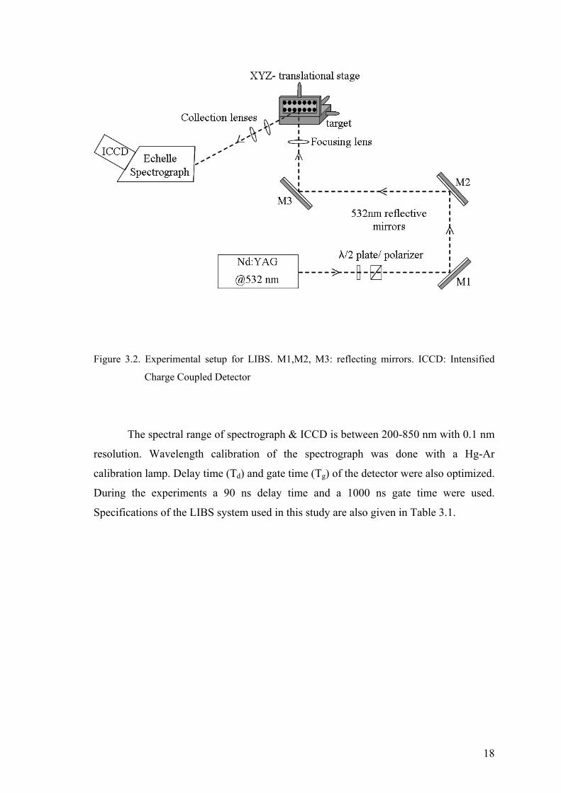
18
Figure 3.2. Experimental setup for LIBS. M1,M2, M3: reflecting mirrors. ICCD: Intensified
Charge Coupled Detector
The spectral range of spectrograph & ICCD is between 200-850 nm with 0.1 nm
resolution. Wavelength calibration of the spectrograph was done with a Hg-Ar
calibration lamp. Delay time (Td) and gate time (Tg) of the detector were also optimized.
During the experiments a 90 ns delay time and a 1000 ns gate time were used.
Specifications of the LIBS system used in this study are also given in Table 3.1.
19
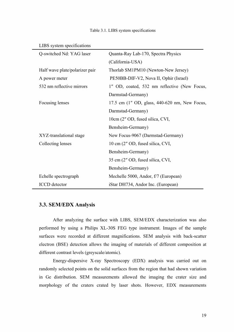
Table 3.1. LIBS system specifications
LIBS system specifications
Q-switched Nd: YAG laser Quanta-Ray Lab-170, Spectra Physics
(California-USA)
Half wave plate/polarizer pair Thorlab SM1PM10 (Newton-New Jersey)
A power meter PE50BB-DIF-V2, Nova II, Ophir (Israel)
532 nm reflective mirrors 1″ OD, coated, 532 nm reflective (New Focus,
Darmstad-Germany)
Focusing lenses 17.5 cm (1″ OD, glass, 440-620 nm, New Focus,
Darmstad-Germany)
10cm (2″ OD, fused silica, CVI,
Bensheim-Germany)
XYZ-translational stage New Focus-9067 (Darmstad-Germany)
Collecting lenses 10 cm (2″ OD, fused silica, CVI,
Bensheim-Germany)
35 cm (2″ OD, fused silica, CVI,
Bensheim-Germany)
Echelle spectrograph Mechelle 5000, Andor, f/7 (European)
ICCD detector iStar DH734, Andor Inc. (European)
3.3. SEM/EDX Analysis
After analyzing the surface with LIBS, SEM/EDX characterization was also
performed by using a Philips XL-30S FEG type instrument. Images of the sample
surfaces were recorded at different magnifications. SEM analysis with back-scatter
electron (BSE) detection allows the imaging of materials of different composition at
different contrast levels (greyscale/atomic).
Energy-dispersive X-ray Spectroscopy (EDX) analysis was carried out on
randomly selected points on the solid surfaces from the region that had shown variation
in Ge distribution. SEM measurements allowed the imaging the crater size and
morphology of the craters crated by laser shots. However, EDX measurements

20
permitted the identification of atomic compositions (in atomic percents) of species on
the solid samples.
3.4. AFM Analysis
The depth of craters was measured using a Multimode SPM, Nanoscope IV
Digital Instrument device type AFM. Measurements were done in contact mode.
Sample areas of about 1 cm x 1 cm were used.
21
CHAPTER 4
RESULTS AND DISCUSSION
4.1. Spectral Analysis by LIBS
In this thesis study, a LIBS system was constructed and applied for spectral
compositional analysis of solid samples at İYTE. For that purpose, spectral analysis of
some solid surfaces, such as Al, Cu, pure silicon wafer and Ge implanted siliconoxide
have been performed.
For qualitative analysis by LIBS, selection of the proper emission line to be
used for the identification of each element, is important. For this purpose National
Institute of Standards and Technology, NIST Electronic Database were used (NIST
2007) A list of the most intense emission lines observed from Al, Cu, Si and Ge is given
in Table 4.1.
Table 4.1. Spectral emission wavelengths of materials used
(Source: NIST)
Element Wavelength (nm) Element Wavelength (nm)
Si (I∗) 251.61 Cu (I) 324.75
Si (I) 288.15 Cu (I) 324.89
Si (II) 385.60 Cu (I) 427.51
Si (II) 386.26 Cu (I) 465.11
Si (I) 390.55 Cu (I) 515.32
Si (II) 412.80 Cu (I) 521.82
Si (II) 413.08 Al (I) 309.28
Ge (I) 303.91 Al (I) 309.47
Ge (I) 326.95 Al (I) 394.58
Ge (I) 422.66 Al (I) 396.34 ∗ (I) corresponds to neutral emission lines of elements. Whereas (II) and (III) represents
ionic and molecular species, respectively.
22
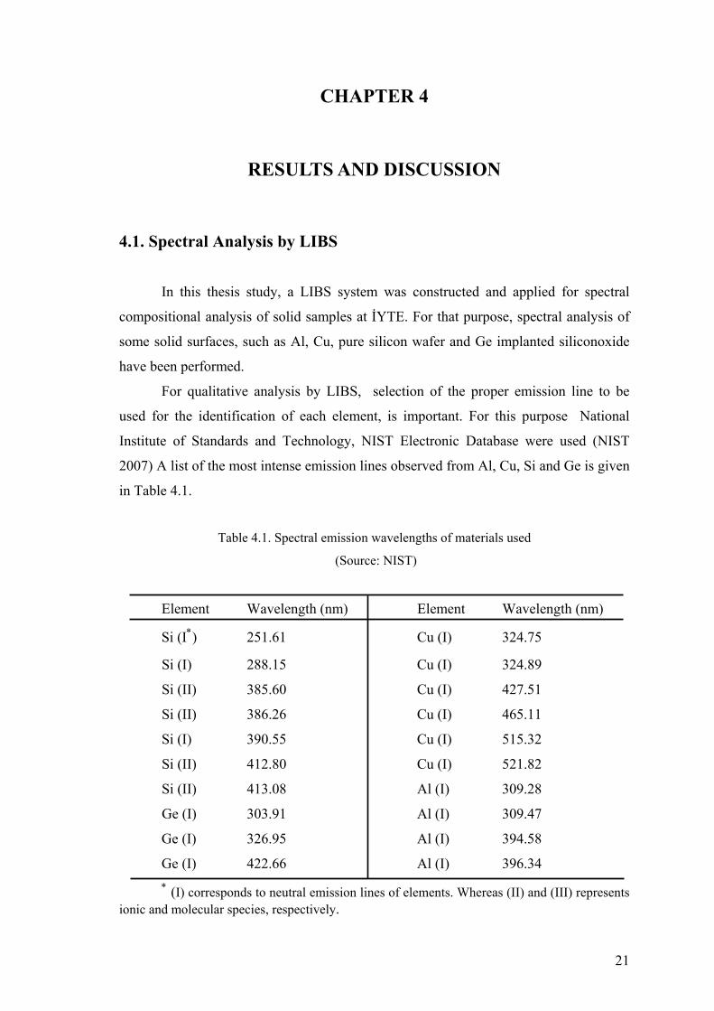
LIBS emission spectra obtained from Al and Cu targets within a wide spectral
range (250-850 nm) are shown in Figure 4.1 and Figure 4.2, respectively. The inset of
each figure shows some prominent lines in detail. Al lines have been measured by using
1.206 mJ/pulse laser energy while 0.983 mJ/pulse laser energy was used for the
observation of Cu lines. The spectra were obtained by accumulation of 10 repetetive
laser pulses.
In Figure 4.3 emission lines from pure silicon wafer are shown. Spectra was
taken with 0.768 mJ/pulse laser energy and a 10 cm focal length lens was used for
focusing the beam. The Si-288.15 nm and Si-390.55 nm lines were clearly observed
from a single laser shot at 90 ns delay time and 1000 ns gate time.
A Ge-implanted Si wafer surface was also analyzed using LIBS. Figure 4.4
represents the observed Si and Ge lines from a single laser shot with an energy of
1.726 mJ/pulse. Germanium lines observed at Ge (I)-303.91 nm and Ge (I)-326.95 nm
have apparently lower signal intensities than those from the silicon matrix lines
Si (I) 288.15 and Si (I) 390.55 nm due to the presence of Ge ions with an implantation
dose of 1 x 10¹⁷ ions/cm2.
23
F
igur
e 4.
1. T
ypic
al L
IBS
emis
sion
spec
trum
of A
l tar
get.
1.20
6 m
J/pu
lse
lase
r ene
rgy
was
use
d an
d 10
shot
acc
umul
atio
n w
as p
erfo
rmed
331
030
8
Al (
I)
309.
28 n
m
Al (
I)
309.
47 n
m
Al (
I)
394.
58 n
m
Al (
I)
396.
34 n
m
39
5
6000
5000
4000
3000
2000
1000 0
Relative Signal Intensity
420
400
380
360
340
320
300
280
Wav
eleng
th (n
m)

24
Fi
gure
4.2
. Typ
ical
LIB
S em
issi
on sp
ectru
m o
f Cu
targ
et. 0
.983
mJ/
puls
e. F
l=17
,5 c
m, 1
0 ac
cum
ulat
iıon
3500
3000
2500
2000
1500
1000 50
0 0
Relative Signal Intensity
550
500
450
400
350
300
Wav
elen
gth
(nm
)
428
426
466
465
520
515
326
325
324
Cu
(I)
324.
75 n
m
Cu
(I)
324.
89 n
m
Cu
(I)
427.
51 n
m
Cu
(I)
465.
11 n
m
Cu
(I)
515.
32 n
m
Cu
(I)
521.
82 n
m

25
Figu
re 4
.3. T
ypic
al L
IBS
emis
sion
spec
trum
of a
pur
e si
licon
waf
er
Si (I
) 28
8.15
nm
29
02
89
28
82
87
28
6
Si (I
) 39
0.55
nm
20 15 10 5 0
Relative Signal Intensity (x103 )
400
350
300
250
Wav
elen
gth
(nm
)
39
23
90
38
8

26
Figu
re 4
.4. T
ypic
al L
IBS
emis
sion
spec
trum
of G
e im
plan
ted
silic
on w
afer
hav
ing
an im
plan
tatio
n do
se o
f 1x
1017
ion/
cm2
Si (I
) 28
8.15
nm
30
43
03
()
32
73
26
Wl
th(
Ge
(I)
326.
95 n
m
Ge
(I)
303.
91 n
m
Si (I
) 39
0.55
nm
20 15 10 5 0
Relative Signal Intensity (x103 )
400
350
300
250
Wav
elen
gth
(nm
)

27
4.2. Signal Optimization
Line emission intensities from the luminous plasma were improved by several
signal optimization procedures, such as lens to sample distance, laser energy and the
crater size. Time resolution experiments were also performed for 2-D surface and depth
profiling analyses.
4.2.1. Focusing Lens to Sample Distance Adjustment
When 2-D compositional mapping analysis is uesed, the smallest possible crater
size is required for the best lateral resolution. The minimum spot size on the surface is
obtained at the focal point of the lens used. Thus, the distance between focusing lens
and sample surface is adjusted to obtain the smallest crater. A micrometer was used to
optimize the distance between focusing lens and sample surface. Figure 4.5 reprents the
optical microscope images of the craters produced with 17.5 cm focusing lens and
single laser pulses of 418 μJ/pulse energy was used. The smallest crater size of 33.88
μm was obtained nearly at the focal point of the lens.
Figure 4.5. Optical microscope images for focusing lens to sample distance adjustment with a
17.5 cm focusing lens and 418 μJ/pulse laser energies on a pure silicon surface,
single laser pulses were used
Figure 4.5 shows the variation of LIBS signal intensity with respect to lens
position. Normally signal increases as focal position is approached; however, the
highest LIBS signal intensity does not always necessarily correspond to the smallest
crater size. Therefore, there occurs a compromising condition between the detection
limit and the lateral resolution.
Focal point Out of focus Out of focus
28
On the other hand, in depth profiling analysis, better depth resolution is achieved
from craters with the smallest depth. Therefore, the condition that produces the smallest
possible crater having the smallest depth with a reasonable LIBS signal was selected for
three dimensional (3-D) microanalysis of the surfaces.
4.2.2. Time Resolution
Time resolved spectroscopic measurements were performed in order to find the
optimal time window for Ge signal intensity at 303.9 nm by imaging the whole plasma
on the entrance slit of the spectrograph. Single shot LIBS spectra of Ge-implanted
silicon oxide having an implantation dose of 1x1017 cm-2, showing the most relevant
emission lines, are given in Figure 4.6. The intensities of the ionic and neutral lines of
Si and Ge were measured with a time-gate of 1µs, at five different gate delay
times: 0, 50, 100, 200 and 400 ns.
Relative signal intensities from the ionic lines of Si (II) at 385.6 nm and
413.11 nm decreased as the gate delay time was increased and disappeared after 200 ns.
There was no ionic line emission detected from Ge within this spectral range under
these experimental conditions. However, the maximum emission signal from the neutral
emission lines of Ge(I) at 303.9 nm and Ge(I) at 326.95 nm were observed after 100 ns
delay time with respect to the laser pulse. Strong emission lines from the neutral Si(I) at
288.15 and 390.57 nm were relatively constant up to delay time of 200 ns after which
they decreased. Therefore, experiments were conducted with 90 ns delay and 1µs gate
time, where maximum Ge line emission observed, for the rest of the study.
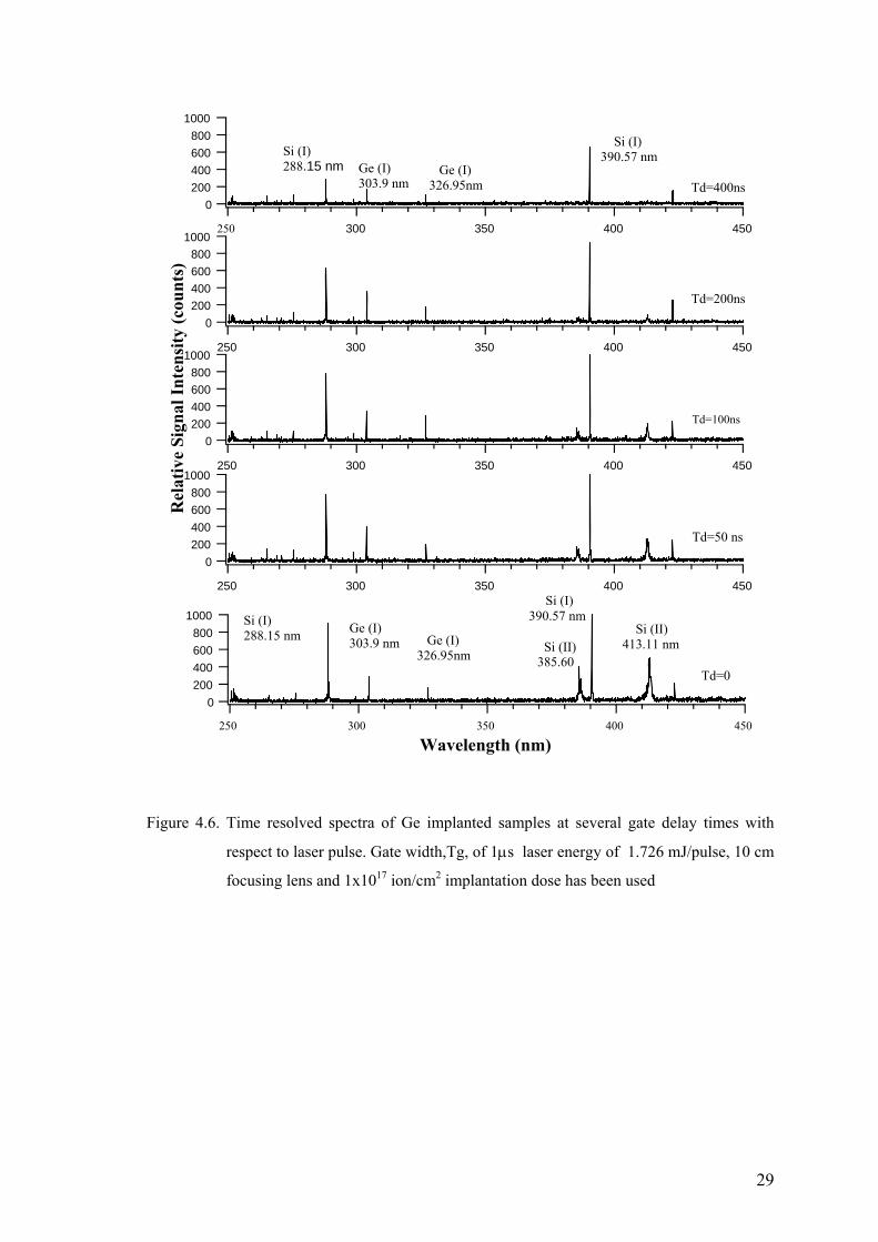
29
Figure 4.6. Time resolved spectra of Ge implanted samples at several gate delay times with
respect to laser pulse. Gate width,Tg, of 1μs laser energy of 1.726 mJ/pulse, 10 cm
focusing lens and 1x10¹⁷ ion/cm2 implantation dose has been used
1000 800600400200
0 450400 350300250
1000 800600400200
0 450400 350300250
1000 800600400200
0 450400 350300250
1000 800 600 400 200
0
450400350300250
Si (I)288.15 nm Ge (I)
303.9 nm Ge (I) 326.95nm
Si (I) 390.57 nm
Wavelength (nm)
Rel
ativ
e Si
gnal
Inte
nsity
(cou
nts)
Td=400ns
Td=100ns
Td=50 ns
Td=0
Si (I)288.15 nm Ge (I)
303.9 nm Ge (I) 326.95nm
Si (I) 390.57 nm
Si (II) 413.11 nm
1000 800600400200
0 450400 350300250
Si (II)385.60
Td=200ns
30
4.2.3. Germanium Signal Intensity and Implantation Dose
Figure 4.7. Germanium growth curves for Ge (303.9 nm) line, normalized to the 288.15 nm and
390.5 nm Si lines
In order to observe the variation of Ge signal intensity by LIBS with respect to
implantation dose, four samples of different implantation dose were used. Ge/Si line
intensity ratios plotted against the different Ge implantation doses are shown where the
Ge (303.9 nm) line is normalized with respect to neutral Si (288.15 nm and 90.56 nm)
lines (Figure 4.7). Each point in the figure represents the average of ten separate single
shot samplings from the central part of the implanted region in which a more
homogenous distribution exists. Line intensities were obtained from the peak area
measurements using a laser energy of 0.69 mJ/pulse. It can be seen from the figure that
the normalized Ge intensity exhibits a linear trend with respect to implantation dose
with correletaion coefficients of R2=0.989 and R2 = 0.995, when normalized to the
Si- 288.15 nm and 390.5 nm line emissions, respectively. The percent relative standard
deviation (% RSD) of the measurements ranged from 10–25% and relatively high
R2= 0,9958
R2=0,9899
0
0,05
0,1
0,15
0,2
0,25
0,3
0 0,5 1 1,5 2
Ge/
Si (2
88.1
5 nm
) Int
ensi
ty
0
0,05
0,1
0,15
0,2
Ge/Si (390.55 nm
) Intensity
Ge/Si (288.15 nm)
Ge/Si (390.55 nm)
Ge Implantation Dose (x 10 17 cm-2)

31
regression constant values indicated the possibility of semi-quantitative analysis of ion
implanted surfaces by LIBS.
4.2.4. Effect of Laser Energy
When nanosecond laser pulses are focused onto a target surface, the absorbed
energy heats up the target to the melting point and then to the vaporization temperature.
The power density is high enough that melted material is ejected due to the plasma
pressure, with plasma plume expanding into the ambient atmosphere. The ablated
amount from the surface is largely dependent on the incident laser energy.
The energy of the laser was tuned by using a half wave plate/polarizer pair and
plasma emission was collected using a side-viewing configuration, by imaging the
plasma onto the entrance slit of the spectrograph. The effect of laser energy on laser
induced plasma emission intensity is given in Figure 4.8. Here, spectra from the pure
silicon wafer were recorded within the 250-850 nm spectral regions for energies of
56 µJ - 1.7 mJ/pulse. This energy range corresponds to 0.38 GW/cm2 – 11.5 GW/cm2
irradiance values for crater sizes of 43 µm. The diameter of the focused beam size,
d, was calculated from the equation (Laserna 2004);
d= 2.44*λ*f / D (1-1)
where λ is the laser wavelength (532 nm), f is the focal length of the lens (100 mm) and
D is the diameter of the collimated laser beam (3 mm, after aperture).
A time delay of 90 ns and gate width of 1µs gave the maximum LIBS signal for
the Si lines. After that, 90 ns and gate width of 1µs were used in all experiments. Peak
areas calculated from three separate single shot measurements at each laser energy were
used to construct the figure for neutral Si (I) lines at 288.15 nm and 390.5 nm
(Figure 4.8).

32
Figure 4.8. Relative signal intensities of Si–288.15 nm and Si–390.55 nm at different laser
energy. The pure silicon wafer has been analyzed with a 10 cm focusing lens and
one single laser shot
Generally signal intensity increases as the laser energy increases. For both
Si-288.15 nm and Si-390.55 nm lines signal intensity deviates from linearity at high
energies (>50 μJ/pulse), which could be attributed to laser beam absorption by the
plasma above the target surface known as plasma shielding (Aguilera 1998, Russo
2004). However, in the region between 56 μJ/pulse and 80 μJ/pulse 2 different regions
were observed. Initially a sharp increase in signal intensity was observed between
56-60 µJ/pulse energy, then it slows down and bends between 60- 80 µJ energy range.
Then, a second increase in signal intensity between 80-90 µJ/pulse energy is observed.
Finally, signal emission rolls off drastically, after 90 µJ/pulse laser energy. This
variation in signal intensity within this power regime (0.38 GW/cm2 – 11.5 GW/cm2)
could be explained by the evolution of the plasma at different irradiance
regimes (Root 1989, Yalcın 1999).
0
100
200
300
400
500
600
700
800
900
1000
0 30 60 90 120 150 180
Rel
ativ
e Si
gnal
Inte
nsity
(x10
3 ) Si-288.15 nmSi-390.55 nm
Laser Energy (μJ/pulse)
33
Two dimensional (2-D) scanning analysis measurements were performed at low
pulse energies of between 56-250 µJ where the signal emission is mostly due to the
neutral and singly ionized atoms. In this regime, the plasma has a low temperature and
low electron density and is thin enough to allow the laser radiation to penetrate for
proportional ablation (Yalcin, et al. 1999)
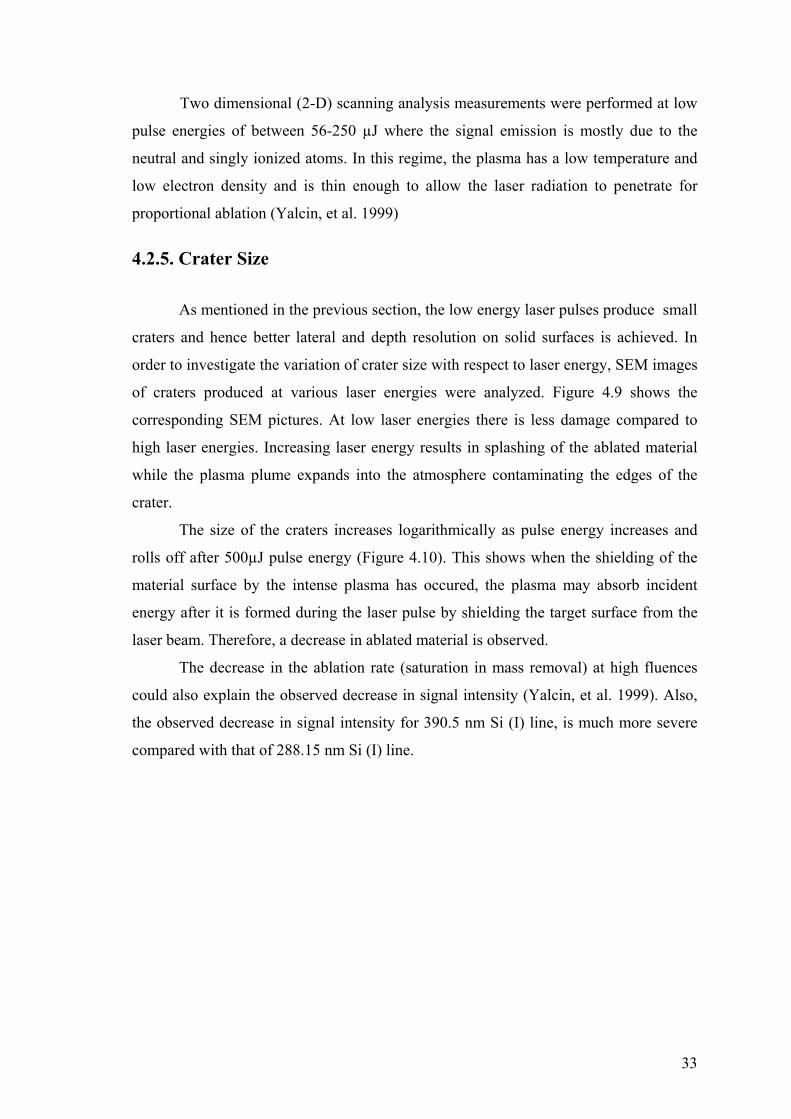
4.2.5. Crater Size
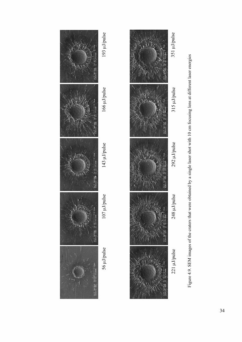
As mentioned in the previous section, the low energy laser pulses produce small
craters and hence better lateral and depth resolution on solid surfaces is achieved. In
order to investigate the variation of crater size with respect to laser energy, SEM images
of craters produced at various laser energies were analyzed. Figure 4.9 shows the
corresponding SEM pictures. At low laser energies there is less damage compared to
high laser energies. Increasing laser energy results in splashing of the ablated material
while the plasma plume expands into the atmosphere contaminating the edges of the
crater.
The size of the craters increases logarithmically as pulse energy increases and
rolls off after 500µJ pulse energy (Figure 4.10). This shows when the shielding of the
material surface by the intense plasma has occured, the plasma may absorb incident
energy after it is formed during the laser pulse by shielding the target surface from the
laser beam. Therefore, a decrease in ablated material is observed.
The decrease in the ablation rate (saturation in mass removal) at high fluences
could also explain the observed decrease in signal intensity (Yalcin, et al. 1999). Also,
the observed decrease in signal intensity for 390.5 nm Si (I) line, is much more severe
compared with that of 288.15 nm Si (I) line.
34
Figu
re 4
.9. S
EM im
ages
of t
he c
rate
rs th
at w
ere
obta
ined
by
a si
ngle
lase
r sho
t with
10
cm fo
cusi
ng le
ns a
t diff
eren
t las
er e
nerg
ies
56 μ
J/pu
lse
107
μJ/p
ulse
14
3 μJ
/pul
se
166
μJ/p
ulse
19
3 μJ
/pul
se
221
μJ/p
ulse
24
8 μJ
/pul
se
292
μJ/p
ulse
31
5 μJ
/pul
se
351
μJ/p
ulse

35
Figure 4.10. Relationship of laser energy to crater size. The pure silicon wafer has been
analyzed with a 10 cm focusing lens and a single laser shot at each laser energy
4.3. Two Dimensional (2-D) Compositional Mapping
4.3.1. LIBS Analysis
In the case of 2-D scanning analysis of the surfaces for determination of the
compositional variation of the element of interest, the lateral resolution is the main issue
to be considered. High lateral resolution can be obtained by using the smallest focal
spot possible and the lowest pulse energy, which gives rise to a detectable LIBS signal
(Bette and Noll 2003).
Low energy laser pulses can provide high lateral resolution at the expense of
sensitivity. Figure 4.11.a shows an SEM photomicrograph of the 2-D scanning analysis
of the Ge-ion implanted Si wafer surface within an area of 1.6 x 12 mm . Sixty craters
have been created on each of 9 rows with 5 laser shots each, at a laser energy of 250 μJ/
pulse. All representative image of a single crater formed by 5 consecutive laser shots is
given in Figure 4.11.b.
0
20
40
60 80
100
120 140
0 50 100 150 200 250Laser Energy (μJ/pulse)
Cra
ter
Size
(μm
)
ExperimentalLogarithmic

36
(a)
(b)
Figure 4.11. (a) SEM image of the Ge-ion implanted Si wafer within an area of 1.8 x 12 mm2
60 craters have been constructed on each 9 rows with 5 laser shot by a laser energy
250 μJ/ pulse (b) The image of a single crater formed by 5 consecutive laser shots
When a 3-D graph of this scanning was plotted against the Ge signal intensity at
Ge (I) 303.9 nm (Figure 4.12), the variation in Ge intensity can be observed.
The scanning was begun from a point on which there was no implanted Ge ion present.
Laser pulses of 250 µJ/ pulse energy were used on samples having a Ge implantation
dose of 6x1016 cm-2. A 12x1.6 mm (x:y) sampling area starting from the outer
edge representing low Ge concentration diffused out of the mechanical mask,
(see Figure 3.1.b) to the center of the implanted region was scanned at 200 micrometer

37
intervals. There were nine rows of sampling on the vertical (y) axis, each containing 60
sequentially formed craters. Here, only 4 of the 9 series in vertical axis are shown in the
Figure 4.12.a for clarity. LIBS spectral measurements revealed low Ge concentrations at
the edge and higher concentrations toward the center of the implanted region.
The distribution shown in the forefront Figure 4.12.b was obtained from the non-
implanted region of the SiO2 surface (blank), whereas the one at the back was obtained
from the implanted region. Lower pulse energies of 69 microjoules enabled the
sampling of 50 micrometer intervals. The same high noise characteristics observed for
both implanted and non-implanted regions can be attributed to the use of the ICCD
detector at high gain settings.

38
0
20x103
40x103
60x103
80x103
100x103
120x103
02
46
810
1214
0.1
0.2
0.3
0.4
0.5
0.6
0.70.8
0.9
Rel
ativ
e G
e In
tens
ity
(C
ount
s)
Position x-axis
(mm)
Position x-axis
(mm
)
(a)
0
200
400
600
800
1000
05
1015
2025
0.1
0.2
0.3
0.4
0.5
0.6
Rel
ativ
e G
e In
tens
ity
(Cou
nts)
Position x-axis
(mm)
Position y-axis
(mm
)
(b)
Figure 4.12. Ge ion distribution on implanted SiO2 surfaces. (a) 250 μJ/pulse energy, 200 μm
sampling intervals in both (x:y) direction, (b) 69 μJ/ pulse energy, 50 μm
sampling intervals, from implanted region (back) and non-implanted region
(front)
39
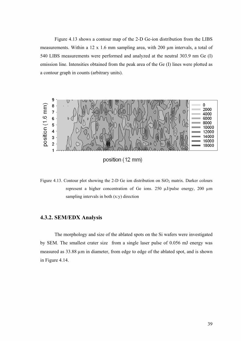
Figure 4.13 shows a contour map of the 2-D Ge-ion distribution from the LIBS
measurements. Within a 12 x 1.6 mm sampling area, with 200 µm intervals, a total of
540 LIBS measurements were performed and analyzed at the neutral 303.9 nm Ge (I)
emission line. Intensities obtained from the peak area of the Ge (I) lines were plotted as
a contour graph in counts (arbitrary units).
Figure 4.13. Contour plot showing the 2-D Ge ion distribution on SiO2 matrix. Darker colours
represent a higher concentration of Ge ions. 250 μJ/pulse energy, 200 μm
sampling intervals in both (x:y) direction
4.3.2. SEM/EDX Analysis
The morphology and size of the ablated spots on the Si wafers were investigated
by SEM. The smallest crater size from a single laser pulse of 0.056 mJ energy was
measured as 33.88 μm in diameter, from edge to edge of the ablated spot, and is shown
in Figure 4.14.
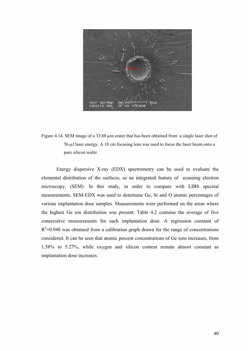
40
Figure 4.14. SEM image of a 33.88 μm crater that has been obtained from a single laser shot of
56 μJ laser energy. A 10 cm focusing lens was used to focus the laser beam onto a
pure silicon wafer
Energy dispersive X-ray (EDX) spectrometry can be used to evaluate the
elemental distribution of the surfaces, as an integrated feature of scanning electron
microscopy, (SEM). In this study, in order to compare with LIBS spectral
measurements, SEM-EDX was used to determine Ge, Si and O atomic percentages of
various implantation dose samples. Measurements were performed on the areas where
the highest Ge ion distribution was present. Table 4.2 contains the average of five
consecutive measurements for each implantation dose. A regression constant of
R2=0.948 was obtained from a calibration graph drawn for the range of concentrations
considered. It can be seen that atomic percent concentrations of Ge ions increases, from
1.58% to 5.27%, while oxygen and silicon content remain almost constant as
implantation dose increases.

41
Table 4.2. SEM-EDX measurements, atomic percent values for Si, Ge and O atoms at
different implantation doses. Data were obtained from five different measurements
(R2 = 0.948)
Implantation
Dose
Atomic %
Oxygen
Atomic %
Germanium
Atomic %
Silicon
3.0 x 10¹⁶ 32.77 1.58 65.64
6.0 x 10¹⁶ 30.77 2.36 66.87
1.0 x 10¹⁷ 37.87 4.49 57.64
1.5 x 10¹⁷ 32.56 5.27 62.18
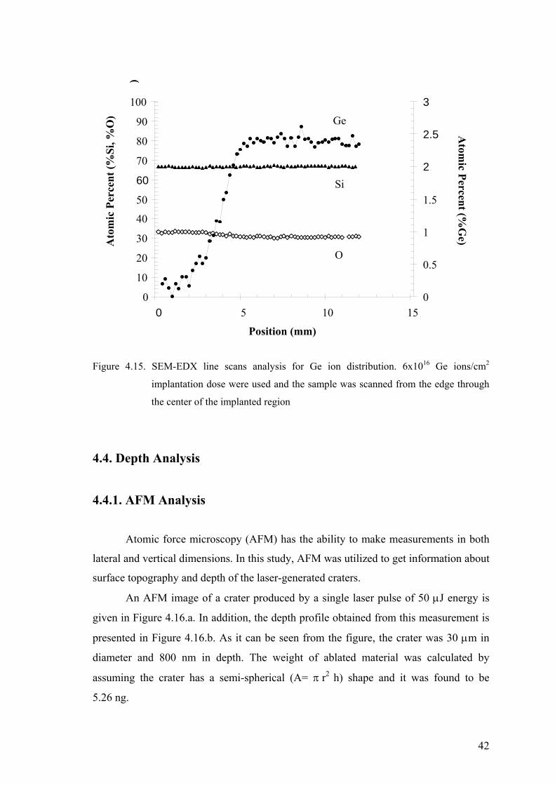
In order to compare 2-D scanning LIBS analysis with EDX, line scan analysis of
implanted surfaces by SEM-EDX was also performed. Lateral analysis by EDX was
performed by starting from the edge to the center of the implanted region in a way
similar to how it had been done for LIBS measurements. A sample with a
6 x10¹⁶ Ge ions/cm2 implantation dose was used for line scan analysis and elemental
compositions of Si, O, and Ge ions were obtained.
Figure 4.15 represents the elemental distribution of Si, Ge and O atoms
measured at 60 different positions at about 200 μm intervals, along the horizontal axis
(x-axis). In this figure, the Ge atomic percentage values obtained from EDX
measurements are shown on the right y-axis while Si and O were on the left. It was
observed that Ge ion concentration changes, laterally, from (0.5-2.8) % (atomic) for a
sample with 6x1016 cm-2 implantation dose. This range was estimated as (0.2-1.58) %
when 3x10¹⁶ Ge ions/cm2 implantation dose of a sample was used. Each point in the
figure is the average of 5 consecutive measurements. It can be seen that the atomic
percent concentrations of Ge ions increases while oxygen and silicon remains almost
constant as implantation dose increases.
42
Figure 4.15. SEM-EDX line scans analysis for Ge ion distribution. 6x10¹⁶ Ge ions/cm2
implantation dose were used and the sample was scanned from the edge through
the center of the implanted region
4.4. Depth Analysis
4.4.1. AFM Analysis
Atomic force microscopy (AFM) has the ability to make measurements in both
lateral and vertical dimensions. In this study, AFM was utilized to get information about
surface topography and depth of the laser-generated craters.
An AFM image of a crater produced by a single laser pulse of 50 μJ energy is
given in Figure 4.16.a. In addition, the depth profile obtained from this measurement is
presented in Figure 4.16.b. As it can be seen from the figure, the crater was 30 μm in
diameter and 800 nm in depth. The weight of ablated material was calculated by
assuming the crater has a semi-spherical (A= π r2 h) shape and it was found to be
5.26 ng.
0
10
20
30
40
50
60
70
80
90
100
0 5 10 15
Position (mm)
Ato
mic
Per
cent
(%Si
, %O
)
0
0.5
1
1.5
2
2.5
3 A
tomic Percent (%
Ge)
O
0
10
20
30
40
50
60
70
80
90
100
0 5 10 15
Position (mm)
Ato
mic
Per
cent
(%Si
, %O
)
0
0.5
1
1.5
2
2.5
3 A
tomic Percent (%
Ge)
Ge
Si
O

43
(a)
(b)
Figure 4.16. (a) Atomic force microscope image and (b) depth profile of a crater formed from
a single laser shot with 50 µJ/ pulse energy
-1
-0.5
0
0.5
1
1.5
-2 4 10 16 22 28 34
Distance (μm)
Hei
ght (
μm)
44
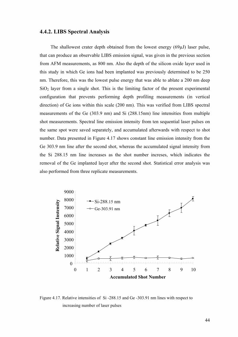
4.4.2. LIBS Spectral Analysis
The shallowest crater depth obtained from the lowest energy (69µJ) laser pulse,
that can produce an observable LIBS emission signal, was given in the previous section
from AFM measurements, as 800 nm. Also the depth of the silicon oxide layer used in
this study in which Ge ions had been implanted was previously determined to be 250
nm. Therefore, this was the lowest pulse energy that was able to ablate a 200 nm deep
SiO2 layer from a single shot. This is the limiting factor of the present experimental
configuration that prevents performing depth profiling measurements (in vertical
direction) of Ge ions within this scale (200 nm). This was verified from LIBS spectral
measurements of the Ge (303.9 nm) and Si (288.15nm) line intensities from multiple
shot measurements. Spectral line emission intensity from ten sequential laser pulses on
the same spot were saved separately, and accumulated afterwards with respect to shot
number. Data presented in Figure 4.17 shows constant line emission intensity from the
Ge 303.9 nm line after the second shot, whereas the accumulated signal intensity from
the Si 288.15 nm line increases as the shot number increses, which indicates the
removal of the Ge implanted layer after the second shot. Statistical error analysis was
also performed from three replicate measurements.
Figure 4.17. Relative intensities of Si -288.15 and Ge -303.91 nm lines with respect to
increasing number of laser pulses
0
1000
2000
3000
4000
5000
6000
7000
8000
9000
0 1 2 3 4 5 6 7 8 9 10 Accumulated Shot Number
Rel
ativ
e Si
gnal
Inst
ensi
ty Si-288.15 nmGe-303.91 nm

45
CHAPTER 5
CONCLUSIONS
LIBS has been demonstrated as a semi-quantitative spectral analysis technique
for 2-D analysis of Ge-implanted silicon oxide surfaces. A typical LIBS optical system
was designed, constructed from its commercially available parts for solids analysis at
İYTE. Germanium -samples with implantation doses of between 1x10¹⁶-1.5x10¹⁷
ions/cm2, prepared by the method of ion implantation were analyzed for the the
assessment of the LIBS system constructed.
LIBS spectral measurements indicate 50 µm lateral and 800 nm depth resolution
from single shot measurements. SEM-EDX analysis has been used to correlate semi-
quantitative LIBS spectral measurements. It has been shown that LIBS has the
capability to detect atomic concentrations of Ge ions lower than 0.2% in the Si/SiO2
matrices.
For two dimensional (2-D) scanning analysis LIBS presents advantages over
SEM-EDX analysis in terms of scan time, but has similarities in both accuracy and
sensitivity. It can be concluded that lateral and depth resolution can be further improved
by the establishment of tighter focusing of the laser beam and gentler ablation
conditions with the use of less energetic laser pulses.
46
REFERENCES
Aguilera, J.A., Aragon, C., Penalba, F., 1998. Plasma shielding effect in laser ablation of metallic samples and its influence on LIBS analysis. Applied Surface Science 127: 309-314.
Andor Technology, Digital Camera Fundamentals Rank Top 2 http://www.andor.com/library/digital_cameras
(accessed September 30, 2007).
Bärsch, N., Körber, K., Ostendorf, A., Tönshoff, K.H., 1996. Ablation and cutting of planar silicon devices using femtosecond laser pulses. Applied Physics 77(A):237-242.
Bette, H., M.F., Noll, R., 2003. High-speed scanning laser-induced breakdown spectroscopy at 1000 Hz with single pulse evaluation for the detection of inclusions in steel. Applied Physics 37:1281– 1288.
Brennetot, R., Lacour, J.L., Vors, E., Rıvoallan, A., Vaılhen, D., Maurıce, S., 2003. Mars Analysis by Laser-Induced Breakdown Spectroscopy (MALIS): Influence of Mars Atmosphere on Plasma Emission and Study of Factors Influencing Plasma Emission with the use of Doehlert Designs. Applied Spectroscopy 57:744–752.
Bustamante, M.F., Rinaldi, C.A. and Ferrero, J.C., 2002. Laser induced breakdown spectroscopy characterization of Ca in a soil depth profile Spectrochimica Acta Part B 57:303–309.
Cravetchi, I.V., Taschuk, M.T., Tsui, Y.Y., Fedosejevs, R., 2004. Scanning microanalysis of Al alloys by laser-induced breakdown spectroscopy Spectrochimica Acta Part B 59:1439–1450.
Dixon, P.B., Hahn, D.W., 2005. Feasibility of detection and ıdentification of ındividual bioaerosols using laser-ınduced breakdown spectroscopy. Analytical Chemistry 77:631–638.
Dolores, R., Lasrena, J.J., 1998. Surface and tomographic distribution of carbon impurities in photonic-grade silicon using laser-induced breakdown spectrometry. Journal of Analytical Atomic Spectrometry 13:557–560.
García, C.C., Corral, M., Vadillo, J.M. and J. J. Laserna, 2000. Angle-Resolved Laser-Induced Breakdown Spectrometry for Depth Profiling of Coated Materials. Applied Spectroscopy 54:1027-1031.

47
Giakoumaki, A., Melessanaki, K., Anglos, D., 2007. Laser-induced breakdown spectroscopy (LIBS) in archaeological science applications and prospects. Analytical Bioanalytical Chemistry 387:749–760.
Gondal M.A., Hussain, T., Yamani, Z.H., Baig, M.A., 2006. The role of various binding materials for trace elemental analysis of powder samples using laser-induced breakdown spectroscopy. Talanta 72:642–649.
Häkkänen, H., Houni, J., Kaski, S., Korppi-Tommola, J.E.I., 2001. Analysis of paper by laser-induced plasma spectroscopy. Spectrochimica Acta Part B 56: 737-742.
Knight, A.K., Scherbarth, N.L., Cremers, D.A., Ferrıs, M.J., 2000. Characterization of Laser-Induced Breakdown Spectroscopy (LIBS) for Application to Space Exploration. Applied Spectroscopy 54:331–340.
Laserna, J.J., Vadillo, J.M., 2004. Laser-induced plasma spectrometry: truly a surface analytical tool. Spectrochimica Acta Part B 59:147–161.
Margetic, V., Bolshov, M., Stockhaus, A., Niemax, K., Hergenröder, R., 2001. Depth profiling of multi-layer samples using femtosecond laser ablation. Journal of Analytical Atomic Spectrometry 16:616-621.
Mateo, M. P., Nicolas, G., Pinon V. and A. Yanez, A., 2006. Improvements in depth profiling of thick samples by laser-induced breakdown spectroscopy using linear correlation. Surface Interface Analysis 38:941–948.
Mateo, M.P., Vadillo, J.M., Laserna, J.J., 2001. Irradiance-dependent depth profiling of layered materials using laser-induced plasma spectrometry. Journal of Analytical Atomic Spectrometry 16:1317-1321.
Milan, M., Lucena, P., Cabalin, L.M., Laserna, J.J., 1998. Depth Profiling of Phosphours in Photonic-Grade Silicon Using Laser-Induced Breakdown Spectrometry. Applied Spectroscopy 52:444-448.
Mirov S.B., Pitt, R.E., Dergachev, A., Lee, W., Martyshkin, D.V., Mirov, O.D., Randolph, J.J., DeLucasc, L.J., Brouillette, C.G., Basiev, T.T., Orlovskii, Y.V. Alimov, O.K., 1999. A novel laser breakdown spectrometer for environmental monitoring. Society of Photo-Optical Instrumentation Engineers 3855: 34–41.
NIST Atomic Spectra Database Lines Form
National Institue of Standards and Technology http://physics.nist.gov/PhysRefData/ASD/lines_form.html (accessed September 25, 2007).

48
Pronko, P.P., Dutta, S.K., Du, D., 1995. Thermophysical effects in laser processing of materials with picosecond and femtosecond pulses. Journal of Applied Physics 78:6233-6240.
Radziemski, L.J., Cremers, D.A., 1989. Handbook of Laser-Induced Breakdown Spectroscopy. New York: Marcel Dekker, Optical Engineering Series.
Rieger, G. W., Taschuk, M., Tsui, Y.Y., Fedosejevs, R., 2002. Laser Induced Breakdown Spectroscopy for Microanalysis Using Submillijoule UV Laser Pulses. Applied Spectroscopy 56:689-698.
Rimini, E., 1995. Ion Implantaion Basics to Device Fabrication. Boston: Kluwer
Academic Publishers. Root, R.G., 1989. Laser Induced Plasmas and Applications. New York: Marcel
Decker.
Rubin, L., Poate, J., 2003. Ion Implantation in Silicon Technology. New York: American Institute of Physics.
Russo, R.E., Mao, X.L., Liu, C., Gonzales, J., 2004. Laser assisted plasma spectrochemistry: laser ablation. Journal of Analytical Atomic Spectrometry 19:1084-1089.
Samek, O., Telle, H.H., Beddows, D.C.S., 2001. Laser-induced breakdown spectroscopy: a tool for real-time, in vitro and in vivo identification of carious teeth. BMC Oral Health 1(1)6831-1472.
Sauter, E.G., 1996. Nonlinear Optics. New York: John-Wiley.
Siegman, A. E., 1986. Lasers. California: Sausalito,University Science Books. Silfvast, W. T., 1996. Laser fundamentals. Cambridge; Cambridge unv. Press.
Skoog, D.A., Holler, and F.J., Nieman, T.A., eds. 1997. Principles of Instrumental Analysis. New: York Hardcover .
Skoog, M.D., West, D.M., and Holler, F.J., eds. 1997. Fundamentals of Analytical Chemistry. Florida: Harcourt Brace & Company.
Sneddon J., Thiem T.L., and Lee Y-III., eds. 1997. Lasers In Analytical Atomic Spectroscopy. New York: VCH Publishers.

49
Vadillo, J.M., Garcia, C.C., Palanco, S., and Laserna, J.J., eds. 1998. Nanometric range depth- resolved analysis of coated-steels using laser-induced breakdown spectrometry with a 308 nm collimated beam. Journal of Analytical Atomic Spectrometry 13:793-797.
Winefordner, J.D., Gornushkin, I.B., Correll, T., Gibb, E., Smith, B.W., Omenetto, N.,
2004. Comparing several atomic spectrometric methods to the super stars: special emphasis on laser induced breakdown spectrometry, LIBS, a future super star. Journal of Analytical Atomic Spectrometry 19:1061-1083.
Yalcin, S., Crosley, D.R., Smith, G.P., Faris, G.W., 1999. Influence of ambient
conditions on the laser air spark. Applied Physics 68:121-130.