Embed Size (px)
Citation preview

NanoscaleAdvances
PAPER
Ope
n A
cces
s A
rtic
le. P
ublis
hed
on 2
9 Ju
ne 2
020.
Dow
nloa
ded
on 2
/27/
2022
10:
33:2
3 A
M.
Thi
s ar
ticle
is li
cens
ed u
nder
a C
reat
ive
Com
mon
s A
ttrib
utio
n-N
onC
omm
erci
al 3
.0 U
npor
ted
Lic
ence
.
View Article OnlineView Journal | View Issue
Nanoscale laser-
aMinistry of Education (MOE) Key Labor
Instrumentation, College of Chemistry
University, Xiamen, 361005, China. E-mail:bState Key Laboratory of Marine Environme
361005, China
Cite this: Nanoscale Adv., 2020, 2,3983
Received 10th May 2020Accepted 27th June 2020
DOI: 10.1039/d0na00380h
rsc.li/nanoscale-advances
This journal is © The Royal Society o
induced breakdown spectroscopyimaging reveals chemical distribution withsubcellular resolution
Yifan Meng,a Chaohong Gao,a Zheng Lin,a Wei Hang *ab and Benli Huanga
Understanding chemical compositions is one of the most important parts in exploring the microscopic
world. As a simple method for elemental detection, laser-induced breakdown spectroscopy (LIBS) is
widely used in materials, geological and life science fields. However, due to the long-existing limitation
in spatial resolution, it is difficult for LIBS to play an analytical role in the field of micro-world. Herein, we
first report a reliable nanoscale resolution LIBS imaging technique by introducing a sampling laser with
a micro-lensed fiber. Through the emission enhancement using the double-pulse laser, we obtained the
spectral signal from a sampling crater of less than 500 nanometers in diameter, and visualized the
chemical distribution of the self-made grid sample, SIM chip and nano-particles in single cells. The
relative limits of detection (RLODs) of In and absolute limits of detection (ALODs) of Al can reach 0.6%
and 18.3 fg, respectively.
1. Introduction
With the development of analytical techniques, researchers aremore interested in imaging the chemical compositions ofdifferent regions of samples, rather than the compositions ofaveraging large areas.1–7 Due to advantages of high sensitivityand fast analysis speed, laser-induced breakdown spectroscopy(LIBS) plays an important role in elemental analysis.8–14
Furthermore, it has become one of the most attractive tech-nologies in the eld of elemental imaging.15–18 However, due tothe difficulty in reducing the sampling spot limited by thediffraction limit and lens aberration, it has been difficult toapply LIBS in the micro–nano scale analysis for a long time.19–23
This is one of the reasons that hinder the development of LIBSimaging in various microanalysis elds, such as nanomaterials,microstructure and single-cell analysis.
Recent decades have witnessed great efforts made by manyresearchers in improving the lateral resolution of LIBS to lowmicron or nanometer scales. Several groups have usedmicroscopeobjectives to generate a tightly focused laser beam, namely in themicro-LIBS (mLIBS), resulting in lateral resolutions down to a fewmicrons.24–26 Ultrafast lasers offer a number of advantages inmaterials processing such as high-energy ux and limited thermaleffects.27,28 Therefore, the use of femtosecond lasers in LIBS hasshown an increasing trend in recent years.29,30 In addition, a crater
atory of Spectrochemical Analysis and
and Chemical Engineering, Xiamen
ntal Science, Xiamen University, Xiamen
f Chemistry 2020
size smaller than the focused-beam spot size can be obtainedthrough adjusting the laser energy threshold for ablation, bytaking advantage of the Gaussian spatial distribution of laserbeams,31,32 which makes it possible to obtain submicron craters.21
Additionally, using a near-eld technique to avoid the diffractionlimit is also an effective strategy to improve the resolution of LIBS.Near-eld techniques can achieve locally conned nanometricillumination of aperture probes for scanning near-eld opticalmicroscopy (SNOM).33–36 Several papers concerning apertureSNOM LIBS were published, indicating that SNOM has thepotential to improve the lateral resolution of laser sampling,20,37–39
but unfortunately the elemental emission signal of nanoscalecraters has not been obtained. Another near eld technique is touse apertureless metal tips to enhance the local electromagneticeld for ablation at the apex when the tip is illuminated witha suitable laser and the apex is close enough to the samplesurface.40,41 Study has shown that this technique can be used forsubmicron resolution imaging analysis of conductor samples.42
Nevertheless, the increase of spatial resolution results in thedecrease of the ablated amount. For crater sizes smaller than�0.5 mm, measurement of spectral emission becomes difficultusing classical emission monitoring in the optical far-eld,creating a dilemma for the nanoscale LIBS imaging tech-nique.21 Therefore, for detecting weak signals, it is necessary toenhance and amplify the LIBS spectral emission. At present, re-excitation of plasma using a double-pulse laser is one of themain means for LIBS signal enhancement.43 The concept ofdouble-pulse LIBS was rst developed by Cremers et al. inablation of liquids in 1984,44 while Niemax et al. applied thistechnique in solid sample analysis for the rst time in 1991.45
Double-pulse LIBS devices have two main congurations, the
Nanoscale Adv., 2020, 2, 3983–3990 | 3983

Fig. 1 The NLP-based double-pulse LIBS imaging platform. (A)Workflow of the LIBS imaging system. (B) Detailed schematic diagramof the sampling area outlined by the dash-square in (A) with the opticalphotograph of NLP shown in the top right corner. (C) The focusingprinciple of the NLP.
Nanoscale Advances Paper
Ope
n A
cces
s A
rtic
le. P
ublis
hed
on 2
9 Ju
ne 2
020.
Dow
nloa
ded
on 2
/27/
2022
10:
33:2
3 A
M.
Thi
s ar
ticle
is li
cens
ed u
nder
a C
reat
ive
Com
mon
s A
ttrib
utio
n-N
onC
omm
erci
al 3
.0 U
npor
ted
Lic
ence
.View Article Online
collinear geometry and the orthogonal geometry.43 The collineargeometry is not suitable for high spatial resolution LIBSimaging because it will re-destroy the sample surface, while theorthogonal geometry is ideal for enhancing spectral emissionwithout compromising the spatial resolution achieved with therst laser. The combination of femtosecond and ultravioletnanosecond lasers is able to enhance the spectral emission of Siby several orders of magnitude with the ablated crater smallerthan 2 mm.46
Herein, we rst demonstrate a nano laser probe (NLP)-baseddouble-pulse LIBS imaging method by introducing the rstsampling laser with a single-mode micro-lensed ber andenhancing the spectral emission using a second laser on thepremise of obtaining nanoscale ablated craters. With this newnanoscale resolution LIBS imaging approach, we achieved thevisual observation of the serial number (Al line) on a chip and thedistribution of nanoparticles (InP) in a single cell. In addition, wealso examined the limit of detection (LOD) of this method whoserelative limits of detection (RLODs) and absolute limits of detec-tion (ALODs) for indium can reach 0.6% and 18.3 fg, respectively.
2. Experimental2.1 Preparation of the grid sample and SIM chip
The Al grid sample was prepared as follows. A 1000 lines perinch and 600 lines per inch copper grid (G1000HS andAG600HSS, Gilder Grids, England) was used to cover a smoothsilica substrate, respectively. A 200 nm thick Al cladding wascoated on a smooth silicon wafer with a magnetron sputteringsystem (Explorer 14, Denton Vacuum, NJ, USA). The grid wasremoved aer the Al cladding was coated in holes. The SIM chipsample was prepared as follows. The SIM card was soaked inacetone for 4 hours to remove the coating resin. The chip wasremoved with tweezers and ultrasonically cleaned with ethanol.
2.2 Cell culture
Cells were cultured and treated as follows. Cells were grown inDulbecco's Modied Eagle's Medium (DMEM, HyClone) sup-plemented with 10% (v/v) FBS, 1% penicillin, and 1% strepto-mycin (3 mg ml�1 NaHCO3 was needed for RAW 264.7). Cellswere seeded into 150 mm Falcon culture dishes andmaintainedby the addition of newmedia every 2–3 days. Quartz wafers sized1 � 1 cm2 were rinsed in HPLC-grade water and ethanol, andthen sterilized for the cell cultures. Subsequently, the quartzwafers were placed in a 6-well plate, and cells were seeded intothe wells at a cell density of 1 � 103–1 � 104 cells per well, andallowed to grow for 24 hours under constant conditions of 37 �Cand 5% CO2. Nanoparticles were added into each well witha concentration of 100 mmol L�1 and then cultured for 24 hours.Finally, the cells were dyed with Lyso-Tracker Red DND-99 for1 h.
2.3 Data analysis
The emission spectrum from each laser pulse was recordedusing the LightField program (Princeton Instruments, USA) andthen processed using a self-compiled program written in
3984 | Nanoscale Adv., 2020, 2, 3983–3990
LabVIEW (National Instruments, USA). LIBS images were con-structed using Surfer 9 soware (Golden Soware, Inc., USA). Allthe images were generated without the use of other imageprocessing steps, such as smoothing or interpolation.
2.4 NLP-based double-pulse LIBS imaging system
The NLP-based double-pulse LIBS imaging system includesa sequential control device, a femtosecond laser (515 nm forsampling, S-Pulse, Amplitude Systems, France) and a nano-second laser (266 nm for emission enhancement, Minilite-II,Continuum Inc., USA), a micro-lensed ber and laser couplingsystem, a sample stage, a vacuum chamber and a spectrometer
This journal is © The Royal Society of Chemistry 2020
Paper Nanoscale Advances
Ope
n A
cces
s A
rtic
le. P
ublis
hed
on 2
9 Ju
ne 2
020.
Dow
nloa
ded
on 2
/27/
2022
10:
33:2
3 A
M.
Thi
s ar
ticle
is li
cens
ed u
nder
a C
reat
ive
Com
mon
s A
ttrib
utio
n-N
onC
omm
erci
al 3
.0 U
npor
ted
Lic
ence
.View Article Online
(Model SP 2300i, Princeton Instruments, USA). The spectrom-eter has a scan range of 0–1400 nm and a wavelength accuracyof �0.2 nm, which is suitable for the experiment of nanoscalespatial resolution LIBS imaging. The workow is shown inFig. 1A. The whole imaging process is achieved using self-written soware with LabVIEW (National Instruments, USA).The delay generator (DG-645, Stanford Research Systems, USA)triggers the two laser beams and the spectrometer throughthree output channels, respectively. The interpulse delay of thetwo lasers and the detection delay of emICCD (PI-MAX 4,Princeton Instruments, USA) of the spectrometer can beadjusted precisely. To investigate the effect of different airpressure on spectral emission intensity, the sample stage isplaced in a vacuum chamber where the air pressure could becontrolled. The micro-lensed ber for sampling and the opticalber for signal collection are connected to the vacuum chamberthrough two vacuum feed-through anges, respectively. Thenanosecond laser is focused through the quartz window on theside of the vacuum chamber. Fig. 1B shows a schematicdiagram of the sampling area of the NLP-based double-pulseLIBS imaging device. To obtain a high-quality Gaussian beamand focus spots as small as possible, the NLP is made usinga pure silica single-mode ber (Nufern S460 HP, mode elddiameter ¼ 2.5 mm) and the radius of curvature of the microlens is designed to be 4.5 mm (Fig. 1C). Fixed on a one-dimensional micro positioner, the NLP focuses the femto-second laser on the sample surface with an optimal tip-surfacedistance of 9 mm. The plasma produced by the femtosecondlaser will be re-heated by the focused ultraviolet nanosecondlaser beam. To get the optimal spectral emission lines, the re-
Fig. 2 Optimization of gas pressure, interpulse delay and detection delapressure (A, from 1� 105 Pa to 5� 10�4 Pa), different interpulse delay (B, fns). The relationships of the signal-to-noise ratio (SNR) of spectral emissdetection delay (F).
This journal is © The Royal Society of Chemistry 2020
heating laser beam needs to be as close to the sample surfaceas possible. In this experiment, in consideration of the ber tipposition, the distance between the nanosecond laser andsample surface is set as 1 mm. The LIBS spectral emission iscollected using an optical ber (400 mm wide ber core,WYOPTICS, Shanghai, China) with a coupling lens (74UV withSMA 905 connector, WYOPTICS, Shanghai, China) and istransmitted to the spectrometer with a 2400 groove per mmgrating. The distance between the collection optics and samplesurface is set at 10 mm. With a CCD camera, we can observe thedistance between the ber tip and the sample surface, and theregion of interest (ROI) of the sample. With the closed-loop XYmicro positioner acting as the sample stage (SLC-1720, SmarActGmbH, Germany), imaging acquisition of the ROI can be con-ducted automatically by the LabVIEW program.
3. Results and discussion3.1 Optimization of the gas environment and delay time
Studies have shown that the spectral resolution of LIBS ob-tained under vacuum conditions is better than that underatmospheric pressure.42 When the pressure decreases, due tothe weakening of the plasma shielding effect and self-absorption effect, the signal intensity of the LIBS spectrumis increased.47,48 The low-pressure environment also resultsin higher spectral resolution, increased ablation and moreuniformly ablated craters.49 For high spatial resolutionimaging applications, the inuence of ambient air pressureon the weak spectral signal is more signicant. In addition,following its creation by the laser pulse, the plasma expands
y. The emission spectra of Al(I) at 394.4 nm and 396.1 nm at differentrom 0 ns to 2900 ns) and different detection delay (C, from 30 ns to 270ion of Al(I) at 396.1 nm at different pressure (D), interpulse delay (E) and
Nanoscale Adv., 2020, 2, 3983–3990 | 3985

Nanoscale Advances Paper
Ope
n A
cces
s A
rtic
le. P
ublis
hed
on 2
9 Ju
ne 2
020.
Dow
nloa
ded
on 2
/27/
2022
10:
33:2
3 A
M.
Thi
s ar
ticle
is li
cens
ed u
nder
a C
reat
ive
Com
mon
s A
ttrib
utio
n-N
onC
omm
erci
al 3
.0 U
npor
ted
Lic
ence
.View Article Online
and cools accompanied by a decrease in the electron densitybecause of recombination.50 Because of its transient nature,the populations of the various species present in the plasmarapidly evolve with time and position. This results in varia-tions in the absorption of the second laser pulse and subse-quent spectral emission which depends strongly on theinterpulse delay.
In order to obtain the strongest spectral emission signal, weoptimize the pressure, interpulse delay time and emICCDdetection delay time with a smooth Al lm sample. To ensurethe reliability and stability of the signal, the sample stage movescontinuously to make sure that each laser pulse is applied toa fresh sample surface. The energy of the two lasers remainsunchanged during the whole parameter optimization processwith the energy of the femtosecond laser at 80 nJ and thenanosecond laser at 3 mJ. As Fig. 2A and D show, the spectralemission of Al(I) at 394.4 nm and 396.1 nm cannot be detectedunder atmospheric pressure with any interpulse and detectiondelay. However, with the decrease of pressure, the emission
Fig. 3 Spectral emission of Al(I) at 394.4 nm and 396.1 nm froma single laser pulse with single pulse LIBS (A), single laser pulse withdouble-pulse LIBS (B), and intensity changes with the change of thenanosecond laser energy (C).
3986 | Nanoscale Adv., 2020, 2, 3983–3990
intensity of Al gradually increases due to the weakening of theplasma shielding effect and self-absorption effect. Remarkably,the signal-to-noise ratio (SNR) of Al reaches a plateau from 100Pa to lower pressure, which indicates that the shielding effectand self-absorption effect have been eliminated by the reduc-tion of pressure. The SNR is the background corrected inte-grated emission intensity over the standard deviation of thebackground. Therefore, our subsequent experiments are allconducted under the condition of 100 Pa. Fig. 2B depicts thetemporal evolution of the LIBS spectral emission in the double-pulse conguration. The SNR of Al spectral emission intensityreaches a maximum at an interpulse delay time of 200 ns(Fig. 2E). The temporal evolution of spectral emission asa function of detection delay is shown in Fig. 2C. As Fig. 2Fshows, the best detection delay time is around 130 ns. As shownin Fig. 3A and B, with the same femtosecond laser energy, thespectral emission of the double-pulse LIBS is enhanced 15 timescompared to that using only a single laser (single-pulse LIBS).Moreover, the spectral emission intensity increases continu-ously as the energy of the nanosecond laser increases (Fig. 3C)and the maximum enhancement factor for the signal is 70times. This proves that double-pulse LIBS technology is aneffective analytical strategy in the case of a very small samplingamount.
3.2 The 500 nm resolution LIBS imaging
Under the above experimental conditions, we carried out theimaging detection on self-made Al mesh samples and a series ofdigital codes on a SIM chip. To avoid overlap-sampling, thefrequency of the laser was set at 10 Hz and the speed of samplemovement was set at 5 mm s�1, which means that the distancebetween the two adjacent sampling spots is 500 nm (pixel size).The nanoscale LIBS imaging results of the two grid samples ofdifferent shapes are shown in Fig. 4B and F with imaging areasof 75 � 60 mm2 and 200 � 150 mm2, respectively. Obviously, theAl(I) images at 396.1 nm are highly consistent with the areas ofthe white aluminum coating pattern captured with a micro-scope. As Fig. 4C shows, through mathematical statistics of thedata in the yellow area of Fig. 4B, LIBS spectral emission signalsshow high uniformity and stability at different positions on thealuminum coating. The error bars represent the relative stan-dard deviations (RSDs) of the data in vertical directions. Bydenition, the lateral resolution is considered as the distancebetween 16% and 84% amplitude change of a line prole rep-resenting a sharp edge. By choosing a sharp edge in the red partof Fig. 4C, the imaging resolution is revealed to be approxi-mately 480 nm, which is the level that cannot be achieved by theordinary LIBS imaging technique. In addition, we havedemonstrated the capability of this nanoscale resolution LIBSimaging technology for a SIM chip. As shown in Fig. 4G, the ROIis a series of 3-micron-wide serial numbers on the chip. Its Alimage (Fig. 4H) is quite consistent with its optical image.
3.3 Evaluation of limits of detection (LODs)
In the application of nanoscale resolution LIBS imaging, thesmall sampling amount brings great challenges to the LOD of
This journal is © The Royal Society of Chemistry 2020
Fig. 4 Nanoscale imaging results of Al mesh samples and a series of numbers on the SIM chip. (A and E) Optical image of the imaging area of twodifferent shapes of Al meshes on a silica wafer. (B and F) LIBS imaging of Al(I) at 396.1 nm. (C) Average line-scan profile of the region outlined in (B).(D) Magnified line-scan profile of the marked edge margin in (C). (G) Optical image of the ROI on the chip. (H) Nanoscale LIBS imaging of Al(I) at396.1 nm.
Paper Nanoscale Advances
Ope
n A
cces
s A
rtic
le. P
ublis
hed
on 2
9 Ju
ne 2
020.
Dow
nloa
ded
on 2
/27/
2022
10:
33:2
3 A
M.
Thi
s ar
ticle
is li
cens
ed u
nder
a C
reat
ive
Com
mon
s A
ttrib
utio
n-N
onC
omm
erci
al 3
.0 U
npor
ted
Lic
ence
.View Article Online
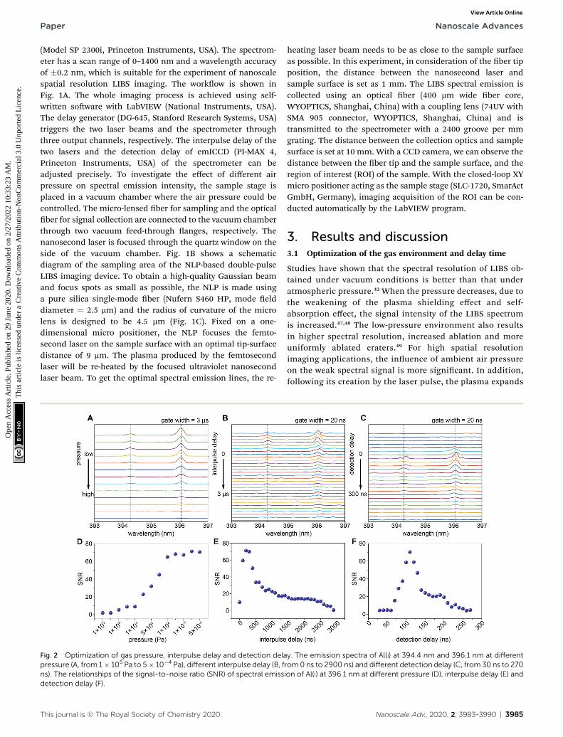
the technology. We rst consider the ALOD and RLOD level ofthis NLP-based nanoscale LIBS imaging method before morecomplicated imaging applications. The ALOD experiment iscarried out on a smooth indium lm. As shown in Fig. 5A, withdifferent laser energy applied to the In lm, different sizes ofcraters can be obtained on the surface of the lm, ranging from
Fig. 5 Evaluation of the ALOD and RLOD. (A) AFM images of ablated craSpectral emission of In(I) at 410.2 nm of the ablated craters of different sizvolume of In. (D) Profile map of the crater on the In film at a laser energy oof In–Sn alloys. (F) Linear fitting of In spectral emission intensity and diff
This journal is © The Royal Society of Chemistry 2020
400 nm to 1.4 mm in diameter. Fig. 5B displays the spectralemissions of In(I) at 410.2 nm for different sizes of craters,which reveals that a positive correlation between signal inten-sity and the crater size (ablated amount) can be established. Thespectra in Fig. 5B represent the average result of three sets ofexperiments. It is worth emphasizing that when the
ters on a smooth In film with different femtosecond laser energies. (B)es in (A). (C) Linear fitting of the spectral emission intensity and ablatedf 61 nJ. (E) Spectral emission of In(I) at 410.2 nm of different proportionserent In concentrations from 1% to 50% in the In–Sn alloy.
Nanoscale Adv., 2020, 2, 3983–3990 | 3987

Fig. 6 Nanoscale LIBS imaging of InP nanoparticles within singe cells.(A and C) Optical image of cells stained with LysoTracker Red DND-99.(B and D) LIBS imaging of In(I) at 410.2 nm.
Nanoscale Advances Paper
Ope
n A
cces
s A
rtic
le. P
ublis
hed
on 2
9 Ju
ne 2
020.
Dow
nloa
ded
on 2
/27/
2022
10:
33:2
3 A
M.
Thi
s ar
ticle
is li
cens
ed u
nder
a C
reat
ive
Com
mon
s A
ttrib
utio
n-N
onC
omm
erci
al 3
.0 U
npor
ted
Lic
ence
.View Article Online
femtosecond laser energy is 47 nJ, the sample crater witha diameter of 400 nm can be clearly observed on the surface ofthe In lm, but its steady emission signal cannot be obtained.Through linear tting, we obtain the relationship between thesignal intensity and different ablated amounts (Fig. 5C). Theerror bars represent the RSDs of the three sets of experimentsand indicate the good stability of the NLP-based double-pulseLIBS technique. The 3-fold standard deviation (3s) value forthe spectral emission intensity in the blank spectrum is 79.3;therefore, the ALOD of NLP-based LIBS for In can be calculatedfrom 3s and the slopes of the calibration curves. Provided thatthe density of In is about 7.31 g cm�3, the resultant ALOD can becalculated to be 18.3 fg. Fig. 5D shows the prole of the craterobtained under the condition of a femtosecond laser energy of61 nJ. It can be seen that the diameter of the crater is about450 nm and the depth is about 100 nm. On the premise of sucha small amount of ablation, we made a linear t through thedetection of the In–Sn alloy with different ratios, and obtainedthe RLOD of In as 0.6% (Fig. 5E and F). It is worth noting thatthe trend of the relationship between LIBS spectral emissionintensity and In concentration might show a slight self-absorption phenomenon in Fig. 5F, which may be caused bythe increase of the number of ground states and excited stateparticles produced by laser interaction with the sample.However, since the vacuum environment can greatly reduce theself-absorption effect, it is not taken into account in the processof linear tting.
3.4 Nanoscale LIBS imaging of single cells
Single cell imaging is an important research direction in theeld of life science.51,52 At present, uorescence imaging is themost commonly used single cell imaging method.23 The appli-cation of LIBS in tissue imaging has been reported with nouorescent probe needed,15 but due to the limitations ofsensitivity and lateral resolution, the application in single cellimaging is still at a blank stage. Due to biocompatibility, beingnon-toxic and other advantages, nanoparticles are widely usedin life science experiments, such as nanoparticle drug loading,nanoparticle photothermal therapy and so on.53–55 Here, weused the NLP-based double-pulse LIBS imaging technology forthe rst time to visually detect the subcellular distribution ofnanoparticles within a single cell. Mouse mononuclear macro-phages leukemia cells and InP nanoparticles are selected forthis research objective. The optical images of the cells anduorescence images of the lysosomes were obtained by usinga confocal laser scanning microscope (CLSM). The cells werethen freeze-dried and placed on the XY micro-positioner in thesampling area. Fig. 6 shows two groups of the comparativeresults of LIBS images of In(I) at 410.2 nm and their opticalimages, with the imaging range of 120 � 90 mm2, respectively.As in the previous experiment, the distance between eachsampling point was set to 500 nm. In the CLSM images, the redchannel represents the position of the lysosomes. As shown inFig. 6B and D, nanoscale LIBS imaging results show that thesignal of In could be detected in cells, and the In distribution isbasically consistent with the location of the lysosomes. Based
3988 | Nanoscale Adv., 2020, 2, 3983–3990
on the result, we can verify the model of cell–nanoparticleinteraction: nanoparticles in aqueous solution enter the cellsthrough endocytosis and reside in the intracellular lysosomes.
4. Conclusions
In conclusion, an NLP-based double-pulse LIBS imaging tech-nology has been proposed with great operability and reliability.With the enhancement of spectral emission using a double-pulse laser and a novel NLP high-resolution samplingapproach, we obtained a signal with a SNR 70� greater thanthat of single-pulse LIBS when the ablated crater size was lessthan 500 nm in diameter on an Al lm. The relative limits ofdetection and absolute limits of detection can reach 0.6% and18.3 fg, respectively, which can be hardly achieved by existingLIBS techniques. Using this method, we visualized the meshsamples and serial numbers on a chip with an imaging reso-lution of 500 nm. Even more exciting, the location of InPnanoparticles in organelles within single cells can also beclearly and quickly obtained, which is helpful in understandingthe interaction between nanomaterials and cells. This strategypresents a nano-scale and sensitive imaging platform forelemental detection, which has great potential in the analysis ofnano materials, microstructures, biological tissues and eventiny biological units such as single cells.
Conflicts of interest
There are no conicts to declare.
Acknowledgements
The authors gratefully acknowledge the nancial support fromthe Natural Science Foundation of China (21974116, 21521004).
This journal is © The Royal Society of Chemistry 2020
Paper Nanoscale Advances
Ope
n A
cces
s A
rtic
le. P
ublis
hed
on 2
9 Ju
ne 2
020.
Dow
nloa
ded
on 2
/27/
2022
10:
33:2
3 A
M.
Thi
s ar
ticle
is li
cens
ed u
nder
a C
reat
ive
Com
mon
s A
ttrib
utio
n-N
onC
omm
erci
al 3
.0 U
npor
ted
Lic
ence
.View Article Online
References
1 D. R. Ifa, N. E. Manicke, A. L. Dill and R. G. Cooks, Science,2008, 321, 805.
2 L. A. McDonnell and R. M. A. Heeren, Mass Spectrom. Rev.,2007, 26, 606–643.
3 X. Hua, H.-W. Li and Y.-T. Long, Anal. Chem., 2018, 90, 1072–1076.
4 J. Han, X. Huang, H. Liu, J. Wang, C. Xiong and Z. Nie, Chem.Sci., 2019, 10, 10958–10962.
5 L. Jolivet, M. Leprince, S. Moncayo, L. Sorbier,C. P. Lienemann and V. Motto-Ros, Spectrochim. Acta, PartB, 2019, 151, 41–53.
6 Q. Lu, Y. Hu, J. Chen and S. Jin, Anal. Chem., 2017, 89, 8238–8243.
7 C. Giesen, H. A. O. Wang, D. Schapiro, N. Zivanovic,A. Jacobs, B. Hattendorf, P. J. Schuffler, D. Grolimund,J. M. Buhmann, S. Brandt, Z. Varga, P. J. Wild, D. Guntherand B. Bodenmiller, Nat. Methods, 2014, 11, 417.
8 X. Li, H. Yin, Z. Wang, Y. Fu, Z. Li and W. Ni, Spectrochim.Acta, Part B, 2015, 111, 102–107.
9 X. Bai, F. Cao, V. Motto-Ros, Q. Ma, Y. Chen and J. Yu,Spectrochim. Acta, Part B, 2015, 113, 158–166.
10 X. Wang, L. Shi, Q. Lin, X. Zhu and Y. Duan, J. Anal. At.Spectrom., 2014, 29, 1098–1104.
11 P. Zheng, H. Liu, J. Wang, B. Yu, B. Zhang, R. Yang andX. Wang, Anal. Methods, 2014, 6, 2163–2169.
12 J. Xiu, S. Zhong, H. Hou, Y. Lu and R. Zheng, Appl. Spectrosc.,2014, 68, 1039–1045.
13 W. Liao, Q. Lin, Y. Xu, E. Yang and Y. Duan, Nanoscale, 2019,11, 5346–5354.
14 D. Dong, L. Jiao, X. Du and C. Zhao, Chem. Commun., 2017,53, 4546–4549.
15 Y. Gimenez, B. Busser, F. Trichard, A. Kulesza, J. M. Laurent,V. Zaun, F. Lux, J. M. Benoit, G. Panczer, P. Dugourd,O. Tillement, F. Pelascini, L. Sancey and V. Motto-Ros, Sci.Rep., 2016, 6, 29936.
16 M. Abdelhamid, F. J. Fortes, M. A. Harith and J. J. Laserna, J.Anal. At. Spectrom., 2011, 26, 1445–1450.
17 M. Bonta, J. J. Gonzalez, C. D. Quarles, R. E. Russo, B. Hegedusand A. Limbeck, J. Anal. At. Spectrom., 2016, 31, 252–258.
18 X. Le Guevel, M. Henry, V. Motto-Ros, E. Longo,M. I. Montanez, F. Pelascini, O. de La Rochefoucauld,P. Zeitoun, J.-L. Coll, V. Josserand and L. Sancey,Nanoscale, 2018, 10, 18657–18664.
19 R. Stockle, P. Setz, V. Deckert, T. Lippert, A. Wokaun andR. Zenobi, Anal. Chem., 2001, 73, 1399–1402.
20 D. Kossakovski and J. L. Beauchamp, Anal. Chem., 2000, 72,4731–4737.
21 V. Zorba, X. Mao and R. E. Russo, Anal. Bioanal. Chem., 2010,396, 173–180.
22 Z. Liang, S. Zhang, X. Li, T. Wang, Y. Huang, W. Hang,Z. Yang, J. Li and Z. Tian, Sci. Adv., 2017, 3, eaaq1059.
23 Z. Yin, X. Cheng, R. Liu, X. Li, L. Hang, W. Hang, J. Xu,X. Yan, J. Li and Z. Tian, Angew. Chem., Int. Ed., 2019, 58,4541–4546.
This journal is © The Royal Society of Chemistry 2020
24 D. Menut, P. Fichet, J.-L. Lacour, A. Rivoallan andP. Mauchien, Appl. Opt., 2003, 42, 6063–6071.
25 X. Wang, V. Motto-Ros, G. Panczer, D. De Ligny, J. Yu,J. M. Benoit, J. L. Dussossoy and S. Peuget, Spectrochim.Acta, Part B, 2013, 87, 139–146.
26 M. S. Afgan, Z. Hou and Z. Wang, J. Anal. At. Spectrom., 2017,32, 1905–1915.
27 D. Bauerle, Laser Processing and Chemistry, Springer Science& Business Media, 2013.
28 P. P. Pronko, S. K. Dutta, D. Du and R. K. Singh, J. Appl. Phys.,1995, 78, 6233–6240.
29 H. Hou, L. Cheng, T. Richardson, G. Chen, M. Doeff,R. Zheng, R. Russo and V. Zorba, J. Anal. At. Spectrom.,2015, 30, 2295–2302.
30 M.Wang, L. Jiang, S. Wang, Q. Guo, F. Tian, Z. Chu, J. Zhang,X. Li and Y. Lu, Anal. Chem., 2019, 91, 9952–9961.
31 P. P. Pronko, S. K. Dutta, J. Squier, J. V. Rudd, D. Du andG. Mourou, Opt. Commun., 1995, 114, 106–110.
32 Y. Cui, I. V. Veryovkin, M. W. Majeski, D. R. Cavazos andL. Hanley, Anal. Chem., 2015, 87, 367–371.
33 L. Novotny and S. J. Stranick, Annu. Rev. Phys. Chem., 2006,57, 303–331.
34 Z. Liang, Z. Yin, H. Yang, Y. Xiao, W. Hang and J. Li, TrAC,Trends Anal. Chem., 2016, 75, 24–34.
35 N. Abeyasinghe, S. Kumar, K. Sun, J. F. Manseld, R. Jin andT. Goodson, J. Am. Chem. Soc., 2016, 138, 16299–16307.
36 D. Cleveland and R. G. Michel, Appl. Spectrosc. Rev., 2008, 43,93–110.
37 O. Samek, A. Kurowski, S. Kittel, S. Kukhlevsky andR. Hergenroder, Spectrochim. Acta, Part B, 2005, 60, 1225–1229.
38 D. J. Hwang, C. P. Grigoropoulos, J. Yoo and R. E. Russo,Appl. Phys. Lett., 2006, 89, 254101.
39 D. J. Hwang, H. Jeon, C. P. Grigoropoulos, J. Yoo andR. E. Russo, J. Appl. Phys., 2008, 104, 013110.
40 M. V. Zoriy, M. Kayser and J. S. Becker, Int. J. Mass Spectrom.,2008, 273, 151–155.
41 J. S. Becker, A. Gorbunoff, M. Zoriy, A. Izmer and M. Kayser,J. Anal. At. Spectrom., 2006, 21, 19–25.
42 X. Wang, Z. Liang, Y. Meng, T. Wang, W. Hang andB. Huang, Spectrochim. Acta, Part B, 2018, 141, 1–6.
43 J. Scaffidi, S. M. Angel and D. A. Cremers, Anal. Chem., 2006,78, 24–32.
44 D. A. Cremers, L. J. Radziemski and T. R. Loree, Appl.Spectrosc., 1984, 38, 721–729.
45 J. Uebbing, J. Brust, W. Sdorra, F. Leis and K. Niemax, Appl.Spectrosc., 1991, 45, 1419–1423.
46 Y. Lu, V. Zorba, X. Mao, R. Zheng and R. E. Russo, J. Anal. At.Spectrom., 2013, 28, 743–748.
47 G. Cristoforetti, Spectrochim. Acta, Part B, 2009, 64, 26–34.48 G. Cristoforetti, S. Legnaioli, V. Palleschi, A. Salvetti and
E. Tognoni, Spectrochim. Acta, Part B, 2004, 59, 1907–1917.
49 A. J. Effenberger Jr and J. R. Scott, Sensors, 2010, 10, 4907–4925.
50 K. Rifai, S. Laville, F. Vidal, M. Sabsabi and M. Chaker, J.Anal. At. Spectrom., 2012, 27, 276–283.
Nanoscale Adv., 2020, 2, 3983–3990 | 3989

Nanoscale Advances Paper
Ope
n A
cces
s A
rtic
le. P
ublis
hed
on 2
9 Ju
ne 2
020.
Dow
nloa
ded
on 2
/27/
2022
10:
33:2
3 A
M.
Thi
s ar
ticle
is li
cens
ed u
nder
a C
reat
ive
Com
mon
s A
ttrib
utio
n-N
onC
omm
erci
al 3
.0 U
npor
ted
Lic
ence
.View Article Online
51 R. Zenobi, Science, 2013, 342, 1243259.52 J. Pisonero, D. Bouzas-Ramos, H. Traub, B. Cappella,
C. Alvarez-Llamas, S. Richter, J. C. Mayo, J. M. Costa-Fernandez, N. Bordel and N. Jakubowski, J. Anal. At.Spectrom., 2019, 34, 655–663.
3990 | Nanoscale Adv., 2020, 2, 3983–3990
53 E. Hinde, K. Thammasiraphop, H. T. T. Duong, J. Yeow,B. Karagoz, C. Boyer, J. J. Gooding and K. Gaus, Nat.Nanotechnol., 2016, 12, 81.
54 X. Ma, Y. Wu, S. Jin, Y. Tian, X. Zhang, Y. Zhao, L. Yu andX.-J. Liang, ACS Nano, 2011, 5, 8629–8639.
55 Z. Zhao, D. Huang, Z. Yin, X. Chi, X. Wang and J. Gao, J.Mater. Chem., 2012, 22, 15717–15725.
This journal is © The Royal Society of Chemistry 2020