Embed Size (px)
Citation preview

Characterization of opticalcoatings by photothermal deflection
Mireille Commandre and Pierre Roche
An overview of photothermal deflection principles and applications is given. The modeling of temper-ature distribution and the calculation of deflection that is due to both the refractive-index gradient andthe thermal deformation of the sample are presented. Three configurations usually employed arecompared, and their respective advantages are discussed in relation to their application. The calibrationfor absolute measurement of absorption is detailed, showing that calibration limits the accuracy ofmeasurement. Some examples of specific information obtained by photothermal mapping of absorptionare given. © 1996 Optical Society of America
Key words: Optical coatings, photothermal deflection, calibration, absorption, local defects.
1. Introduction
Optical absorption is responsible for decreases of re-flectance and transmittance values for dielectric thin-film optical components and then acts as a limitingfactor for optical performances but also causes re-duced values of the radiation damage threshold.1–3Indeed, absorbed radiative energy is converted toheat that propagates through the sample, and theinduced temperature change can lead to damage.Radiation damage resistance has been shown to bedependent on both absorption losses and thermo-physical properties of materials, especially thethermal conductivity.4–6 Furthermore, substantialprogress has been made in thin-film technology dur-ing past few years, and classical values of losses arenow in the 1026–1024 range. However, the determi-nation of losses by measurement of reflectance ~R!and transmittance ~T! is limited to 1 2 R 2 T . 1023.Under these conditions, an accurate characterizationof absorption and thermal properties of optical thinfilms has become an important task for the improve-ment of optical performances and a better under-standing of damage mechanisms.
The authors are with the Laboratoire d’Optique des Surfaces etdes Couches Minces, Unite Associee au Centre National de laRecherche Scientifique, Ecole Nationale Superieure de Physiquede Marseille, Domaine Universitaire de St. Jerome, 13397 Mar-seille Cedex 20, France.Received 20 November 1995; revised manuscript received 4
March 1996.0003-6935y96y255021-14$10.00y0© 1996 Optical Society of America
Photothermal deflection ~PD! techniques were de-veloped at the beginning of the 1980’s7–9 and havebeen widely employed since to characterize opticalcoatings.3,10–25 The basic process of photothermalmethods is measuring the heating of the samplecaused by optical absorption. In PD, the heated do-main is probed by a laser beam that is deflected.Because of the order of magnitude of thermal effects,all the photothermal methods require a time-dependent excitation light. Each technique can beused in both modulated or pulsed modes. Resultingfrom the optical absorption of the intensity-modulated ~or pulsed! pump beam, a local tempera-ture rise occurs and a thermal wave propagates in thestructure. This modulated ~or pulsed! temperaturerise is accompanied by spatial refractive-index vari-ations and a buckling of the sample surface that isdue to thermal expansion. PD lies in measuring thedeflection of the probe beam, which is due to therefractive-index gradients and to the thermal buck-ling of the sample surface. Obviously amplitude andphase of the PD signal depend on both the opticalabsorption and thermal properties of the thin film.At a low modulation frequency, one can obtain theabsorptance value on the conditions that a propercalibration has been performed and frequency or tem-poral response can give information about thermalproperties ~diffusivity or thermal conductivity!.Furthermore, PD is a direct measurement of ab-
sorbed energy; thereby the photothermal signal islinear over a large range of absorbed optical powerand is vanishing when there is no absorption. PD isalso insensitive to scattered light, at least the exter-nal part. The success of PD originates from various
1 September 1996 y Vol. 35, No. 25 y APPLIED OPTICS 5021
5
Fig. 1. Different experimental configurations for PD measurement: ~a! classi-cal mirage effect configuration in which the probe beam is parallel to the samplesurface; ~b! transmission configuration in which the deflection of the transmittedprobe beam is measured; ~c! reflection configuration in which the deflection of thereflected beam is measured.
other advantages: the absence of any mechanicalcontact with the sample ~PD is a nondestructivemethod! and the ease of implementing ~no samplepreparation, for example!. For absorption measure-ment, the greatest advantages are high sensitivityand the possible application to spectroscopy andabove all to high spatial resolution imaging.In this paper we present an overview of three con-
figurations ~defined by the relative positions of theprobe beam and the sample! that have been used forimplementing this technique and their applications.This overview does not give complete insight into thegreat variety of the photothermal methods that canbe used, but we have selected these three schemesbecause they can be carried out with exactly the sameexperimental setup and they are complementary.We present a short survey of the modeling of temper-ature distribution and the calculation of PD that isdue to the refractive-index gradient as well as to thethermal buckling of the sample. The orders of mag-nitude of these two components are compared in thedifferent configurations. We take a special interestin showing the advantages of each configuration, de-pending on the application.PD permits accurate measurements of very small
absorption losses as low as 1026. We describe anexperimental setup realized in our laboratory forabsorption mapping. Calibration is an importanttask that is detailed. Absorption mapping hasbeen shown to be a complementary tool for the char-acterization of the cleanness and optical quality of
022 APPLIED OPTICS y Vol. 35, No. 25 y 1 September 1996
bare substrates,18–20 and some results are pre-sented.
2. Photothermal Deflection Principles and Applications
In Fig. 1 we present three schemes that have beenused for implementing this technique. Figure 1~a! isthe classical mirage effect or transverse configura-tion: The probe beam is in the air, parallel to thesample surface and is deflected by the index gradientin air in the direction normal to the surface. Belowwe call the scheme given in Fig. 1~b! the transmissionconfiguration ~also called the collinear configuration!:The probe beam goes through the sample and is de-flected by both the radial index gradient in the threemedia and the surface displacement. We refer tothe scheme given in Fig. 1~c! as the reflection config-uration: The deflection of the reflected probe beamis measured and originates from the index gradientin the air and in the coating and from the thermalexpansion of the surface.Some variants can be used: For example, in the
reflection configuration, the probe beam can be di-rected to the sample back surface and propagate inthe substrate. Or in the mirage effect, the probebeam can go through the sample under the surface~polished lateral faces are then required for the sub-strate!.
A. Modeling of Photothermal Deflection
The calculation of PD can be divided into two parts.First, by using the expression of heat source resulting
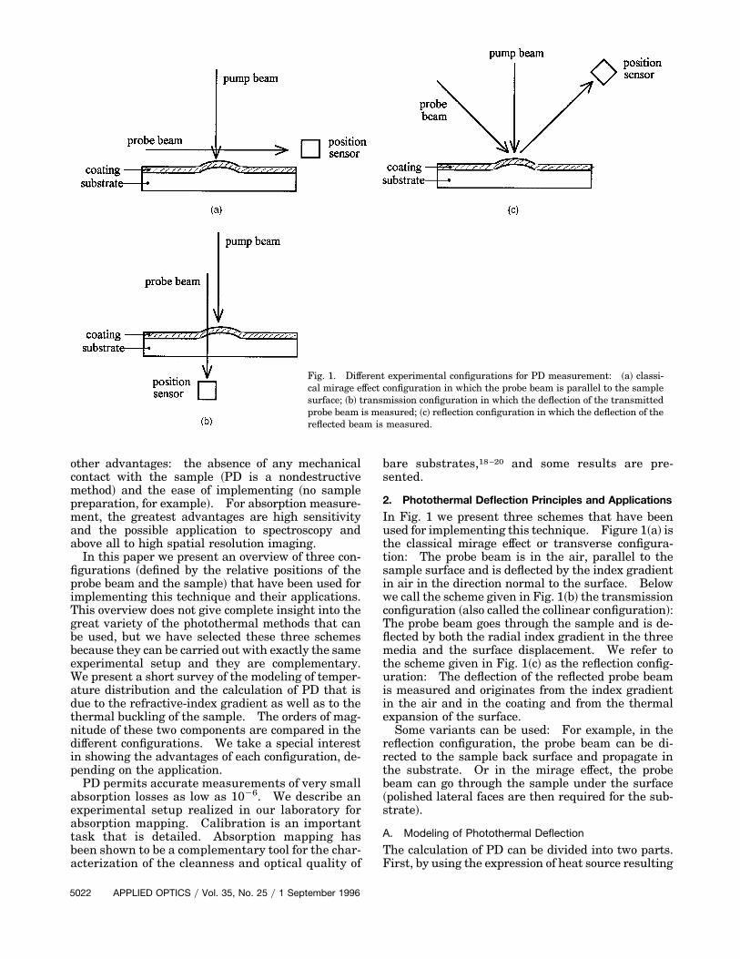
from optical absorption in the coating, we calculatethe modulated temperature distribution in the threemedia, air, coating, and substrate. Then the effectsof temperature distribution on the probe-beam prop-agation can be calculated. The notation of differentparameters is given in Fig. 2. The air and the sub-strate are assumed to be transparent and semi-infinite. The film is infinite in both the x and the ydirections. The pump beam is normal to the samplesurface and is assumed to be Gaussian.
1. Calculation of Modulated TemperatureWe denote as Ti~x, y, z, t! the time-dependent com-ponent of temperature distribution in medium i.The calculation of the steady temperature rise can befound in Ref. 26. The three media are assumed to beisotropic, so the temperature distribution keeps a cy-lindrical symmetryTi~r, z, t!where r
2 5 x2 1 y2, as forthe pump beam. In this paper we are interested inonly harmonic solutions: Ti~r, z, t! 5 Ti~r, z!exp~ jvt!. The equations governing the thermal phe-nomena are considered with the assumption thatheat transfer is due only to thermal conduction: Ra-diation losses and natural convection are negligibleat ambient temperature.27 Furthermore, tempera-ture distribution is assumed to be unaffected by thethermal buckling of the sample.8,9Under these conditions, temperature distribution
in the three media satisfies the equations of heatdiffusion8:
¹2T0~r, z, t! 2r0C0
K0
]T0
]t5 0, (1)
¹2T1~r, z, t! 2r1C1
K1
]T1
]t5
2Q1~r, z, t!K1
, (2)
¹2T2~r, z, t! 2r2C2
K2
]T2
]t5 0, (3)
Fig. 2. Definition of notation used in the text: ni and ki are thereal and the imaginary parts of the complex index of medium i,respectively ~i 5 0 to 2!, Ki is the thermal conductivity of mediumi, ri is themass density of medium i,Ci is the heat capacity per unitmass of medium i, n is the modulation frequency, v 5 2pn is themodulation pulsation of the pump beam, mi is the thermal diffusionlength of medium i defined by mi 5 ~KiyriCipn!1y2, RFA and RFS arethe thermal resistances at the air–film and film–substrate inter-faces, respectively, e is the film thickness, and 2a is the diameterat 1ye2 of the Gaussian pump beam.
with the following conditions at the boundaries z 5 0and z 5 e:
T0~z 5 0! 5 T1~z 5 0! 2 RFAFF3A, (4)
T1~z 5 e! 5 T2~z 5 e! 1 RFSFF3S, (5)
FF3S 5 2K1S]T1
]z Dz5e
5 2K2S]T2
]z Dz5e
, (6)
FF3A 5 K0S]T0
]z Dz50
5 K1S]T1
]z Dz50
. (7)
Relations ~4! and ~5! are the equations of continuityfor the temperature ~taking into account the thermalresistance at the interfaces!, and relations ~6! and ~7!are the equations of continuity for the heat flows.Q1~r, z, t! is the heat source resulting from the
optical absorption in the film, and FF3A and FF3Sare the heat flows from the film toward the air andthe substrate.If we take into account the interference effects in
the film, the expression of the heat term is
Q1~r, z, t! 54pk1
l
n1n0
P0
pa2exp~22r2ya2!
3 exp~ jvt!UE1~z!E0
U2 , (8)
where P0 is the incident power of the pump beam, ais the 1ye2 radius of the pump beam, and Ei is theelectric field in the medium i ~i 5 0, 1!. uE1yE0u
2 is asinusoidal function of z, with a period of ly2.We can note that, in the low modulation frequency
range, the thermal diffusion length @defined by mi 5~KiyriCipn!1y2# of the film is higher than its thickness~e , m1, thermally thin film!. In this case the vari-ation of the heat source with z can be ignored, and amean-energy approximation is valuable for calculat-ing the temperature distribution in the three media.These equations can be solved with the radial Fou-
rier transform:
Ti~r, z! 5 2p *0
`
sJ0~2psr!Ti~s, z!ds, ~i 5 0 to 2!,
(9)
where J0 is the Bessel function of the order of 0.Some general statements can be made about the
form of the solutions. The temperature rise in thethree media is always proportional to the incidentpower of the pump beam P0 and to the extinctioncoefficient k1 of the film. The thermal conductivityof the film K1 appears at different places in expres-sions of temperature rises; this parameter plays animportant part in the temperature distribution.To gain physical insight into thermal wave propa-
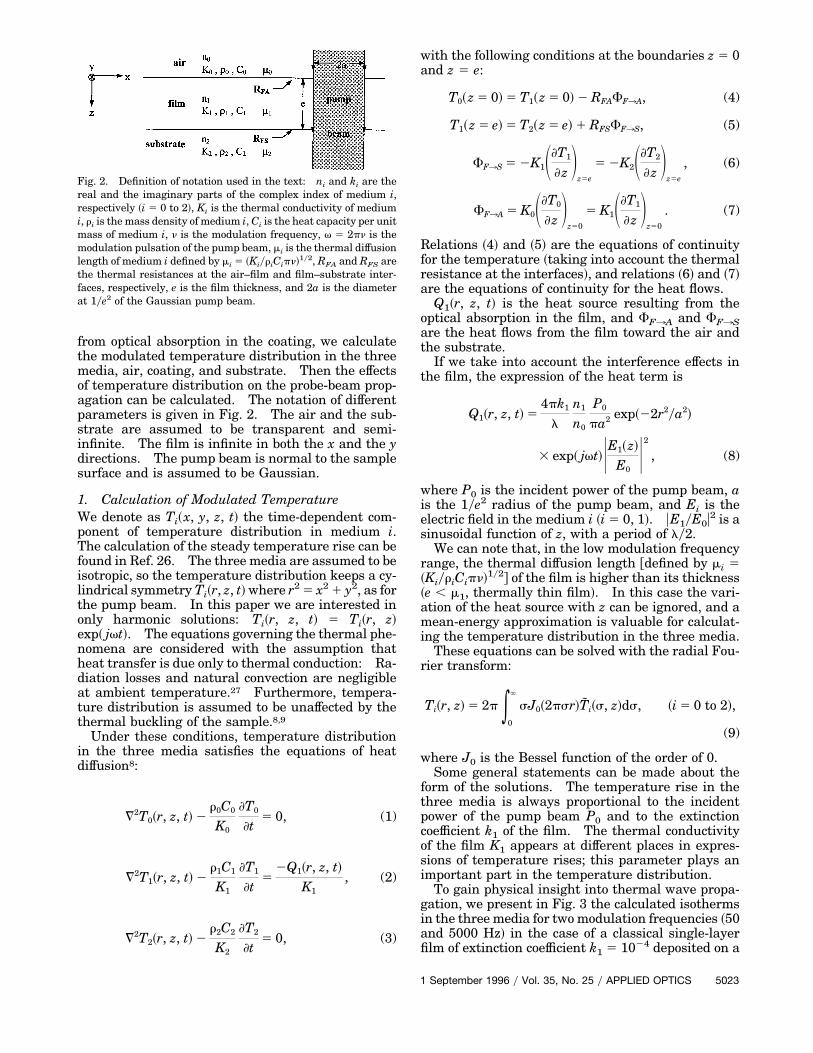
gation, we present in Fig. 3 the calculated isothermsin the threemedia for twomodulation frequencies ~50and 5000 Hz! in the case of a classical single-layerfilm of extinction coefficient k1 5 1024 deposited on a
1 September 1996 y Vol. 35, No. 25 y APPLIED OPTICS 5023
fused-silica substrate. The value of the thermal dif-fusion length is given in each case for substrate andair. Physically the thermal diffusion length is thedistance over which the amplitude of a planar har-monic thermal wave decays exponentially to 1ye of itsinitial value. For low modulation frequency ~Fig.3a! the thermal diffusion length in the two media islarger than the radius at 1ye2 of the pump beam:The temperature rise ~the values are given for theisotherms in degrees Celsius! extends in the x, yplane beyond the pump-beam profile. For highmod-ulation frequency ~Fig. 3b! the thermal diffusionlength decreases: The heated domain is reducedand nearly coincides with the illuminated domain inthe radial direction.The different refractive-index gradients that are
probed in the different configurations of PD can beeasily seen. The radial gradient associated with theenergetic profile of the pump beam is probed in thetransmission configuration, whereas the gradient inthe direction perpendicular to the sample surface isprobed in the transverse one.
2. Photothermal Deflection that is due to theRefractive-Index GradientWe neglect the effect of the acoustic wave that accom-panies the temperature rise. The measured deflec-tions are generally very small, lower than 1025 rad;the total shift of the probe beam is lower than 0.1 mm,which is small compared with the probe-beam diam-eter ~'40 mm!. Under these conditions, if the probebeam propagates in the Z direction, the deflection in
Fig. 3. Modulated temperature distribution in the three media:isotherms calculated with classical values of thermal parametersfor the film ~e 5 0.5 mm, k1 5 1024, K1 5 0.1 WymK, fused-silicasubstrate, P0 5 1 W, a 5 25 mm!: ~a! n 5 50 Hz, ~b! n 5 5000 Hz.
5024 APPLIED OPTICS y Vol. 35, No. 25 y 1 September 1996
the Y direction is given8 for the medium i by
uY,i 51ni
]ni]T *
path i
dZF]Ti
]Y~X, Y, Z, t!G
X5X0,Y5Y0
, (10)
where ~X0, Y0! is the position of the probe-beam cen-ter in the plane Z 5 0 and ]niy]T is the temperaturecoefficient of the refractive index of medium i.The PD is always linearly related to the incident
power of the pump beam and to the extinction coef-ficient of the film.In Refs. 8, 18, and 25 one can find some examples
of the calculation of deflection versus relative posi-tions of pump- and probe-beam centers for transmis-sion configuration and versus distance betweensample surface and probe-beam center for a mirageeffect.For the transmission configuration, the total de-
flection is the sum of complex deflections in the threemedia: air, film, and substrate. The deflection inthe substrate is generally predominant.18 The de-flection inside the film is proportional to 1yn1 ]n1y]T,and it is generally small for thin films ~e # 1 mm!.But we can remark that, concerning values of 1yn1]n1y]T, only some data can be found in publica-tions,28 and the sign and the absolute value of thisparameter are different from the bulk ones. Thesign plays an important role because it changes thephase of the deflection in the film.
3. Calculation of Deflection that is due to ThermalDisplacementFor the transmission and the reflection configura-tions, there are two contributions to PD: index gra-dients and thermal expansion of the surfaces. Thecalculation of the deflection that is due to the ther-moelastic deformation of the sample surface has beendeveloped in Refs. 9 and 29. The rigorous calcula-tion involves solving the Navier–Stokes equations:
~1 2 2ni!¹2u 1 ¹~¹ z u! 5 2~1 1 ni!ai¹T ~i 5 1, 2!,
where u is the displacement vector, ni is the Poissonratio, and ai is the thermal expansion coefficient ofmedium i. Only approximate analytic solutions areavailable. If the probe beam propagates in the Zdirection, the deflection in the Y direction is given by
uY < 2]uz]Y
~X0, Y0, Z 5 0! 1 2]uz]Y
~X0, Y0, Z 5 e!
for the reflection configuration and by
uY < ~n1 2 n0!]uz]Y
~X0, Y0, Z 5 0!
1 ~n2 2 n1!]uz]Y
~X0, Y0, Z 5 e!
for the transmission configuration, where ~X0, Y0! isthe position of the probe-beam center in the plane Z50. The first term in these equations corresponds tothe deflection at the air–film interface and the second
one to the deflection at the film–substrate interface.The thermal deformations of the film and the sub-strate contribute together to the total deflection.One shows that each deflection is proportional to theconsidered thermal expansion coefficient.Comparative calculations of the two contributions,
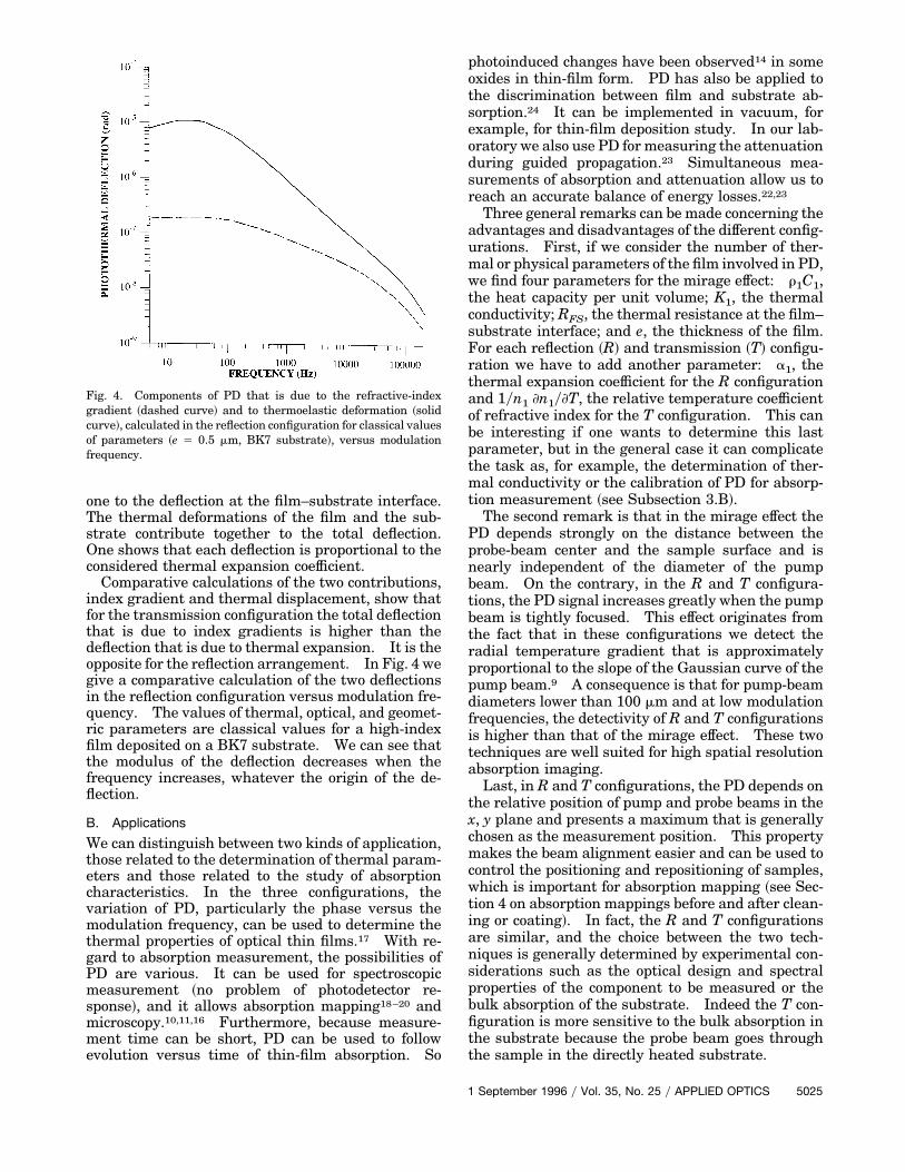
index gradient and thermal displacement, show thatfor the transmission configuration the total deflectionthat is due to index gradients is higher than thedeflection that is due to thermal expansion. It is theopposite for the reflection arrangement. In Fig. 4 wegive a comparative calculation of the two deflectionsin the reflection configuration versus modulation fre-quency. The values of thermal, optical, and geomet-ric parameters are classical values for a high-indexfilm deposited on a BK7 substrate. We can see thatthe modulus of the deflection decreases when thefrequency increases, whatever the origin of the de-flection.
B. Applications
We can distinguish between two kinds of application,those related to the determination of thermal param-eters and those related to the study of absorptioncharacteristics. In the three configurations, thevariation of PD, particularly the phase versus themodulation frequency, can be used to determine thethermal properties of optical thin films.17 With re-gard to absorption measurement, the possibilities ofPD are various. It can be used for spectroscopicmeasurement ~no problem of photodetector re-sponse!, and it allows absorption mapping18–20 andmicroscopy.10,11,16 Furthermore, because measure-ment time can be short, PD can be used to followevolution versus time of thin-film absorption. So
Fig. 4. Components of PD that is due to the refractive-indexgradient ~dashed curve! and to thermoelastic deformation ~solidcurve!, calculated in the reflection configuration for classical valuesof parameters ~e 5 0.5 mm, BK7 substrate!, versus modulationfrequency.
photoinduced changes have been observed14 in someoxides in thin-film form. PD has also be applied tothe discrimination between film and substrate ab-sorption.24 It can be implemented in vacuum, forexample, for thin-film deposition study. In our lab-oratory we also use PD for measuring the attenuationduring guided propagation.23 Simultaneous mea-surements of absorption and attenuation allow us toreach an accurate balance of energy losses.22,23Three general remarks can bemade concerning the
advantages and disadvantages of the different config-urations. First, if we consider the number of ther-mal or physical parameters of the film involved in PD,we find four parameters for the mirage effect: r1C1,the heat capacity per unit volume; K1, the thermalconductivity; RFS, the thermal resistance at the film–substrate interface; and e, the thickness of the film.For each reflection ~R! and transmission ~T! configu-ration we have to add another parameter: a1, thethermal expansion coefficient for the R configurationand 1yn1 ]n1y]T, the relative temperature coefficientof refractive index for the T configuration. This canbe interesting if one wants to determine this lastparameter, but in the general case it can complicatethe task as, for example, the determination of ther-mal conductivity or the calibration of PD for absorp-tion measurement ~see Subsection 3.B!.The second remark is that in the mirage effect the
PD depends strongly on the distance between theprobe-beam center and the sample surface and isnearly independent of the diameter of the pumpbeam. On the contrary, in the R and T configura-tions, the PD signal increases greatly when the pumpbeam is tightly focused. This effect originates fromthe fact that in these configurations we detect theradial temperature gradient that is approximatelyproportional to the slope of the Gaussian curve of thepump beam.9 A consequence is that for pump-beamdiameters lower than 100 mm and at low modulationfrequencies, the detectivity of R and T configurationsis higher than that of the mirage effect. These twotechniques are well suited for high spatial resolutionabsorption imaging.Last, in R and T configurations, the PD depends on
the relative position of pump and probe beams in thex, y plane and presents a maximum that is generallychosen as the measurement position. This propertymakes the beam alignment easier and can be used tocontrol the positioning and repositioning of samples,which is important for absorption mapping ~see Sec-tion 4 on absorption mappings before and after clean-ing or coating!. In fact, the R and T configurationsare similar, and the choice between the two tech-niques is generally determined by experimental con-siderations such as the optical design and spectralproperties of the component to be measured or thebulk absorption of the substrate. Indeed the T con-figuration is more sensitive to the bulk absorption inthe substrate because the probe beam goes throughthe sample in the directly heated substrate.
1 September 1996 y Vol. 35, No. 25 y APPLIED OPTICS 5025
3. Experimental Procedure for Absorption Mapping
A. Experimental Setup
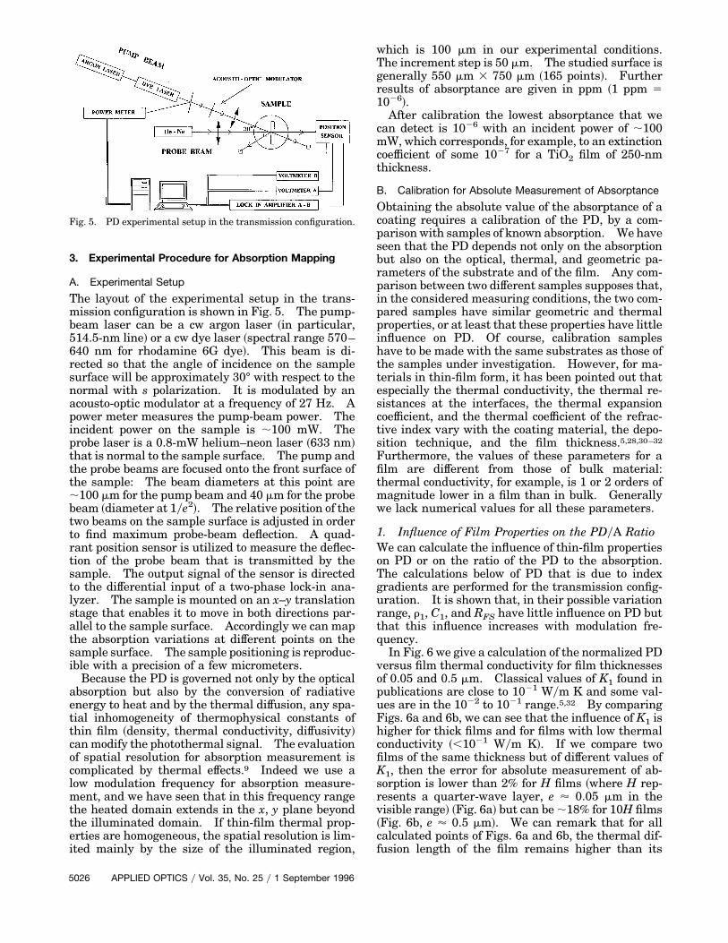
The layout of the experimental setup in the trans-mission configuration is shown in Fig. 5. The pump-beam laser can be a cw argon laser ~in particular,514.5-nm line! or a cw dye laser ~spectral range 570–640 nm for rhodamine 6G dye!. This beam is di-rected so that the angle of incidence on the samplesurface will be approximately 30° with respect to thenormal with s polarization. It is modulated by anacousto-optic modulator at a frequency of 27 Hz. Apower meter measures the pump-beam power. Theincident power on the sample is ;100 mW. Theprobe laser is a 0.8-mW helium–neon laser ~633 nm!that is normal to the sample surface. The pump andthe probe beams are focused onto the front surface ofthe sample: The beam diameters at this point are;100 mm for the pump beam and 40 mm for the probebeam ~diameter at 1ye2!. The relative position of thetwo beams on the sample surface is adjusted in orderto find maximum probe-beam deflection. A quad-rant position sensor is utilized to measure the deflec-tion of the probe beam that is transmitted by thesample. The output signal of the sensor is directedto the differential input of a two-phase lock-in ana-lyzer. The sample is mounted on an x–y translationstage that enables it to move in both directions par-allel to the sample surface. Accordingly we can mapthe absorption variations at different points on thesample surface. The sample positioning is reproduc-ible with a precision of a few micrometers.Because the PD is governed not only by the optical
absorption but also by the conversion of radiativeenergy to heat and by the thermal diffusion, any spa-tial inhomogeneity of thermophysical constants ofthin film ~density, thermal conductivity, diffusivity!canmodify the photothermal signal. The evaluationof spatial resolution for absorption measurement iscomplicated by thermal effects.9 Indeed we use alow modulation frequency for absorption measure-ment, and we have seen that in this frequency rangethe heated domain extends in the x, y plane beyondthe illuminated domain. If thin-film thermal prop-erties are homogeneous, the spatial resolution is lim-ited mainly by the size of the illuminated region,
Fig. 5. PD experimental setup in the transmission configuration.
5026 APPLIED OPTICS y Vol. 35, No. 25 y 1 September 1996
which is 100 mm in our experimental conditions.The increment step is 50 mm. The studied surface isgenerally 550 mm 3 750 mm ~165 points!. Furtherresults of absorptance are given in ppm ~1 ppm 51026!.After calibration the lowest absorptance that we
can detect is 1026 with an incident power of ;100mW, which corresponds, for example, to an extinctioncoefficient of some 1027 for a TiO2 film of 250-nmthickness.
B. Calibration for Absolute Measurement of Absorptance
Obtaining the absolute value of the absorptance of acoating requires a calibration of the PD, by a com-parisonwith samples of known absorption. We haveseen that the PD depends not only on the absorptionbut also on the optical, thermal, and geometric pa-rameters of the substrate and of the film. Any com-parison between two different samples supposes that,in the considered measuring conditions, the two com-pared samples have similar geometric and thermalproperties, or at least that these properties have littleinfluence on PD. Of course, calibration sampleshave to be made with the same substrates as those ofthe samples under investigation. However, for ma-terials in thin-film form, it has been pointed out thatespecially the thermal conductivity, the thermal re-sistances at the interfaces, the thermal expansioncoefficient, and the thermal coefficient of the refrac-tive index vary with the coating material, the depo-sition technique, and the film thickness.5,28,30–32Furthermore, the values of these parameters for afilm are different from those of bulk material:thermal conductivity, for example, is 1 or 2 orders ofmagnitude lower in a film than in bulk. Generallywe lack numerical values for all these parameters.
1. Influence of Film Properties on the PDyA RatioWe can calculate the influence of thin-film propertieson PD or on the ratio of the PD to the absorption.The calculations below of PD that is due to indexgradients are performed for the transmission config-uration. It is shown that, in their possible variationrange, r1, C1, and RFS have little influence on PD butthat this influence increases with modulation fre-quency.In Fig. 6 we give a calculation of the normalized PD
versus film thermal conductivity for film thicknessesof 0.05 and 0.5 mm. Classical values of K1 found inpublications are close to 1021 Wym K and some val-ues are in the 1022 to 1021 range.5,32 By comparingFigs. 6a and 6b, we can see that the influence of K1 ishigher for thick films and for films with low thermalconductivity ~,1021 Wym K!. If we compare twofilms of the same thickness but of different values ofK1, then the error for absolute measurement of ab-sorption is lower than 2% for H films ~where H rep-resents a quarter-wave layer, e ' 0.05 mm in thevisible range! ~Fig. 6a! but can be;18% for 10H films~Fig. 6b, e ' 0.5 mm!. We can remark that for allcalculated points of Figs. 6a and 6b, the thermal dif-fusion length of the film remains higher than its
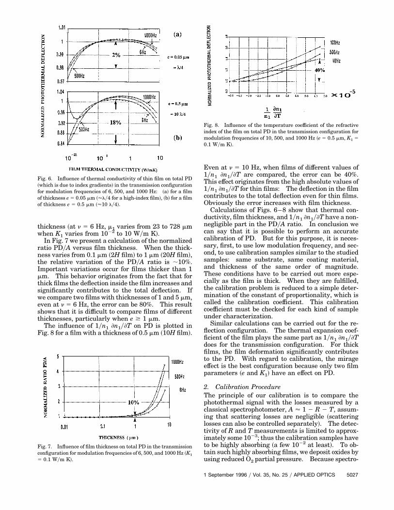
thickness ~at n 5 6 Hz, m1 varies from 23 to 728 mmwhen K1 varies from 1022 to 10 Wym K!.In Fig. 7 we present a calculation of the normalized
ratio PDyA versus film thickness. When the thick-ness varies from 0.1 mm ~2H film! to 1 mm ~20H film!,the relative variation of the PDyA ratio is ;10%.Important variations occur for films thicker than 1mm. This behavior originates from the fact that forthick films the deflection inside the film increases andsignificantly contributes to the total deflection. Ifwe compare two films with thicknesses of 1 and 5 mm,even at n 5 6 Hz, the error can be 80%. This resultshows that it is difficult to compare films of differentthicknesses, particularly when e $ 1 mm.The influence of 1yn1 ]n1y]T on PD is plotted in
Fig. 8 for a film with a thickness of 0.5 mm ~10H film!.
Fig. 6. Influence of thermal conductivity of thin film on total PD~which is due to index gradients! in the transmission configurationfor modulation frequencies of 6, 500, and 1000 Hz: ~a! for a filmof thickness e 5 0.05 mm ~'ly4 for a high-index film!, ~b! for a filmof thickness e 5 0.5 mm ~'10 ly4!.
Fig. 7. Influence of film thickness on total PD in the transmissionconfiguration for modulation frequencies of 6, 500, and 1000Hz ~K1
5 0.1 Wym K!.
Even at n 5 10 Hz, when films of different values of1yn1 ]n1y]T are compared, the error can be 40%.This effect originates from the high absolute values of1yn1 ]n1y]T for thin films: The deflection in the filmcontributes to the total deflection even for thin films.Obviously the error increases with film thickness.Calculations of Figs. 6–8 show that thermal con-
ductivity, film thickness, and 1yn1 ]n1y]T have a non-negligible part in the PDyA ratio. In conclusion wecan say that it is possible to perform an accuratecalibration of PD. But for this purpose, it is neces-sary, first, to use low modulation frequency, and sec-ond, to use calibration samples similar to the studiedsamples: same substrate, same coating material,and thickness of the same order of magnitude.These conditions have to be carried out more espe-cially as the film is thick. When they are fulfilled,the calibration problem is reduced to a simple deter-mination of the constant of proportionality, which iscalled the calibration coefficient. This calibrationcoefficient must be checked for each kind of sampleunder characterization.Similar calculations can be carried out for the re-
flection configuration. The thermal expansion coef-ficient of the film plays the same part as 1yn1 ]n1y]Tdoes for the transmission configuration. For thickfilms, the film deformation significantly contributesto the PD. With regard to calibration, the mirageeffect is the best configuration because only two filmparameters ~e and K1! have an effect on PD.
2. Calibration ProcedureThe principle of our calibration is to compare thephotothermal signal with the losses measured by aclassical spectrophotometer, A ' 1 2 R 2 T, assum-ing that scattering losses are negligible ~scatteringlosses can also be controlled separately!. The detec-tivity of R and T measurements is limited to approx-imately some 1023; thus the calibration samples haveto be highly absorbing ~a few 1022 at least!. To ob-tain such highly absorbing films, we deposit oxides byusing reduced O2 partial pressure. Because spectro-
Fig. 8. Influence of the temperature coefficient of the refractiveindex of the film on total PD in the transmission configuration formodulation frequencies of 10, 500, and 1000 Hz ~e 5 0.5 mm, K1 50.1 Wym K!.
1 September 1996 y Vol. 35, No. 25 y APPLIED OPTICS 5027

Table 1. Comparison among Absorptances Measured by PD and by33 LM for Four SiO2 Films of Increasing Thicknesses
OpticalThickness
Absorptance ~31024!Measured by PDa
Absorptance ~31024!Measured by LMb
Ratio
Simple RatioCorrected Ratio
3 l2yl1 1ycos ifilm
l2y4 1.0 6 0.2 1.4 1.40 1.28s 5 1.1
l2y2 2.1 6 0.4 3 1.43 1.30'1.3s 5 0.23
3l2y4 2.2 6 0.4 3 1.36 1.24s 5 0.6
l2 3.4 6 0.7 5 1.47 1.34s 5 0.2
Bare substrate~fused silica!
0.28 6 0.06s 5 0.2
al1 5 600 nm, iair 5 30°, s polarization.bl2 5 514.5 nm, normal incidence.
photometric and photothermal measurements have adifferent spatial resolution, we compare the meanvalues of absorptance on the same 3 mm 3 3 mmarea.The accuracy of absolute measurement of absorp-
tion by PD is limited by the calibration. When var-ious calibration samples with similar characteristicsare used, the dispersion of measured calibration co-efficients is ;20% when the relative uncertainty ofthe photothermal signal is some percent only.18
3. Comparison among Measurements by LaserMicrocalorimetry and Photothermal DeflectionTo evaluate the accuracy of our calibration, we haveperformed comparative measurements of the samelow absorbing samples by laser microcalorimetry~LM! and PD. We have measured eight samplesprovided by V. Scheuer from Technische HochschuleDarmstadt33: four SiO2 films and four Ta2O5 filmsdeposited on fused-silica substrates by ion-beamsputtering. LM measurements were performed atDarmstadt.Results concerning SiO2 samples are gathered in
Table 1. The optical thicknesses of the layers arely4, ly2, 3ly4, and l for l 5 514.5 nm. The PD andthe LM measurements were performed under differ-ent experimental conditions: wavelength 600 nm,incidence angle 30°, and s polarization for PD, andwavelength 514.5 nm and normal incidence for LM.
5028 APPLIED OPTICS y Vol. 35, No. 25 y 1 September 1996
In the case of SiO2 deposited on fused silica, we canneglect the interference effect within the film, and wecan compare the absorptances directly: A 5 4pk1ey~l cos i!, where i is the incidence angle in the film.The ratio LMyPD can be easily corrected to take intoaccount the different illumination conditions of thetwo measurements ~we neglect the dispersion of theextinction coefficient!. The corrected ratio is close to1.3 for all SiO2 samples, although the film thicknessis different. The deviation between LM and PD is;30%, which is of the same order of magnitude as thedispersion of our calibrations.In Table 2 we give the results for Ta2O5 samples.
Because the PD and the LM measurements are notperformed under the same illumination conditions, itis not possible to compare themeasured absorptancesdirectly. But from refractive index and thicknessdetermined by spectrophotometric measurementsand from absorptance measured by PD, we can cal-culate absorptance under the LM illumination condi-tions. The ratio LMyPD is then close to 1.8 for allTa2O5 samples, which is different enough from theratio measured for SiO2 samples. To calibrate thePD, we have used the same calibration sample ~aTiO2 layer on a fused-silica substrate! for all the films~SiO2 and Ta2O5!, which can explain the differentvalues of the LMyPD ratio. Furthermore, the dis-persion of extinction coefficient probably has to betaken into consideration.
Table 2. Comparison among Absorption Measured by PD and by33 LM for Four Ta2O5 Films of Increasing Thicknesses
OpticalThickness
Spectrophotometry PD LM
Ration1~l1! e~nm!
A ~31025!Measured for
l1a
A ~31025!Calculated for
l2b
A ~31025!Measured for
l2b
l2y4 2.113 50.2 4.9 5.1 9.3 1.82l2y2 2.113 114.7 6.6 9.0 15.0 1.67
'1.83l2y4 2.117 162.5 5.7 5.5 10.0 1.82l2 2.113 238.9 7.1 11.0 20.0 1.82
al1 5 600 nm, iair 5 30°, s polarization.bl2 5 514.5 nm, normal incidence.

These comparisons confirm our above conclusions:PD allows an accurate comparison among similarsamples, but absolute determination of absorption isless precise. Calibration is the weak side of PD usedto measure absorption. This study was carried outon single-layer films, but the results can be applied tomultilayer components. First, the thickness of amultilayer stack is often higher than 1 mm. Fur-thermore, one can have thermal resistances at eachinterface. For these reasons it is necessary to bemore careful in the determination of the calibrationfactor formultilayer components. Fortunately PD iswell suited for imaging absorption, and for this ap-plication knowing the absolute value of absorptancewith a high accuracy is not necessary. We see belowthat absorption mapping can provide specific infor-mation on glass surfaces and optical coatings.
4. Photothermal Mapping of Absorption: SpecificInformation
The usually employed techniques of characterizationof polished surfaces, bare and coated, are Nomarskimicroscopy, scattering measurements,34 mechanicalprofilometry, and total internal reflection microsco-py.35,36 They give information about roughness andlocal defects. As for the PD technique, it yields ab-sorption data.The surface quality of bare substrates and prepa-
ration procedures take on an important role in opticalcoating performances. For this reason PD has beenused for mapping absorption of fused silica and mul-ticomponent glass substrates.18–20 Measurementshave shown the existence of highly nonuniform ab-sorption localized at the substrate surface. High ab-sorption sites can be 20 times as absorbing as themean value, but we can find areas with very lowabsorption ~'1026!. Typically for fused-silica sub-strates, the mean value of surface absorption is ap-proximately 8 3 1026. Chemical analyses ~see, forexample, Refs. 37–39! have shown contaminationthat is due to impurities and residues from polishingcompounds and cleaning solvents ~metals, CeO2 orZrO2, organic solvents, H2O!. Such absorbing resi-dues are likely to be responsible for the measuredsurface absorption.
A. Comparison with Nomarski Microscopy and ScatteringMapping
Nomarski microscopy is the most commonly usedmethod for inspecting the optical quality of sub-strates before coating. Absorption mappings of baresubstrates have been compared with Nomarski mi-croscope photographs and scattering mappings of ex-actly the same area. For this purpose we havemeasured, on the same samples and with the samespatial resolution, scattered light simultaneouslywith PD. Each sample has been observed throughthe Nomarski microscope; the photographic field isthe same one as for absorption and scattering map-pings.Thus we first find no systematic correlation be-
tween Nomarski photography and absorption map-
ping. The difference in lateral spatial resolution forthe two techniques, some micrometers for Nomarskimicroscope and 100 mm for the photothermal setup,makes it difficult to interpret the images. Neverthe-less we can observe some features:
• Generally very large defects seen through themicroscope ~.10mm! are present in the photothermalimage and induce high absorption;• We find some large defects ~for example, local
peeling! visible through the microscope as well as inscattering mapping, which lead to no significant vari-ation of absorption;• A substrate that presents an empty field
through the microscope can be associated with sig-nificant variations of absorption on photothermalmapping. This nonuniform absorption can becaused by the presence of absorptive impurities ~res-idues from the polishing compounds and cleaning sol-vents, particulate contamination occurring afterpolishing and cleaning, for example! on the surface.So photothermal mapping appears to be a comple-mentary tool for the characterization of cleannessand optical quality of bare substrates.
Similarly we find no systematic correlation be-tween scattering and absorption mappings. Thespatial resolution is the same now. Scattering map-ping tests mainly surface profile and refractive-indexvariations whereas photothermal mapping gives usextinction coefficient variations. Hence it is not sur-prising that these two images are different. In Fig.9 we present the absorption @Fig. 9~a!# and the scat-tering @Fig. 9~b!# mappings measured on the samearea of a T3 polished40 BK7 substrate. We can see adefect that absorbs but does not scatter and anotherone that scatters but does not absorb. The meanvalue of surface absorptance is 80 ppm and the meanvalue of total integrated scattering is 20 ppm: allthe losses are 100 ppm. Indeed, the behavior of sur-face defects depends on their nature. Some defectsinduce scattering and absorption simultaneously.But it is possible to find scattering but nonabsorbingdefects as well as absorbing and nonscattering de-fects ~Fig. 9!.Thus the photothermal mapping of absorption
gives specific information on the surface contamina-tion of bare substrates. Accurate absorption mea-surements are a valuable tool for better preparationof surfaces before coating in order to obtain very low-loss components.
B. Influence of Polishing and Cleaning on the Absorptionof Surfaces
It is well known that glass surfaces have chemicalcompositions generally very different from bulk com-positions; the methods used to create the surface, thegrinding and polishing processes, the cleaning proce-dure, and the storage conditions modify the surfacecomposition. This is the result of different complexphenomena such as adsorption–desorption pro-cesses, diffusion, nonstoichiometry, phase separation,
1 September 1996 y Vol. 35, No. 25 y APPLIED OPTICS 5029
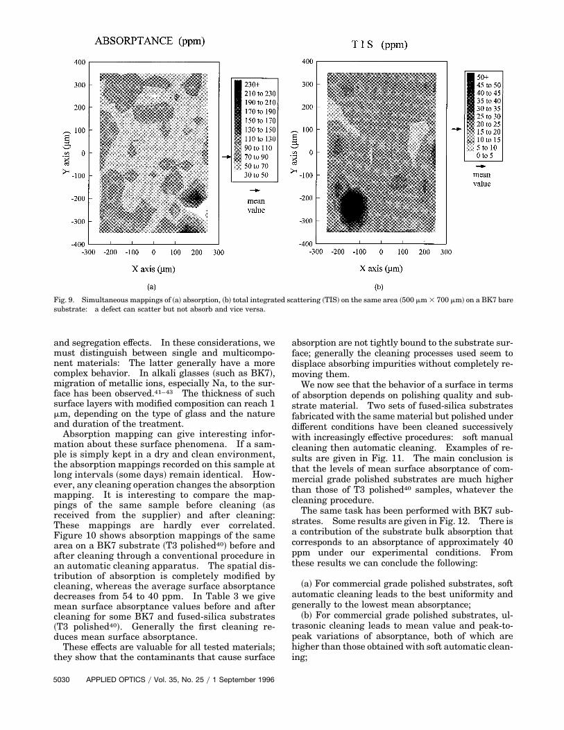
Fig. 9. Simultaneous mappings of ~a! absorption, ~b! total integrated scattering ~TIS! on the same area ~500 mm 3 700 mm! on a BK7 baresubstrate: a defect can scatter but not absorb and vice versa.
and segregation effects. In these considerations, wemust distinguish between single and multicompo-nent materials: The latter generally have a morecomplex behavior. In alkali glasses ~such as BK7!,migration of metallic ions, especially Na, to the sur-face has been observed.41–43 The thickness of suchsurface layers with modified composition can reach 1mm, depending on the type of glass and the natureand duration of the treatment.Absorption mapping can give interesting infor-
mation about these surface phenomena. If a sam-ple is simply kept in a dry and clean environment,the absorption mappings recorded on this sample atlong intervals ~some days! remain identical. How-ever, any cleaning operation changes the absorptionmapping. It is interesting to compare the map-pings of the same sample before cleaning ~asreceived from the supplier! and after cleaning:These mappings are hardly ever correlated.Figure 10 shows absorption mappings of the samearea on a BK7 substrate ~T3 polished40! before andafter cleaning through a conventional procedure inan automatic cleaning apparatus. The spatial dis-tribution of absorption is completely modified bycleaning, whereas the average surface absorptancedecreases from 54 to 40 ppm. In Table 3 we givemean surface absorptance values before and aftercleaning for some BK7 and fused-silica substrates~T3 polished40!. Generally the first cleaning re-duces mean surface absorptance.These effects are valuable for all tested materials;
they show that the contaminants that cause surface
5030 APPLIED OPTICS y Vol. 35, No. 25 y 1 September 1996
absorption are not tightly bound to the substrate sur-face; generally the cleaning processes used seem todisplace absorbing impurities without completely re-moving them.We now see that the behavior of a surface in terms
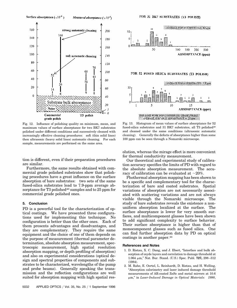
of absorption depends on polishing quality and sub-strate material. Two sets of fused-silica substratesfabricated with the samematerial but polished underdifferent conditions have been cleaned successivelywith increasingly effective procedures: soft manualcleaning then automatic cleaning. Examples of re-sults are given in Fig. 11. The main conclusion isthat the levels of mean surface absorptance of com-mercial grade polished substrates are much higherthan those of T3 polished40 samples, whatever thecleaning procedure.The same task has been performed with BK7 sub-
strates. Some results are given in Fig. 12. There isa contribution of the substrate bulk absorption thatcorresponds to an absorptance of approximately 40ppm under our experimental conditions. Fromthese results we can conclude the following:
~a! For commercial grade polished substrates, softautomatic cleaning leads to the best uniformity andgenerally to the lowest mean absorptance;
~b! For commercial grade polished substrates, ul-trasonic cleaning leads to mean value and peak-to-peak variations of absorptance, both of which arehigher than those obtained with soft automatic clean-ing;

Fig. 10. Absorption mapping of the same area on a BK7 bare substrate ~a! before, ~b! after cleaning by the use of a conventional procedurethrough an automatic cleaning apparatus. The spatial distribution of absorption is completely modified, whereas the average surfaceabsorptance decreases from 54 down to 40 ppm.
~c! On the other hand, the two cleaning proceduresof T3 polished40 substrates give similar results forboth mean and maximum values.
We can see that the cleaning behavior of BK7 sur-faces and their optical performances in terms of ab-sorption are different from those of fused silica.These absorption data bear out results about physicaland chemical properties of glass surfaces.In Fig. 13 we give, in histogram form, the mean
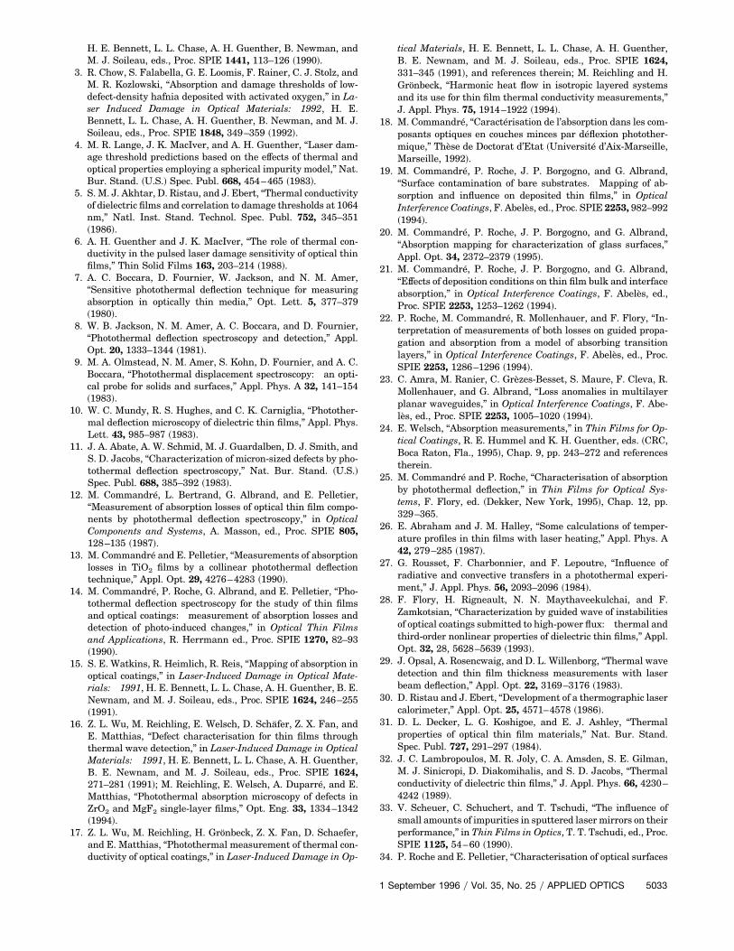
values of surface absorptance of 52 fused-silica and31 BK7 substrates, all T3 polished40 and cleaned withthe same automatic procedure. The mean values ofsurface absorptance for fused-silica substrates rangefrom 3 to 20 ppm. Those measured on BK7 sub-strates vary from 10 to 90 ppm. The average valueis 7.9 ppm for the whole set of fused-silica substratesand 52 ppm for BK7 substrates. The behavior ofthese two kinds of surfaces in terms of optical absorp-
Table 3. Mean Surface Absorptance Values ~ppm! before and afterCleaning for T3 Polished40 Substrates
SubstrateBeforeCleaning
AfterCleaning
Ratio AfteryBefore ~%!
BK7 60 45 7554 40 7460 54 9058 45 78
Fused silica 5.7 6.0 1056.1 5.2 85
Fig. 11. Influence of polishing quality on minimum, mean, andmaximum values of absorption. Example of results for two fused-silica substrates polished in different conditions and successivelycleaned with increasingly effective cleaning procedures are given:soft manual cleaning ~thin solid lines! then ultrasonic automaticcleaning ~heavy solid lines!. For each sample, measurements areperformed on the same area.
1 September 1996 y Vol. 35, No. 25 y APPLIED OPTICS 5031
tion is different, even if their preparation proceduresare similar.Furthermore, the same results obtained with com-
mercial grade polished substrates show that polish-ing procedures have a great influence on the surfaceabsorption of bare substrates: two sets of the samefused-silica substrates lead to 7.9-ppm average ab-sorptance for T3 polished40 samples and to 25 ppm forcommercial grade polished ones.
5. Conclusion
PD is a powerful tool for the characterization of op-tical coatings. We have presented three configura-tions used for implementing this technique. Noconfiguration is better than the other ones. Each ofthem presents advantages and disadvantages, andthey are complementary. They require the sameequipment and the choice of one of them depends onthe purpose of measurement ~thermal parameter de-termination, absolute absorptionmeasurement, spec-troscopic measurement, high spatial resolutionabsorption mapping, or depth profiling of absorption!and also on experimental considerations ~optical de-sign and spectral properties of components and sub-strates to be characterized, wavelengths of the pumpand probe beams!. Generally speaking the trans-mission and the reflection configurations are wellsuited for absorption mapping with high spatial res-
Fig. 12. Influence of polishing quality on minimum, mean, andmaximum values of surface absorptance for two BK7 substratespolished under different conditions and successively cleaned withincreasingly effective cleaning procedures: soft ~thin solid lines!then ultrasonic ~heavy solid lines! automatic cleaning. For eachsample, measurements are performed on the same area.
5032 APPLIED OPTICS y Vol. 35, No. 25 y 1 September 1996
olution, whereas the mirage effect is more convenientfor thermal conductivity measurement.Our theoretical and experimental study of calibra-
tion accuracy specifies the limits of PD with regard tothe absolute absorption measurement. The accu-racy of calibration can be evaluated at ;20%.Phothermal absorptionmapping has been shown to
be a specific and complementary tool for the charac-terization of bare and coated substrates. Spatialvariations of absorption are not necessarily associ-ated with scattering variations and are not alwaysvisible through the Nomarski microscope. Thestudy of bare substrates reveals the existence a non-uniform absorption localized at the surface. Thesurface absorptance is lower for very smooth sur-faces, and multicomponent glasses have been shownto add significant complexity to surface behavior.Their surface absorptance is higher than that ofmonocomponent glasses such as fused silica. Onecan find further absorption data by PD on opticalcoatings in another paper.44
References and Notes1. D. Ristau, X. C. Dang, and J. Ebert, “Interface and bulk ab-
sorption of oxyde layers and correlation to damage threshold at1.064 mm,” Nat. Bur. Stand. ~U.S.! Spec. Publ. 727, 298–312~1984!.
2. M. Rahe, E. Oertel, L. Reinhardt, D. Ristau, and H. Welling,“Absorption calorimetry and laser induced damage thresholdmeasurements of AR-coated ZnSe and metal mirrors at 10.6mm,” in Laser-Induced Damage in Optical Materials: 1990,
Fig. 13. Histogram of mean values of surface absorptance for 52fused-silica substrates and 31 BK7 substrates, all T3 polished40and cleaned under the same conditions ~ultrasonic automaticcleaning!. Generally the defects of absorptance higher than some100 ppm can be seen through a Nomarski microscope.
H. E. Bennett, L. L. Chase, A. H. Guenther, B. Newman, andM. J. Soileau, eds., Proc. SPIE 1441, 113–126 ~1990!.
3. R. Chow, S. Falabella, G. E. Loomis, F. Rainer, C. J. Stolz, andM. R. Kozlowski, “Absorption and damage thresholds of low-defect-density hafnia deposited with activated oxygen,” in La-ser Induced Damage in Optical Materials: 1992, H. E.Bennett, L. L. Chase, A. H. Guenther, B. Newman, and M. J.Soileau, eds., Proc. SPIE 1848, 349–359 ~1992!.
4. M. R. Lange, J. K. MacIver, and A. H. Guenther, “Laser dam-age threshold predictions based on the effects of thermal andoptical properties employing a spherical impurity model,” Nat.Bur. Stand. ~U.S.! Spec. Publ. 668, 454–465 ~1983!.
5. S. M. J. Akhtar, D. Ristau, and J. Ebert, “Thermal conductivityof dielectric films and correlation to damage thresholds at 1064nm,” Natl. Inst. Stand. Technol. Spec. Publ. 752, 345–351~1986!.
6. A. H. Guenther and J. K. MacIver, “The role of thermal con-ductivity in the pulsed laser damage sensitivity of optical thinfilms,” Thin Solid Films 163, 203–214 ~1988!.
7. A. C. Boccara, D. Fournier, W. Jackson, and N. M. Amer,“Sensitive photothermal deflection technique for measuringabsorption in optically thin media,” Opt. Lett. 5, 377–379~1980!.
8. W. B. Jackson, N. M. Amer, A. C. Boccara, and D. Fournier,“Photothermal deflection spectroscopy and detection,” Appl.Opt. 20, 1333–1344 ~1981!.
9. M. A. Olmstead, N. M. Amer, S. Kohn, D. Fournier, and A. C.Boccara, “Photothermal displacement spectroscopy: an opti-cal probe for solids and surfaces,” Appl. Phys. A 32, 141–154~1983!.
10. W. C. Mundy, R. S. Hughes, and C. K. Carniglia, “Photother-mal deflection microscopy of dielectric thin films,” Appl. Phys.Lett. 43, 985–987 ~1983!.
11. J. A. Abate, A. W. Schmid, M. J. Guardalben, D. J. Smith, andS. D. Jacobs, “Characterization of micron-sized defects by pho-tothermal deflection spectroscopy,” Nat. Bur. Stand. ~U.S.!Spec. Publ. 688, 385–392 ~1983!.
12. M. Commandre, L. Bertrand, G. Albrand, and E. Pelletier,“Measurement of absorption losses of optical thin film compo-nents by photothermal deflection spectroscopy,” in OpticalComponents and Systems, A. Masson, ed., Proc. SPIE 805,128–135 ~1987!.
13. M. Commandre and E. Pelletier, “Measurements of absorptionlosses in TiO2 films by a collinear photothermal deflectiontechnique,” Appl. Opt. 29, 4276–4283 ~1990!.
14. M. Commandre, P. Roche, G. Albrand, and E. Pelletier, “Pho-tothermal deflection spectroscopy for the study of thin filmsand optical coatings: measurement of absorption losses anddetection of photo-induced changes,” in Optical Thin Filmsand Applications, R. Herrmann ed., Proc. SPIE 1270, 82–93~1990!.
15. S. E. Watkins, R. Heimlich, R. Reis, “Mapping of absorption inoptical coatings,” in Laser-Induced Damage in Optical Mate-rials: 1991, H. E. Bennett, L. L. Chase, A. H. Guenther, B. E.Newnam, and M. J. Soileau, eds., Proc. SPIE 1624, 246–255~1991!.
16. Z. L. Wu, M. Reichling, E. Welsch, D. Schafer, Z. X. Fan, andE. Matthias, “Defect characterisation for thin films throughthermal wave detection,” in Laser-Induced Damage in OpticalMaterials: 1991, H. E. Bennett, L. L. Chase, A. H. Guenther,B. E. Newnam, and M. J. Soileau, eds., Proc. SPIE 1624,271–281 ~1991!; M. Reichling, E. Welsch, A. Duparre, and E.Matthias, “Photothermal absorption microscopy of defects inZrO2 and MgF2 single-layer films,” Opt. Eng. 33, 1334–1342~1994!.
17. Z. L. Wu, M. Reichling, H. Gronbeck, Z. X. Fan, D. Schaefer,and E. Matthias, “Photothermal measurement of thermal con-ductivity of optical coatings,” in Laser-Induced Damage in Op-
tical Materials, H. E. Bennett, L. L. Chase, A. H. Guenther,B. E. Newnam, and M. J. Soileau, eds., Proc. SPIE 1624,331–345 ~1991!, and references therein; M. Reichling and H.Gronbeck, “Harmonic heat flow in isotropic layered systemsand its use for thin film thermal conductivity measurements,”J. Appl. Phys. 75, 1914–1922 ~1994!.
18. M. Commandre, “Caracterisation de l’absorption dans les com-posants optiques en couches minces par deflexion photother-mique,” These de Doctorat d’Etat ~Universite d’Aix-Marseille,Marseille, 1992!.
19. M. Commandre, P. Roche, J. P. Borgogno, and G. Albrand,“Surface contamination of bare substrates. Mapping of ab-sorption and influence on deposited thin films,” in OpticalInterference Coatings, F. Abeles, ed., Proc. SPIE 2253, 982–992~1994!.
20. M. Commandre, P. Roche, J. P. Borgogno, and G. Albrand,“Absorption mapping for characterization of glass surfaces,”Appl. Opt. 34, 2372–2379 ~1995!.
21. M. Commandre, P. Roche, J. P. Borgogno, and G. Albrand,“Effects of deposition conditions on thin film bulk and interfaceabsorption,” in Optical Interference Coatings, F. Abeles, ed.,Proc. SPIE 2253, 1253–1262 ~1994!.
22. P. Roche, M. Commandre, R. Mollenhauer, and F. Flory, “In-terpretation of measurements of both losses on guided propa-gation and absorption from a model of absorbing transitionlayers,” in Optical Interference Coatings, F. Abeles, ed., Proc.SPIE 2253, 1286–1296 ~1994!.
23. C. Amra, M. Ranier, C. Grezes-Besset, S. Maure, F. Cleva, R.Mollenhauer, and G. Albrand, “Loss anomalies in multilayerplanar waveguides,” in Optical Interference Coatings, F. Abe-les, ed., Proc. SPIE 2253, 1005–1020 ~1994!.
24. E. Welsch, “Absorption measurements,” in Thin Films for Op-tical Coatings, R. E. Hummel and K. H. Guenther, eds. ~CRC,Boca Raton, Fla., 1995!, Chap. 9, pp. 243–272 and referencestherein.
25. M. Commandre and P. Roche, “Characterisation of absorptionby photothermal deflection,” in Thin Films for Optical Sys-tems, F. Flory, ed. ~Dekker, New York, 1995!, Chap. 12, pp.329–365.
26. E. Abraham and J. M. Halley, “Some calculations of temper-ature profiles in thin films with laser heating,” Appl. Phys. A42, 279–285 ~1987!.
27. G. Rousset, F. Charbonnier, and F. Lepoutre, “Influence ofradiative and convective transfers in a photothermal experi-ment,” J. Appl. Phys. 56, 2093–2096 ~1984!.
28. F. Flory, H. Rigneault, N. N. Maythaveekulchai, and F.Zamkotsian, “Characterization by guided wave of instabilitiesof optical coatings submitted to high-power flux: thermal andthird-order nonlinear properties of dielectric thin films,” Appl.Opt. 32, 28, 5628–5639 ~1993!.
29. J. Opsal, A. Rosencwaig, and D. L. Willenborg, “Thermal wavedetection and thin film thickness measurements with laserbeam deflection,” Appl. Opt. 22, 3169–3176 ~1983!.
30. D. Ristau and J. Ebert, “Development of a thermographic lasercalorimeter,” Appl. Opt. 25, 4571–4578 ~1986!.
31. D. L. Decker, L. G. Koshigoe, and E. J. Ashley, “Thermalproperties of optical thin film materials,” Nat. Bur. Stand.Spec. Publ. 727, 291–297 ~1984!.
32. J. C. Lambropoulos, M. R. Joly, C. A. Amsden, S. E. Gilman,M. J. Sinicropi, D. Diakomihalis, and S. D. Jacobs, “Thermalconductivity of dielectric thin films,” J. Appl. Phys. 66, 4230–4242 ~1989!.
33. V. Scheuer, C. Schuchert, and T. Tschudi, “The influence ofsmall amounts of impurities in sputtered lasermirrors on theirperformance,” in Thin Films in Optics, T. T. Tschudi, ed., Proc.SPIE 1125, 54–60 ~1990!.
34. P. Roche and E. Pelletier, “Characterisation of optical surfaces
1 September 1996 y Vol. 35, No. 25 y APPLIED OPTICS 5033
by measurement of scattering distribution,” Appl. Opt. 23,3561–3566 ~1984!.
35. P. A. Temple, “Examination of laser damage sites of transpar-ent surfaces and films using total internal reflection microsco-py,” in Laser Induced Damage in Optical Materials: 1979,Nat. Bur. Stand. Spec. Publ. 568, 333–341 ~1979!.
36. F. L. Williams, C. K. Carniglia, B. J. Pond, and W. K. Stowell,“Investigation of thin films using total internal reflection mi-croscopy,” in Laser Induced Damage in Optical Materials:1989, Nat. Inst. Stand. Technol. Spec. Publ. 801, 299–308~1989!.
37. R. C. Estier, N. S. Nogar, and R. A. Schmell, “The detection,removal and effect on damage thresholds of cerium impuritieson fused silica,” in Laser Induced Damage in Optical Materi-als: 1988, Nat. Inst. Stand. Technol. Spec. Publ. 775, 183–188 ~1988!.
38. T. Raj, D. E. McCready, and C. K. Carniglia, “Substrate clean-ing in vacuum by laser irradiation,” in Laser Induced Damage
5034 APPLIED OPTICS y Vol. 35, No. 25 y 1 September 1996
in Optical Materials: 1988, Nat. Inst. Stand. Technol. Spec.Publ. 775, 152–165 ~1988!.
39. R. S. Hockett, “Quantitative analysis of surface trace metalcontamination on substrates and films by TXRF,” in LaserInduced Damage in Optical Materials: 1989, Nat. Inst.Stand. Technol. Spec. Publ. 801, 239–253 ~1989!.
40. Very smooth surface finish ~French Standard NF S 10-006!.The rms roughness is ;0.3 nm.
41. H. K. Pulker, “Nature of a surface,” in Coating on Glass~Elsevier, New York, 1984!, Chap 3, pp. 34–42.
42. T. S. Izumitani, Optical Glass, American Institute of PhysicsTranslation Series ~American Institute of Physics, New York,1986!, Chap. 2, pp. 15–55.
43. K. Kinosita, “Surface deterioration of optical glasses,” inProgress in Optics, E. Wolf, ed. ~North-Holland, Amsterdam,1965!, Vol. 4, pp. 85–143.
44. P. Roche, M. Commandre, L. Escoubas, J. P. Borgogno, G.Albrand, and B. Lazarides, “Substrate effects on absorption ofcoated surfaces,” Appl. Opt. 35, 5059–5066 ~1996!.


![Dangc Pds 71 Pds Ngc Model700[1]](https://img.pdfslide.net/doc/110x75/577cc1111a28aba71192272d/dangc-pds-71-pds-ngc-model7001.jpg)