Embed Size (px)
Citation preview

SANDIA REPORTSAND2002-0340Unlimited ReleasePrinted March 2002
Characterization of SF6 / Argon Plasmasfor Microelectronics Applications
G. A. Hebner, I. G. Abraham, and J. R. Woodworth
Prepared bySandia National LaboratoriesAlbuquerque, New Mexico 87185 and Livermore, California 94550
Sandia is a multiprogram laboratory operated by Sandia Corporation,a Lockheed Martin Company, for the United States Department ofEnergy under Contract DE-AC04-94AL85000.
Approved for public release; further dissemination unlimited.

Issued by Sandia National Laboratories, operated for the United States Departmentof Energy by Sandia Corporation.
NOTICE: This report was prepared as an account of work sponsored by an agencyof the United States Government. Neither the United States Government, nor anyagency thereof, nor any of their employees, nor any of their contractors,subcontractors, or their employees, make any warranty, express or implied, orassume any legal liability or responsibility for the accuracy, completeness, orusefulness of any information, apparatus, product, or process disclosed, or representthat its use would not infringe privately owned rights. Reference herein to anyspecific commercial product, process, or service by trade name, trademark,manufacturer, or otherwise, does not necessarily constitute or imply its endorsement,recommendation, or favoring by the United States Government, any agency thereof,or any of their contractors or subcontractors. The views and opinions expressedherein do not necessarily state or reflect those of the United States Government, anyagency thereof, or any of their contractors.
Printed in the United States of America. This report has been reproduced directlyfrom the best available copy.
Available to DOE and DOE contractors fromU.S. Department of EnergyOffice of Scientific and Technical InformationP.O. Box 62Oak Ridge, TN 37831
Telephone: (865)576-8401Facsimile: (865)576-5728E-Mail: [email protected] ordering: http://www.doe.gov/bridge
Available to the public fromU.S. Department of CommerceNational Technical Information Service5285 Port Royal RdSpringfield, VA 22161
Telephone: (800)553-6847Facsimile: (703)605-6900E-Mail: [email protected] order: http://www.ntis.gov/ordering.htm

1
SAND2002-0340 Unlimited Release
Printed March 2002
Characterization of SF6 / Argon plasmas for
microelectronics applications
Gregory. A. Hebner, Ion. C. Abraham and Joseph. R. Woodworth
Plasma Sciences Department Sandia National Laboratories
P.O. Box 5800 Albuquerque, NM 87185-1423
Abstract
This report documents measurements in inductively driven plasmas containing SF6 / Argon gas mixtures. The data in this report is presented in a series of appendices with a minimum of interpretation. During the course of this work we investigated: the electron and negative ion density using microwave interferometry and laser photodetachment; the optical emission; plasma species using mass spectrometry, and the ion energy distributions at the surface of the rf biased electrode in several configurations. The goal of this work was to assemble a consistent set of data to understand the important chemical mechanisms in SF6 based processing of materials and to validate models of the gas and surface processes.

2
Table of contents Project overview ………………………………………………………….………3 Appendix 1. Optical emission………………………………………………………………4 2. Plasma species determined by mass spectrometry……………………………15 3. Electron and negative ion density……………………………………………..33 4. Ion energy at the surface with surface features………………………………..60

3
Project Overview The purpose of this report is to document measurements in inductively driven plasmas containing SF6 / Argon gas mixtures. During the course of this work a number of measurements were performed to begin to assemble a consistent set of data to 1) understand the important physical and chemical mechanisms active in SF6 based processing of microelectronic materials and 2) to generate a data set to validate models of the gas and surface processes, including feature evolution. While SF6 has been used for many years in plasma processes, there is a significant lack of fundamental data of the type required to validate models. Results from the various measurements are presented in a series of appendices. The appendices include a brief description of the measurement technique and then the data. In many cases, there is a minimum of interpretation. Appendix 1 includes the results of optical emission measurements of SF6 gas mixtures over a range of powers and pressures. Appendix 2 reviews data obtained using a mass spectrometer. A mass spectrometer was used to survey the ion and neutral species present in the plasma and in the case of ion species, measure the scaling with plasma condition. Appendix 3 is a preprint of a paper submitted to the Journal of Applied Physics on measurements of the electron and negative ion density in SF6 / Ar gas mixtures. Appendix 4 is a preprint of a paper submitted to the Journal of Vacuum Science and Technology A on measurements of the ion energy at the surface of a rf biased electrode with surface features. Finally, we note that this work was the outgrowth of a funds-in CRADA with Motorola Corporation. We appreciate their support and access to their problems. The authors acknowledge the contributions of P. A. Miller, R. J. Shul, I. C. Abraham, B. P. Aragon, T. W. Hamilton and C. G. Willison to this work. This work was performed at Sandia National Laboratories and supported by Motorola and Sandia National Laboratories. Sandia is a multiprogram laboratory operated by Sandia Corporation, a Lockheed Martin Company, for the United States Department of Energy under contract DE-AC04-94AL85000.

4
Appendix 1
Optical Emission Measurements In Ar/SF6/C4F8 Discharges
Experimental Conditions
The experiments were performed in the GEC Reference Cell. The Cell had the
anodized Al ICP window holder and the fused silica ring in place. Two wafer surfaces,
silicon and oxide (fused silica) wafer were used.
Two mixtures of Ar/SF6, 10/90 and 50/50, and pure C4F8 discharges were
investigated. The 10/90 Ar/SF6 mixture was investigated using actinometry (F atom line
at 703.75 nm intensity ratio vs. Ar atom line at 750.39 nm). We could not sustain a pure
SF6 discharge with the oxide wafer in place. The center of the matrix of power and
pressure conditions was at 10 mTorr total pressure, 10 sccm total flow rate, 200 W ICP
coil power, and 20 W rf-bias power.
The light emitted from the plasma was dispersed using a Jobin HR460
monochromator with a 50 µm slit width, and a 300 lines/mm grating, and detected using
a Princeton Instruments camera, set for 0.1 or 0.5 s exposure times, depending on the line
intensities in the particular region. Six spectral regions, spanning from 190 nm to 850
nm, were calibrated using Ne, Ar, Kr, and Hg lamps.
The following 14 pages contains our optical emission data. In the trend plots vs.
power, pressure, and rf-bias, the series marked “broad” is an integrated signal level for
particular regions in the spectra with no detectable line features, just a broad emission
envelope, which may be correlated with SiF3 or CF3 (in C4F8 plasmas). One region was
integrated for Ar/SF6 plasmas, from 340-380 nm, and three regions were integrated and
added together for C4F8 plasmas, from 240-280 nm, from 340-355 nm, and from 640-660
nm. The wavelengths that were used for the other species identified in the trend plots
were: SiF = 440 nm, SiF2 = 390.15 nm, SFx = 289.3 nm, Si = 576.3 nm. In order to show
the trends for different species whose emission intensities could vary by orders of
magnitude on the same graph, the intensities were scaled such that the highest intensity
for a given emitting species in a given trend was assigned a value of 1.0, with the
emission intensity of that species at the other conditions in the trend being
proportionately smaller.

5
10/90 Ar/SF6 10 mTorr 200 W ICP coil power 20 W rf-bias power silicon wafer
10 % Ar / SF6 OES Silicon10 mTorr 200 W / 20 W
0
500,000
1,000,000
1,500,000
2,000,000
2,500,000
3,000,000
3,500,000
4,000,000
4,500,000
5,000,000
2000 2500 3000 3500 4000 4500 5000 5500 6000 6500 7000 7500 8000 8500
Wavelength (Angstrom)
Inte
nsity
(arb
. uni
ts)
OES Pressure Dependence10 % Ar / SF6 on Si
0
0.2
0.4
0.6
0.8
1
1.2
0 5 10 15 20 25
Pressure (mTorr)
Scal
ed In
tens
ity
F atomSiFSiF2SFxSiF/ArBroad

6
OES Inductive Power Dependence10 % Ar / SF6 on Si
0
0.2
0.4
0.6
0.8
1
1.2
0 50 100 150 200 250 300 350
Power (Watts)
Scal
ed In
tens
ity
F atomSiFSiF2SFxSiF/ArBroad
OES Bias Power Dependence10 % Ar / SF6 on Si
0
0.2
0.4
0.6
0.8
1
1.2
0 20 40 60 80 100 120
Bias Power (Watts)
Scal
ed In
tens
ity
F atomSiFSiF2SFxSiF/ArBroad

7
50/50 Ar/SF6 10 mTorr 200 W ICP coil power 20 W rf-bias power silicon wafer
50 / 50 Ar / SF6 OES Silicon10 mTorr 200 W / 20 W
0
1,000,000
2,000,000
3,000,000
4,000,000
5,000,000
6,000,000
7,000,000
8,000,000
9,000,000
10,000,000
2000 2500 3000 3500 4000 4500 5000 5500 6000 6500 7000 7500 8000 8500
Wavelength (Angstrom)
Inte
nsity
(arb
. uni
ts)
OES Inductive Power Dependence50 / 50 Ar / SF6 on Si
0
0.2
0.4
0.6
0.8
1
1.2
0 50 100 150 200 250 300 350
Power (Watts)
Scal
ed In
tens
ity
F atomSiFSiF2SFxSiBroad

8
OES Expanded Pressure Dependence50 / 50 Ar / SF6 on Si
0
0.2
0.4
0.6
0.8
1
1.2
0 5 10 15 20 25 30 35
Pressure (mTorr)
Scal
ed In
tens
ity
F atomSiFSiF2SFxSiBroad
OES Bias Power Dependence50 / 50 Ar / SF6 on Si
0
0.2
0.4
0.6
0.8
1
1.2
0 20 40 60 80 100 120
Bias Power (Watts)
Scal
ed In
tens
ity
F atomSiFSiF2SFxSiBroad

9
50/50 Ar/SF6 10 mTorr 200 W ICP coil power 20 W rf-bias power quartz wafer
50/50 Ar / SF6 OES Oxide10 mTorr 200 W / 20 W
0
1,000,000
2,000,000
3,000,000
4,000,000
5,000,000
6,000,000
7,000,000
8,000,000
9,000,000
10,000,000
2000 2500 3000 3500 4000 4500 5000 5500 6000 6500 7000 7500 8000 8500
Wavelength (Angstrom)
Inte
nsity
(arb
. uni
ts)
OES Expanded Pressure Dependence50 / 50 Ar / SF6 on Oxide
0
0.2
0.4
0.6
0.8
1
1.2
0 5 10 15 20 25 30 35
Pressure (mTorr)
Scal
ed In
tens
ity
F atomSiFSiF2SFxSiOBroad

10
OES Inductive Power Dependence50 / 50 Ar / SF6 on Oxide
0
0.2
0.4
0.6
0.8
1
1.2
0 50 100 150 200 250 300 350
Power (Watts)
Scal
ed In
tens
ity
F atomSiFSiF2SFxSiOBroad
OES Bias Power Dependence50 / 50 Ar / SF6 on Oxide
0
0.2
0.4
0.6
0.8
1
1.2
0 20 40 60 80 100 120
Bias Power (Watts)
Scal
ed In
tens
ity
F atomSiFSiF2SFxSiOBroad
11
C4F8 Plasma 10 mTorr 200 W ICP coil power 20 W rf-bias power silicon wafer
C4F8 OES Silicon10 mTorr 200 W / 20 W
0
500,000
1,000,000
1,500,000
2,000,000
2,500,000
3,000,000
3,500,000
4,000,000
4,500,000
5,000,000
2000 2500 3000 3500 4000 4500 5000 5500 6000 6500 7000 7500 8000 8500
Wavelength (Angstrom)
Inte
nsity
(arb
. uni
ts)
OES Pressure DependenceC4F8 on Si
0
0.2
0.4
0.6
0.8
1
1.2
0 5 10 15 20 25
Pressure (mTorr)
Scal
ed In
tens
ity
F atomSiFSiF2SiCF2CFC2Broad

12
OES Inductive Power DependenceC4F8 on Si
0
0.2
0.4
0.6
0.8
1
1.2
0 50 100 150 200 250 300 350
Power (Watts)
Scal
ed In
tens
ity
F atomSiFSiF2SiCF2CFC2Broad
OES Bias Power DependenceC4F8 on Si
0
0.2
0.4
0.6
0.8
1
1.2
0 20 40 60 80 100 120
Bias Power (Watts)
Scal
ed In
tens
ity
F atomSiFSiF2SiCF2CFC2Broad

13
C4F8 Plasma 10 mTorr 200 W ICP coil power 20 W rf-bias power quartz wafer
C4F8 OES Oxide10 mTorr 200 W / 20 W
0
500,000
1,000,000
1,500,000
2,000,000
2,500,000
3,000,000
3,500,000
4,000,000
4,500,000
5,000,000
2000 2500 3000 3500 4000 4500 5000 5500 6000 6500 7000 7500 8000 8500
Wavelength (Angstrom)
Inte
nsity
(arb
. uni
ts)
OES Pressure DependenceC4F8 on Oxide
0
0.2
0.4
0.6
0.8
1
1.2
0 5 10 15 20 25
Pressure (mTorr)
Scal
ed In
tens
ity
F atomSiFSiF2SiCF2C2Broad

14
OES Inductive Power DependenceC4F8 on Oxide
0
0.2
0.4
0.6
0.8
1
1.2
0 50 100 150 200 250 300 350
Power (Watts)
Scal
ed In
tens
ity
F atomSiFSiF2SiCF2C2Broad
OES Bias Power DependenceC4F8 on Oxide
0
0.2
0.4
0.6
0.8
1
1.2
0 20 40 60 80 100 120
Bias Power (Watts)
Scal
ed In
tens
ity
F atomSiFSiF2SiCF2C2Broad

15
Appendix 2
Mass Spectrometer / Ion Energy Analyzer Measurements in Ar/SF6 Discharges
Experimental Conditions
The experiments were performed in the GEC Reference Cell. The Cell had the
anodized Al ICP window holder and the fused silica ring in place. The Balzers mass
spectrometer had a 25 µm pinhole installed. The Balzers instrument can scan either
across a mass or energy range, but not both at the same time. This means that for a mass
scan of ions, a given ion energy had to be selected.
The data is shown in the next 17 pages. For the mass scan surveys of ions and
neutrals, the conditions were 15 mTorr total pressure, 200 W ICP coil power, and 30 W
of chuck power, both at 13.56 MHz and phase locked to each other. The applied rf-bias
power to the chuck produced an applied voltage of 63 Vpp, as measured by a capacitive
voltage sensor. A 6” silicon wafer (with a 1 cm diameter hole in the center) was placed
on the chuck during these experiments. For the mass scans of ions, the energy analyzer
was set for 40 eV ions. Three mixtures of Ar/SF6/O2 were surveyed: 50/45/5, 50/25/25,
and 0/90/10, with 20 sccm total flowrate. For the mass scan of neutrals, the total flow
rate was again 20 sccm and the mixtures of Ar/SF6/O2 investigated were 50/45/5,
50/25/25, and 90/10/0. Ion energy distributions were measured for the 50/45/5 mixture
for SF+, SF3+, and SF5
+. The neutral molecules were ionized in the spectrometer with a
100 eV electron beam prior to detection.
Relative total ion fluxes of Ar+ and SFx+ (x = 1-5) ions were measured at 10
mTorr total pressure, and 240 W and 360 W ICP coil power for mixtures of 50/50 and
90/10 Ar/SF6 and 10 sccm total flow rate using a 2 mm thick fused silica (SiO2) wafer, in
order to minimize etching. Only a small rf-bias (2 W) was applied to the chuck in order
to prevent sulfur deposits on the chuck and pinhole. The experiment was repeated at 240
W ICP coil power twice for the 50/50 Ar/SF6 mixture and once for the 90/10 mix. A
similar experiment was carried out using a silicon wafer and the 90/10 mix at 240 W and
360 W ICP coil power, again at 10 mTorr total pressure and 10 sccm total flow rate. For
the silicon wafer experiment, the data includes relative fluxes of the etch products SiFx+
(x = 1,2).

16
Ions, 40 eV Ar/SF6/O2 50/45/5
Ions 40 eV 50/45/5
100
1000
10000
100000
1000000
0 20 40 60 80 100 120 140 160 180 200
mass (amu)
Ion
Flux
(cps
)

17
Ions 40 eV 50/45/5
100
1000
10000
100000
1000000
45 50 55 60 65 70 75
mass (amu)
Ion
Flux
(cps
)
SiF+
SO+SiF+
S2+ SiF2+
SF2+
Ions 40 eV 50/45/5
100
1000
10000
100000
1000000
75 80 85 90 95 100 105 110 115
mass (amu)
Ion
Flux
(cps
)
SO4+
SiF3+
SiF4+
SF3+
Ions 40 eV 50/45/5
100
1000
10000
100000
1000000
75 80 85 90 95 100 105 110 115
mass (amu)
Ion
Flux
(cps
)
SO4+
SiF3+
SiF4+
SF3+

18
Ions 40 eV 50/45/5
100
1000
10000
100000
1000000
115 120 125 130 135 140 145 150
mass (amu)
Ion
Flux
(cps
)
SF5+

19
Ions, 40 eV Ar/SF6/O2 50/25/25
Ions 40 eV 50/25/25
100
1000
10000
100000
1000000
0 20 40 60 80 100 120 140 160 180 200
mass (amu)
Ion
Flux
(cps
)

20
Ions 40 eV 50/25/25
100
1000
10000
100000
1000000
45 50 55 60 65 70 75
mass (amu)
Ion
Flux
(cps
)
SiF+
SO+
SF+S2+
SiF2+SF2+
Ions 40 eV 50/25/25
100
1000
10000
100000
1000000
75 80 85 90 95 100 105 110 115
mass (amu)
Ion
Flux
(cps
)
SiF3+
SiF4+SF3+

21
Ions 40 eV 50/25/25
100
1000
10000
100000
1000000
115 120 125 130 135 140 145 150
mass (amu)
Ion
Flux
(cps
)
SF5+

22
Ions, 40 eV Ar/SF6/O2 0/90/10
Ions 40 eV 0/90/10
100
1000
10000
100000
1000000
0 20 40 60 80 100 120 140 160 180 200
mass (amu)
Ion
Flux
(cps
)

23
Ions 40 eV 0/90/10
100
1000
10000
100000
1000000
45 50 55 60 65 70 75
mass (amu)
Ion
Flux
(cps
)
SiF+
SF+
S2+SiF2+
SF2+
Ions 40 eV 0/90/10
100
1000
10000
100000
1000000
75 80 85 90 95 100 105 110 115
mass (amu)
Ion
Flux
(cps
)
SiF3+
SF3+

24
Ions 40 eV 0/90/10
100
1000
10000
100000
1000000
115 120 125 130 135 140 145 150
mass (amu)
Ion
Flux
(cps
)
SF5+

25
Neutrals Ar/SF6/O2 50/45/5
Neutrals 50/45/5
100
1000
10000
100000
1000000
0 20 40 60 80 100 120 140 160 180 200
mass (amu)
Ion
Flux
(cps
)

26
Neutrals 50/45/5
0
50000
100000
150000
200000
250000
300000
350000
400000
45 50 55 60 65 70 75 80 85 90 95 100
mass (amu)
Ion
Flux
(cps
)
SiF3
SF2
SiF
S2
SFSF3

27
Neutrals Ar/SF6/O2 50/25/25
Neutrals 50/25/25
100
1000
10000
100000
1000000
10000000
0 20 40 60 80 100 120 140 160 180 200
mass (amu)
Ion
Flux
(cps
)
Neutrals 50/25/25
100
1000
10000
100000
1000000
10000000
45 55 65 75 85 95
mass (amu)
Ion
Flux
(cps
)
SOSO2
SO3
SiF3
SOFSF2

28
Neutrals 50/25/25
100
1000
10000
100000
1000000
10000000
100 105 110 115 120 125 130 135 140 145 150
mass (amu)
Ion
Flux
(cps
)
SF4SiF4
SF5
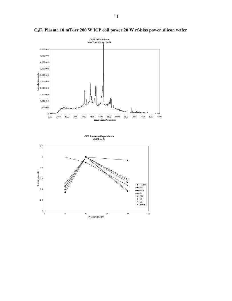
Neutrals Ar/SF6/O2 90/10/0
Neutrals 90/10/0
100
1000
10000
100000
1000000
10000000
0 20 40 60 80 100 120 140 160 180 200
mass (amu)
Ion
Flux
(cps
)
29
Neutrals 90/10/0
100
1000
10000
100000
1000000
10000000
45 55 65 75 85 95
mass (amu)
Ion
Flux
(cps
)
SiF3S2 orSO2SO
Neutrals 90/10/0
100
1000
10000
100000
1000000
10000000
100 105 110 115 120 125 130 135 140 145 150
mass (amu)
Ion
Flux
(cps
)
SiF4SF5

30
Relative Ion Flux SiO2 Wafer
Relative Ion Counts at 10 mTorrSiO2 Wafer
1.E+03
1.E+04
1.E+05
1.E+06
1.E+07
1.E+08
240 W 50/50 240 W 90/10 360 W 50/50 360 W 90/10
Inte
nsity
(cps
)
Ar+
SF+
SF2+
SF3+
SF4+
SF5+ A
r+
SF+
SF2+
SF3+
SF4+
SF5+ Ar+
SF+
SF2+
SF3+
SF4+
SF5+
Ar+
SF+
SF2+
SF3+
SF4+
SF5+
Relative Ion Flux SiO2 Wafer Repeat

31
Relative Ion Counts at 10 mTorrSiO2 Wafer Repeat
1.E+03
1.E+04
1.E+05
1.E+06
1.E+07
1.E+08
240 W 50/50 240 W 50/50 240 W 90/10
Inte
nsity
(cps
)
Ar+
SF+
SF2+
SF3+
SF4+
SF5+ Ar+
SF+
SF2+
SF3+
SF4+
SF5+
Ar+
SF+
SF2+
SF3+
SF4+
SF5+
Relative Ion Flux Si Wafer

32
Relative Ion Counts at 10 mTorrSi Wafer
1.E+02
1.E+03
1.E+04
1.E+05
1.E+06
1.E+07
1.E+08
240 W 90/10 360 W 90/10
Inte
nsity
(cps
)
Ar+
SF+
SF2+
SF3+
SF4+
SF5+
SiF2
+
SiF+ A
r+
SF+
SF2+
SF3+
SF4+
SF5+
SiF2
+
SiF+
SFx+ Ion Energy Distributions Ar/SF6/O2 50/45/5
SFx+ Ion Energy Distributions
50/45/5
0
20000
40000
60000
80000
100000
120000
0 10 20 30 40 50 6
Ion Energy (eV)
Ion
Flux
(cps
)
SF5+
SF3+
SF+
0

33
Appendix 3
Surface dependent electron and negative ion density in SF6 / Argon gas mixtures
I. Introduction
Electrically driven plasmas containing halogens are commonly used in a number
of material modification and surface cleaning processes. For example, discharges
containing SF6 and the many varieties of fluorocarbon gases, CxFyHz, are used to etch
silicon or silicon dioxide for microelectronic feature definition. These gases serve as rich
sources of atomic fluorine to etch material. In addition, the fluorocarbon gases also
supply CxFy radicals for sidewall passivation and protection during deep trench etching.
However, in cases where sidewall passivation is not required or is provided by another
process, the use of SF6 is common, as in the Bosch process.1
To understand the critical chemical mechanisms in negative ion containing
plasmas, it is important to determine both the electron and negative ion densities. In such
plasmas, the electron and negative ion density are fundamental plasma parameters that
are influenced by a number of gas and surface reactions. Negative ion formation serves
as a loss mechanism for electrons, and because negative ions tend to collect in regions of
maximum plasma potential, they can serve as a significant loss term for volumetric ion-
ion recombination with positive ions. Negative ions can also influence the sheath voltage
and kinetics, and in the case of pulsed discharge systems, possibly influence the surface
charge. At a more fundamental level, electron and negative ion interactions can alter the
electron energy distribution function, affect the spatial distribution of the plasma
potential, and by charge neutrality, influence the total positive ion charge density. This
in turn can impact the ion flux and ion energy to the wafer surface. Finally,
measurements of the electron and negative ion densities can be used, along with

34
additional measurements, to benchmark and validate recent computer models and to test
radical species chemical reaction mechanisms.2
A key aspect of most plasma processes is that some type of work, such as etching
or cleaning, is done at the plasma / surface boundary layer. As understanding of the
important processes that occur at the plasma / surface boundary layer has improved, we
now realize that etch product chemistry must also be included in both experiments and
models to capture a complete picture of surface profile evolution. For example, a typical
etch rate of 500 nm / min translates into a etch product gas flow from the surface of
approximately 40 sccm for an 8 inch diameter wafer. A gas flow of 40 sccm is a
significant fraction of the total gas flow rate in most processing tools. Radical species
that are evolved from the surface into the gas phase will fully participate in the myriad of
gas phase and surface reactions that are associated with the parent fluorocarbon gas.
Those processes include negative ion formation, electron dissociation, ionization which
contributes to the charge balance, molecular quenching of the electron temperature, and
ion surface bombardment. Thus it is important that more experiments focus on the
influence of surface material and that models begin to incorporate etch products in a self
consistent manner. This clearly increases the complexity of the problem but is the only
way to capture all of the appropriate physics.
There have been a number of measurements of the electron and negative ion
density in SF6, although few reported in inductively driven plasmas (ICP).3,4,5,6,7,8
Kimura and Ohe recently reported probe measurements in SF6 / Xe gas mixtures in an
ICP.3 They reported electron densities on the order of 5 x 1010 cm-3 , and negative ion
densities approximately 5 times higher at moderate powers of 80 W. Kono and
coworkers measured the electron and negative ion density in a capacitively coupled

35
parallel plate chamber using a microwave cavity technique and laser photodetachment.4
At relatively low input powers of 10 W and pressures of less than 100 mTorr, they
measured electron densities on the order of 109 cm-3 and negative ion densities a factor of
100 higher. St-Onge and coworkers performed laser photodetachment measurements in
SF6 containing magnetoplasmas.5 They measured a negative ion / electron density ratio
of 2 to 5 for pressures of 0.2 to 4 mTorr in the region downstream from their microwave
source. This work also includes a good description of the challenges associated with
accurate negative ion identification and the subsequent assignment of absolute densities
to the measured photodetachment signal.
This investigation is an extension of our recent measurements of the electron and
negative ion density in inductively driven discharges containing C2F6, CHF3, and C4F8
9,10 The current work focuses on electron and negative ion densities in SF6 / Ar gas
mixtures as well as voltage and current measurements. We study power densities in the
range of 0.1 to 1 W/cm3 where molecular disassociation tends to be larger than previous
work. In addition to measuring the electron and negative ion density in SF6 / Ar gas
mixtures, this study also investigated the influence of surface material on the electron and
negative ion density. The rf biased wafer surface was covered with either a bare silicon
wafer or a 1-mm-thick fused silica wafer to provide a uniform SiO2 surface. Our
previous work in Cl2 / BCl3, and C4F8 containing discharges showed significant
differences in the electron and negative ion densities above different surface
materials.10,11
II. Experimental setup

36
Experiments were performed in a Gaseous Electronics Conference (GEC) rf
reference cell which was modified to include an inductively coupled plasma (ICP)
source.12,13 Briefly, the induction coil was constructed from 3.2 mm diameter copper
tubing which was wound into a five-turn planar coil 11 cm in diameter, and was water
cooled. In this work, the coil was excited at 13.56 MHz. The coil was separated from
the plasma by a 1-cm-thick fused silica window. The spacing between the window and
the lower electrode was 3.8 cm. For these experiments, the lower electrode was rf biased
(13.56 MHz) and covered with either a 6 inch diameter, 0.6 mm thick, silicon wafer or a
6 inch diameter, 1 mm thick, fused silica (SiO2) wafer. The wafers rested on the lower
electrode without clamping. The lower electrode was water cooled; however, the reactor
was run with a discharge (SF6 or O2) for 30 minutes to reach a steady-state temperature
and wall condition before any measurements were made. For these experiments an
additional modification was made to the GEC chamber; a fused silica ring was clamped
to the upper electrode assembly. The fused silica confinement ring served to stabilize
and extend the operating parameter space of the electronegative discharges. Without the
ring in place, the discharge could only be sustained over a narrow range of power and
pressure. The ring had an inner diameter of 4.5 inches, outer diameter of 6.5 inches and a
thickness of 0.75 inches. In addition, the standard stainless steel ICP window holder was
replaced by an anodized aluminum holder so that the materials in contact with the plasma
would more closely resemble those found in commercial tools.
Line integrated electron density was measured using a microwave interferometer,
while the absolute negative ion density in the center of the plasma was inferred from a
laser photodetachment measurement. The equipment and experimental configuration
were identical to that described in previous studies of the electron and negative ion

37
density in Cl2, BCl3, C2F6, CHF3 and C4F8 containing inductive discharges.9,10,11,14,15 The
microwave interferometer operated at 80 GHz, and standard, high gain horns and
microwave lenses were used to transmit the microwaves through the plasma. The
reported line-integrated electron density can be converted into the electron density in the
center of the plasma by dividing the line-integrated density by an effective path length of
10 cm.12
Negative-ion laser-photodetachment experiments were performed using a
frequency-quadrupled Nd:YAG laser with typical pulse energy of 20 mJ at 266 nm. In
the following analysis, the negative ion was assumed to be F- with a measured
photodetachment cross section of 5 x 10-18 cm-2.16,17 Unlike our previous measurements
in fluorocarbon containing plasmas, the assumption that F- is the dominant negative ion is
subject to some uncertainty due to the likely presence of SF3- and SF5
- in addition to F-.
However, due to the high dissociation at our measured electron densities, the
contributions of the molecular negative ions are likely to be modest.5 Several calibration
factors are used to convert the measured excess electron density produced by
photodetachment to an absolute negative ion density. First, the spatial distribution of the
microwave probe beam must be determined.18 Second, the spatial energy distribution of
the photodetaching laser should be made uniform or be measured. Third, a fractional
photodetachment efficiency must be calculated from the measured cross section; any
given photon that traverses the plasma may not photodetach an electron from a negative
ion.16,17 For the laser energy used in this experiment, approximately 10 - 30 percent of
the F- was photodetached and the excess electron density was linear in laser energy.
Finally, the microwave interferometer and amplifiers must be calibrated. The total
uncertainty of these calibrations results in a factor of two uncertainty in the absolute F-

38
number density. However, in any given data set (one plot), the relative density variation
was reproducibly +10 percent.
III. Results and discussion
A. Electron and negation ion density
Electron and negative ion densities in pure SF6 and in a 1 / 1 SF6 / Ar mixture
above silicon and silicon dioxide surfaces are shown in Fig. 1 as a function of induction
coil power. The pressure was constant at 10 mTorr and the wafer bias power was 20 W.
In our plasma chamber, we were unable to generate a plasma in pure SF6 above a SiO2
surface. In all cases, the electron density increased linearly with power and the density
above the SiO2 surface was higher than above a Si surface. In addition, the electron
density in a 1 / 1 SF6 / Ar gas mixture was higher than in pure SF6. A linear increase in
electron density with induction coil power has also been observed in a number of other
gases in the GEC chamber such as He, Ar, Cl2, BCl3, C2F6, C4F8 and CHF3.9,12,14,15 The
slope of the increase in electron density with rf power was independent of the SF6 / Ar
ratio but was dependent on the surface material. Thus the gas phase electron production
processes (X + e- X+ + 2e-) depend on the surface, likely due to changes in the gas
phase radical densities due to etching of Si vs. SiO2. In previous measurements of the
electron density in fluorocarbon containing plasmas, the electron density was not a strong
function of the surface of the biased wafer.10 It is tempting to assign the difference
between SF6 and C4F8 to the surface polymer layer that is produced by fluorocarbon
plasmas. In the case of a fluorocarbon plasma, the plasma / surface chemistry is
dominated by interactions with the polymer surface layer with apparently minor
contributions from the underlying Si or SiO2 material. In the case of SF6, there is no

39
significant surface polymer coverage. Thus the plasma-generated radicals that etch the
surface can interact directly with the Si or SiO2, producing different etch products that in
turn result in the differences in the electron density. While a fraction of this argument is
likely true, there are a number of other plausible mechanisms that may contribute as well.
For example, electron loss by negative ion formation depends on the molecular precursor
species and the electron temperature dependencies. In addition, the electron energy
distribution function, ionization rate and negative ion formation rate also depend on the
gas phase species. Thus further work is required to fully clarify the most important
mechanisms.
The negative ion density shown in Fig. 1 also depends on both surface and the
SF6 / Ar gas ratio. The negative ion density was higher above a SiO2 surface than above
a Si surface, as would be expected from the higher electron density. However despite a
linear increase in the electron density with power, the negative ion density for the three
conditions measured linearly decreased. A linear increase in the electron density would
be expected to result in a linear increase in negative ion density if the negative ion
formation process is dissociative attachment (XY + e- X- +Y) and if the concentration
or the identity of the precursor species (XY) did not vary with power. However, the
negative-ion molecular precursor loss (due to either dissociation or ionization, XY + e-
X(+) + Y + (2)e-) is also a function of the electron density. Thus while the electron
density increases, the concentration of the negative ion molecular precursor XY linearly
decreases. This would result in an approximately constant negative ion density. The
slight decrease in the measured negative ion density could be due to processes such as a
change in the gas density due to gas heating,19 changes in the electron energy distribution
function or surface combination.

40
Comparison of our measurements in SF6 with prior measurements in SF6
containing plasmas shows several similarities and differences. Consistent with previous
work, we measure a linear increase in the electron density with increased power.3,4
However, our electron densities are significantly higher than previous measurements,
likely due to our plasma (higher W/cm3 than previous systems) and geometry. The
negative ion densities are also higher than most previous measurements but our negative-
ion / electron density ratio is less than one, in contrast to most measurements. This is
likely due to the higher molecular dissociation that is observed in most ICP discharges
and the lack of magnetic confinement, which can modify the electron temperature.
Comparison of our measurements in SF6 with our previous measurements in
fluorocarbon containing plasmas shows several interesting differences. For the case of
fluorocarbon etching of Si, we measured a maximum in the negative ion density at an
induction coil power of approximately 200 W, which was not observed in SF6.9,10 The
maximum was attributed to power dependent changes in the concentration of the negative
ion precursor species XY, likely the parent gas. A similar maximum was not observed
for SiO2 surfaces during fluorocarbon etching or for the SF6 data. In our measurement in
fluorocarbon containing gas mixtures, the negative ion / electron density ratio was also
less than one.
Electron and negative ion densities in pure SF6 and in a 1 / 1 SF6 / Ar mixture
above silicon and silicon dioxide surfaces as a function of pressure are shown in Fig. 2.
The induction coil power was 200 W and the wafer bias power was 20 W. For these
conditions, the electron density above the Si surface was independent of the pressure and
the SF6 / Ar ratio. However, above the SiO2 surface, the electron density decreased a
factor of 2 as the pressure was increased from 5 to 35 mTorr. As with the variation in

41
induction coil power, this data shows significant differences between the two surface
materials, likely due to significant differences in the species evolved from the surface
etch of Si vs. SiO2.
The negative ion density and the scaling with pressure were functions of the
surface material. Above the Si surface, the negative ion density increased linearly with
pressure, as would be expected with an increase in the concentration of the negative ion
molecular precursor XY (for a constant electron density). However, we also observe that
the negative ion density is higher in pure SF6 discharges than in SF6 / Ar mixtures,
despite a lower electron density. Thus the negative ion production is also likely
influenced by changes in etch product density or changes in the electron temperature. In
the case of a SiO2 surface, the pressure dependence is quite complicated. Despite a
monotonic decrease in the electron density, the negative ion density shows a significant
increase when the pressure was increased from 5 to 15 mTorr and a constant density at
pressure above 15 mTorr. At lower pressures, the electron density decreased
approximately 20 percent while the negative ion density increased a factor of 3 – 4. Such
an extremely non linear response must indicate large changes in the negative-ion
molecular precursor species, either due to the parent gas and its dissociation products,
etch products from the surface, or surface recombination.
Comparison of these measurements in SF6 with our previous measurements in
fluorocarbon containing plasma shows several points. For example, a similar decrease in
the electron density with increased pressure was also observed in C2F6 and CHF3
discharges although the decrease in CHF3 was not as large.9,10 However, in the case of
the fluorocarbon plasmas, the decrease was independent of surface material. Consistent
with the discussion above, these measurements also suggest that the CxHyFz polymer

42
layer and not the underlying Si or SiO2 material dominates the characteristics of the
fluorocarbon plasma. In the case of our SF6 plasma, there is a strong surface dependence
that indicates that the surface layer, if present at all, has minimal influence on the bulk
plasma properties. The different radical species produced by Si vs. SiO2 etching of the
surface appear to dominate the bulk plasma characteristics. One could even speculate
that the major difference involves an O or O2 containing species since this is the major
atomic difference in the surface composition. An increase in the negative ion density
with pressure was observed in our previous measurements of the Cl- negative ion density
in Cl2 and BCl3 containing inductive discharges.14,15 In the case of C2F6 and CHF3
discharges above Si surfaces, despite a constant or decreasing electron density, the
negative ion density increased only slightly for pressures of 5 to 10 mTorr and was
relatively constant above 10 mTorr.9 This was significantly different from the increasing
negative ion density with increased pressure measured in C4F8 and indicates that the
dominant negative ion formation pathways in the different gases were not the same.10
Electron and negative ion densities in pure SF6 and in a 1 / 1 SF6 / Ar mixture
above silicon and silicon dioxide surfaces as a function of bias electrode power are
shown in Fig. 3. The induction coil power was 200 W and the pressure was 10 mTorr.
In this case, the electron density was independent of the bias power, even when the bias
power was similar to the induction coil power. These results are similar to previous
measurements that showed that the electron density was independent of the bias
power.9,10,11 The magnitude of the electron density did depend on the surface material
and the SF6 / Ar ratio. The negative ion density was also independent of the bias power.
This point is interesting since it implies that the surface processes that generate species
that feed back into the gas phase and influence the electron and negative ion density are

43
independent of rf bias power. This tends to rule out processes that strongly depend on
changes in the ion energy distribution function at the surface.20,21
Electron and negative ion densities above silicon and silicon dioxide surfaces as a
function of SF6 / Ar ratio are shown in Fig. 4. For this experiment, the induction coil
power was 200 W, pressure was 10 mTorr and the bias power was 20 W. While the slope
was surface dependent, in both cases, the electron density increased linearly with
increased argon fraction. The negative ion density above SiO2 was constant for argon
fractions of 0 to 0.5 and then decreased linearly to zero for pure argon. Above Si, the
decrease in negative ion density was linear. In this figure, we note a small, non-zero
negative ion signal that was not observed in pure argon in a clean chamber. Thus we
attribute the signal to negative ions formed from the sputtering of the uncharacterized
material that accumulates on the walls of the chamber during SF6 etching.
B. Voltage and current measurements
Voltage and current (VI) measurements are beginning to find applications in
endpoint detection and tool fault detection.22,23 Thus voltage and current characteristics
of the induction coil and the biased electrode were measured for silicon and fused silica
surfaces. The rf voltage and current (zero-to-peak values) for the induction coil, effective
coil power loss and the rf biased electrode are reported as functions of induction coil
power (Fig. 5), pressure (Fig. 6), bias power (Fig. 7) and SF6 / Ar ratio (Fig. 8).
Induction coil power was measured using a inline power meter between the rf amplifier
and the coil matching network. For all measurements reported here, the reflected power
was less than 2 W. The net power into the plasma (not shown) is the difference between
the input induction coil power and the coil loss due to an effective (measured) coil

44
resistance that includes the resistance of the coil and wall effects. For a typical coil
resistance of 0.4 Ω, approximately 80% of the total input power was deposited in the
plasma. In the case of the biased electrode voltage and current, only the values at the
fundamental frequency, 13.56 MHz are reported since the values at the second harmonic
were approximately 20 percent of the fundamental values and had similar trends. The
method to analyze the harmonic content of the waveforms has been previously
discussed.12,13
A number of trends in the induction coil VI characteristics were observed. While
the induction coil voltage and current increased with induction coil power and was
independent of rf bias power, consistent with previous measurements9,10,14, the VI
characteristics did not show a large surface dependence. However, the induction coil
voltage and current as functions of the pressure and SF6 / Ar ratio did show a surface
dependence. In the case of pressure changes, both the induction coil voltage and current
were larger above SiO2 surfaces than Si surfaces and the difference increased with
increased pressure. In the case of changes in the SF6 / Ar ratio, the induction coil voltage
and current were higher above SiO2 surfaces than above Si surfaces. The difference was
largest for gas mixtures that were mostly SF6. We note that a comparison of the trends in
the VI characteristics and the electron density data do not show an obvious correlation.
For example, the large changes in the electron density between SiO2 and Si surfaces at
higher induction coil powers was not reflected in the induction coil VI data. However,
for high SF6 concentrations, the electron density above the two surfaces was almost
identical but the induction coil VI data shows clear differences. Thus surface dependent
changes in the induction coil VI characteristics do not appear to be strongly related to the
bulk electron density.

45
The voltage and current characteristics of the rf biased electrode which holds the
Si or SiO2 wafers were different than the induction coil. The bias voltage measured with
a SiO2 surface was always higher than the value measured with a Si surface. In most
cases, the bias voltage was 50 percent higher above a SiO2 surface than above a Si
surface. Such large changes show the potential for using VI measurements as a tool fault
monitor or possibly an endpoint detector. Unlike the bias voltage, the bias current did
not show an obvious difference between SiO2 or Si surfaces. We also note that the bias
voltage and current were independent of the induction coil power, pressure, and SF6 / Ar
ratio, consistent with previous measurements. 9,10,12,14
IV. Summary
In conclusion, electron and negative ion densities above silicon and silicon
dioxide surfaces were measured in inductively coupled discharges containing SF6 / Ar
gas mixtures. Line integrated electron density was determined using a microwave
interferometer and absolute negative ion densities in the center of plasma were inferred
using laser photodetachment spectroscopy. For the range of induction powers, pressures,
bias power and gas ratios investigated, the electron density peaked at 5 x 1012 cm-2 (line-
integrated) or approximately 5 x 1011 cm-3. Over this same range the negative ion had a
maximum of 2 x 1011 cm-3, and was always less than the electron density.
The use of silicon and silicon dioxide surfaces produced significant differences in
the electron and negative ion densities. For most conditions, the electron density above
the oxide surface was equal to or slightly higher than the density above a silicon surface.
In contrast, the negative ion density above the oxide surface was a factor of 5 to 10 larger
than the density above a silicon surface. For our conditions, the negative-ion / electron

46
density ratio was always less than one. Comparison of these measurements in SF6 with
our previous measurements in fluorocarbon containing plasma shows the importance of
the surface material. In the case of the fluorocarbon plasmas, the scaling of the electron
and negative ion density tended to be independent of surface material, suggesting that the
CxHyFz polymer layer and not the underlying Si or SiO2 material dominate the
characteristics of the fluorocarbon plasma. In the case of our SF6 plasma, there is a
strong surface dependence that indicates that the surface layer, if present at all, has
minimal influence on the bulk plasma properties. The different radical species produced
by Si vs. SiO2 etching of the surface appear to dominate the bulk plasma characteristics.
In addition to surface dependent changes in the electron and negative ion density,
we also measured surface dependent changes in the VI characteristics of the inductive
coil and the rf biased electrode. The induction coil VI characteristics showed a marked
difference above a SiO2 surface as opposed to a Si surface as a function of pressure and
the SF6 / Ar ratio but were independent of the inductive coil power and the bias power.
We note that a comparison of the trends in the VI characteristics and the electron density
data does not show an obvious correlation. The bias voltage measured with a SiO2
surface was always higher than the value measured with a Si surface. In most cases, the
bias voltage was 50 percent higher above a SiO2 surface than above a Si surface.
V. Acknowledgments
The technical assistance of T. W. Hamilton is gratefully recognized. This work
was performed at Sandia National Laboratories and supported by Motorola and Sandia
National Laboratories. Sandia is a multiprogram laboratory operated by Sandia

47
Corporation, a Lockheed Martin Company, for the United States Department of Energy
under contract DE-AC04-94AL85000.
48
Figure Captions
Fig. 1 Line-integrated electron and negative ion density as functions of the induction
coil power. The solid symbols are for a 1 / 1 gas mixture of SF6 / Ar above
silicon (!) and silicon oxide (#) surface while the open symbol (') is for pure SF6
above a silicon surface. The pressure was 10 mTorr with a bias power of 20 W.
Fig. 2 Line-integrated electron and negative ion density as functions of pressure. The
solid symbols are for a 1 / 1 gas mixture of SF6 / Ar above silicon (!) and silicon
oxide (#) surface while the open symbol (') is for pure SF6 above a silicon
surface. The induction coil power was 200 W with a bias power of 20 W.
Fig. 3 Line-integrated electron and negative ion density as functions of the substrate bias
power. The solid symbols are for a 1 / 1 gas mixture of SF6 / Ar above silicon (!)
and silicon oxide (#) surface while the open symbol (') is for pure SF6 above a
silicon surface. The induction coil power was 200 W at a pressure of 10 mTorr.
Fig. 4 Line-integrated electron and negative ion density as functions of the Ar / SF6 ratio
above silicon (!) and silicon oxide (#) surfaces. The induction coil power was
200 W, pressure was 10 mTorr and the bias power was 20 W.
Fig. 5 Induction coil voltage, current and loss, and biased electrode voltage and current
as functions of power into the induction coil. Data for a 1 / 1 SF6 / Ar ratio above
silicon(') and silicon oxide()) surfaces is shown with data for pure SF6 above a
silicon surface(+). The pressure was 10 mTorr with a bias power of 20 W. In the
case of the bias voltage and current, only the values at 13.56 MHz are shown.
The values at the second harmonic were less than 20 percent of the values at the
fundamental.

49
Fig. 6 Induction coil voltage, current and loss, and biased electrode voltage and current
as functions pressure. Data for a 1 / 1 SF6 / Ar ratio above silicon(') and silicon
oxide()) surfaces is shown with data for pure SF6 above a silicon surface(+). The
induction coil power was 200 W with a bias power of 20 W. In the case of the
bias voltage and current, only the values at 13.56 MHz are shown. The values at
the second harmonic were less than 20 percent of the values at the fundamental.
Fig. 7 Induction coil voltage, current and loss, and biased electrode voltage and current
as functions of the substrate bias power. Data for a 1 / 1 SF6 / Ar ratio above
silicon(') and silicon oxide()) surfaces is shown with data for pure SF6 above a
silicon surface(+). Induction coil power was 200 W at a pressure of 10 mTorr. In
the case of the bias voltage and current, only the values at 13.56 MHz are shown.
The values at the second harmonic were less than 20 percent of the values at the
fundamental.
Fig. 8 Induction coil voltage, current and loss, and biased electrode voltage and current
as functions of the Ar / SF6 ratio above a silicon(') and silicon oxide()) surface.
Induction coil power was 200 W, pressure was 10 mTorr and the bias power was
20 W. In the case of the bias voltage and current, only the values at 13.56 MHz
are shown. The values at the second harmonic were less than 20 percent of the
values at the fundamental.

50
References
1 R. J. Shul and J. G. Fleming “Bulk Si Micromachining for Integrated Microsystems” in
Handbook of Advanced Plasma Processing Techniques, R. J. Shul and S. J. Pearton,
(Springer-Verlag, Berlin, 2000). 2 L. G. Christophorou and J. K. Olthoff, J. Phys. Chem. Ref. Data, 29(3), 267 (2000). 3 T. Kimura and K. Ohe, Appl. Phys. Lett., 79(18), 2874 (2001). 4 A. Kono, M. Endo, K. Ohata, S. Kishimoto, and T. Goto, J. Appl. Phys., 76(11), 7221
(1994). 5 L. St-Onge, M. Chaker and J. Margot, J. Vac. Sci. Technol. A, 18(5), 2363 (2000). 6 C. Riccardi, R. Barni and M. Fontanesi, J. Appl. Phys., 90(8), 3735 (2001). 7 E. Stamate and K. Ohe, J. Appl. Phys., 84(5), 2450 (1998). 8 M. Shindo, S. Uchino, R. Ickiki, S. Yoshimura and Y. Kawai, Rev. Sci. Instru., 72(5),
2288 (2001). 9 G. A. Hebner and P. A. Miller, J. Appl. Phys., 87, 7660 (2000). 10 G. A. Hebner and I. C. Abraham, J. Appl. Phys., 90(10), 4929 (2001). 11 G. A. Hebner, M. G. Blain, T. W. Hamilton, C. A. Nichols and R. L. Jarecki, J. Vac.
Sci. Technol. A, 17, 3172 (1999). 12 P. A. Miller, G. A. Hebner, K. E. Greenberg, P. D. Pochan and B. P. Aragon, J. Resch.
Natl. Int. Standard. Technol 100, 427 (1995). 13 P. J. Hargis Jr., K. E. Greenberg, P. A. Miller, J. B. Gerardo, J. R. Torczynski, M. E.
Riley, G. A. Hebner, J. R. Roberts, J. K. Olthoff, J. R. Whetstone, R. J. Van Brunt, M.
A. Sobolewski, H. M. Anderson, M. P. Splichal, J. L. Mock, P. Bletzinger, A.
Garscadden, R. A. Gottscho, G. Selwyn, M. Dalvie, J. E. Heidenreich, J. W.
Butterbaugh, M. L. Brake, M. L. Passow, J. Pender, A. Lujan, M. E. Elta, D. B.
Graves, H. H. Sawin, M. J. Kushner, J. T. Verdeyen, R. Horwath and T. R. Turner,
Rev. Sci. Inst. 65, 140 (1994). 14 G. A. Hebner, J. Vac. Sci. Technol. A. 14(4), 2158 (1996). 15 C. B. Fleddermann and G. A. Hebner, J. Vac. Sci. Technol. A, 15(4), 1955 (1997). 16 A. Mandl, Phys. Rev. A, 3(1), 251 (1971). 17 S. Vacquie, A. Gleizes and M. Sabsabi, Phys. Rev. A, 35(4), 1615 (1987).

51
18 K. E. Greenberg and G. A. Hebner, J. Appl. Phys., 73(12) 8126 (1993) 19 G. A. Hebner, J. Appl. Phys., 89(2) 900 (2001). 20 M. G. Blain, J. E. Stevens and J. R. Woodworth, Appl. Phys. Lett., 75(#25), 3923
(1999). 21 C. A. Nichols, J. R. Woodworth, and T. W. Hamilton, J. Vac. Sci. Technol. A 16(#6),
3389 (1998). 22 M. A. Sobolewski and K. L. Steffens, J. Vac. Sci. Technol. A., 17(#6), 3281 (1999). 23 B. Kim and C. Lee, J. Vac. Sci. Technol. A, 18(1), 58 (2000).

52
coil power (W)
0 100 200 300 400
nega
tive
ion
dens
ity(1
011
cm-3
)
0
1
2
Si
SiO2
line
inte
grat
edel
ectro
n de
nsity
(101
2 cm
-2)
0
5
10 SiO2
Si
Fig. 1Hebner
SF6
SF6

53
pressure (mTorr)
0 10 20 30 40
nega
tive
ion
dens
ity(1
011
cm-3
)
0
1
2
Si
SiO2
line
inte
grat
edel
ectro
n de
nsity
(101
2 cm
-2)
0
5
10
SiO2
Si
Fig. 2Hebner
SF6
SF6

54
bias power (W)
0 100 200
nega
tive
ion
dens
ity(1
011
cm-3
)
0
1
2
Si
SiO2
line
inte
grat
edel
ectro
n de
nsity
(101
2 cm
-2)
0
5
10
SiO2
Si
Fig. 3Hebner
SF6
SF6

55
[Ar][Ar] + [SF6]
0.0 0.5 1.0
nega
tive
ion
dens
ity(1
011
cm-3
)
0
1
2
Si
SiO2
line
inte
grat
edel
ectro
n de
nsity
(101
2 cm
-2)
0
5
10 SiO2
Si
Fig. 4Hebner

56
coil
volta
ge (V
)
1000
1200
1400
coil
curre
nt (I
)
10
12
14
16
18
coil
loss
(W)
20
40
60
bias
volta
ge (V
)
0
20
40
60
power (W)
0 100 200 300 400
bias
curre
nt (I
)
0
1
2
Fig. 5Hebner

57
coil
volta
ge (V
)
1000
1200
1400
coil
curre
nt (I
)
10
12
14
16
18
coil
loss
(W)
20
40
60
bias
volta
ge (V
)
0
20
40
60
pressure (mTorr)
0 10 20 30 40
bias
curre
nt (I
)
0
1
2
Fig. 6Hebner

58
coil
volta
ge (V
)
1000
1200
1400
coil
curre
nt (I
)
10
12
14
16
18
coil
loss
(W)
20
40
60
bias
volta
ge (V
)
0
50
100
150
200
bias power (W)
0 100 200
bias
curre
nt (I
)
0
2
4
Fig. 7Hebner

59
coil
volta
ge (V
)
1000
1200
1400
coil
curre
nt (I
)
10
12
14
16
18
coil
loss
(W)
20
40
60
bias
volta
ge (V
)
0
20
40
60
[Ar] [Ar] + [SF6]
0.0 0.2 0.4 0.6 0.8 1.0
bias
curre
nt (I
)
0
1
2
Si
SiO2
Fig. 8Hebner

60
Appendix 4
Ions in holes : an experimental study of ion distributions inside surface
features on rf-biased wafers in plasma etching discharges
I. Introduction
In this chapter we present an experimental study of ion fluxes, energy distributions and
angular distributions inside surface features on rf-biased wafers in high-density,
inductively-driven discharges in argon. Specifically, we present data on ion distributions
at the bottom of 100-micron-square, 400-micron-deep “holes” in the wafer.
Inductively-coupled plasma discharge reactors are used for the etching of many devices,
such as integrated circuits, microelectromechanical systems (MEMS), and photonic
circuits. In inductively coupled discharges, an rf-coil couples energy through a dielectric
window to excite a low pressure plasma. The wafer to be etched is placed on a chuck in
direct contact with the plasma and is bombarded by plasma ions and neutrals. Normally
an rf bias voltage is also applied to the chuck and wafer, influencing the energy of the
ions striking the wafer. An advantage of these discharges is that the induction coil
controls the plasma density and temperature as well as the flux of ions to the wafer, while
the energy of the ions striking the wafer can be controlled independently, by adjusting the
wafer bias. Several authors1-5 have recently published extended descriptions of the
theory of ion energy distributions in these discharges. In this paper, we report
investigations of the effects of sub-millimeter-sized wafer structures on the ion energy
and angular distributions.

61
Experiments coupled to models have greatly improved our understanding of the bulk
discharges in these reactors.6-8 A number of authors have reported measurements of ion
energy distributions at grounded electrodes in plasma etching discharges9-17. Some
authors have reported ion energy distributions at an rf-biased wafer in capacitively-driven
discharges.18-22 Comparatively few authors have reported data on ion energy distributions
at the rf-biased electrodes in inductively driven discharges.23 24 25 Mizutani et. al.26 have
recently reported ion energy and angular distribution measurements in a low-density
plasma with a collisional sheath. Edelberg et al.27 have reported measurements of IEDs in
an inductively driven discharge operating in the “low frequency limit” as described by
Metze et. al. 28 in which the rf period is much longer than the ion transit time through the
sheath. The authors of this work have recently reported ion energy and angular
distributions on rf biased wafers in inductively driven discharges at a fixed bias
frequency 29and ion energy distributions as a function of bias frequency.30 In the current
work, we extend our measurements down inside small holes on wafers in etching
discharges. We focus on the effects of the holes on the ion energy and angular
distributions. This work provides information about sheath behavior near surface
structures and demonstrates effects that are important for MEMS fabrication.
II. Apparatus.
Discharge Cell
Our experiments were carried out using pure argon discharges in a Gaseous Electronics
Conference Reference Cell (GEC Ref Cell )31 which had been modified to produce
inductively driven discharges.32 Figure 1 shows a schematic of our GEC Ref Cell. A

62
five-turn spiral rf-induction coil above the fused silica window on top of the cell was
driven at a frequency of 13.56 MHz to excite the plasma. A 15-cm diameter wafer chuck
at the bottom of the discharge was almost entirely covered with an undoped single-crystal
Si wafer or wafer sections. The chuck was also driven at 13.56 MHz and phase-locked
to the induction coil. A double Langmuir probe was used to measure the plasma density
and electron temperature.33-35 We did not measure the DC component of the plasma
potential due to the difficulty of making accurate single Langmuir probe measurements in
these poorly grounded plasmas. The rf component of the plasma potential was measured
with a cylindrical capacitive voltage probe inside a glass pipe which was immersed in the
plasma. The rf component of the voltage on the wafer chuck was measured with a flat,
~1-cm diameter, Kapton-encapsulated capacitive voltage probe held against the bottom
of the chuck.36, 37 In addition to measuring the rf component of the plasma and wafer
potentials, we used the two rf voltage monitors to measure and adjust the phase between
these two potentials. We adjusted the coil and chuck power supplies so that the 13.56-
MHz component of the plasma and chuck potentials were in phase.
Under most conditions, the plasma was well contained in a ~10-cm diameter region
between the fused silica window and the wafer. The window-to-wafer distance was 3.5
cm. Therefore, the stainless steel window holder appeared to be the most important
grounded surface in contact with the plasma. The stainless steel vacuum chamber walls
at a 25-cm radius appeared much less important as a ground surface.
A copper Faraday shield38 was placed between the rf induction coil and the quartz
entrance window to suppress capacitive coupling between the rf coil and the plasma. An

63
aluminum cylinder (11 cm outer diameter, 12 cm tall, 0.5 cm thick ) was also slipped
inside the recessed window-holder to reduce resistive losses due to induced currents in
the surrounding stainless steel32. A 0.25 cm-thick Teflon insulator was placed between
the Faraday shield and the rf coil. The Faraday shield typically reduced rf potential
fluctuations in the plasma potential caused by the inductive coil to less than two volts
peak-to-peak. Plasma potential fluctuations caused by the chuck bias however, could be
considerably larger.
It was necessary to cover most of the chuck surface with Si to prevent metal ions from
sputtering off the stainless steel chuck and coating the fused silica rf coupling window
when the chuck was biased. Figure 2 shows a top view of our chuck with the wafer
components on it. In the center of the figure is a 4.6-mm square, 300–micron-thick, Si
wafer with a 2.9-mm square hole in it. The center of this 2.9-mm square hole functioned
as our “flat wafer” measurement for these experiments. Previous work39 suggests that
the ion energy and angular distributions we measured in the center of a hole which was
2.9-mm square and only 300-microns deep should be very close to the distributions on a
flat surface.
For the 100-micron-hole experiments, the 4.6-mm square Si wafer with one large hole
in it was replaced by a wafer of similar size but 400-um thickness having an array of 100-
um square holes in it (fig. 3). The 4.6-mm square wafers were attached to the stainless
wafer chuck with a small amount of conductive epoxy. A differentially-pumped pinhole
at the bottom of the 100-micron square holes led to a separate vacuum system containing
our gridded ion analyzer. The laser-drilled pinholes were 6 microns in diameter and

64
were in a nickel foil estimated by the manufacturer to be between 2 and 3 microns
thick.40 We varied the position of the pinhole relative to the walls and holes by gluing
nominally identical walls and holes down at different distances from “identical” pinholes.
The pinholes used in these experiments were produced in two runs by the manufacturer,
with the pinholes used for the measurements on a flat surface having a diameter of ~5.5
microns and the pinholes used for the measurements in the holes having a diameter of
~6.5 microns. All the pinholes in each run appeared to have identical diameters to our
experimental uncertainty of + 10%.
Gridded Ion Analyzer
Figure 4 shows a schematic of our gridded ion energy and angle analyzer that has been
described in detail previously.41 The analyzer contains three screen grids and a series of
round current collection electrodes. The 0.48-cm diameter stainless steel collection
electrodes were stacked in a hexagonal close-packed array as shown in Fig. 5. The three
grids and the surface of the bundle of electrodes formed sections of nested concentric
spheres, all of which were centered on the pinhole. Hence, the surfaces of all the
electrodes were on a spherical surface located 2.3 cm from the pinhole. The first and
third grids were a woven stainless steel mesh42 with ~20 wires/cm and an open area of
92%. The second grid was also woven of stainless steel mesh but had ~40 lines/cm and
an open area of 81%. The first grid ( nearest the pinhole ) was held at local ground (the
wall of the rf-biased chuck) to provide a field-free drift region. The voltage on the
second grid was varied from 0 to + 60 Volts to map out the ion energy distribution.
When the second grid voltage was set at V0 only ions with energies greater than V0

65
would pass through the grid and reach the electrodes. Thus, the derivative of the signal
on the collection electrodes as a function of the voltage on the middle grid yielded the ion
energy distribution. 39
The third grid was held at a negative potential (typically minus 40 volts ) to prevent
electrons from the discharge from reaching the collection electrodes and to suppress
secondary electron emission from the electrodes. Because the grids and collection
electrodes are sections of spheres centered on the pinhole, ion trajectories will not be
affected by any external electric fields as the ions travel from the pinhole to the
electrodes. As a result, we can measure the ion angular distributions at the pinhole by
comparing the current on the various electrodes. Based on previous work, we expect the
sensitivity of this instrument to be independent of ion energy. The energy resolution of
this detector (stated as ∆E/E ) is about 5%.43 Thus for 20 eV ions, we expect the
detector resolution to be about 1 eV.
A point of great experimental importance is that the entire gridded analyzer was floated
at the rf potential of the wafer chuck. In order to get the control voltages and collector
currents into and out of the analyzer, we passed the signals through rf low-pass filters44 as
shown in Fig. 6. The rf low-pass filters passed DC currents with almost no attenuation,
but attenuated signals at 13.56 MHz or higher by at least 50 dB. The filters also had high
input impedances at 13.56 MHz in order to avoid shorting out the chuck. After
extraction from the rf biased area, the collector currents were passed through a low
current switching system to a pico-ammeter. The switching system, the pico-ammeter,

66
and the power supplies for the grid voltages were all controlled by a computer operating
on “LabView” software.
III. Results
Table I lists plasma densities and electron densities measured with our double Langmuir
probe for the Ar discharges in these experiments. Table I also lists our estimates of the
Debye lengths and sheath sizes ( against a flat wafer ) for these discharges. Sheath
widths are theoretical estimates taken from other work in these discharges45 that define
the sheath edge as the location where time-averaged relative charge density is equal to
1% or (ni–ne)/ ne = 0.01. This definition typically produces sheath widths of 6 to 9 Debye
lengths. Note that in some previous work,30 we defined the sheath edge as the point
where the time-averaged potential has relaxed from its value at the wall to within 1/e of
its value in the bulk plasma. This previous definition typically produced sheath widths of
~3 Debye lengths.
Figures 7 and 8 show plots of ion flux to the bottom of our 100-micron-square, 400-
micron deep holes in Si wafers. These figures show transmission as a function of
distance from the wall of the hole with and without rf bias on the wafer. Data is shown
for several induction powers, or equivalently, for several plasma sheath widths. To
obtain values of transmission, we compared ion fluxes at the bottom of our 100-micron
holes to ion fluxes at a flat area on the chuck in nominally identical discharges. The ion
fluxes to flat areas varied from 10 to 25 mA/cm2. The 6-micron diameter “sampling
aperture” moves from the center of the square hole ( 50 microns from wall) to a location
67
grazing the center of one straight section of the wall (4 microns from wall). Several
trends are apparent from these figures. First, all the transmissions on the biased wafer are
higher than the corresponding transmissions on the wafer with no bias. Second, while
there is some variation, the transmissions are relatively constant across the bottom of the
hole. Third, as the induction power increases and the sheath width shrinks, becoming
comparable to the hole size, the transmission decreases.
Figure 9 shows transmitted ion flux to the center of our 100-micron-square holes as a
function of average ion energy and sheath size. As seen in the previous two figures,
transmission decreases as the sheath thickness shrinks. We also note that transmission
increases as the average ion energy increases. Average ion energy was changed either by
varying the pressure in the discharge, or by varying the rf bias power.
Figures 10 and 11 show ion energy distributions recorded at the bottom of the 100-
micron holes and compare them to ion energy distributions recorded on a flat electrode in
a nominally identical discharge. In both cases the width of the IED’s between peaks on
the flat surface is almost equal to the peak-to-peak voltage difference between the wafer
and plasma, indicating that we were in the low frequency limit.30 The IED’s in the hole
are consistently narrower than the IEDs on the flat surface and the width of the IED does
not appear to vary as we move from the center of the hole to the wall.
Figures 12 – 14 show ion angular distributions in the bottom of our 100-um square, 400-
um deep holes. Figure 12 shows IADs for 23 mT, 100 W discharges ( ~250 um-sheaths )
with ~28 Vpp rf bias between the chuck and the plasma. Figures 13 and 14 shown IADs

68
for 23 mT Ar discharges with 250 W of induction coil power ( ~170 um sheaths ) for
cases without and with rf bias on the wafer. Figure 15 shows a “side view” plot of some
of the data in Fig. 14. It is clear from Fig. 15 that the ions reaching the center of the hole
bottom are well collimated, in a beam that is normal to the wafer surface. The ions
reaching the edge of the hole bottom however, are peaked at ~12 degrees off normal and
have a broad angular distribution.
IV. Discussion
Many of the effects we see in the previous section can be explained in terms of the
curvature of equipotential lines and an increase in sheath size near the holes. Figure 16
shows a schematic of electric equipotential lines around two holes with different sheath
sizes. In Fig. 16-A the sheath thickness is comparable to the 100-micron square hole.
Hence, the equipotential lines bow into the hole. The curvature in the field lines will
cause ions falling through the sheath to be deflected away from the center of the hole,
lowering the transmission of ions to the bottom of the hole. Higher energy ions will have
a larger turning radius, and hence a larger transmission. In Fig 16-B, the sheath thickness
is much larger than the hole size. In this case, the equipotential lines are almost straight
over the top of the hole, so that ions are only slightly deflected, leading to a higher
transmission than in Fig 16-A.
In both cases shown in Fig. 16, we expect the sheath over the hole to be wider than the
sheath over a flat surface. As a result, the ions will take a longer time and hence larger
fraction of the rf cycle to traverse the sheath in the hole than over the flat surface. Thus,
ions detected at the bottom of the hole will have seen more of a time-averaged rf

69
potential, leading to a narrower IED than the ions detected on the flat surface where the
sheath is narrower.
We would have expected to see the ion angular distributions move smoothly off axis as
the sampling point in the bottom of the 100-micron hole moved from the center to the
edge of the hole because of the ion deflections caused by the bowing of the
equipotentials. We were surprised that we did not see the ion angular distributions move
off axis until the sampling point was virtually touching the edge of the wall. Most of the
movement off axis, however, may have simply been lost in the relatively crude angular
resolution of our detector ( each pin had an angular diameter seen from the pinhole of 12
degrees). We are constructing a detector with roughly twice the resolution for future
experiments. It is important to note that in most cases, as the sampling aperture became
very close to the wall, the entire angular distribution shifted towards the wall. If the IAD
at this location were dominated by ions that had scattered off the wall, we would expect
the angular distribution to shift away from the wall, not toward it. We conclude that for
most cases, we saw no evidence in the angular distributions of any flux of ions reaching
the bottom of the hole after reflecting off the sides of the hole. The one exception to this
rule is seen in the data close to the wall in Fig. 15. This data is for a relatively high
pressure, (20 mTorr ) with a rf bias on the wafer. The three lower left-most pins
(arrowed) record ions that were traveling away from the wall. These pins account for
~10% of the total ion flux to the bottom of the hole and may represent ions that were
scattered off the wall. It is also possible that these ions collided with other ions or
neutrals inside the hole or that they were perturbed by local electric fields caused by
space charge build-up on the walls of the hole.

70
V. Summary
We have demonstrated ion distribution measurements inside surface features on rf-biased
wafers in plasma etching discharges. Transmission of ions to the bottom of our 100-
micron-square, 400-micron-deep holes varied from 4% to 30%of the flux to the uniform
flat part of the wafer. Transmission increased with ion energy and decreased as sheath
size shrank to a size comparable to hole size. Ion energy distributions at the bottom of
the holes were narrower than IEDs on a flat surface, because ions took longer to traverse
the broader sheaths over the holes. Over most of the hole area, ion flux at the bottom of
the hole was normal to the wafer surface, within the limits of the angular resolution of
our detector. Very close to the wall ( ~3-6 microns ), however, the ion flux turned ~12
degrees toward the wall and the angular spread of the beam grew significantly.
Scattering of ions off the sidewalls of the hole appears to be at most, only a minor source
of the ion flux at the bottom of the hole.
Finally, we have demonstrated that we have adequate sensitivity to measure details of ion
trajectories inside small surface features on rf-biased wafers during etching.
The authors acknowledge the contributions of P. A. Miller, R. J. Shul, I. C. Abraham, B.
P. Aragon, T. W. Hamilton and C. G. Willison to this work.

71
Table I: Measured electron densities and temperatures and estimates of Debye lengths
and sheath thickness. The sheath edge is defined45 as the location where time-averaged
relative charge density is equal to 1% or (ni–ne)/ ne = 0.01
Pressure
(milliTorr)
Induction
Coil Power
( Watts )
Electron
Temperature
( eV )
Electron
density
(1011/cm3)
Debye
length
( µm )
Approx.
sheath
thickness
( µm )
5 250 3.7 1.3 38 287
23 100 2.5 1.25 32 248
23 250 2.6 3.7 19 173
23 380 2.7 6.0 16 117
0
72
Figure Captions:
Figure 1: Schematic of inductively-coupled GEC Ref. Cell with rf biased wafer chuck.
The ion analyzer looks through a 6-micron pinhole on the chuck to view the ions
impacting the wafer.
Figure 2: Top view of the rf-biased chuck with Si wafers on it. The small square piece in
the center contained either the 2.9-mm square hole or the 100-micron square holes. The
four silicon “petals” around the square were placed there to prevent sputtering of the
stainless steel wafer chuck.
Figure 3: Photomicrograph of an array of 100-micron-square, 400-micron deep holes on
our rf biased chuck. Our 6-micron diameter sampling aperture is visible ( arrow ) near
the wall of one of the square holes. The silicon square containing the array was glued to
a removable part of our wafer chuck with conductive epoxy.
Figure 4: Schematic of the three-screen gridded energy analyzer. The grids and the array
of collection electrodes were formed into sections of nested hemispheres, all centered on
the pinhole. This “nested hemisphere” format allowed us to measure ion angular
distributions as well as ion energy distributions.
Figure 5: Front view of the collector elements in our ion analyzer. Each pin in the
detector subtended a full angle of about 12 degrees as seen from the pinhole.

73
Figure 6: Electrical schematic for ion analyzer. All signals in and out of the analyzer
were passed through rf low pass filters which attenuated the 13.56 MHz chuck bias by
~50 dB or more. This figure shows only one collector pin for simplicity. In reality there
were 17 active collector pins and a total of 20 rf low-pass filters.
Figure 7: Transmission of ions to bottom of 100-micron square, 400-micron-deep hole in
Si wafer versus location in the hole for several inductive drive powers in 23 mTorr Ar
discharges. There was no rf bias on the chuck for these measurements.
Figure 8: Transmission of ions to bottom of 100-micron square, 400-micron-deep hole in
Si wafer versus location in the hole for several inductive drive powers in 23 mTorr Ar
discharges. The peak-to-peak rf bias between the wafer and plasma varied from 17 to 25
Volts for this data.
Figure 9: Transmission of ions to center of bottom of 100-micron square holes versus
average ion energy and sheath size. Transmission increases with increasing energy, but
decreases as sheath size becomes comparable to the 100-um square hole.
Figure 10: Comparison of ion energy distributions at bottom of 100-micron square hole
and on flat surface. All this data was taken in 23 mTorr Ar discharges with 250 W
inductive drive and an rf peak-to-peak voltage of 21 V between the wafer and the plasma.
The ion energy distributions inside the hole are offset below zero for clarity.

74
Figure 11: Comparison of ion energy distributions at bottom of 100-micron square hole
and on flat surface. All this data was taken in 5 mTorr Ar discharges with 250 W
inductive drive and an rf peak-to-peak voltage of 24 V between the wafer and the plasma.
The ion energy distributions inside the hole are offset below zero for clarity.
Figure 12: Ion angular distributions at bottom of 100-micron-square, 400-micron-deep
hole versus distance from wall of hole. 23 mTorr Ar discharge with 100 W inductive
power and no rf bias on chuck. The white rectangle shows schematically the direction to
the nearest wall. The smallest to largest rings are 6.4, 12.8, and 19.2 degrees off the axis
of the pinhole, respectively.
Figure 13: Ion angular distributions at bottom of 100-micron square, 400-micron deep
hole versus distance from wall of hole. 23 mTorr Ar discharge with 250 Watts inductive
drive and no rf bias on chuck. The white rectangle shows schematically the direction to
the nearest wall. The smallest to largest rings are 6.4, 12.8, and 19.2 degrees off the axis
of the pinhole, respectively.
Figure 14: Ion angular distributions at bottom of 100-micron square, 400-micron deep
hole versus distance from wall of hole. 23 mTorr Ar discharge with 250 Watts inductive
drive and 21 Volts peak-to-peak rf bias between wafer and plasma. The white rectangle
shows schematically the direction to the nearest wall. The smallest to largest rings are
6.4, 12.8, and 19.2 degrees off the axis of the pinhole, respectively.

75
Figure 15: “Side view” of ion angular distribution data demonstrating that ion beam is
on axis and well collimated in center of hole (A ), but is ~12 degrees off axis and has a
broad angular distribution when the sampling aperture is centered 4 microns from the
wall of the hole (B). This data was taken in 23 mTorr Ar discharges with 250 W of
inductive drive and 21 V of rf bias between plasma and chuck. In (B) the arrows point to
the analyzer pins that have detected ions aimed away from the wall, which may have
been scattered off the wall.
Figure 16: Schematics of equipotential lines bowing near 100-micron-square holes A)
for case when sheath size is comparable to 100-microns and B) for case when sheath is
much larger than 100-microns. Smaller sheaths lead to more strongly curved
equipotential lines. Strongly curved equipotentials lead to more deflection of ions,
lowering transmission.

76
Fig 1: J. R. Woodworth et. al. JAP
ChuckdV/dT
Ion analyzer
rf Inductioncoil
PlasmadV/dt inglass pipe
Window
DoubleLangmuirprobe
Faradayshield
wafer
Groundedshield
plasma
Teflon
Gec.ppt
13.56 MHz
Rf biasedchuck
Stainlesswindow holder

77
Fig. 2, J. R. Woodworth et. al. JAP
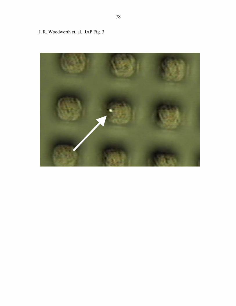
78
J. R. Woodworth et. al. JAP Fig. 3

79
Figure 4; J. R. Woodworth et. al. JAP

80
Fig. 5. J. R. Woodworth et. al. JAP

81
Figu
re 6
, J. R
. Woo
dwor
th e
t. al
. JA
P

82
0
2
4
6
8
10
12
14
16
18
20
0 10 20 30 40 50 60Distance from wall ( microns )
Perc
ent T
rans
mis
sion 23 mTorr, 100 W no bias
23 mTorr, 250 W no bias
23 mTorr, 380 W no bias
hole fluxes summary.xls 4
Fig. 7, J. R. Woodworth et. al. JAP

83
0
5
10
15
20
25
30
0 10 20 30 40 50 60distance from wall ( microns )
Perc
ent T
rans
mis
sion
23 mTorr, 100 W, with bias
23 mTorr, 250 W, with bias
23 mTorr, 380 W, with bias
hole fluxes sum mary.xls5
Fig. 8, J. R. Woodworth et. al. JAP

84
0
5
10
15
20
25
30
35
0 10 20 30 40average ion energy ( eV )
Perc
ent T
rans
mis
sion
5 mTorr, 250 W
23 mTorr, 250 W
23 mTorr, 380 W
iad corner summary.xls
Fig. 9, J. R. Woodworth et. al. JAP

85
-0.06
-0.04
-0.02
0
0.02
0.04
0.06
0.08
0.1
0 10 20 30 40 50ion energy ( eV )
ion
Flux
ied121300d.xls
on flat / 10
center of hole
11 um from wall
Figure 10, J. R. Woodworth et. al. JAP

86
-0.2
-0.15
-0.1
-0.05
0
0.05
0.1
0.15
0.2
0.25
0 10 20 30 40 50 60Ion energy ( eV )
ion
Flux
ied11400zr.xls
on Flat / 2
center of hole
11 um from wall
18.5 um from wall
Figure 11, J. R. Woodworth et. al. JAP

87
S1S2S3S4S5S6S7S8S9S10S11S12S13S14S15S16S17S18S19S20S21S22S23S24S25S26S27
0.115-0.14
0.09-0.115
0.065-0.09
0.04-0.065
0.015-0.04
-0.01-0.015
iad121400b.xls 6
Centered
(50 um from wall ) 11 um from wall
4 um from wall
iad121400b.pptFig. 12, J. R. Woodworth et. al. JAP
18.5 um fromwall
Ion Flux

88
1 3 5 7 9 11 13 15 17 19 21 23 25 27
S1S2S3S4S5S6S7S8S9S10S11S12S13S14S15S16S17S18S19S20S21S22S23S24S25S26S27
i o n F l u x
0.4-0.5
0.3-0.4
0.2-0.3
0.1-0.2
0-0.1
Centered
18 um fromwall
11 um from wall
4 um from wall
Ion Flux
Fig. 13, J. R. Woodworth et. al. JAP

89
Centered
S1S2S3S4S5S6S7S8S9S10S11S12S13S14S15S16S17S18S19S20S21S22S23S24S25S26S27
0.75-0.90.6-0.750.45-0.60.3-0.450.15-0.30-0.15
18 um from wall
11 um from wall
4 um from wall
Hole 23 micronbiased data.ppt
Fig. 14, J. R. Woodworth et. al. JAP
Ion Flux

90
-0.05
0.15
0.35
0.55
0.75
-0.05
0.15
0.35
0.55
0.75
0.95
A: Ion Angular Distributionin center of 100 micron hole
B: Ion Angular distributionnear wall of 100 micron hole
Figure 15 J. R. Woodworth et. al. JAP23 mTorr, 250 W with rf bias

91
+ +
B: sheath muchlarger than 100microns
A: sheathcomparable to100 microns
100-micronsquare holes
Fig 16 J. R. Woodworth et. al. JAP
Equipotentiallines
92
References
1 E. Kawamura, V. Vahedi, M. A. Lieberman and C. K. Birdsall, Plasma Sources Sci.
Technol. 8(1999) R45-R64
2 M. A. Sobolewski, Phys. Rev. E 62(p8540) 2000
3 D. Bose, T. R. Govindan, and M. Meyyappan, JAP 87,(10) May 2000, p. 7176
4 E. A. Edelberg and E. S. Aydil, JAP, 86(9) Nov. 1999, p.4799
5 P. A. Miller and M. E. Riley, JAP 82(8)Oct. 1997 p.3689
6 J. Hoekstra, M. Grapperhaus, and M. J. Kushner, J. Vac. Sci. Technol A 15 1913 (1997)
7 E. Meeks, P. Ho, A. Tingand, R. Buss, J. Vac. Sci. Technol A 16 2227 (1998)
8 J. Johannes, T. Bartel, G. Hebner, J. Woodworth, and D. Economou, J. Electrochem.
Soc. 144 (7) p.2448 July 1997
9 A. N. Goyette, Y. Wang, M. Misakian, and J. K. Olthoff, J. Vac. Sci Technol. A 18(6)
2785 (2000)
10 C. A. Nichols, J. R. Woodworth and T. W. Hamilton J. Vac. Sci. Technol. A 16(6)
3389 ( 1998)
11 U. Kortshagen and M. Zethoff, Plasma Sources Sci, Technol. 4, 541, (1995)
12 J. R. Woodworth, M. E. Riley, P. A. Miller, C. A. Nichols, T. W. Hamilton, J. Vac.
Sci. Technol. A 15(6) 3015 (1997)
13 J. Hopwood, Appl. Phys Lett. 62, 940 (1993)
14 E. S. Aydil, B. O. M. Quiniou, J. T. C. Lee, J. A. Gregus, R. A. Gottscho, Materials
Sci. in Semiconductor processing 1, p. 75, (1998) Pergammon Press, London
15 K. Kohler, J. W. Coburn, D. E. Horne, E. Kay, J. H. Keller J. Appl. Phys. 57(1) p.59-
66 (1985)

93
16 J. Hopwood, Appl. Phys. Lett. 62 (9) p.940 (1993)
17 M. G. Blain, J. E. Stevens, J. R. Woodworth, and C. E. Nichols, Proceedings of the 9th
Conference on Plasma Dynamics and Lasers, Albuquerque, NM June 1998, Americal
Institute of Aeronautics and Astronautics.
18 J. Janes, J. Vac. Sci. Technol. A 12 (1), 97 (1994)
19 A. D. Kupyers and H. J. Hopman, J. Appl. Phys. 67 (3), p1229, (1990)
20 F. Becker, I. W. Rangelow, R.Kassing, J. Appl. Phys 89 (1) p. 56 (1996)
21 M. Zeuner, H. Neumann, J. Appl. Phys. 81(7), p. 2985, (1997)
22 A. Mannenschijn, E van der Drift, G. C. A. M. Janssen, S. Radelaar, J. Appl. Phys.
69(1) p. 7996, (1991)
23 P. K. Loewenhardt, H. Hanawa, D. X. Ma, P. Salzman, K. Chuc, A. Sato, V. Todorov,
and G. Z. Yin, Proc, Electrochem. Soc. 96, 234 (1996)
24 J. Trow, Bulletin of the American Physical Society, 39 (6) p. 1488, (1994)
25 Y. Hikosaka, H. Hayashi, M Sekine, H Tsuboi, M Endo, N. Mizutani, Jpn. J. Appl
Phys, 38, 4465 (1999) 26 N. Mizutani and T. Hayashi, J. Vac. Sci. Technol. A 19(4), 1298, (2001). 27 E. A. Edelberg, A. Perry, N. Benjamin, and E. S. Aydil, JVSTA 17(2) Mar. 1999, p.
506
28 A. Metze, D. W. Ernie, and H. J. Oskam, JAP 60(9), Nov. 1986, p. 308
29 J. R. Woodworth, I. C. Abraham, M. E. Riley, R. A. Miller, T. W. Hamilton, B. P.
Aragon, R. J. Shul, C. G. Willison, Submitted to JVSTA. 30 I. C. Abraham, J. R. Woodworth, M. E. Riley, P. A. Miller, T. W. Hamilton, B. P.
Aragon, Submitted to JVSTA 31 P. J. Hargis et. al. Rev. Sci. Inst. 65 (1994) p. 140

94
32 P. A. Miller et. al. Journal of Research of the National Institute of Standards and
Technology, 100(4), July 1995, p. 427
33 R. J. Shul and S. J Pearton “Handbook of Advanced Plasma Processing Techniques”,
Springer, Berlin, 2000, ISBN 3-540-66772-5, p. 148
34 V. A. Godyak, R. B. Piejak B. M. Alexandrovitch, Plasma Sources Sci. Technol. 1, 36-
58 (1992)
35 D. N. Ruzic, Electric Probes for Low Temperature Plasmas, AVS monograph M-13, (
American Vacuum Society Press, New York, 1994)
36 R. J. Shul and S. J. Pearton IBID, p. 162
37 N. Benjamin, Rev. Sci. Instrum. 53, 1541, (1982)
38 V. A. Godyak, R. B. Piejak, and B. M. Alexandrovich, J. App. Phys. 85 (2) p.703, 15
January 1999
39 J. R. Woodworth, B. P. Aragon, T. W. Hamilton, Appl. Phys. Lett 70 (15) p. 1947,
(1997)
40 National Aperture, 26 Keewaydin Drive, Salem, New Hampshire, 03079, (603) 893-
7393
41 J. R. Woodworth, M. E. Riley, D. C. Meister, B. P. Aragon, M. S. Le, H. H. Sawin, J.
Appl. Phys 80 1304 (1996)
42 Unique Wire Weaving Co. Inc. 762 Ramsey Ave. Hillside N.J. 07205
43 J. R. Woodworth, M. E. Riley, G. A. Hebner, T. W. Hamilton, J. Appl. Phys. 81 (9)
1997, p. 5950 44 K & L microwave Inc. 22540 Northwood Dr. Salisbury Md, 21801
45 J. R. Woodworth, P. A. Miller, R. J. Shul, I. C. Abraham, B. P. Hamilton, C. G.

95
Willison, D. Economou, D. Kim, “ Ions near steps – A theoretical and experimental
study of Ion Distributions near surface features on rf-biased wafers in plasma etching
discharges.” Submitted to JVSTA

96
DISTRIBUTION:
20 MS 1423 G. A. Hebner, 01118 2 MS 1423 J. R Woodworth, 01645 1 MS 0886 I. C. Abraham, 01812 2 MS 1423 G. N. Hays, 01118 1 MS 9018 Central Technical Files, 8945-1 2 MS 0899 Technical Library, 9616 1 MS 0612 Review & Approval Desk, 9612 [For DOE/OSTI] 1 MS 1380 Technology Transfer