Embed Size (px)
Citation preview
CHARACTERIZING THE AGING-DRIVEN DEGRADATION RATE OF ELECTRICAL
CONTACT RESISTANCE AND MECHANICAL INTEGRITY OF PLASTIC-ENCAPSULATED
AU/AL WIRE BONDS
A Dissertation Submitted to the Graduate Faculty
of the North Dakota State University
of Agriculture and Applied Science
By
Syed Sajid Ahmad
In Partial Fulfillment of the Requirements for the Degree of
DOCTOR OF PHILOSOPHY
Major Program: Engineering
December 2019
Fargo, North Dakota

ii
North Dakota State University Graduate School
Title
CHARACTERIZING THE AGING-DRIVEN DEGRADATION RATE OF
ELECTRICAL CONTACT RESISTANCE AND MECHANICAL INTEGRITY
OF PLASTIC-ENCAPSULATED AU/AL WIRE BONDS
By
Syed Sajid Ahmad
The Supervisory Committee certifies that this disquisition complies with North
Dakota State University’s regulations and meets the accepted standards for the
degree of
DOCTOR OF PHILOSOPHY
SUPERVISORY COMMITTEE:
Scott Smith
Chair
Xinnan Wang
Qifeng Zhang
Danling Wang
Approved: 12/16/19 Ben Braaten Date Department Chair
iii
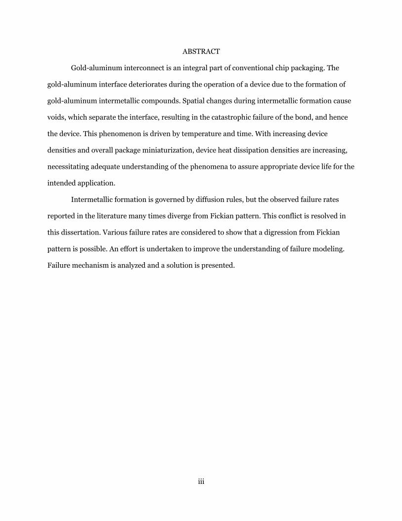
ABSTRACT
Gold-aluminum interconnect is an integral part of conventional chip packaging. The
gold-aluminum interface deteriorates during the operation of a device due to the formation of
gold-aluminum intermetallic compounds. Spatial changes during intermetallic formation cause
voids, which separate the interface, resulting in the catastrophic failure of the bond, and hence
the device. This phenomenon is driven by temperature and time. With increasing device
densities and overall package miniaturization, device heat dissipation densities are increasing,
necessitating adequate understanding of the phenomena to assure appropriate device life for the
intended application.
Intermetallic formation is governed by diffusion rules, but the observed failure rates
reported in the literature many times diverge from Fickian pattern. This conflict is resolved in
this dissertation. Various failure rates are considered to show that a digression from Fickian
pattern is possible. An effort is undertaken to improve the understanding of failure modeling.
Failure mechanism is analyzed and a solution is presented.
iv
ACKNOWLEDGEMENTS
I first studied the phenomenon of Au-Al interactions while at Intel under the supervision
of Dr. Richard Blish II in the late 70s and early 80s. This was the period of moving electronic
components from ceramic to plastic packaging necessitating the introduction of gold wire
bonding. The mechanics of the Au-Al interconnect continued to intrigue me as I moved through
my career in industry and dealt with the problem almost on a daily basis. After joining NDSU, as
I tried to increase my understanding of the Au-Al interface, Dr. Blish was again at hand to help
me in gathering, organizing and comprehending the history of the studies on Au-Al interface
and analyzing various scientific aspects. Dr. Blish played a major role in my curiosity and its
methodical study over so many years.
The initial supervisory committee members at NDSU, Dr. You, Dr. Wells, Dr. Shi and Dr.
Kong provided me with an impetus to continually pursue the issue until I reached the solution
presented here.
At NDSU, help of Dr. Scott Smith was critical in continuing my quest and bringing it to
fruition. He reviewed numerous versions of the work through the process of getting the results
published.
Dr Glen Shirley reviewed the narrative and provided critical additions and deletions. My
resultant IEEE Transactions paper greatly benefitted from his review and analysis of the models,
and his advice.
A summarized version of this disquisition has been published in IEEE Transactions on
Device and Materials Reliability. IEEE reviewers helped in streamlining the study and in the
succinct narration of the results.
With the help and support of the members of the current supervisory committee, Dr.
Smith, Dr. Xinnan Wang, Dr. Zhang and Dr. Danling Wang, I am able to submit my final
disquisition.

v
DEDICATION
Dedicated to my parents, Syed Sajjad Haider and Syeda Riaz Fatima,
for imprinting the value of education and inquisitiveness in me from my childhood,
to my wife, Syeda Bushra Sultana Ahmad,
for her persistent encouragement and support in writing this manuscript,
and to my children, Aamra, Aisha, Yusuf and Samra.

vi
PREFACE
Au-Al intermetallic formation and degradation is a diffusion driven phenomenon. While
studying the effect of bromine in molding compounds on the degradation rates of Au-Al bonds,
it was observed that the change in bond resistance caused by the progression of intermetallic
compounds did not follow the expected pattern dictated by diffusion science [1]. The anomaly
intrigued my interest and I continued to research the matter to reach the solution presented in
this dissertation.
vii
TABLE OF CONTENTS
ABSTRACT ..................................................................................................................................... iii
ACKNOWLEDGEMENTS .............................................................................................................. iv
DEDICATION ..................................................................................................................................v
PREFACE ....................................................................................................................................... vi
LIST OF TABLES ........................................................................................................................... ix
LIST OF FIGURES ...........................................................................................................................x
LIST OF ABBREVIATIONS .......................................................................................................... xii
LIST OF SYMBOLS ...................................................................................................................... xiii
1. INTRODUCTION ......................................................................................................................... 1
2. MEASUREMENT OF AU-AL BOND INTERFACE INTEGRITY ............................................... 2
3. LITERATURE REVIEW .............................................................................................................. 9
3.1. Bond Electrical Resistance as a Measure of Au-Al Bond Interface Integrity ....................... 9
3.2. Previous Studies Showing Digression of Resistance Change Pattern from Fickian Behavior ............................................................................................................................. 13
4. PROBLEM DEFINITION ......................................................................................................... 28
5. RESOLUTION TO THE PROBLEM OF RECONCILIATION OF NON-COMPLIANT DATA IN REGARDS TO THE APPLICATION OF THE T½ LAW TO AU-AL WIRE BOND DEGRADATION ........................................................................................................... 30
6. EVIDENCE AND SIMULATIONS TO RESOLVE THE NON-COMPLIANCE ISSUE ............. 32
6.1. Constant Rate of Void Formation ...................................................................................... 37
6.2. Decreasing Rate of Void Formation .................................................................................. 37
6.3. Increasing Rate of Void Formation ................................................................................... 37
6.4. Equivalence of the Three Models ...................................................................................... 40
6.5. Summary of Rates of Void Formation ............................................................................... 43
6.6. Case of Circular Initiation and Progression of Intermetallic Compounds in the Au-Al Interfacial Disc .................................................................................................................. 43
7. CONCLUSIONS AND FUTURE WORK ................................................................................... 44

viii
REFERENCES .............................................................................................................................. 45
ix
LIST OF TABLES
Table Page
I. Various rates of diffusion found in literature ......................................................................... 28
II. Specific Resistances of intermetallic phases [2] .................................................................... 32
III. Three models of conductive (non-voided) bond area as a function of age............................. 39
x
LIST OF FIGURES
Figure Page
1. Wire pull method to test the condition of a wire bond ............................................................. 2
2. Wire pull failure modes ............................................................................................................ 3
3. Ball shear testing method for Au-Al interface integrity ........................................................... 4
4. Ball bond failure modes ............................................................................................................. 5
5. A cross section of a gold-aluminum interface (left) and identification of different intermetallic phases (right) [4]. ................................................................................................ 6
6. Intermetallic proliferation observed through IR [4]. ............................................................... 6
7. Silicon precipitates and probe marks observed using IR [4]..................................................... 7
8. Gold ball bond resistance ........................................................................................................... 7
9. Resistance measurement arrangements for control and test structures. ................................. 8
10. Time to failure versus reciprocal absolute temperature for bonds made to aluminum films of different thicknesses. Open points are for electrical failures, darkened points are for mechanical failures, and half darkened points are for samples that exhibited both failure modes [11]. .................................................................................................................... 10
11. Pad area increase with ball size. .............................................................................................. 11
12. Bond area ratio to wire sectional area. .................................................................................... 12
13. Mean Resistance as a Function of Storage Time [17] .............................................................. 13
14. Changes in electrical resistance of evaporated bimetal films of aluminum and gold subjected to successive heat treatment in vacuo [15]. ............................................................. 14
15. Bond resistance as a function of storage temperature (average values) … bond of 36-60 bond lops in series [3]. ............................................................................................................. 15
16. Oswald’s 1975 graph restructured to show the threshold temperature [3]. ............................ 15
17. Schematized graph of contact resistance change for the different test group, with scales chosen to show the observations at 200°C [18]....................................................................... 16
18. (a) Resistance increase at 200°C. Flame retardant compound X; (b) Resistance increase at 200°C. Flame retardant compound Y; (c) Resistance increase at 175°C. Flame retardant compound X; (d) Resistance increase at 175°C. Flame retardant compound Y [1]. ............................................................................................................................................ 17

xi
19. Mean resistance versus square root of time: for each data point, the resistance of twelve bonds on the same sample was compared to the mean of the unannealed metallization type [19]. .................................................................................................................................. 18
20 Arrhenious plot of thermal aging data [21]. ............................................................................. 19
21. Change of the resistivity of bonds during annealing in N2 (275°C) or in argon (10-2 mbar) at various temperatures [22]. ................................................................................................. 20
22. Morphology of the degradation mechanism (schematic) [22]. .............................................. 20
23. Shear force and change of resistivity as a function of time for a series of bonds annealed at 300°C in N2. [22] ................................................................................................................. 21
24. Micrographs of fracture faces after the shear test. Type 1: no annealing; type 2: short annealing; type 3; extended annealing [22]. .......................................................................... 22
25. (a) Micrograph of the bottom of a bond after 70 h annealing at 300°C in N2. (b) Ring of intermetallic compound when separated from the bottom of a bond after fracture [22]. ..... 23
26. Electrical resistance measured at room temperature as a function of annealing time for various temperatures for the Au/Al system (1) and the Au/Al2O3/Al system (2) [23]. .......... 24
27. Relationship between resistivity and annealing temperature [23]. ........................................25
28. Tsuge 1995 graphs repositioned to align the x-axisscales for data comparison. [23] ............ 26
29. Au-Al interconnect resistance data [24]. ................................................................................. 27
30. Au-Al contact area of the interface disk decreases with time-temperature progression. ....... 31
31. Intermetallic growth with voids [34]. ..................................................................................... 33
32. Au-Al interface ........................................................................................................................ 34
33. Resistance change as voids proliferate ................................................................................... 38
34. Resistance change (logarithmic scale) .................................................................................... 38
35. Plots of Area vs Age (left) and Resistance (reciprocal of Area) vs Age for each of the three models of bond area reduction rate given in Table III. .......................................................... 40
36. Resistance Change (early trend) ............................................................................................. 42
37. Resistance change (end of life trend) ..................................................................................... 42
xii
LIST OF ABBREVIATIONS
eV .......................................................electron Volt
IMC ....................................................intermetallic compound, a stoichiometric combination of two or more metals, possessing with very different mechanical an electrical properties than any of the pure metal components
IR........................................................infra-red
xiii
LIST OF SYMBOLS
ΔR.......................................................resistance change
R .........................................................resistance
ρ .........................................................specific resistance

1
1. INTRODUCTION
Use of aluminum metal for on-chip interconnect in semiconductor devices is a widely
used and mature process. The aluminum terminals on the chip are routed to the chip housing
(package) with gold wires making Au-Al bonds. These bonds degrade over time. The
degradation is caused by the diffusion of gold and aluminum at the joining interface, and is
mainly heat driven.
The diffusion at the interface of two metals follows square-root progression over time.
Previous work on the degradation of Au-Al bonds shows that the electrical resistance of the
gold-aluminum interface many times digresses from the Fickian pattern, and degrades with
time in other patterns, including exponential progression. This dissertation addresses this
incongruence and a presents a solution.
The previous work published on the topic of Au-Al bond lifetimes covers experiments to
show degradation. This dissertation is an attempt to explain the physical basis for the
phenomenon, which can lead to the understanding of the reported failure rate patterns for the
life of the gold-aluminum bonds. An effort to explore the fitness of the available data to a
proposed solution has the possibility of leading to a study useful in mathematical prediction of
the lifetimes for such interconnects and systems.
This dissertation comprises compilation of the history of experimental work and
resulting data and conclusions to-date, and its analysis against empirical relationship and
proposed solution. The literature is surveyed and the proposed hypotheses to date are
summarized. The literature is also surveyed to examine the physical data presented to date and
the empirical degradation rate indicated by the respective data.
A solution is proposed that adequately explains the degradation mechanism. The
solution shows that the resistance change patterns may deviate from Fickian predictions. The
solution presented helps in resolving the incongruence observed experimentally and reported in
previous studies of the Au-Al interface degradation.

2
2. MEASUREMENT OF AU-AL BOND INTERFACE INTEGRITY
In the semiconductor packaging studies and evaluations, the quality, integrity, health,
and degradation of the Au-Al bond is measured in a number of ways.
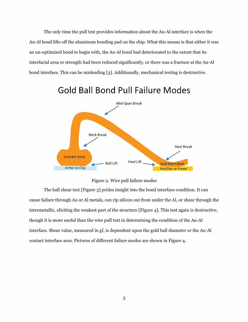
Mechanically, it is measured by pulling the wire or by shearing the Au-Al joint [Figure 1].
The results of the wire pull test are given in the form of the pull strength in gram-force (gf) and
the corresponding failure modes [Figure 2].
Figure 1. Wire pull method to test the condition of a wire bond
In a wire pull test, when the wire fails in the mid-span, the only thing the pull test tells is
that the gold ball bond to the aluminum bonding pad on the chip and to the bonding pad on the
substrate or lead frame is stronger than the wire itself. As-made unstressed bonds made using
an optimized ball bonding process are expected to fail at wire mid-span as the gold ball bond
area to the bonding pad on the chip is two to ten times larger than the cross sectional area of the
wire itself. Failure at other locations may only occur if the process is not set up properly.
If the failure is at the neck of the ball bond to the pad on the chip or at the neck of the
stitch bond to the substrate or lead frame, again it does not provide much insight into the
condition of the Au-Al bond, and just indicates weakness at the neck of the ball bond or at the
neck of the stitch bond. Reasons for such failures have been studied extensively over the years
[2].
3
The only time the pull test provides information about the Au-Al interface is when the
Au-Al bond lifts off the aluminum bonding pad on the chip. What this means is that either it was
an un-optimized bond to begin with, the Au-Al bond had deteriorated to the extent that its
interfacial area or strength had been reduced significantly, or there was a fracture at the Au-Al
bond interface. This can be misleading [3]. Additionally, mechanical testing is destructive.
Figure 2. Wire pull failure modes
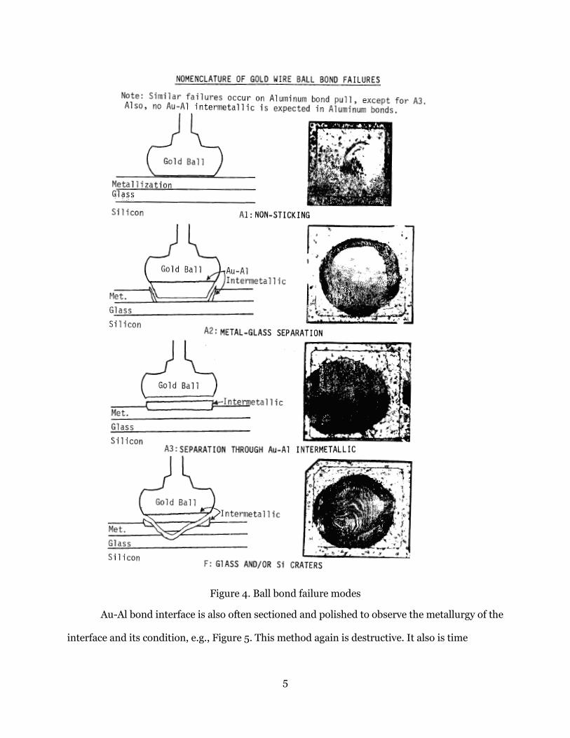
The ball shear test [Figure 3] prides insight into the bond interface condition. It can
cause failure through Au or Al metals, can rip silicon out from under the Al, or shear through the
intermetallic, eliciting the weakest part of the structure [Figure 4]. This test again is destructive,
though it is more useful than the wire pull test in determining the condition of the Au-Al
interface. Shear value, measured in gf, is dependent upon the gold ball diameter or the Au-Al
contact interface area. Pictures of different failure modes are shown in Figure 4.

4
Figure 3. Ball shear testing method for Au-Al interface integrity
5
Figure 4. Ball bond failure modes
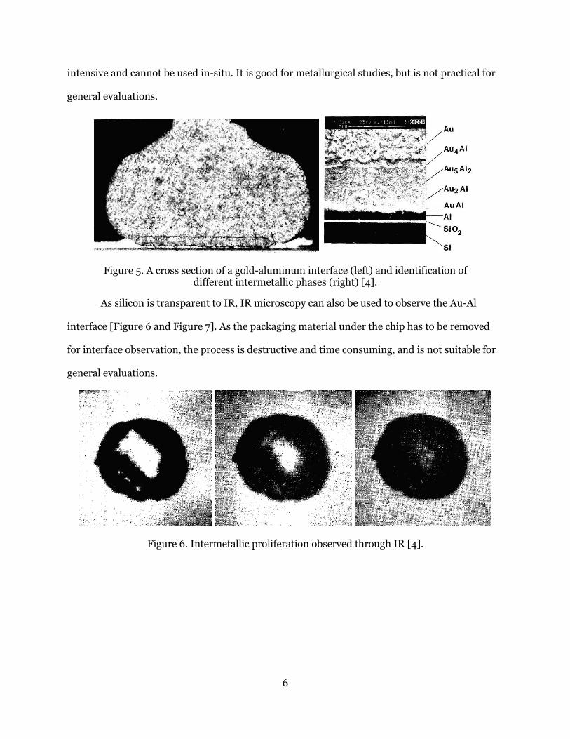
Au-Al bond interface is also often sectioned and polished to observe the metallurgy of the
interface and its condition, e.g., Figure 5. This method again is destructive. It also is time
6
intensive and cannot be used in-situ. It is good for metallurgical studies, but is not practical for
general evaluations.
Figure 5. A cross section of a gold-aluminum interface (left) and identification of different intermetallic phases (right) [4].
As silicon is transparent to IR, IR microscopy can also be used to observe the Au-Al
interface [Figure 6 and Figure 7]. As the packaging material under the chip has to be removed
for interface observation, the process is destructive and time consuming, and is not suitable for
general evaluations.
Figure 6. Intermetallic proliferation observed through IR [4].
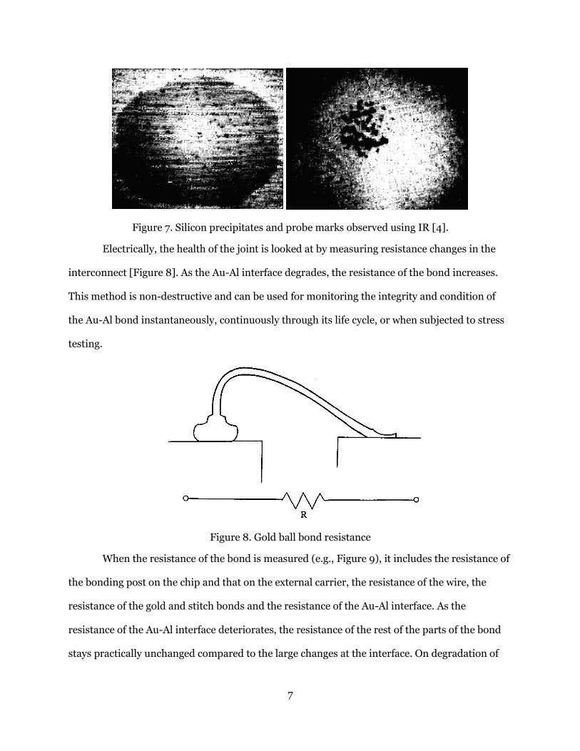
7
Figure 7. Silicon precipitates and probe marks observed using IR [4].
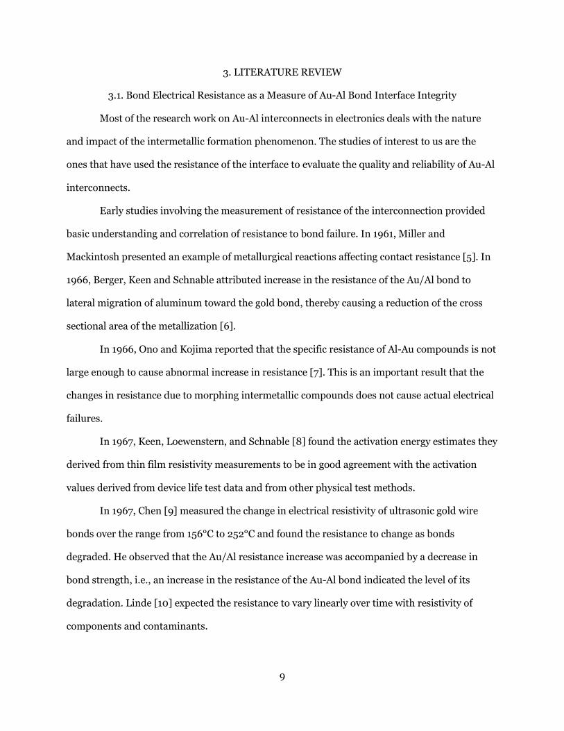
Electrically, the health of the joint is looked at by measuring resistance changes in the
interconnect [Figure 8]. As the Au-Al interface degrades, the resistance of the bond increases.
This method is non-destructive and can be used for monitoring the integrity and condition of
the Au-Al bond instantaneously, continuously through its life cycle, or when subjected to stress
testing.
Figure 8. Gold ball bond resistance
When the resistance of the bond is measured (e.g., Figure 9), it includes the resistance of
the bonding post on the chip and that on the external carrier, the resistance of the wire, the
resistance of the gold and stitch bonds and the resistance of the Au-Al interface. As the
resistance of the Au-Al interface deteriorates, the resistance of the rest of the parts of the bond
stays practically unchanged compared to the large changes at the interface. On degradation of

8
the interface, the resistance at first “changes” very minutely while the intermetallic compounds
are formed. Larger changes to resistance start taking place when Kirkendall voids start showing
up. These changes accelerate in the presence of halides.
Figure 9. Resistance measurement arrangements for control and test structures.
As resistance provides the opportunity for continuous and in-situ measurement of the
condition of the Au-Al interface, it is the favored choice for the evaluation of the quality and
reliability of Au-Al bonds. This method has been used by researchers for decades due to its
efficiency and effectiveness.
9
3. LITERATURE REVIEW
3.1. Bond Electrical Resistance as a Measure of Au-Al Bond Interface Integrity
Most of the research work on Au-Al interconnects in electronics deals with the nature
and impact of the intermetallic formation phenomenon. The studies of interest to us are the
ones that have used the resistance of the interface to evaluate the quality and reliability of Au-Al
interconnects.
Early studies involving the measurement of resistance of the interconnection provided
basic understanding and correlation of resistance to bond failure. In 1961, Miller and
Mackintosh presented an example of metallurgical reactions affecting contact resistance [5]. In
1966, Berger, Keen and Schnable attributed increase in the resistance of the Au/Al bond to
lateral migration of aluminum toward the gold bond, thereby causing a reduction of the cross
sectional area of the metallization [6].
In 1966, Ono and Kojima reported that the specific resistance of Al-Au compounds is not
large enough to cause abnormal increase in resistance [7]. This is an important result that the
changes in resistance due to morphing intermetallic compounds does not cause actual electrical
failures.
In 1967, Keen, Loewenstern, and Schnable [8] found the activation energy estimates they
derived from thin film resistivity measurements to be in good agreement with the activation
values derived from device life test data and from other physical test methods.
In 1967, Chen [9] measured the change in electrical resistivity of ultrasonic gold wire
bonds over the range from 156°C to 252°C and found the resistance to change as bonds
degraded. He observed that the Au/Al resistance increase was accompanied by a decrease in
bond strength, i.e., an increase in the resistance of the Au-Al bond indicated the level of its
degradation. Linde [10] expected the resistance to vary linearly over time with resistivity of
components and contaminants.

10
In 1969, Anderson compared the times for electrical and mechanical failures [11]. The
data [Figure 10] shows the time to failure observed for aging temperatures of 125, 200, 300, and
400°C. They used a median value of greater than 1 ohm for electrical failures compared to initial
resistance of 0.1 ohm.
Figure 10. Time to failure versus reciprocal absolute temperature for bonds made to aluminum films of different thicknesses. Open points are for electrical failures, darkened points are for mechanical failures, and half darkened points are for
samples that exhibited both failure modes [11].

11
The data shows that electrical failures occur before the mechanical failures, eliciting the
role of voids in reducing the cross-sectional area of the bond.
Initially, as the gold ball is larger than the wire diameter, the cross-sectional gold-to-
aluminum bond area is much larger than the cross-sectional area of the gold wire itself. As
degradation at the gold-aluminum interface reduces the contact area, failure will continue to
take place in the wire until the Au-Al contact area is reduced sufficiently to become weaker than
the wire itself.
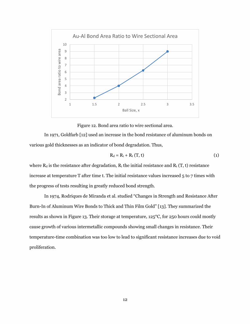
Figure 11. Pad area increase with ball size.
As shown in Figure 11 and Figure 12, the Au-Al contact area is much larger than the gold
wire sectional area; therefore, wire pull testing can show a failure at the gold-aluminum
interface only after a large reduction in the Au-Al interface area.
0
1000
2000
3000
4000
5000
6000
7000
1 1.5 2 2.5 3 3.5
Bond
Are
a, µ
m2
Ball Size (Wire Diameter x)
Ball Bond Area Multiplies with Ball Size Increase
20 micron wire
25 micron wire
30 micron wire
12
Figure 12. Bond area ratio to wire sectional area.
In 1971, Goldfarb [12] used an increase in the bond resistance of aluminum bonds on
various gold thicknesses as an indicator of bond degradation. Thus,
Rd = Ri + Rt (T, t) (1)
where Rd is the resistance after degradation, Ri the initial resistance and Rt (T, t) resistance
increase at temperature T after time t. The initial resistance values increased 5 to 7 times with
the progress of tests resulting in greatly reduced bond strength.
In 1974, Rodriques de Miranda et al. studied “Changes in Strength and Resistance After
Burn-In of Aluminum Wire Bonds to Thick and Thin Film Gold” [13]. They summarized the
results as shown in Figure 13. Their storage at temperature, 125°C, for 250 hours could mostly
cause growth of various intermetallic compounds showing small changes in resistance. Their
temperature-time combination was too low to lead to significant resistance increases due to void
proliferation.
2
3
4
5
6
7
8
9
10
1 1.5 2 2.5 3 3.5
Bond
are
a ra
tio to
wire
are
a
Ball Size, x
Au-Al Bond Area Ratio to Wire Sectional Area

13
Figure 13. Mean Resistance as a Function of Storage Time [17]
3.2. Previous Studies Showing Digression of Resistance Change Pattern from Fickian Behavior
Many of the resistance studies explicitly or implicitly have either found the Au-Al bond
degradation to follow a Fickian pattern or to deviate from it. In 1952, Gerritsen and Linde noted
anomalies in the resistance behavior of some noble alloys [14]. In 1960, Belser studied
resistance changes in Au-Al bi-metal films [15] and found that the resistance change did not
follow expected rate of increase over time and temperature [Figure 14].
14
Figure 14. Changes in electrical resistance of evaporated bimetal films of aluminum and gold subjected to successive heat treatment in vacuo [15].
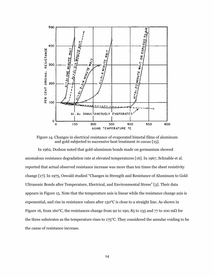
In 1962, Dodson noted that gold-aluminum bonds made on germanium showed
anomalous resistance degradation rate at elevated temperatures [16]. In 1967, Schnable et al.
reported that actual observed resistance increase was more than ten times the sheet resistivity
change [17]. In 1975, Oswald studied “Changes in Strength and Resistance of Aluminum to Gold
Ultrasonic Bonds after Temperature, Electrical, and Environmental Stress” [3]. Their data
appears in Figure 15. Note that the temperature axis is linear while the resistance change axis is
exponential, and rise in resistance values after 150°C is close to a straight line. As shown in
Figure 16, from 160°C, the resistances change from 92 to 190, 85 to 135 and 77 to 100 mΩ for
the three substrates as the temperature rises to 175°C. They considered the annular voiding to be
the cause of resistance increase.

15
Figure 15. Bond resistance as a function of storage temperature (average values) … bond of 36-60 bond lops in series [3].
Figure 16. Oswald’s 1975 graph restructured to show the threshold temperature [3].
16
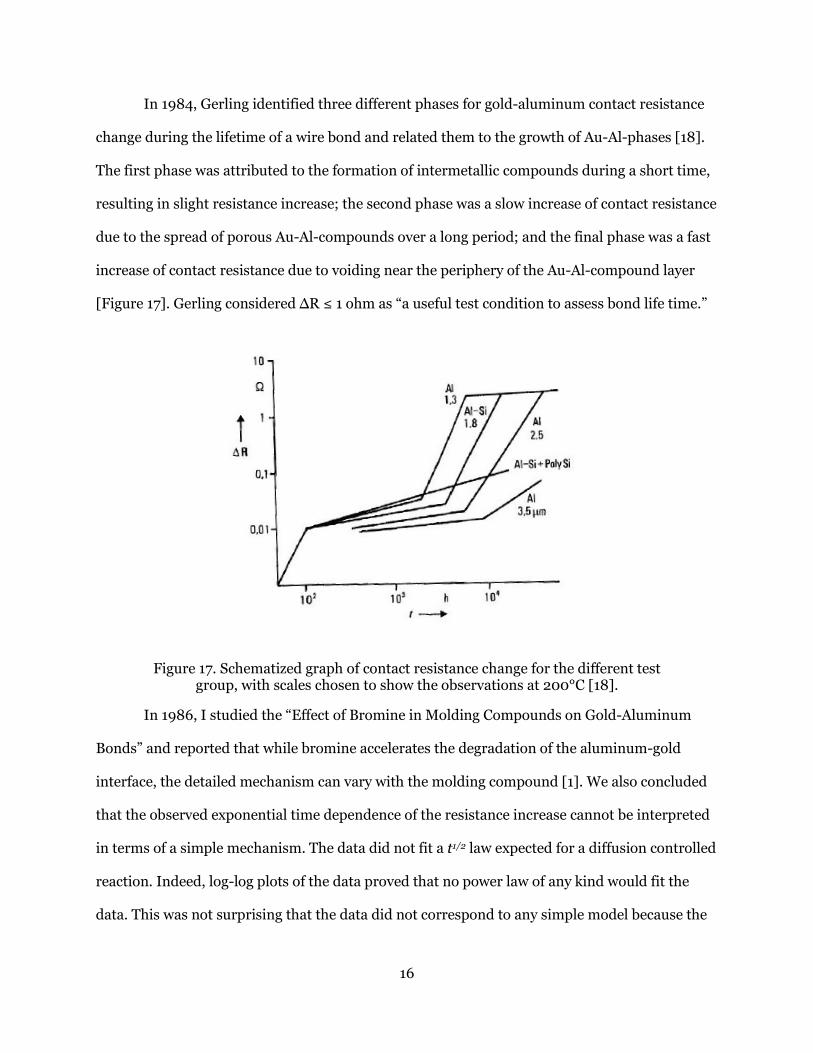
In 1984, Gerling identified three different phases for gold-aluminum contact resistance
change during the lifetime of a wire bond and related them to the growth of Au-Al-phases [18].
The first phase was attributed to the formation of intermetallic compounds during a short time,
resulting in slight resistance increase; the second phase was a slow increase of contact resistance
due to the spread of porous Au-Al-compounds over a long period; and the final phase was a fast
increase of contact resistance due to voiding near the periphery of the Au-Al-compound layer
[Figure 17]. Gerling considered ∆R ≤ 1 ohm as “a useful test condition to assess bond life time.”
Figure 17. Schematized graph of contact resistance change for the different test group, with scales chosen to show the observations at 200°C [18].
In 1986, I studied the “Effect of Bromine in Molding Compounds on Gold-Aluminum
Bonds” and reported that while bromine accelerates the degradation of the aluminum-gold
interface, the detailed mechanism can vary with the molding compound [1]. We also concluded
that the observed exponential time dependence of the resistance increase cannot be interpreted
in terms of a simple mechanism. The data did not fit a t1/2 law expected for a diffusion controlled
reaction. Indeed, log-log plots of the data proved that no power law of any kind would fit the
data. This was not surprising that the data did not correspond to any simple model because the
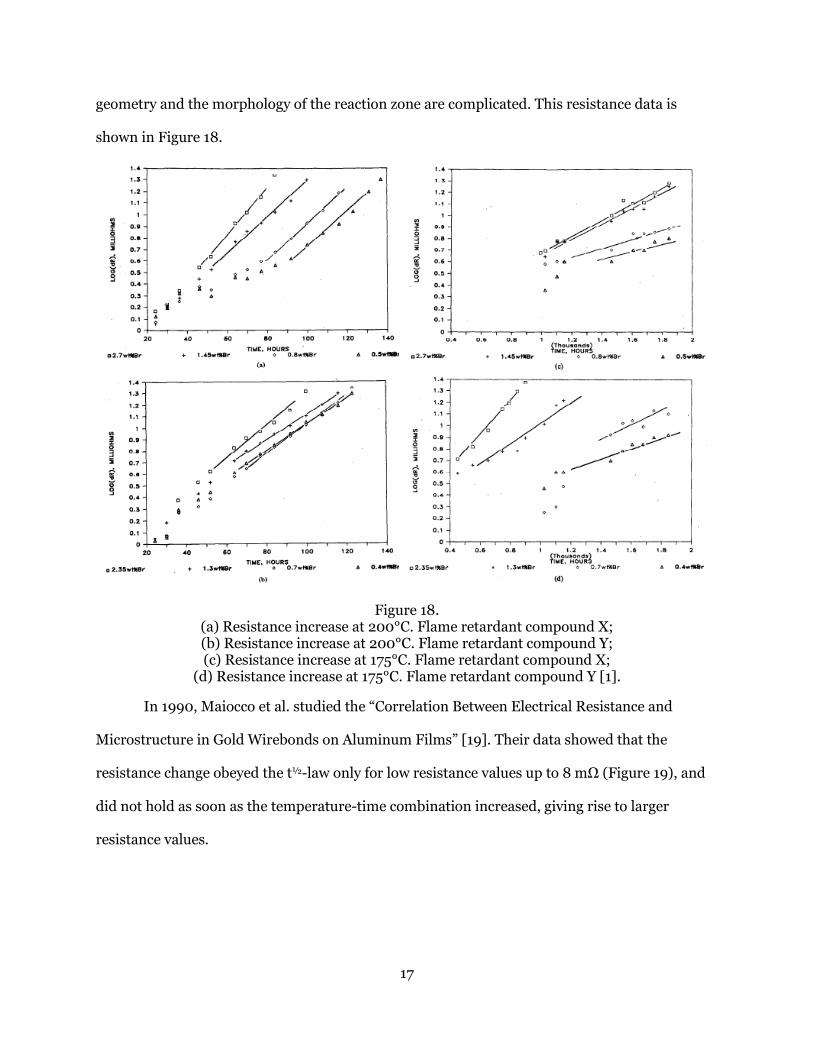
17
geometry and the morphology of the reaction zone are complicated. This resistance data is
shown in Figure 18.
Figure 18. (a) Resistance increase at 200°C. Flame retardant compound X; (b) Resistance increase at 200°C. Flame retardant compound Y; (c) Resistance increase at 175°C. Flame retardant compound X;
(d) Resistance increase at 175°C. Flame retardant compound Y [1].
In 1990, Maiocco et al. studied the “Correlation Between Electrical Resistance and
Microstructure in Gold Wirebonds on Aluminum Films” [19]. Their data showed that the
resistance change obeyed the t½-law only for low resistance values up to 8 mΩ (Figure 19), and
did not hold as soon as the temperature-time combination increased, giving rise to larger
resistance values.
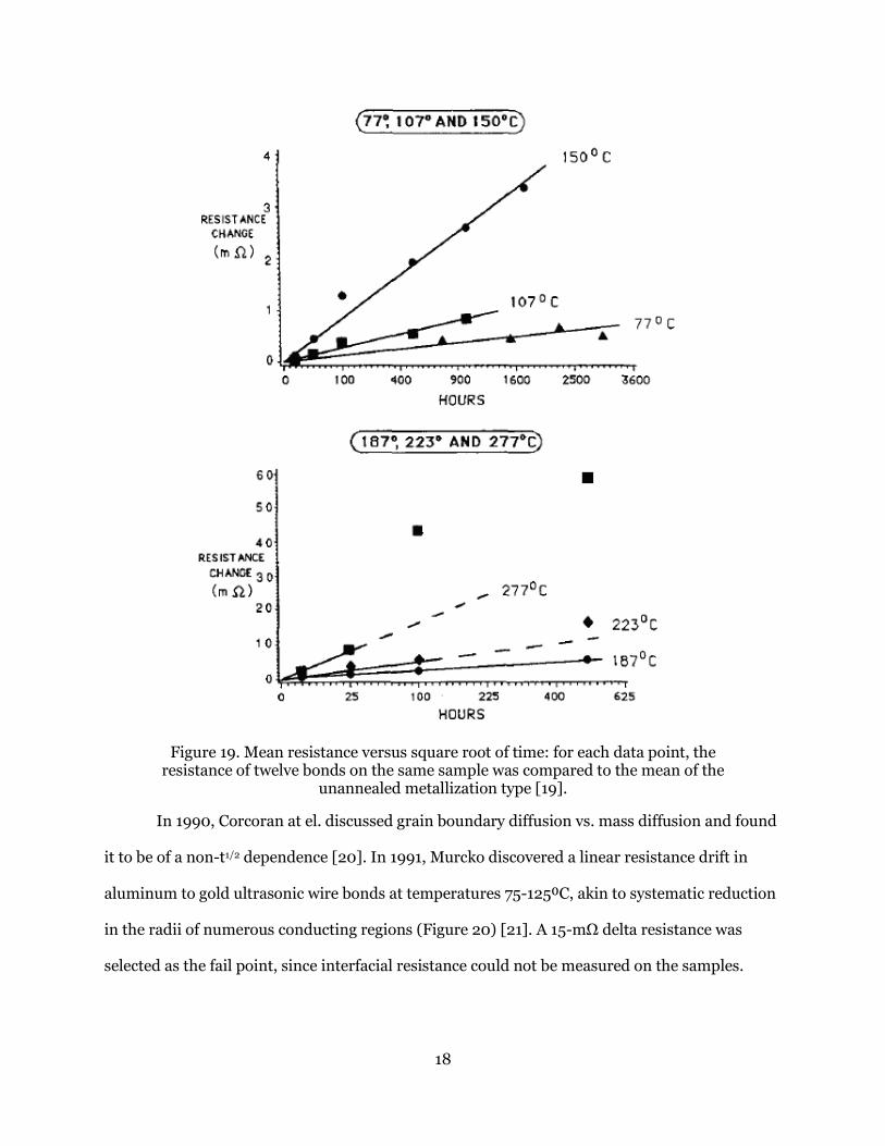
18
Figure 19. Mean resistance versus square root of time: for each data point, the resistance of twelve bonds on the same sample was compared to the mean of the
unannealed metallization type [19].
In 1990, Corcoran at el. discussed grain boundary diffusion vs. mass diffusion and found
it to be of a non-t1/2 dependence [20]. In 1991, Murcko discovered a linear resistance drift in
aluminum to gold ultrasonic wire bonds at temperatures 75-125⁰C, akin to systematic reduction
in the radii of numerous conducting regions (Figure 20) [21]. A 15-mΩ delta resistance was
selected as the fail point, since interfacial resistance could not be measured on the samples.
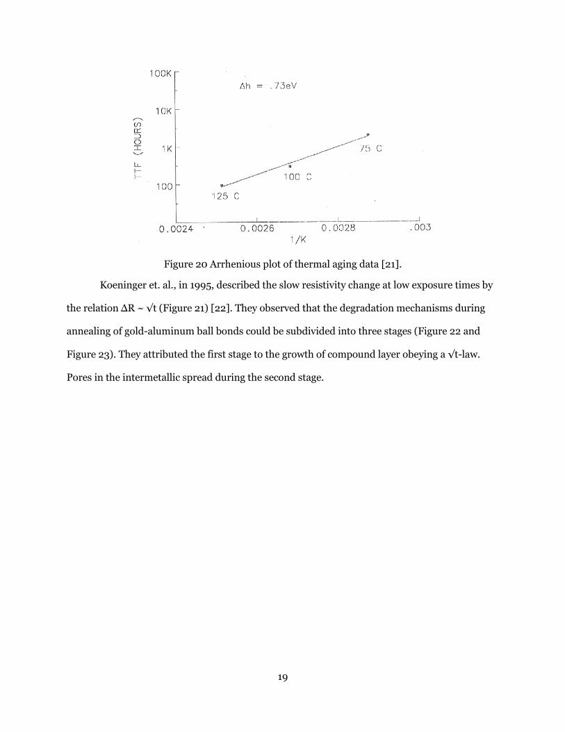
19
Figure 20 Arrhenious plot of thermal aging data [21].
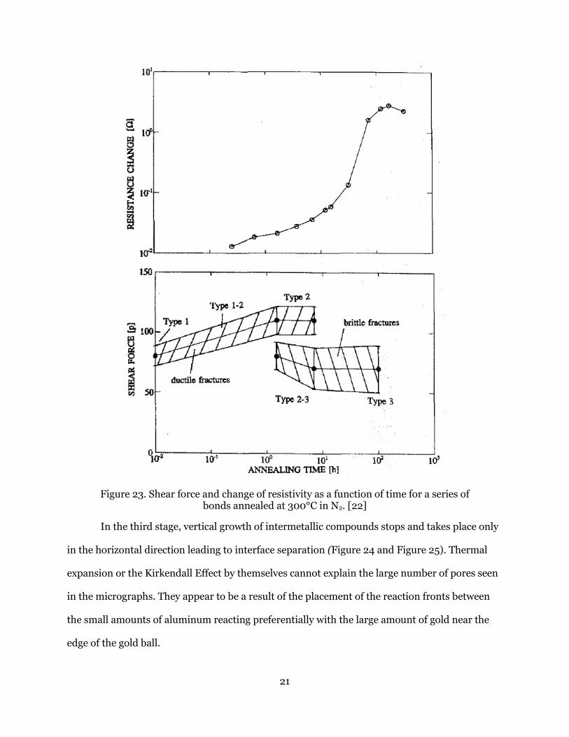
Koeninger et. al., in 1995, described the slow resistivity change at low exposure times by
the relation ΔR ~ √t (Figure 21) [22]. They observed that the degradation mechanisms during
annealing of gold-aluminum ball bonds could be subdivided into three stages (Figure 22 and
Figure 23). They attributed the first stage to the growth of compound layer obeying a √t-law.
Pores in the intermetallic spread during the second stage.

20
Figure 21. Change of the resistivity of bonds during annealing in N2 (275°C) or in argon (10-2 mbar) at various temperatures [22].
Figure 22. Morphology of the degradation mechanism (schematic) [22].
21
Figure 23. Shear force and change of resistivity as a function of time for a series of bonds annealed at 300°C in N2. [22]
In the third stage, vertical growth of intermetallic compounds stops and takes place only
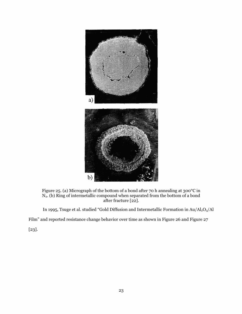
in the horizontal direction leading to interface separation (Figure 24 and Figure 25). Thermal
expansion or the Kirkendall Effect by themselves cannot explain the large number of pores seen
in the micrographs. They appear to be a result of the placement of the reaction fronts between
the small amounts of aluminum reacting preferentially with the large amount of gold near the
edge of the gold ball.

22
Figure 24. Micrographs of fracture faces after the shear test. Type 1: no annealing; type 2: short annealing; type 3; extended annealing [22].
23
Figure 25. (a) Micrograph of the bottom of a bond after 70 h annealing at 300°C in N2. (b) Ring of intermetallic compound when separated from the bottom of a bond
after fracture [22].
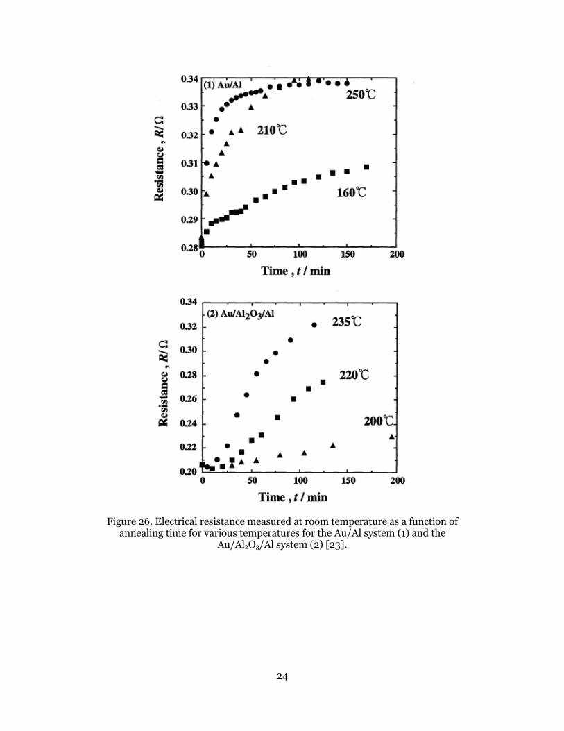
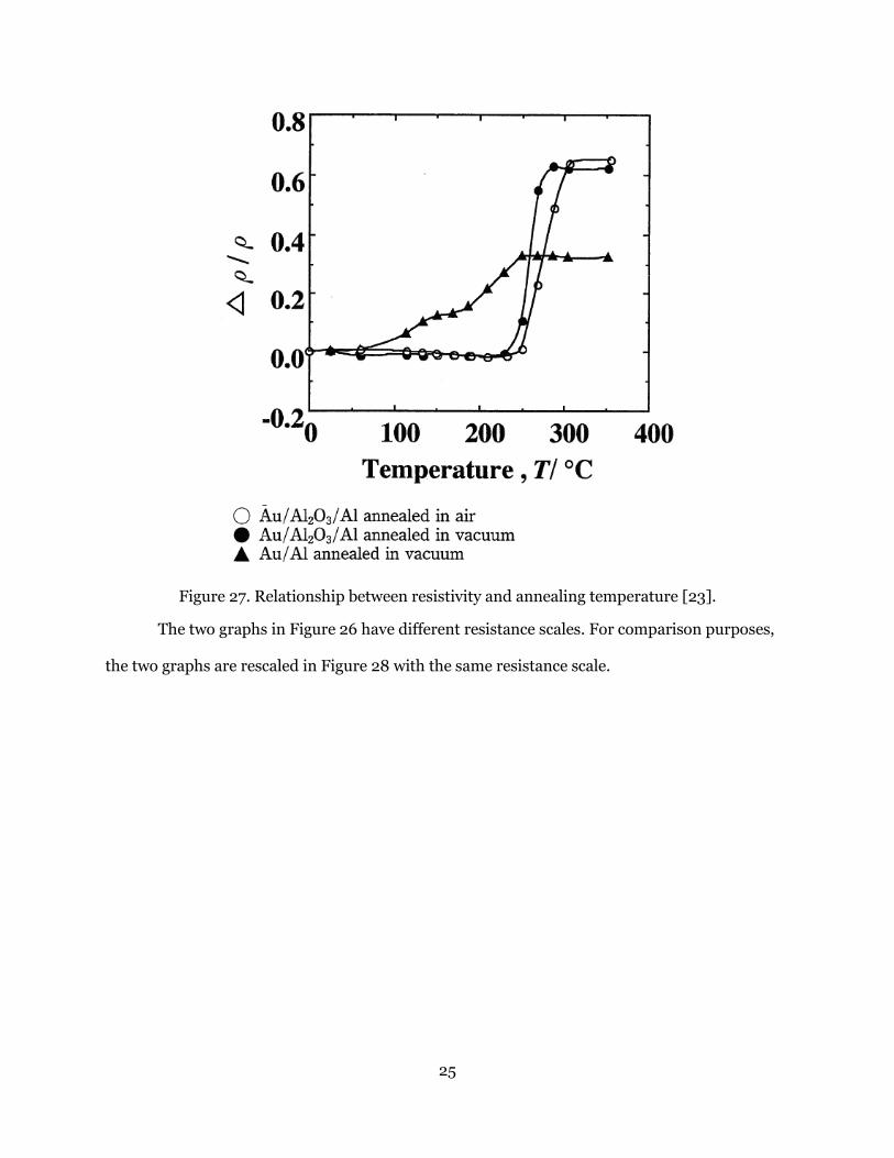
In 1995, Tsuge et al. studied “Gold Diffusion and Intermetallic Formation in Au/Al2O3/Al
Film” and reported resistance change behavior over time as shown in Figure 26 and Figure 27
[23].
24
Figure 26. Electrical resistance measured at room temperature as a function of annealing time for various temperatures for the Au/Al system (1) and the
Au/Al2O3/Al system (2) [23].
25
Figure 27. Relationship between resistivity and annealing temperature [23].
The two graphs in Figure 26 have different resistance scales. For comparison purposes,
the two graphs are rescaled in Figure 28 with the same resistance scale.
26
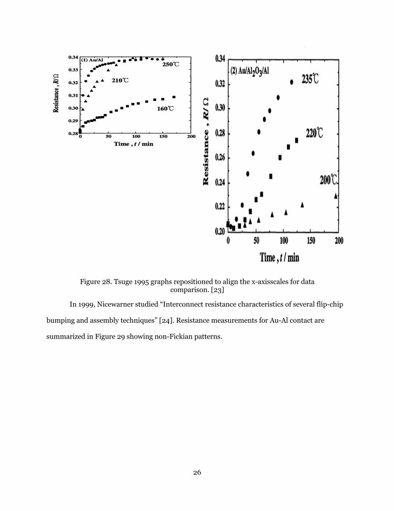
Figure 28. Tsuge 1995 graphs repositioned to align the x-axisscales for data comparison. [23]
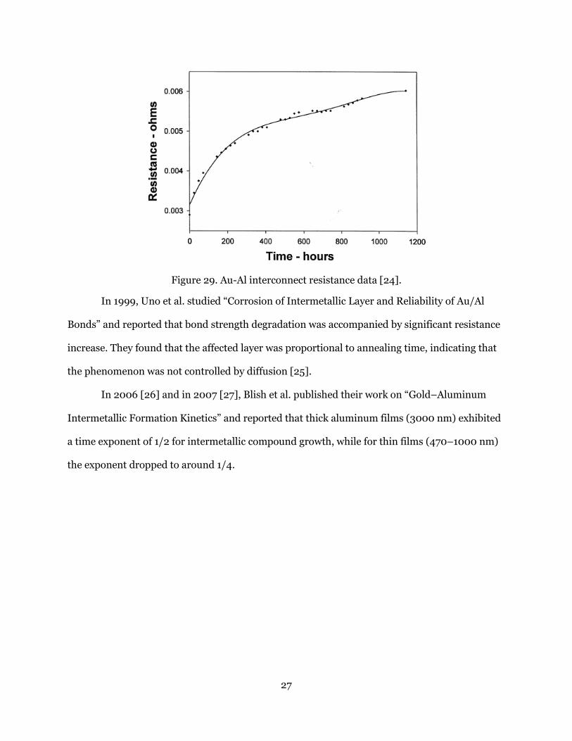
In 1999, Nicewarner studied “Interconnect resistance characteristics of several flip-chip
bumping and assembly techniques” [24]. Resistance measurements for Au-Al contact are
summarized in Figure 29 showing non-Fickian patterns.
27
Figure 29. Au-Al interconnect resistance data [24].
In 1999, Uno et al. studied “Corrosion of Intermetallic Layer and Reliability of Au/Al
Bonds” and reported that bond strength degradation was accompanied by significant resistance
increase. They found that the affected layer was proportional to annealing time, indicating that
the phenomenon was not controlled by diffusion [25].
In 2006 [26] and in 2007 [27], Blish et al. published their work on “Gold–Aluminum
Intermetallic Formation Kinetics” and reported that thick aluminum films (3000 nm) exhibited
a time exponent of 1/2 for intermetallic compound growth, while for thin films (470–1000 nm)
the exponent dropped to around 1/4.

28
4. PROBLEM DEFINITION
From the literature survey above, we see that the literature continues to point out
instances where the data does not correlate with a progression governed by diffusion and does
not follow the t½-law as expected. It appears that this issue existed all along, but was only
brought up and pointed out explicitly much later.
Table I. Various rates of diffusion found in literature
Fickian (t½) [28] for low temperature; [29] for small resistance increase only; [26] for thick Al film and lateral growth only
Linear [23] in the middle stage; [30] second stage at 150°C
Exponential [31] end of life; [8]; [18]; [25] Other [28]; [23]; [30]; [16]; [32]; [15]; [33];
[21]
To resolve this issue, one approach we can take is to review the phenomenon in its
geometrical construction. The initial resistance and later changes in the Au-Al wire bonds are
influenced by numerous factors:
1. The quality of initial bond affects the initial resistance of the interconnect and consequently
changes in its resistance.
2. The form of the interaction area between the two metals depends upon the process. The
amount of interaction area also influences the resistance of the bond.
3. The shape of the interaction area affects the way the intermetallic compounds and voids will
progress at the bond site.
4. After the bond has been made, changes in resistance are affected by the presence of
impurities, imperfections at the interface, gradual formation of the intermetallic
compounds, their by-products, and their interaction with materials present in the
surroundings.
5. Various intermetallic compounds have different rates of formation and differ in their
resistivity and strength until they reach an equilibrium.
29
6. The diffusion of the metals occurs at their interfaces.
7. The intermetallic formation process also generates Kirkendall voids. These voids contribute
to changes in the resistance of the interconnect.
8. Intermetallic compound and void formation is affected by the gases present in the
environment, depending on the level of their access to the system.
9. The gases affecting the intermetallic and void rates can come from the environment of an
un-encapsulated bond.
10. The sources of gaseous elements are also provided by the encapsulant materials surrounding
the bonds.
11. When the gases are entering from the sides of the interface, the void proliferation accelerates
laterally.
30
5. RESOLUTION TO THE PROBLEM OF RECONCILIATION OF NON-COMPLIANT DATA IN
REGARDS TO THE APPLICATION OF THE T½ LAW TO AU-AL WIRE BOND
DEGRADATION
The t½ law assumes diffusion in the perpendicular direction to the interface of the
diffusing materials. The Au/Al bond is a circular bond between two materials. Initial
intermetallic formation at the Au/Al interface proceeds in a direction perpendicular to the
interface; therefore, the measurements on its growth in various studies follows the t½ law. The
same scenario applies to the formation and growth of voids. As the voids follow the intermetallic
growth sequence, they also grow in the perpendicular direction following the t½ law, though
causing a lateral separation as they grow within a particular intermetallic layer.
The resistance of the bond interface increases due to the lateral spread of voids as it
continues to reduce the interface area as it progresses. As the growth of intermetallic in the z-
direction may follow t½ law, the resistance increase is dictated by how the voids decrease the
interfacial area of the Au-Al bond in the Au/Al bond plane. As the voids spread at the interface,
diffusion is no longer the dominant factor in resistance increase, and the amount and manner of
the spread of voids become the dominant factors in the increase of resistance at the interface.
The electrical resistance of an element can be computed as
𝑅𝑅 = 𝑟𝑟 𝐿𝐿𝐴𝐴 (2)
where L = Element length, A = Cross sectional area, r = Specific resistance. Reduction in the
element’s cross section, A, will translate into a proportionate increase in the element’s electrical
resistance.
Thickness of the interfacial disk is constrained as the voids start forming, rendering r × L
constant relative to the rapidly increasing reciprocal of A; and the resistance of the interface disk
varies with the inverse of the interfacial area, and behaves like a reciprocal function.
R ∝ A-1, r × L = constant for a wire bond (3)

31
Figure 30. Au-Al contact area of the interface disk decreases with time-temperature progression.
As the interface area decreases (Figure 30), the reciprocal value rapidly approaches
infinity just as a reciprocal function should.
R → ∞, with decreasing A as voids spread laterally at Au-Al interface (4)
The resistance of the portions of bond other than the interfacial disk are not affected
during thermal aging. Therefore, the significant change in resistance is contributed by the Au-Al
interfacial disk.
RAu-Al bond (total) = R (wire) + R (Au-Al interface), R (wire) = constant (5)
32
6. EVIDENCE AND SIMULATIONS TO RESOLVE THE NON-COMPLIANCE ISSUE
We can divide the processes taking place at the Au/Al interface into different stages over
the life of an Au-Al wire bond:
1. Formation of intermetallic compounds before the void formation starts.
2. Initiation of void formation at the interface.
3. Accelerated degradation as the voids spread laterally. The degradation rate may be further
accelerated by halides entering the Au-Al bond interface.
Each stage is evaluated below:
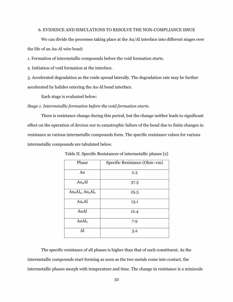
Stage 1. Intermetallic formation before the void formation starts.
There is resistance change during this period, but the change neither leads to significant
effect on the operation of devices nor to catastrophic failure of the bond due to finite changes in
resistance as various intermetallic compounds form. The specific resistance values for various
intermetallic compounds are tabulated below.
Table II. Specific Resistances of intermetallic phases [2]
Phase Specific Resistance (Ohm–cm)
Au 2.3
Au4Al 37.5
Au8Al3, Au5Al2 25.5
Au2Al 13.1
AuAl 12.4
AuAl2 7.9
Al 3.2
The specific resistance of all phases is higher than that of each constituent. As the
intermetallic compounds start forming as soon as the two metals come into contact, the
intermetallic phases morph with temperature and time. The change in resistance is a miniscule

33
part of the total resistance of the bond, as the intermetallic interface is quite thin and is limited
to a very small portion of the total wire bond including the significantly long Au wire.
R (wire) ≫ R (Au-Al interface), R (wire) ≈ constant before voids (6)
This reasoning is supported by scientific study. Among others, in 1966, K. Ono and T.
Kojima reported that the specific resistance of Al-Au compounds is not large enough to cause
abnormal increase in resistance [7].
Stage 2. Initiation of void formation at the interface.
Void formation (Figure 31) leads to significant increase in resistance and catastrophic
failure of the interface. As voids form, the interfacial area of the bond starts decreasing. The
bond fails due to the decreased contact area at the interface between Al and Au. Bond failure is
indicated by a rapid increase in resistance as can be predicted from Eq. 7.
ΔR ∝ Δ(A-1), r × L = constant for a wire bond (refer to eq. 3) (7)
Figure 31. Intermetallic growth with voids [34].
34
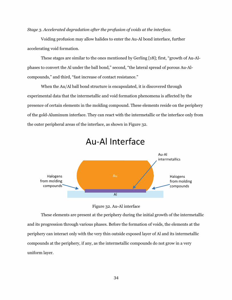
Stage 3. Accelerated degradation after the profusion of voids at the interface.
Voiding profusion may allow halides to enter the Au-Al bond interface, further
accelerating void formation.
These stages are similar to the ones mentioned by Gerling [18]; first, “growth of Au-Al-
phases to convert the Al under the ball bond,” second, “the lateral spread of porous Au-Al-
compounds,” and third, “fast increase of contact resistance.”
When the Au/Al ball bond structure is encapsulated, it is discovered through
experimental data that the intermetallic and void formation phenomena is affected by the
presence of certain elements in the molding compound. These elements reside on the periphery
of the gold-Aluminum interface. They can react with the intermetallic or the interface only from
the outer peripheral areas of the interface, as shown in Figure 32.
Figure 32. Au-Al interface
These elements are present at the periphery during the initial growth of the intermetallic
and its progression through various phases. Before the formation of voids, the elements at the
periphery can interact only with the very thin outside exposed layer of Al and its intermetallic
compounds at the periphery, if any, as the intermetallic compounds do not grow in a very
uniform layer.
35
As the interface between the molding compound and the Au-Al interface disk is not a
plane, any diffusion, though following the t½ law, will actually penetrate the disk faster than the
t½ law would dictate due to the disk geometry. As the disk is solid and very thin, this diffusion
may not proceed into the disk very fast and may not affect the void formation process very much
before the voids start forming and coalesce to allow outside gases to enter the interface.
If an attack of gases from the periphery of the solid interface disk were to take place, as
the outside elements would react with the peripheral intermetallic, the diameter of the circular
intermetallic disc would decrease as the reaction would progress inward from the periphery. The
reaction would progress with an increasing speed as the circle shrinks depending upon the
supply of gases from outside. Therefore, though the diffusion of the halides into the
intermetallic may follow t½-law, due to the shape of the intermetallic being a cylindrical thin
disk, the resulting diffusion rate may come out to be faster than what t½-law would predict.
Reported experimental data does not mention an effective or significant attack of halides
on the thin cylindrical Au-Al intermetallic disk to cause its shrinkage before the void formation
starts. Published cross-sectional images also fail to elicit such affect [4]. There exist data about
the role of gases from outside after they can penetrate through the inlets provided by the
formation of voids inside the intermetallic layer [1] [25] [35] [36] [37] [38].
As the voids start forming, the elements outside at the periphery find ever-increasing
openings to enter inside beyond the peripheral area to interact with a larger amount of
intermetallic phases. Therefore, before the formation of voids, the reaction rate and its
progression rate will be different compared to that after the voids start forming. With voids, the
reaction will progress even faster to accelerate the catastrophic failure of the bond, especially
due to the cylindrical shape of the disc they are penetrating or transforming, atom by atom,
aided by the increasing number of voids. Therefore, the resistance increase will no longer fit a t½
model. It will be a complex combination of various factors listed above.
36
In view of the above discussion, we consider the effect of various rates of void formation,
and simulate resistance behavior to observe the resulting bond life path.
For the purposes of this simulation, we assume that a 25 μm diameter gold wire is used
to make a gold-aluminum bond. A gold ball bond is produced in the gold wire bonding process
and is attached to the aluminum pad that produces a contact area with the aluminum pad equal
to twice the diameter of the wire, i.e., 50 μm diameter. The resulting area is equal to
πr2 = π (25 μm)2 = 1963.5 μm2.
For this simulation, r × L in Eq. 2 is constant, therefore,
R ∝ 1/A, as shown in Eq. 8.
𝑅𝑅 = α 1𝐴𝐴 (8)
We assume the initial resistance of this bond to be 50 mΩ. Substituting these values of
resistance and area in Eq. 8, results in a constant, α, of 98.1478, as shown in Eq. 9.
R × A = (0.05) (1963.5) = 98.1478 (9)
The initial area of the bond used in this simulation is an average area, since all bonds are
not exactly the same in an actual bonding process; they vary slightly, but not so much as to affect
the simulation results. Thus, a reciprocal of A0, A1, A2, A3, A4, …, An at corresponding times t0, t1,
t2, t3, t4, …, tn provides corresponding resistances R0, R1, R2, R3, R4, …, Rn. Therefore, we can use
the following relationship in Eq. 10 to determine resistance at tn for these assumed
circumstances.
Rn = 98.1478/An (10)
We consider the following three rates for the formation of voids: constant, decreasing,
and increasing, each resulting in a complete separation of the gold-aluminum interface after
3,000 hours, which is close to the actual data gathered at 175° C [31].

37
6.1. Constant Rate of Void Formation
For a constant rate of void formation, we assume that the total area is reduced by 1/100th
of the initial area (1963.5/100 = 19.635 μm2) every 30 hours, resulting in a lifespan of 3,000
hours.
6.2. Decreasing Rate of Void Formation
For a decreasing rate of void formation, we assume that voids start forming at a
decreasing rate, reducing area of the interface disc by an amount that decreases linearly every
time interval. Again, we use 100 equal time intervals of 30 hours each to yield a life span of
3,000 hours. For each interval, n, ranging from 1 to 100, the area is reduced by β × (101-n),
where β is calculated as shown in Eq. 11, and the corresponding resistance calculated according
to Eq. 10.
β = Initial Area / (1 + 2 + 3 +…+ 98 + 99 + 100)
= 1963.5 / 5050 = 0.38881 (11)
A decreasing rate of void formation could result from a diminishing supply of halides
from the molding compound surrounding an Au-Al bond.
6.3. Increasing Rate of Void Formation
We can also assume that voids at the Au-Al interface start forming slowly, and that the
rate of void formation increases as time progresses. An increasing rate of void formation can
result from halides entering the interface and accelerating the void formation phenomenon [31].
Heat releases halides from the molding compounds, which will enter the interface as voids
create openings around the periphery of the bond.
For this scenario, we again use 100 equal time intervals of 30 hours each for a resulting
life span of 3,000 hours. For each interval, n, ranging from 1 to 100, the area is reduced by β × n,
where β is calculated as shown in Eq. 11, and the corresponding resistance calculated according
to Eq. 10.
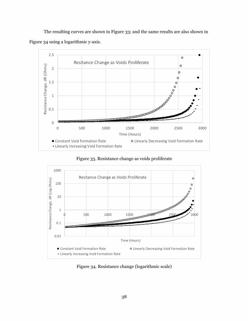
38
The resulting curves are shown in Figure 33; and the same results are also shown in
Figure 34 using a logarithmic y-axis.
Figure 33. Resistance change as voids proliferate
Figure 34. Resistance change (logarithmic scale)

39
The three models of area decrease may be written in a simpler way.1 The models are
exactly the same as above, except that the number of time steps has been changed from “100” to
“N”, and the N → ∞ limit has been taken, giving simpler expressions.
Table III gives three models of change of area, which are used to analyze the data; and
Figure 35 plots the normalized models. In the table, Ainit is the initial cross-section of
conducting area of the wire bond, and t0 is defined as the age at which the conducting area goes
to zero (so the resistance goes to infinity). That is, t0 is the lifetime of the bond as determined by
the time to go electrically open. The age of the bond is t where t < t0. τ is the age of the bond
normalized to the lifetime.
Table III. Three models of conductive (non-voided) bond area as a function of age.
Area Reduction Rate vs Age
Reduction Rate Model
Area vs Age Normalized Age
Constant. init 0dA dt A t= − ( )init( ) 1A t A τ= −
0
tt
τ = Decreases Linearly init 02( )(1 )dA dt A t τ= − − ( )2init( ) 1A t A τ= −
Increases Linearly init 02( )dA dt A t τ= − ( )2
init( ) 1A Aτ τ= −
1 The treatment from here to equation 18 is courtesy of Dr Glen Shirley included in acknowledgements.

40
Figure 35. Plots of Area vs Age (left) and Resistance (reciprocal of Area) vs Age for each of the three models of bond area reduction rate given in Table III.
6.4. Equivalence of the Three Models
The derivations below show that the three different models are effectively the same.
Rate of Reduction of A with Age is Constant
When the rate of area decrease is constant,
init
0
dA Adt t
= − (12)
and elementary integration gives
0
0.1
0.2
0.3
0.4
0.5
0.6
0.7
0.8
0.9
1
0 0.1 0.2 0.3 0.4 0.5 0.6 0.7 0.8 0.9 1
A(t)/
Aini
t
Tau
Area vs Rate of Decrease
ConstantLinear DecreaseLinear Increase
1
10
100
1000
10000
0 0.1 0.2 0.3 0.4 0.5 0.6 0.7 0.8 0.9 1
Aini
t/A(t)
Tau
Resistance vs Rate of Decrease
ConstantLinear DecreaseLinear Increase
41
( )init 0( ) 1 where A t A t tτ τ= − = (13)
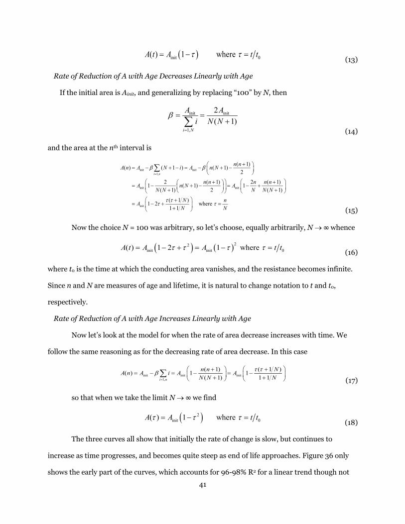
Rate of Reduction of A with Age Decreases Linearly with Age
If the initial area is Ainit, and generalizing by replacing “100” by N, then
init init
1,
2( 1)
i N
A Ai N N
β
=
= =+∑
(14)
and the area at the nth interval is
init init1,
init init
init
( 1)( ) ( 1 ) ( 1)2
2 ( 1) 2 ( 1)1 ( 1) 1( 1) 2 ( 1)
( 1 )1 2 where 1 1
i n
n nA n A N i A n N
n n n n nA n N AN N N N N
N nAN N
β β
τ ττ τ
=
+ = − + − = − + −
+ + = − + − = − + + + +
= − + = +
∑
(15)
Now the choice N = 100 was arbitrary, so let’s choose, equally arbitrarily, N → ∞ whence
( ) ( )22init init 0( ) 1 2 1 where A t A A t tτ τ τ τ= − + = − =
(16)
where t0 is the time at which the conducting area vanishes, and the resistance becomes infinite.
Since n and N are measures of age and lifetime, it is natural to change notation to t and t0,
respectively.
Rate of Reduction of A with Age Increases Linearly with Age
Now let’s look at the model for when the rate of area decrease increases with time. We
follow the same reasoning as for the decreasing rate of area decrease. In this case
init init init
1,
( 1) ( 1 )( ) 1 1( 1) 1 1i n
n n NA n A i A AN N N
τ τβ=
+ += − = − = − + +
∑ (17)
so that when we take the limit N → ∞ we find
( )2init 0( ) 1 where A A t tτ τ τ= − =
(18)
The three curves all show that initially the rate of change is slow, but continues to
increase as time progresses, and becomes quite steep as end of life approaches. Figure 36 only
shows the early part of the curves, which accounts for 96-98% R2 for a linear trend though not

42
exactly linear. Figure 37 shows the latter part of the curves with 82-86% R2 for an exponential
trend as they approach end of life, but do not have an exponential dependence.
Figure 36. Resistance Change (early trend)
Figure 37. Resistance change (end of life trend)
43
The degradation behavior of the system governed by the proliferation of voids at the
gold-aluminum interface can be divided into two parts. The first part represents a slower
increase in resistance close to a linear trend, though not exactly linear. The second part
represents a rapidly increasing resistance that approaches close to an exponential trend at the
end of life, though it is not exactly exponential. The simulations show that factors additional to
Kirkendall voiding must be considered to obtain a model to explain various observed trends,
which fit the previously obtained data summarized in Table I.
6.5. Summary of Rates of Void Formation
These calculations do not consider the early intermetallic growth before the initiation of
voids, since this phase only results in minimal resistance change [7]. The actual environment
may be a combination of the above scenarios, resulting in its own unique behavior. Other
scenarios for the rate of void formation could be considered, but the ones presented herein
provide the necessary information to show that a deviation from Fickian behavior is correlated
to the void formation rate at the Au-Al interface, though not completely explained.
6.6. Case of Circular Initiation and Progression of Intermetallic Compounds in the Au-Al
Interfacial Disc
In some instances, the intermetallic compounds, and therefore void formation, has been
observed to initiate and propagate in a circular manner at the Au-Al interface [29] [34]. This
scenario also addresses the instances, as mentioned above, where void formation is mostly
governed by the influx of gases from outside the periphery of the Au-Al intermetallic interfacial
disc, which accelerate intermetallic formation within the interfacial disc. In this case, again the
above three scenarios are applicable. We can also look at this case as a circle decreasing in
diameter as voids proliferate towards the inside of the circle until they reach its center and
entirely separate the bond. Hence, the resistance, R, of the interface will depend on the
decreasing area, A, of the circle at the interface, and will vary with the inverse of the interfacial
area, as already analyzed in the previously discussed cases.

44
7. CONCLUSIONS AND FUTURE WORK
The Au-Al bond degradation in semiconductor applications can be divided into three
phases. Resistance increase in the first phase of degradation is purely due to Au-Al diffusion and
follows the t½ law. Resistance increase in the second and third phases is dominated by the rate
of formation of Kirkendall voids. This dissertation shows why the resistance increase, and thus
the failure rate, in the final two phases of Au-Al wire bond degradation may not follow the t½ law
for diffusion-driven phenomenon, and may show non-Fickian resistance increase despite the
degradation being driven by diffusion. Results of constant, increasing, and decreasing rates of
void formation show deviations from Fickian trends. The case of circular progression of voids
has also been analyzed.
This work uses published experimental data for comparison with and validation of the
developed simulations. For future work, new experimental data could be collected to validate
the simulations.

45
REFERENCES
[1] S. S. Ahmad, R. C. Blish II, T. J. Corbett, J. L. King and C. G. Shirley, "Effect of Bromine in
Molding Compounds on Gold-Aluminum Bonds," IEEE Transactions on Components,
Hybrids, and Manufacturing Technology CHMT-9, vol. 9, no. 4, pp. 379-385, 1986.
[2] G. Harman, Wire Bonding in Microelectronics, McGraw-Hill, 2010.
[3] R. G. Oswald, W. R. R. d. Miranda and C. W. White, "Changes in Strength and Resistance
of Aluminum to Gold Ultrasonic Bonds after Temperature, Electrical, and Environmental
Stress," Proceedings 1975 International Microelectronics Symposium, pp. 324-339, 1975.
[4] P. K. Footner, B. P. Richards, C. E. Stephens and C. T. Amos, "A Study of Gold Ball Bond
Intermetallic Formation in PEDs using Infra-Red Microscopy," in 24th Annual Reliability
Physics Symposium, April 1986.
[5] L. E. Miller and I. M. Mackintosh, "Semiconductor Reliability," in Conference on
Reliability of Semiconductor Devices Edited by John E. Schwop, Harold J, Sullivan,
Engineering Publishers, 1961, pp. 107-107.
[6] W. M. Berger, R. S. Keen and G. L. Schnable, "Reliability Phenomena in aluminum
metallizations on silicon dioxide," Symposium on Physics of Failure in Electronics, pp. 1-
31, 1966.
[7] K. Ono and T. Kojima, "Some Problems of Au Lead Wire in Semiconductor Devices," Rev.
of the Electr. Commun. Laboratory, NTT, vol. 15, no. 10, pp. 141-151, 1966.
[8] R. Keen, L. Loewenstern and G. Schnable, "Mechanisms of Contact Failure in
Semiconductor Devices," Proceedings of IEEE Sixth Annual Reliability Physics
Symposium, pp. 216-233, November 1967.
46
[9] G. K. C. Chen, "On the Physics of Purple Plague Formation, and the Observation of Purple
Plague in Ultrasonically Joined Gold-Aluminum Bonds," IEEE Transactions on Parts,
Materials and Packaging PMP-3, no. No. 4, December, pp. 149-153, 1967.
[10] J. Linde, Thesis, Stockholm: Cited in A. N. Gerritsen and J. O. Linde, Physica 18 (1952):
877, 1939.
[11] J. H. Anderson Jr. and W. P. Cox, "Failure Modes in Gold-Aluminum Thermocompression
Bonds," IEEE Transactions On Reliability, no. November, pp. 206-207, 1969.
[12] S. Goldfarb, "Wire Bonds on Thick Film Conductors," in Proceedings 21st Electronic
Components Conference, 1971.
[13] W. R. d. Miranda and R. Oswald, "Changes in Strength and Resistance After Burn-In of
Aluminum Wire Bonds to Thick and Thin Film Gold," in International Society of Hybrid
Microelectronics, proceedings of, 1974, 1974.
[14] A. N. Gerritsen and J. O. Linde, "The Electrical resistances of Allys of a Noble Metal and a
Transition Metal," Physica, vol. 18, no. 11, pp. 877-890, 1952.
[15] R. B. Belser, "Alloying Behavior of Thin Bimetal Films, Simultaneously or Successively
Deposited," J. Appl. Phys., vol. 31, no. 3 (March), p. 562, 1960.
[16] G. A. Dodson, "Aging Problems of Thermocompression Bonds Made to Semiconductor
Devices," IRE Trans. Electron Devices, Vols. ED-9, no. November, p. 506, 1962.
[17] G. L. Schnable, R. S. Keen and L. R. Loewenstern, "Study of Contact Failures in Integrated
Circuits - Final Report Contract AF30(602)-4034," Philco-Ford Corp. for the Rome Air
Development Center, Griffiss Air Force Base, N. Y., 1967.
[18] W. Gerling, "Electrical and Physical Characterization of Gold-Ball Bonds on Aluminum
Layers," Proceedings IEEE Electronic Components Conference, pp. 13-20, 1984.

47
[19] L. Maiocco, D. Smyers, P. Munroe and I. Baker, "Correlation between Electrical Resistance
and Microstructures," IEEE Trans. Compon. Hybrids Manuf. Technol., vol. 13, pp. 592-
595, 1990.
[20] Y. L. Corcoran, A. H. King, N. d. Lanerolle and B. Kim, "Grain boundary diffusion and
growth of titanium silicide layers on silicon," J. Electron. Mater., vol. 19, no. November, p.
1177–1183, 1990.
[21] R. M. Murcko, R. A. Susko and J. M. Lauffer, "Resistance Drift in Aluminum to Gold
Ultrasonic Wire Bonds," IEEE Transactions On Components, Hybrids, And
Manufacturing Technology, vol. 14, no. 4 (December 1991), pp. 843-847.
[22] V. Koeninger, H. H. Uchida and E. Fromm, "Degradation of gold-aluminium ball bonds by
aging and contamination," IEEE Transactions on Components and Packaging
Technologies Hybrids Manufacturing Technology, vol. 18, no. 4, pp. 835-841, 1995.
[23] A. Tsuge, K. Mizuno, T. Uno and K. Tatsumi, "Gold Diffusion and Intermetallic Formation
in Au/Al2O3/Al Film," J. Japan lnst. Metals, vol. 59, no. 11, pp. 1095-1102, 1995.
[24] E. Nicewarner, "Interconnect resistance characteristics of several flip-chip bumping and
assembly techniques," Microelectronics Reliability, vol. 39, pp. 113-121, 1999.
[25] T. Uno and K. Tatsumi, "Corrosion of Intermetallic Layer and Reliability of Aul Al Bonds,"
J. Japan Inst. Metals, vol. 63, no. 3, pp. 406-415, 1999.
[26] R. Blish, S. Li, H. Kinoshita, S. Morgan and A. Myers, "Gold-Aluminum Intermetallic
Formation Kinetics," in Reliability Physics Symposium Proceedings, 2006. 44th Annual.,
IEEE International, 26-30 March 2006.
[27] R. C. Blish, S. Li, H. Kinoshita, S. Morgan and A. F. Myers, "Gold–Aluminum Intermetallic
Formation Kinetics," IEEE Transactions on Device and Materials Reliability, vol. 7, no. 1,
pp. 51-63, 2007.
48
[28] L. Maiocco, D. Smyers, P. Munroe and I. Baker, "Correlation between Electrical Resistance
and Microstructures," IEEE Trans. Compon. Hybrids Manuf. Technol., vol. 13, pp. 592-
595, 1990.
[29] V. Koeninger, H. H. Uchida and E. Fromm, "Degradation of gold-aluminium ball bonds by
aging and contamination," IEEE Transactions on Components and Packaging
Technologies Hybrids Manufacturing Technology, vol. 18, no. 4, pp. 835-841, 1995.
[30] E. Nicewarner, "Interconnect resistance characteristics of several flip-chip bumping and
assembly techniques," Microelectronics Reliability, vol. 39, pp. 113-121, 1999.
[31] S. S. Ahmad, R. C. Blish II, T. J. Corbett, J. L. King and C. G. Shirley, "Effect of Bromine in
Molding Compounds on Gold-Aluminum Bonds," IEEE Transactions on Components,
Hybrids, and Manufacturing Technology CHMT-9, vol. 9, no. 4, pp. 379-385, 1986.
[32] A. N. Gerritsen and J. O. Linde, "The Electrical resistances of Alloys of a Noble Metal and
a Transition Metal," Physica, vol. 18, no. 11, pp. 877-890, 1952.
[33] Y. L. Corcoran, A. H. King, N. d. Lanerolle and B. Kim, "Grain boundary diffusion and
growth of titanium silicide layers on silicon," J. Electron. Mater., vol. 19, no. November, p.
1177–1183, 1990.
[34] J. Watson and G. Castro, "Castro High-Temperature Electronics Pose Design and
Reliability Challenges," Analog Dialogue, vol. 46, no. 4, pp. 1-7, April 2012.
[35] M. M. Khan and H. Fatemi, "Gold-Aluminum Bond Failure Induced by Halogenated
Additives in Epoxy Molding Compounds," in Proceedings of the 1986 International
Symposium on Microelectronics, Georgia World Congress Center, Atlanta, Georgia,
October 6-8, 1986.
49
[36] M. Khan, H. Fatemi, J. Romero and E. Delenia, "Effect of High Thermal Stability Mold
Material on the Gold-Aluminum Bond Reliability in Epoxy Encapsulated VLSI Devices,"
12-14 April 1988.
[37] C. S. Wang, D. B. Fritz and A. Mendoza, "Chemistry of Stable Brominated Epoxies," in
Polymeric Materials for electronic packaging and interconnection, Washington DC,
American Chemical Society, 1989, pp. 397-404.
[38] T. Uno, S. Terashima, K. Onoue and K. Tatsumi, "Improvement in thermal reliability in
gold-aluminum bonds encapsulated in bi-phenyl epoxy resin," Proceedings of the SPIE -
The International Society for Optical Engineering 1999, 1998 International Symposium
on Microelectronics , vol. 3582, pp. 591-596, 1999.