Embed Size (px)
Citation preview

China Semiconductor Technology International Conference 2013 (CSTIC 2013)
Q. Lin IBM Thomas J. Watson Research Center Yorktown Heights, New York, USA
C. Claeys imec Leuven, Belgium
D. Huang Pall Inc. Port Washington, New York, USA
H. Wu Semiconductor Manufacturing International Corporation Shanghai, China
Y. Kuo Texas A&M University College Station, Texas, USA
R. Huang Peking University Beijing, China
K. Lai IBM Semiconductor Research and Development Center Hopewell Junction, New York, USA
Y. Zhang Applied MaterialsSanta Clara, California, USA
Z. Guo Intel Corporation Portland, Oregon, USA
S. Wang Anji Microelectronics(Shanghai) Co. Ltd. Shanghai, China
R. Liu Fudan University Shanghai, China
T. Jiang Maxim Integrated Products Inc. Sunnydale, California, USA
P. Song IBM Thomas J. Watson Research Center Yorktown Heights, New York, USA
C. Lam IBM Thomas J. Watson Research Center Yorktown Heights, New York, USA
J. Xiong IBM Thomas J. Watson Research CenterYorktown Heights, New York, USA
K. Chen IBM Albany, New York, USA
Editors:
Published by
The Electrochemical Society65 South Main Street, Building DPennington, NJ 08534-2839, USAtel 609 737 1902fax 609 737 2743www.electrochem.org
TM
Vol. 52, No. 1

Copyright 2013 by The Electrochemical Society.All rights reserved.
This book has been registered with Copyright Clearance Center.For further information, please contact the Copyright Clearance Center,
Salem, Massachusetts.
Published by:
The Electrochemical Society65 South Main Street
Pennington, New Jersey 08534-2839, USA
Telephone 609.737.1902Fax 609.737.2743
e-mail: [email protected]: www.electrochem.org
ISSN 1938-6737 (online)ISSN 1938-5862 (print)
ISSN 2151-2051 (cd-rom)
ISBN 978-1-60768-382-7 (CD-ROM)ISBN 978-1-60768-381-0 (PDF)
ISBN 978-1-62332-030-0 (Softcover)
Printed in the United States of America.

iii
PREFACE This issue of the ECS Transactions contains a portion of the accepted papers to be
presented at China Semiconductor Technology International Conference 2013 (CSTIC 2013) to be held March 17th and 18th 2013 in Shanghai, China. The compact disc (CD) version of these papers will serve as CSTIC 2013 conference proceedings and will be distributed to registered conference attendees.
CSTIC is the largest and the most comprehensive annual industrial semiconductor
technology conference in China. It aims to provide a platform for executives, managers, engineers and researchers from around the world to exchange the latest developments in semiconductor technology and manufacturing and related fields. It also offers an opportunity for those who are interested in investing and collaboration opportunities in the semiconductor industry in Asia, particularly in China.
CSTIC covers all the aspects of semiconductor technology and manufacturing, including
circuit design, devices, materials, patterning (lithography and etching), processes, integration, testing, reliability, and manufacturing as well as emerging semiconductor technologies, including clean energy such as light emitting diodes (LEDs), III-V semiconductors and Microelectromechanical systems (MEMS).
CSTIC 2013 added a new symposium on Circuit Design, System Integration and
Applications to meet the technology needs of a large (more than 250) and growing number of chip design houses in China.
CSTIC 2013 continued the fine tradition of this conference to have a broad international representation and attracted more than 350 paper submissions from around the world. These papers were from all major semiconductor manufacturing regions in the world, including China, Europe, Japan, Korea, and the United States. About 250 papers have been selected for oral presentations and approximate 60 papers for poster presentations after careful reviews by the conference organizing committee. Among the accepted papers, approximately half of the papers percent are from outside China.
More than 150 papers are included in this ECS Transactions issue after peer reviews.
They represent a snapshot of the recent developments in semiconductor technology and manufacturing in the world. In particular, they offer a glimpse into the state-of-the-art of semiconductor technology and manufacturing in China. These papers are divided into eleven (11) sections according to the eleven symposia of CSTIC 2013. They are:
• Device Engineering and Technology • Lithography and Patterning • Dry & Wet Etch and Cleaning • Thin Film Technology • Chemical-Mechanical Polishing (CMP) and Post-CMP Cleaning • Materials and Process Integration for Devices and Interconnections • Packaging and Assembly • Metrology, Reliability and Testing • Emerging Semiconductor Technologies • Advances in MEMS and Sensor Technologies • Circuit Design, System Integration and Applications

iv
We hope that this ECS Transactions issue and the CSTIC 2013 proceedings will prove
valuable to the engineers and the researchers in the fast-moving and growing semiconductor industry. We also hope that it will help readers understand the status of semiconductor technology and manufacturing in China. We further hope that it will also serve as a useful reference for those who are interested in nanofabrication, micro- and nano-fluidics, micro- and nano-photonics, organic electronics, bio-chips, photovoltaic (PV), light emitting diode (LED) and other clean energy technologies.
We thank the invited speakers and the authors, particularly the conference plenary
speakers, Professor Ivar Giaever, Nobel laureate and professor of Rensselaer Polytechnic Institute, USA, Dr. Ghavam Shahidi, IBM Fellow and director of silicon technology, IBM Thomas J. Watson Research Center, USA, Dr. Peng Bai, Vice President, technology and manufacturing group, Intel, USA, for their valuable contributions to CSTIC 2013. We also thank the more than 120 organizing committee members, particularly the symposium chairs, for their dedication and hard work to help improve the quality and broaden the reach of CSTIC. These committee members are experts in their respective fields of semiconductor technology and are from well-known companies or prestigious institutions. They all have demanding day jobs, yet they have volunteered to devote the 25th, 26th hour of their days to help organize this conference and to review papers presented in this ECS Transactions issue. We are grateful for their contributions to the semiconductor community. We are also indebted to the financial support from the sponsors of CSTIC 2013. Finally, we extend our sincere thanks to the SEMI and the ECS staff for their tireless efforts and their meticulous organizational skills to help organize CSTIC 2013 and to assemble and publish this ECS Transactions issue and the CSTIC 2013 proceedings CD.
Qinghuang Lin, Chair, CSTIC 2013
IBM Thomas J. Watson Research Center Yorktown Heights, New York, USA
CSTIC 2013 Organizing Committee
17 March 2013, Shanghai, China

v
ECS Transactions, Volume 52, Issue 1 China Semiconductor Technology International Conference 2013 (CSTIC 2013)
Table of Contents Preface iii
Chapter 1 Design and Device Engineering
(Invited) Technologies and Challenges of Fine Pitch Backside Via-Last TSV Process Integration for 3DIC Applications
T. Ku, C. H. Lin, P. J. Tzeng, E. H. Chen, T. C. Hsu, S. C. Chen, C. C. Wang, J. C. Chen, C. C. Chen, Y. C. Hsin, S. C. Liao, P. C. Chang, Y. M. Lin, Y. H. Chang (Industrial Technology Research Institute)
3
HKMG All Last to Meet 20nm Logic Device Challenge
X. Xie, J. Ju, S. Yu, F. Fu, J. Zhao, Y. Chen, H. Liu, Z. Zhang, Q. Han, W. Bu, M. Liao, Y. Li (Semiconductor Manufacturing International Corporation), J. Tao (Shanghai University), J. Yan, H. Yang (IME)
7
(Invited) Innovative Wide Band Gap Power Devices Achievements in ITRI
C. Y. Lee, Y. H. Chen, L. S. Lee, C. C. Hung, C. T. Yen, S. F. Lin, R. Xuan, W. H. Kuo, M. J. Tsai (ITRI)
11
A Novel Deep–Oxide Trench SOI–LIGBT with a P–Pillar Layer
Q. Fu, B. Zhang, Z. Li (University of Electronic Science and Technology of China) 17
PNP Transistor Design and Simulation in SiGe BiCMOS with Low Cost and High Performance
D. Liu, J. Shi, J. Hu, W. Duan, P. Ci, J. Pan, F. Chen, X. Chen, J. Huang, W. Qian, X. Xu, S. Xiao, T. Chu (Shanghai Huahong NEC Electronics Company)
23
A Comprehensive Study of SiGe Source/ Drain Local Stress by Nano Beam Diffraction
L. Jin, H. Tu, Y. He, Y. He, J. Wu (Semiconductor Manufacturing International Corporation)
33

vi
Ti/HfO2 Based RRAM Operation Voltage Scaling for Embedded Memory C. H. Tsai, F. T. Chen, H. Y. Lee, Y. S. Chen, K. H. Tsai, T. Y. Wu, S. Z. Rahaman, P. Y. Gu, W. S. Chen (Industrial Technology Research Institute), P. S. Chen (Minghsin University of Science and Technology), Z. H. Lin, P. L. Tseng, W. P. Lin, C. H. Lin, S. S. Sheu, M. J. Tsai, T. K. Ku (Industrial Technology Research Institute)
39
A Novel Programming Method for Multilevel RRAM Based on Pulse Width Modulation
C. Chen, Y. Cai, S. Yin, R. Huang (Peking University)
45
Optimization of HfO2 Growth Process by Atomic Layer Deposition (ALD) for High Performance Charge Trapping Flash Memory Application
G. Chen, Z. Huo, S. Zhao, X. Yang, Z. Liu, M. Zhang, Z. Sun, Y. Han, D. Zhang, C. Wang, Y. Chu (Chinese Academy of Sciences), S. Liu (Lanzhou University), M. Liu (Chinese Academy of Sciences)
51
(Invited) Revisiting the Impact on Sub-Threshold Regions in Uniaxially-Strained FETs
M. H. Na, K. McStay, E. J. Nowak (IBM) 57
Diamond-Shaped e-SiGe Optimization by TCAD Simulation to Improve P-type MOSFET Performance for 28nm Logic Technology and Beyond
H. Wu, Z. Pan, X. Shi, B. Lee, Y. Ding, F. He, B. Ye, T. Yu, Y. He, H. Zhang, S. Yu (Semiconductor Manufacturing International (Shanghai) Corporation)
61
Simulations of Bulk FinFETs with Body Gate Controlling Punch through Leakage
M. Xu, H. Zhu, H. Wu, Q. Liang, H. Yin, D. Cheng, T. Ye (Chinese Academy of Sciences)
67
(Invited) Negative-Bias Temperature Instability – Insight from Recent Dynamic Stress Experiments
D. S. Ang, A. A. Boo, Y. Gao (Nanyang Technological University)
73
Low-Frequency Noise in High-K and SiO2 UTBOX SOI nMOSFETS
S. D. dos Santos, J. A. Martino (University of São Paulo), V. Strobel, B. Cretu, J. M. Routoure, R. Carin (University of Caen), E. Simoen, M. Aoulaiche, M. Jurczak, C. Claeys (imec)
87
(Invited) Comparative Study for SRAM Cells in Near and Sub-Threshold Region
Y. H. Yang, J. H. Park (Yonsei University), S. C. Song, F. B. Yang, J. Wang, G. Yeap (Qualcomm Inc.), S. O. Jung (Yonsei University)
93

vii
Ultra Low Power 6T SRAM Cell Designed on 65nm Low Power Technology Platform Suitable for High Temperature Applications
L. Jinhua, J. Zhou, A. Zhou, J. Chen, S. Huang, J. Ning, S. Yu (SMIC (BJ))
99
A New High Speed Low Power Dissipation Three-Element Si-Based SRAM Cell
X. Tong, H. Wu, L. Zhao, H. Zhong (Chinese Academy of Sciences) 105
High Density Low Leakage SRAM Standby Current Reduction with a Channel Stop Implant in p-Type Well in 40nm CMOS Development
Y. Li (SMIC), J. Tao (Shanghai University), S. K. Huang, D. Lin, S. Zhang, J. Ju, D. Jin, S. Yu (SMIC)
111
Electrical Properties and Interfacial Structures of High-k/Metal Gate MOSCAP Using Ti/TiN Scavenging Stack between High-κ Dielectric and Metal Gate
X. Ma, X. Wang, K. Han, W. Wang, H. Yang, C. Zhao, D. Chen, T. Ye (Chinese Academy of Sciences)
117
A Study on the AA/STI Corner Shape Impact on Narrow Width MOSFET Idsat/Ioff Performance for 28nm Technology Node
Y. Pu, X. Shi, J. Kim, S. Yu (Semiconductor Manufacturing International (Shanghai) Corporation)
123
Impacting Factors and Improvement for Within-Shot IDSAT Uniformity
J. Tao (Shanghai University), Y. Li (SMIC), W. Shi (Shanghai University), D. Jin, H. Li, Z. Fan, F. Fan, T. Chang, S. Zhu, J. Ju, S. Yu (SMIC)
129
Chapter 2 Lithography and Patterning
(Invited) Patterning Process Model Challenges for 14 Nm
J. L. Sturtevant (Mentor Graphics Corp.) 137
(Invited) Advanced Modeling for Full-Chip Low-k1 Lithography Simulations
P. Liu (Brion Technologies Inc.) 147
(Invited) Efficient Mask Synthesis with Augmented Lagrangian Methods in Computational Lithography
J. Li, E. Y. Lam (The University of Hong Kong)
163

viii
Substrate Induced Overlay Non-Uniformity Study L. Wang, H. Meng, Y. Liu, X. Guo, Q. Sun, S. Xiao (Shanghai Huahong NEC Electronics Company, Ltd)
169
Substrate effect on CD Control for Ion Implantation Layer Lithography Beyond 45 nm Node
H. Hu, L. Ding, J. Pei, M. Shen, X. Shi, Q. Wu, Q. Liu, Y. Lin, Y. Gu (Semiconductor Manufacturing International Corp.)
177
Evolution of Dual-Layer Patterning Film for Lithography Applications
Q. Chai, X. Liang, Y. Chen, X. Li, G. Zhao (Applied Materials China) 183
Improvement of Contact OPC Model Accuracy by Using Corner Chopping
Y. Huang, W. Zhang, Q. Liu, X. Shi, Y. Gu (Semiconductor Manufacturing International Corp.), F. Shao, L. Zhang, Y. Zhu, C. Du (Mentor Graphics Corporation)
187
Study Of Gate Critical Dimension Uniformity (CDU) Budget and Improvement at 28nm Node
Q. Shu, Q. Wu, Y. Zu, T. Wang, S. Zhang, T. Li, Y. Lin, Y. Gu (Semiconductor Manufacturing International Corp.)
193
Process Optimization Using OPE-Master and CDU Master
C. Shao (Nikon Precision China), K. Takehito, T. Fujiwara, T. Matsuyama (Nikon Corporation)
199
Accurate Matching for CDSEM on ADI Wafers
W. H. Li, Y. S. Lin, S. F. Yang, B. X. Cai, Y. Huang (Semiconductor Manufacturing International Corporation)
213
The Focus Margin Gain and Limitation Realized by Focus Drilling in 28 nm Hole-Like Design Rules
T. Li, G. Deng, J. Hao, G. Li, Q. Wu (Semiconductor Manufacturing International Corp.)
221
(Keynote) Advanced Lithography for Density Scaling
M. L. Rieger (Synopsys, Inc.) 227
(Invited) Development of Mask 3D Virtual Aberration Model to Predict Pattern Best Focus Deviation
K. Fujii, M. Imai (Nikon Corporation), L. Qunying (Institute of Microelectronics)
233

ix
(Invited) Negative Tone Development Process and Resist Materials with ArF Immersion Exposure Process
S. Tarutani (FUJIFILM Corporation)
239
(Invited) Development Status of EUV Resist toward Sub-20nmhp
T. Kimura (JSR Corpration) 245
Robust Trilayer Patterning Technique
Z. Zhu, M. Weigand, V. Krishnamurthy, D. Sullivan (Brewer Science Inc.) 251
New Approach for Reducing the Out of Band effect and Outgassing by Applying Top Coat Materials
R. Sakamoto, R. Onishi, N. Fujitani, B. C. Ho (Nissan Chemical Industries, Ltd.)
259
Limitation of Layout Correction on Improvement of OPC Model Calibration
K. Wang, X. Shen, J. Xing, Q. Liu, X. Shi, K. Wu, Y. Gu (Semiconductor Manufacturing International Corp.), R. Zhang, Y. Zhu, F. Shao, C. Du (Mentor Graphics Corp.)
267
Chapter 3 Dry and Wet Etch and Cleaning
(Invited) Applications Of A Low Te Plasma To finFET FEOL Etch Challenges
Q. Yang (TEL Technology Center of America), L. Chen (Tokyo Electron America) 275
(Invited) Important Challenges in Double Patterning Processes
H. Yaegashi (Tokyo Electron LTD), K. Oyama, A. Hara, S. Natori, S. Yamauchi, M. Yamato (LPDC Advanced Patterning Gr.)
281
Identification and Characterization of a Subtle Bump Defect Formed Upon Organic Mandrel in a Self-Aligned Double Patterning Process
Z. Yang, F. H. Hsu, K. L. Wei, H. J. Lee, N. T. Lian, T. Yang, K. C. Chen, C. Y. Lu (Macronix International Co., Ltd.)
287
Applying Uniform Design of Experiment in Tri-Layer-Based Trench Etch for EM Lifetime Performance Enhancement
J. Q. Zhou, S. F. Yang, X. P. Wang, M. D. Hu, D. J. Wang, C. L. Zhang, Y. B. Cao, Z. H. Gan, H. Y. Zhang (Semiconductor Manufacturing International Corporation)
295
Improving MTBC for Al Etch Using an In Situ Chamber Clean
F. Chen, Y. Huang, Q. Ge (Applied Materials China), H. Ng (Applied Materials) 301

x
Etch Process Development for a New CMOS Image Sensor
T. Zhong, Y. Huang (Applied Materials China), C. H. Hsu, S. Williams, B. Schwarz (Applied Materials)
307
All-In-One Etch Scheme to the Fabrication of Metal Hard-Mask Based Cu/Ultra Low-K Interconnects
M. D. Hu, J. Q. Zhou, D. J. Wang, C. L. Zhang, J. Huang, X. P. Wang, H. Y. Zhang (Semiconductor Manufacturing International Corporation), Z. Mo (Tokyo Electron Shanghai Limited), T. Shindo (Tokyo Electron Miyagi Limited), L. H. Chen (Tokyo Electron Shanghai Limited)
311
CD Bias Loading Control in Metal Hard Mask Open Process
D. Wang, M. Hu, J. Zhou, C. Zhang, X. Wang, H. Zhang (Semiconductor Manufacturing International Corporation)
317
Formation of Porous Low-K Dielectric Interconnect Structure on Advanced Dielectric-Reactive Ion Etcher
C. L. Zhang, M. D. Hu, J. Q. Zhou, D. J. Wang, X. P. Wang, K. F. Lee, H. Y. Zhang (Semiconductor Manufacturing International Corporation)
325
A Study of Sigma-Shaped Silicon Trench Formation
Y. Q. Sui, Q. H. Han, H. Zhang, K. F. Lee (Semiconductor Manufacturing International Corporation)
331
The Formation of Ultra Fine Cu Metal Line with Sub 5 Micron Using Photolithography and Semi Additive Process
Y. Lee, K. Harr, C. B. Lee, J. G. Kim, D. Kim, Y. Kweon (Samsung Electro-Mechanics)
337
Dry Etching Solutions to Contact Etch for Advanced Logic Technologies
X. P. Wang, J. Y. Huang, Y. Huang, Q. H. Han, H. Y. Zhang (Semiconductor Manufacturing International Corporation)
343
Review of Plasma-Based Etch Treatment in Dielectric Etch Processes
Q. Han, X. Wang, J. Zhou, M. Hu, H. Zhang (Semiconductor Manufacturing International Corporation)
349
Etched Profile Control of the Multi-Layer Oxide/Poly-Si Stack Using Pulsed Plasma for 3D VG NAND Application
F. H. Hsu, Z. Yang, H. J. Lee, N. T. Lian, T. Yang, K. C. Chen, C. Y. Lu (Macronix International Co., Ltd.)
357

xi
Fabrication of TiN Blade Bottom Electrical Contact for PC-RAM
D. Wang, J. Zhou, Y. Fu, M. Hu, C. Zhang, X. Wang, H. Zhang (Semiconductor Manufacturing International Corporation)
365
Fabrication of Silicon Nanopore Arrays with Three-Step Wet Etching
J. Chen (Guizhou University), T. Deng (Tsinghua University), C. N. Wu (Guizhou University), Z. W. Liu (Tsinghua University)
371
Chapter 4 Thin Film Technology
Advanced PVD TiN for Metal Gate Application
W. He, J. Kang, J. Luo, G. Wu, L. Zhang (Applied Materials China) 379
Integration Challenges and Options of Replacement High-κ/Metal Gate Technology for (Sub-)22nm Technology Nodes
A. Veloso, L. Ragnarsson, T. Schram, S. A. Chew, G. Boccardi, A. Thean, N. Horiguchi (imec)
385
Early Observations between Magnet and Film Properties for AlN Deposition by Reactive Magnetron Sputtering
S. Zhao, Y. Yang, M. Cox, D. Deyo, M. Rosa (Applied Materials)
391
(Invited) PMD and STI Gap-Fill Challenges for Advanced Technology of Logic and eNVM
H. Liu, S. Srivathanakul, H. W. Liu, S. Gaan, X. Cai, X. Rao, J. Shu, S. Kim (Globalfoundries)
397
Characteristics of HfLaON/SiO2 Gate Stack Prepared Using Reactive Sputtering
G. Xu, Q. Xu, H. Zhou, J. Gao, J. Xiang, J. Liu, W. Xiong, Y. Lu, G. Wang, J. Li, C. Zhao, D. Chen (Chinese Academy of Sciences)
403
Process Optimization of Dielectric CVD Film for Patterning Related Defect Reduction at 28nm Technology
H. Deng, B. Zhang, Y. H. Xiang, S. Guo, H. Tong, Y. Yan, B. Zhang (Semiconductor Manufacturing International Corporation)
409
(Invited) Extraction of Oxide Traps in III-V MOSFETs Using RF Transconductance Measurements
E. Lind, S. Johansson (Lund University)
415

xii
Characterization and Simulation of Pattern-Dependency in ECP Topography
Y. Bai, J. Fang, S. Zhang, Z. Wei, F. Wei, H. Kan, Y. W. Chen (Shanghai Huali Microelectronics Corporation)
421
High Density Copper Nucleation on Ruthenium and Its Application to Direct Plating of Advanced Interconnects
P. Shi, J. Wu (Atotech USA Inc.)
437
Effective Approach for TSV Cu Plating Gap Fill Improvement
P. C. Lin (Fudan University), G. N. Li, J. Y. Jiang, P. He, R. H. Sun, Y. Yang, X. J. Liu, X. J. Chen (Semiconductor Manufactoring International Corporation))
443
Bump Shape Prediction of Cu Pillar via an Electrochemical Method
W. C. Chen, T. T. Huang, C. H. Lai, S. W. Chou, C. H. Shih (BASF Taiwan Ltd.) 453
(Invited) Thin Film Challenges of Phase Change Random Access Memory
W. Ren, X. Z. Jing, Y. H. Xiang, H. B. Xiao, B. C. Zhang (Semiconductor Manufacturing International Corporation), B. Liu, Z. T. Song, F. Rao (Chinese Academy of Sciences), J. Xu, G. P. Wu (Semiconductor Manufacturing International Corporation), S. L. Feng (Chinese Academy of Sciences)
461
Resistive Switching Characteristics Based on Cu/VOx/Al Structure
S. Kuo, Z. Kailiang, W. Fang, M. Yinping, L. Kai, L. Tao, S. Wenxiang (Tianjin University of Technology)
467
Optical Emission Spectroscopy Studies in ECR Plasma Used for the Deposition of Silicon Oxide Film
Y. L. Hsieh, S. Y. Chang, T. T. Li, L. C. Hu, C. C. Lee, J. Y. Chang, I. C. Chen, Y. H. Chu, J. Y. Lee (National Central University), S. H. Wang (Topco Scientific Co., Ltd.)
473
Chapter 5 CMP and Post-CMP Cleaning
(Invited) GST CMP Challenges and Solutions for 45nm PCRAM
L. Jiang, F. Chen, P. Zhu, M. Li, H. Liu, G. Wu (Semiconductor Manufacturing International (Shanghai) Corp), M. Zhong, A. He (Shanghai Institute of Micro-system and Information Technology)
485

xiii
(Invited) Surface Adsorption of CMP Slurry Additives on Abrasive Particles M. Moinpour (Intel Corporation), A. Wayman (Bradley University), A. Rawat, C. T. Carver (Intel Corporation), E. E. Remsen (Bradley University)
489
An Overview of Recent Advances in Chemical Mechanical Polishing (CMP) of Sapphire Substrates
Y. N. Zhang (Tianjin Vocational College of Mechanics and Electricity), B. Lin (Tianjin University), Z. C. Li (North Carolina Agricultural & Technical State University)
495
Study on Improving Dishing on STI Structure
Y. Ding, J. Yan, C. Wang, Y. Zhu, J. Fang (Shanghai Huali Microelectronics Corporation)
501
The Preparation of Nanometer Non Spherical Colloidal Silica and Its Polishing Character
L. Weiwei, D. Jianxin (Hebei University of Technology)
507
CMP Platen 1 Endpoint System Innovation for Post Profile Control
F. Gao, Y. Xu, W. Zhang, R. Zhao, G. Zhao (Applied Materials China) 513
Investigation of Diamond Films Polished by Thermal Chemical Mechanical Polishing
R. Jun, Z. Kailiang, W. Fang, L. Yujie, Y. Yujie (Tianjin University of Technology) 517
High K Metal Gate CMP Process Development for 32nm and Beyond Gate Last Approach
Q. Shao, F. Chen, L. Jiang, M. Li, Q. Wang, P. Zhu, J. Cheng, S. Xiong, H. Liu (SMIC)
523
Low Cost and High Performance CMP Solution for Si Polishing in Backside Illumination (BSI) Application
Y. Yang, S. Huang, J. Chan (Wuhan Xinxin Semiconductor Manufacturing Corporations), X. Wang, S. Sang, C. Zhao, S. Du, Y. Wang (Anji Microelectronics (Shanghai) Co., Ltd.)
529
On the Optimization of Prime Silicon Wafer Geometry in Final Chemical Mechanical Polishing
Y. Dang, Y. Wang, S. Ye, Q. Xiao, G. Zhang (GRINM Semiconductor Materials Co. Ltd,), B. Liu (The Forty-Fifth Research Institute of China Electronic Technology Group Corporation)
535

xiv
(Invited) Poly-Silicon Opening Polishing Slurry Development for Advanced HKMG Process
M. S. Tsai, H. T. Huang, M. C. Yeh, K. C. Wu (Cabot Microelectronics Corp.)
539
(Invited) Material Removal Mechanism of Single and Polycrystalline Silicon in Alkaline Slurry
J. G. Park, R. P. Venkatesh, T. Y. Kwon (Hanyang University)
545
The Synthesis of Novel Polystyrene-SiO2 Composite Abrasive for CMP Slurry
H. Qin, M. Kim, S. Jang, Y. Xu, T. Kim (Sungkyunkwan University) 551
(Invited) Influence of Components in the Slurry Delivery Chain on Slurry Health and CMP Defects
R. Schoeb (Levitronix GmbH), M. R. Litchy, D. C. Grant (CT Associates, Inc.)
557
Development of Cu CMP Slurry with High Throughput and Low Dishing
J. Jing, Y. Wang, J. Zhang, X. Cai, X. Wang, Y. Xu, F. Shi (Anji Microelectronics (Shanghai) Co., Ltd.)
569
Development of Next Generation Post Copper CMP Cleaners
A. Kuroda, A. Otake, P. Bernatis (EKC Technology) 575
Effects of Polishing Parameters on the Evolution of 3-D Wafer Patterns During CMP
L. Wu, C. Yan (Lanzhou University of Technology) 581
(Invited) Performance Analysis of a Novel Slurry Injection System for Oxide Chemical Mechanical Planarization
L. Borucki, Y. Zhuang, Y. Sampurno, A. Philipossian (Araca, Inc.), S. Kreutzer-Schneeweiss (Vishay Siliconix Itzehoe GmbH)
591
Aggressive Diamond Characterization and Wear Analysis During Chemical Mechanical Planarization
A. Philipossian, C. Wu, Y. Zhuang, X. Liao, Y. Jiao, Y. Sampurno (The University of Arizona), S. Theng (Araca, Inc.), F. Sun, A. Naman (Cabot Microelectronics Corporation)
597

xv
Chapter 6
Materials and Process Integration for Device and Interconnection Ultra Low-k Damage Control and k Recovery for 28nm RC Improvement
J. Zhao, X. Song, L. Zhou, F. Bai, B. Peng, L. Zou, B. Zhao, L. Chen (Semiconductor Manufacturing International (Shanghai) Corporation)
607
(Keynote) In Situ AFM Imaging and Stress Measurements during Interruption of Electrochemical Deposition of Copper Nanofilms
D. N. Buckley, M. O'Grady, C. Lenihan (University of Limerick)
613
Contact Process Optimization for 40nm CMOS Yield Improvement
Y. Lin, X. P. Wang, L. Chen, C. J. Yang (Semiconductor Manufacturing International Corporation)
619
Optimization of M1 to Contact Connection in Sub-40nm Node
L. Zhang, J. Fang, Z. Mao, H. Huang, F. Li, J. Yan, S. Yu, J. Huang, L. Zhao, H. Zhang, F. Chen, J. Leng, Y. F. Zhu, X. Jing, L. Yu, Y. Zhang, Y. Cao, A. Pang (HuaLi Microelectronics Corporation)
625
Impact of 40nm BEOL Film Stack on Cu Wire Bond Wire Pull Performance
Z. Yang, L. Chen, B. Ni, W. Bao (Semiconductor Manufacturing International (Shanghai) Corp.)
635
Improvement of Electronic Characteristic for Vertical CNT via Interconnection by Focused Ion Beam
L. Kuibo (Tianjin University of Technology), T. Li (Freescale Semiconductor(China) Limited Company), Z. Kailiang, W. Fang, R. Jun, L. Yuhang, F. Yuling (Tianjin University of Technology)
641
Dependence of Substrate Orientation on Blistering and Exfoliation Behaviors in Ion-Implanted Hydrogen in Germanium
C. C. Chien, D. S. Chao, J. H. Liang (National Tsing Hua University), C. M. Lin (National Hsinchu University of Education)
647
Effect of the Interfacial SiO2 Layer on High-k Gate Stacks
Y. Chen, Y. He, H. Liu, G. Yu, J. Liu, Z. Hong, J. Ni, J. Wu (Semiconductor Manufacturing International Corporation)
657

xvi
Electrical Characteristics of the Fluorinated MOHOS Flash Memory Using Fluorine Ion Implantation
Y. Y. Chen, G. Lei, Y. J. Shen (Lunghwa University of Science and Technology)
665
Pre-Amorphous Implant and Millisecond Annealing for NiPt Sheet Resistance and Junction Leakage Reduction
S. C. Ding, L. Chen, C. J. Yang (Semiconductor Manufacturing International Corporation)
671
Integration Issue of Tensile SiN Liner for Dual Stress Liner(DSL) in Gate-Last High-k/Metal Gate(HKMG) Process Flow
C. Qin, H. Yin, H. Yin, G. Wang, P. Hong, T. Yang, Y. Lu, Q. Xu, Z. Zhao, H. Cui, C. Zhao (Chinese Academy of Sciences)
677
On The Resistivity Increase of Heavily Doped n-Type Si by Rapid Thermal Processing
X. Zhang, X. Ma, C. Gao, T. Xu, J. Zhao, P. Dong, D. Yang (Zhejiang University), J. Vanhellemont (Ghent University)
683
Effect of Germanium Doping on Thermal Evolution of Neutron Irradiation Induced Defects in Czochralski Si
B. Dong, C. Gao, X. Ma, D. Yang (Zhejiang University)
691
Chapter 7 Packaging and Assembly
(Invited) Development of Advanced Fan-Out Wafer Level Package
Y. Jin, J. Teysseyre, A. Ramasamy, Y. Liu, B. H. Huang (STMicrolectronics Singapore)
699
New Flip-Chip Interconnect Technology for High Performance and High Reliability Applications
E. Yamaguchi, M. Tsuji, N. Shimoishizaka, T. Nakano, K. Hirata (CONNECTEC JAPAN Corporation)
709
Palladium-Coated and Bare Copper Wire Study for Ultra-Fine Pitch Wire Bonding
A. B. Y. Lim, A. C. K. Chang, C. X. Lee, O. Yauw (Kulicke & Soffa Pte Ltd), B. Chylak (Kulicke & Soffa Industries Inc), Z. Chen (Nanyang Technological University)
717

xvii
Dicing Tape Evaluation for Wire-Bond and Bumped Flip Chip Wafer Applications S. Pan, K. Li, S. Dang, X. L. Chen, Y. Zhang, K. Liu, B. Kopp, M. Haji-Rahim, W. Warren (RFMD)
731
The Challenges of IC Substrate Materials for Advanced Node Silicon
D. C. Hu (Unimicron) 735
Development of Alkaline Solvent Stripper for Wafer Level Package
B. Liu, L. Peng, J. Sun, E. Yan, R. Xu (Anji Microelectronics (Shanghai) Co. Ltd) 741
Comparison of Ag Wire and Cu Wire in Memory Package
G. Liqun, C. Qiang, L. Juanjuan, C. Zhengrong, Z. Jianwei, D. Maohua, M. Chung (Samsung Semiconductor(China) R&D Co., Ltd.)
747
(Invited) Solder Volume Effect on Interfacial Reaction between Sn-3.0Ag-0.5Cu Solder Balls and Cu Substrates - Experiment and Simulation
M. Huang, F. Yang, N. Zhao, X. Liu (Dalian University of Technology)
753
Numerical Analysis on the Heat Transfer of Heatsink with Micro-Pin-Fins
H. C. Chiu, R. H. Hsieh (Taipei Chengshih University of Science and Technology), J. H. Jang (Ming Chi University of Technology)
759
Yellowing Mechanism and Solution for Chip Card Module
C. Jun, Z. QuanRong, Y. XiaoJun, M. Minqiang (Infineon Technologies (Wuxi) Co.,Ltd.), A. Haimerl (Infineon Technologies AG), C. Song, C. Weimin (Infineon Technologies (Wuxi) Co.,Ltd.)
765
Chapter 8 Metrology, Reliability and Testing
Advanced Test Solution for Data Dependent Jitter Characterization of Hsio on ATE
M. Lu (Advantest Technology (Shanghai) Co., Ltd.), M. Jose (Advantest Europe) 775
13.56 MHz RFID Tag IC Automatic Testing
J. Zhang, S. Cai (Advantest Corporation) 781
Demodulation Test for WCDMA RF-SOC in ATE
L. Xian (Advantest) 787

xviii
Efficient Failure Data Collection for Memory BIST Diagnosis in Production Test W. Yang, R. Guo (Mentor Graphics)
793
Using Logic BIST to Test the PIC Block in FPGA
A. Bian (Lattice Semiconductor (Shanghai) Co., Ltd.) 799
Application of Self-Diagnosis on Automation Bench Test Platform
X. Yang, W. Qin (Lattice Semiconductor Corporation) 807
Quantitative Index for Prediction of Properties of Process Early Detection Capability
J. J. Ma, S. R. Kang, Z. J. Chen, W. K. Chien, X. E. Wang, X. S. Ji (Semiconductor Manufacturing International Corporation)
813
OCD Measurement with the Illuminated Light Spot Size Being Larger than the Grating Region
Z. Zhang, X. Wang, J. Dang, H. Li, Y. Shi, F. Yang, Y. Xu (Raintree Scientific Instruments (Shanghai) Corporation)
819
New Design of SPC Control Limit Setting Flow for Super Large Amount of Engineering Data
S. R. Kang, J. J. Ma, X. S. Ji (SMIC)
825
Package Limited Current Rating Test Methodology
Y. Zeng Sr., Y. Lv Sr., Z. Hu Sr. (Fairchild Semiconductor Inc.) 835
Simulation and Analysis of High Breakdown Voltage AlGaN/GaN MOSHEMTs with TiO2/Al2O3 Gate Dielectric
X. Li, J. Wang, J. Cai, Y. Liu, Z. Yang, B. Zhang, M. Wang, M. Yu, B. Xie, W. Wu (Peking University Institute of Microelectronics), J. Zhang, X. Ma (Xidian University)
841
Endpoint Detection Using Principle Component Analysis and Local Outlier Factor in the Double Layer Plasma Etching
S. H. Shin, Y. S. Han, Y. K. Park, S. J. Hong, S. S. Han (Myongji University)
847
An On-Chip EMI Sensor Array
T. Su, Y. Huang, Z. Wang (Sun Yat-sen University) 853
Preferred NV Field for Arbitrary Crossed-Gratings with Analytic Boundary
H. Deng, S. Chen (University of Electronic Science & Technology of China) 859
xix
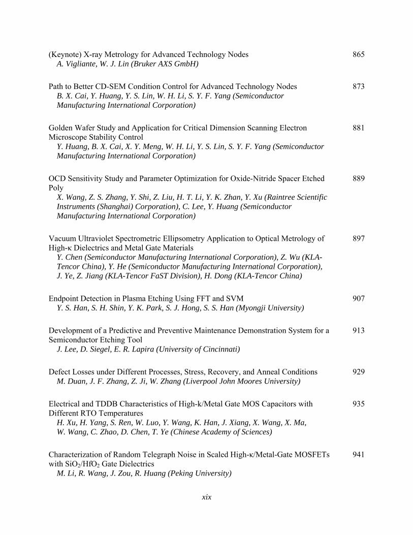
(Keynote) X-ray Metrology for Advanced Technology Nodes A. Vigliante, W. J. Lin (Bruker AXS GmbH)
865
Path to Better CD-SEM Condition Control for Advanced Technology Nodes
B. X. Cai, Y. Huang, Y. S. Lin, W. H. Li, S. Y. F. Yang (Semiconductor Manufacturing International Corporation)
873
Golden Wafer Study and Application for Critical Dimension Scanning Electron Microscope Stability Control
Y. Huang, B. X. Cai, X. Y. Meng, W. H. Li, Y. S. Lin, S. Y. F. Yang (Semiconductor Manufacturing International Corporation)
881
OCD Sensitivity Study and Parameter Optimization for Oxide-Nitride Spacer Etched Poly
X. Wang, Z. S. Zhang, Y. Shi, Z. Liu, H. T. Li, Y. K. Zhan, Y. Xu (Raintree Scientific Instruments (Shanghai) Corporation), C. Lee, Y. Huang (Semiconductor Manufacturing International Corporation)
889
Vacuum Ultraviolet Spectrometric Ellipsometry Application to Optical Metrology of High-κ Dielectrics and Metal Gate Materials
Y. Chen (Semiconductor Manufacturing International Corporation), Z. Wu (KLA-Tencor China), Y. He (Semiconductor Manufacturing International Corporation), J. Ye, Z. Jiang (KLA-Tencor FaST Division), H. Dong (KLA-Tencor China)
897
Endpoint Detection in Plasma Etching Using FFT and SVM
Y. S. Han, S. H. Shin, Y. K. Park, S. J. Hong, S. S. Han (Myongji University) 907
Development of a Predictive and Preventive Maintenance Demonstration System for a Semiconductor Etching Tool
J. Lee, D. Siegel, E. R. Lapira (University of Cincinnati)
913
Defect Losses under Different Processes, Stress, Recovery, and Anneal Conditions
M. Duan, J. F. Zhang, Z. Ji, W. Zhang (Liverpool John Moores University) 929
Electrical and TDDB Characteristics of High-k/Metal Gate MOS Capacitors with Different RTO Temperatures
H. Xu, H. Yang, S. Ren, W. Luo, Y. Wang, K. Han, J. Xiang, X. Wang, X. Ma, W. Wang, C. Zhao, D. Chen, T. Ye (Chinese Academy of Sciences)
935
Characterization of Random Telegraph Noise in Scaled High-κ/Metal-Gate MOSFETs with SiO2/HfO2 Gate Dielectrics
M. Li, R. Wang, J. Zou, R. Huang (Peking University)
941

xx
The Failure Mechanism Worst Stress Condition for Hot Carrier Injection of NMOS
Z. Song (Semiconductor Manufacturing International (Shanghai) Corp.), Z. Chen (Sandisk Infromation Technology (Shanghai) Co. Ltd.), A. Z. Yong, Y. Song, J. Wu, K. Chien (Semiconductor Manufacturing International (Shanghai) Corp.)
947
Negative Bias Temperature Instability Characteristics and Degradation Mechanisms of pMOSFET with High-k/Metal Gate Stacks
S. Ren, H. Yang, W. Wang, H. Xu, W. Luo, B. Tang, Z. Tang, J. Xu, J. Yan, C. Zhao, T. Ye (Chinese Academy of Sciences)
953
Effect of Low-Temperature on Endurance Characteristics of SONOS Memory
L. Liu (East China Normal University), G. Shen, G. Cao (Shanghai Hua Hong NEC Electronics Company Ltd.), S. Zhang, Y. Shi (East China Normal University)
959
Chapter 9 Emerging Semiconductor Technologies
Process Optimization of HfAlO Trapping Layer for High Performance Charge Trap Flash Memory Application
D. Zhang, Z. Huo, X. Yang, Z. Liu, G. Chen, Y. Han, Z. Sun, Y. Chu, C. Wang (Chinese Academy of Sciences), B. Yang (Tianjin University of Technology), M. Liu (Chinese Academy of Sciences)
967
Resistance Switching Properties of Titanium Oxide with Different Copper Electrode Structure
X. Shao, J. Zhao, K. Zhang, R. Chen, L. Zhou, C. Chen, J. Wang (Tianjin University of Technology)
973
(Invited) Technological Approaches Towards High Voltage, Fast Switching GaN Power Transistors
J. Würfl, O. Hilt, E. Bahat-Treidel, R. Zhytnytska, K. Klein, P. Kotara, F. Brunner, A. Knauer, O. Krüger, M. Weyers, G. Tränkle (Ferdinand-Braun-Institut)
979
(Invited) Instability Assessment and Modeling Of Amorphous InGaZnO Thin Film Transistors Under Alternating Pulse Bias Stresses
S. Park, E. N. Cho, I. Yun (Yonsei University)
991

xxi
Electrical Properties and Conduction Mechanism of RRAM With Al/WOX/Cu Structure
L. Tao, Z. Kailiang, W. Fang, S. Kuo, S. Wenxiang, Z. Jinshi (Tianjin University of Technology)
1003
Resistive Switching Characteristics of Zinc Oxide Resistive RAM Doped with Nickel
S. Wenxiang, Z. Kailiang, W. Fang, S. Kuo, M. Yinping, Z. Jinshi (Tianjin University of Technology)
1009
Synthesis of Zinc Oxide Nanowires by Cu-Additive Zinc Acetate Solution with Hydrothermal Method
Y. Wang, Y. Lai, S. Cheng (Fuzhou University)
1015
The Optimization of Thermal Flow Field in a Large-Size MOCVD Reactor
C. K. Hu Jr., T. T. Li, Y. J. Lin (National Central University) 1021
Graphene-Based Inductors: Fabrication and Performance
M. Zhou, L. Ren, Z. Wei, H. B. Zhao, B. Hu, Y. Jia, Z. Shi, Y. Fu, R. Huang, X. Zhang (Peking University)
1027
Gate-Modulated Photoresponse in Graphene Field-Effect Transistors
Z. Wei, Z. Wang, H. Zhao, T. Ye, L. Ren, J. Guo, Y. Jia, Z. Zhang, Y. Fu, R. Huang, X. Zhang (Peking University)
1033
Chapter 10 Advances in MEMS and Sensor Technologies
(Keynote) Smart Systems for a Better Life
T. Gessner, M. Vogel (Fraunhofer Institute for Electronic Nano Systems), J. Nestler, K. Hiller (Chemnitz University of Technology), S. Kurth, T. Otto (Fraunhofer Institute for Electronic Nano Systems)
1041
(Keynote) Solid-State Nanopore Fabrication with Conventional Process
Z. Liu, T. Deng (Tsinghua University), J. Chen (Guizhou University) 1047
(Keynote) Chinas Markets - No Option for German SMEs
H. P. Hippler (HIPPLER International Business Development & Education) 1053
(Keynote) PowerMEMS Based on Semiconductor Technologies and Nano Materials
X. Wang, C. Shen, H. Xing (Tsinghua University) 1059
xxii
(Invited) Equivalent Circuit Representation of Resonant Accelerometer
Y. Jia, Y. Hao (Peking University), Q. Huang (The 5th Electronics Research Institute of the Ministry of Industry and Information Technology)
1065
(Invited) Direct Electrochemical Detection of ssDNA with a Micro Three-Electrode System
T. Deng, C. X. Zhao (Institute of Microelectronics, Tsinghua University), M. W. Li (National Key Laboratory for Electronic Measurement Technology, North University of China), Z. W. Liu (Institute of Microelectronics, Tsinghua University)
1071
Chapter 11 Circuit Design, System Integration and Applications
(Invited) Robust Subthreshold Circuit Design to Manufacturing and Environmental Variability
M. Hashimoto (Osaka University)
1079
Unified Automated System Level Test Bench to Verify DDR2/3/4 and LPDDR2 Memory Controllers - Layered
J. N. Raghavendra (XILINX)
1085
An Optimization Procedure for Coil Design in a Dual Band Wireless Power and Data Transmission System
W. Li, H. Yuan, W. Xu (Shanghai Jiao Tong University), K. Geng (University of Southern California), G. Wang (Shanghai Jiao Tong University)
1091
A CMOS Potentiostat Circuit for Parallel Direct DNA Sensing
T. Dai (Guizhou University), L. Zhang, M. Li (Tsinghua University), C. Wu (Guizhou University), Z. Liu (Tsinghua University)
1099
Author Index 1105

Facts about ECSThe Electrochemical Society (ECS) is an international, nonprofi t, scientifi c, educational organization founded for the advancement of the theory and practice of electrochemistry, electronics, and allied subjects. The Society was founded in Philadelphia in 1902 and incorporated in 1930. There are currently over 7,000 scientists and engineers from more than 70 countries who hold individual membership; the Society is also supported by more than 100 corporations through Corporate Memberships.
The technical activities of the Society are carried on by Divisions. Sections of the Society have been organized in a number of cities and regions. Major international meetings of the Society are held in the spring and fall of each year. At these meetings, the Divisions and Groups hold general sessions and sponsor symposia on specialized subjects.
The Society has an active publication program that includes the following:
Journal of The Electrochemical Society — (JES) is the leader in the fi eld of electrochemical science and technology. This peer-reviewed journal publishes an average of 550 pages of 85 articles each month. Articles are published online as soon as possible after undergoing the peer-review process. The online version is considered the fi nal version and is fully citable with articles assigned specifi c page numbers within specifi c issues. The date of online publication is the offi cial publication date of record.
Journal of Solid State Science and Technology — (JSS) is one of the newest peer-reviewed journals from ECS launched in 2012. JSS covers fundamental and applied areas of solid state science and technology including experimental and theoretical aspects of the chemistry and physics of materials and devices. Articles are published online as soon as possible after undergoing the peer-review process. The online version is considered the fi nal version and is fully citable with articles assigned specifi c page numbers within specifi c issues. The date of online publication is the offi cial publication date of record.
Electrochemistry Letters — (EEL) is one of the newest journals from ECS launched in 2012. It is dedicated to the rapid dissemination of peer-reviewed and concise research reports in fundamental and applied areas of electrochemical science and technology. Articles are published online as soon as possible after undergoing the peer-review process. The online version is considered the fi nal version and is fully citable with articles assigned specifi c page numbers within specifi c issues. The date of online publication is the offi cial publication date of record.
Solid State Letters — (SSL) is one of the newest journals from ECS launched in 2012. It is dedicated to the rapid dissemination of peer-reviewed and concise research reports in fundamental and applied areas of solid state science and technology. Articles are published online as soon as possible after undergoing the peer-review process. The online version is considered the fi nal version and is fully citable with articles assigned specifi c page numbers within specifi c issues. The date of online publication is the offi cial publication date of record.
Electrochemical and Solid-State Letters — (ESL) was the fi rst rapid-publication electronic journal dedicated to covering the leading edge of research and development in the fi eld of solid-state and electrochemical science and technology. ESL was a joint publication of ECS and IEEE Electron Devices Society. Volume 1 began July 1998 and contained six issues, thereafter new volumes began with the January issue and contained 12 issues. The fi nal issue of ESL was Volume 16, Number 6, 2012. Preserved as an archive, ESL has since been replaced by SSL and EEL.
Interface— Interface is an authoritative yet accessible publication for those in the fi eld of solid-state and electrochemical science and technology. Published quarterly, this four-color magazine contains technical articles about the latest developments in the fi eld, and presents news and information about and for members of ECS.
ECS Meeting Abstracts— ECS Meeting Abstracts contain extended abstracts of the technical papers presented at the ECS biannual meetings and ECS-sponsored meetings. This publication offers a fi rst look into the current research in the fi eld. ECS Meeting Abstracts are freely available to all visitors to the ECS Digital Library.
ECS Transactions— (ECST) is the online database containing full-text content of proceedings from ECS meetings and ECS-sponsored meetings. ECST is a high-quality venue for authors and an excellent resource for researchers. The papers appearing in ECST are reviewed to ensure that submissions meet generally-accepted scientifi c standards. Each meeting is represented by a volume and each symposium by an issue.
Monograph Volumes — The Society sponsors the publication of hardbound monograph volumes, which provide authoritative accounts of specifi c topics in electrochemistry, solid-state science, and related disciplines.
For more information on these and other Society activities, visit the ECS website:
www.electrochem.org