Embed Size (px)
Citation preview
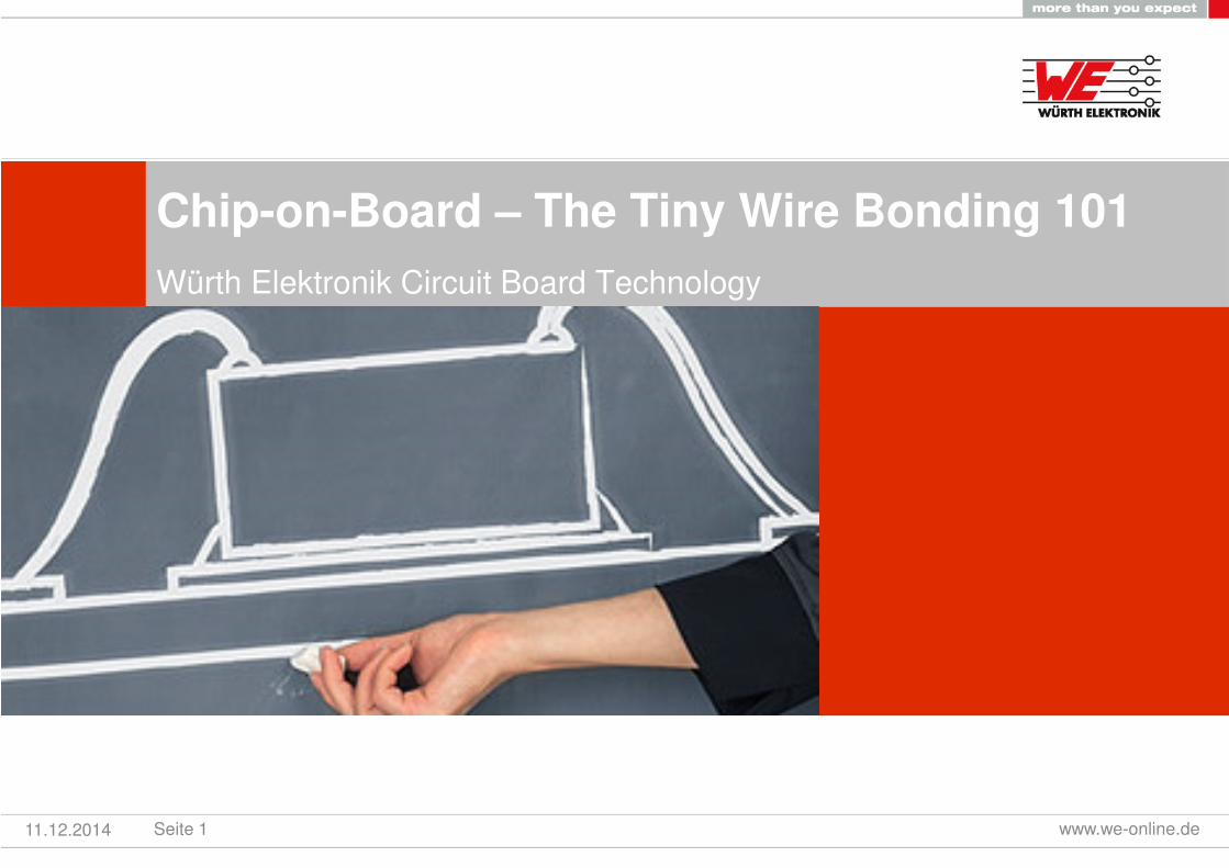
Chip-on-Board – The Tiny Wire Bonding 101
Würth Elektronik Circuit Board Technology
11.12.2014 Seite 1 www.we-online.de
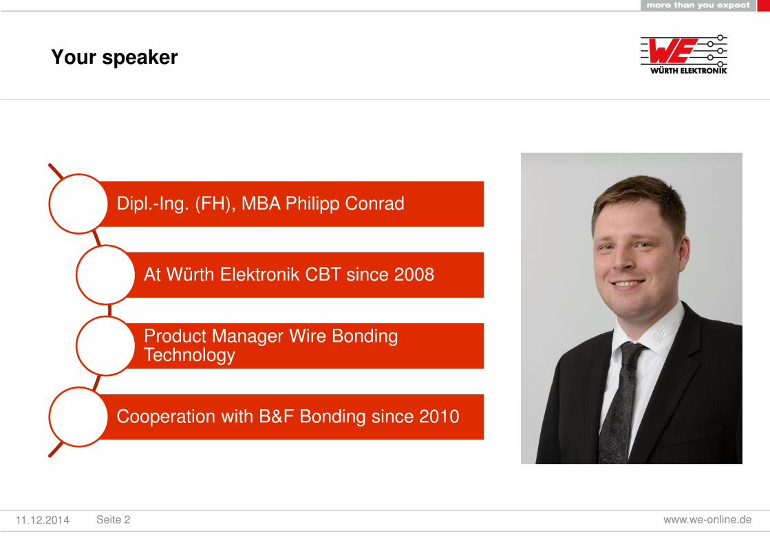
Your speaker
www.we-online.deSeite 211.12.2014
Dipl.-Ing. (FH), MBA Philipp Conrad
At Würth Elektronik CBT since 2008
Product Manager Wire BondingTechnology
Cooperation with B&F Bonding since 2010
Agenda
Chip / Bare Die
Gold und Aluminium Wire Bonding
PCB Design
Protection of Die and Wirebonds
www.we-online.deSeite 311.12.2014
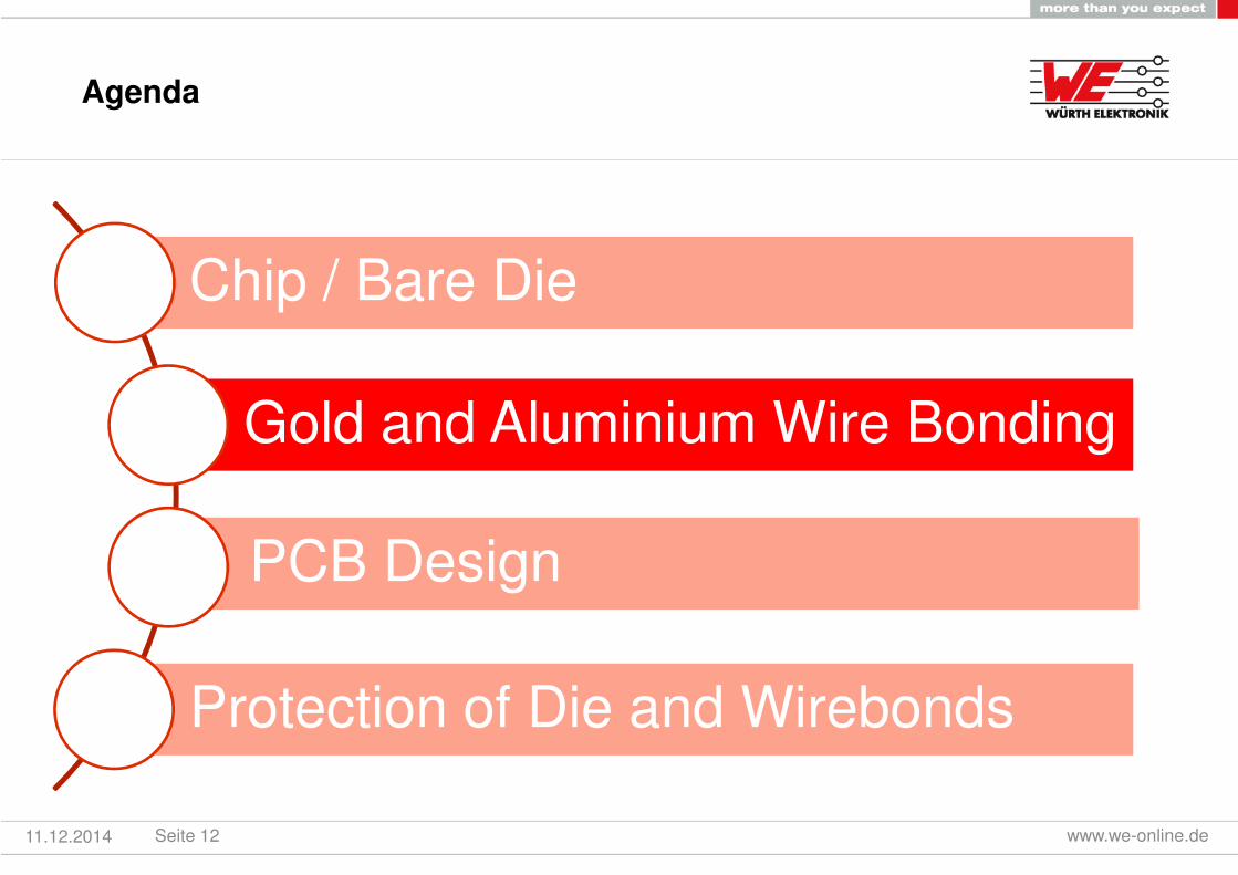
Agenda
Chip / Bare Die
Gold and Aluminium Wire Bonding
PCB Design
Protection of Die and Wirebonds
www.we-online.deSeite 411.12.2014

Comparison: Housed Chip / Bare Die
11.12.2014 Seite 5 www.we-online.de
Substrate
QFP
Wire bonding on a Substrate
Substrate
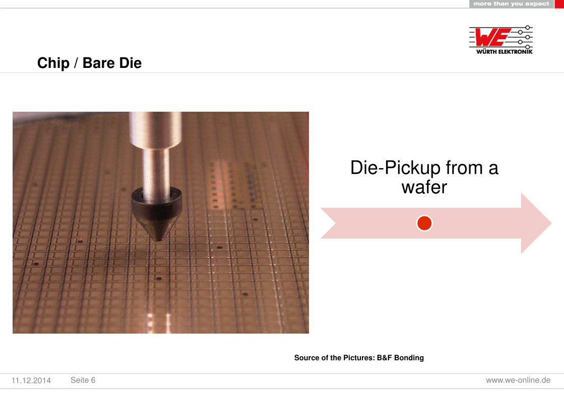
Chip / Bare Die
11.12.2014 Seite 6 www.we-online.de
Source of the Pictures: B&F Bonding
Die-Pickup from a wafer
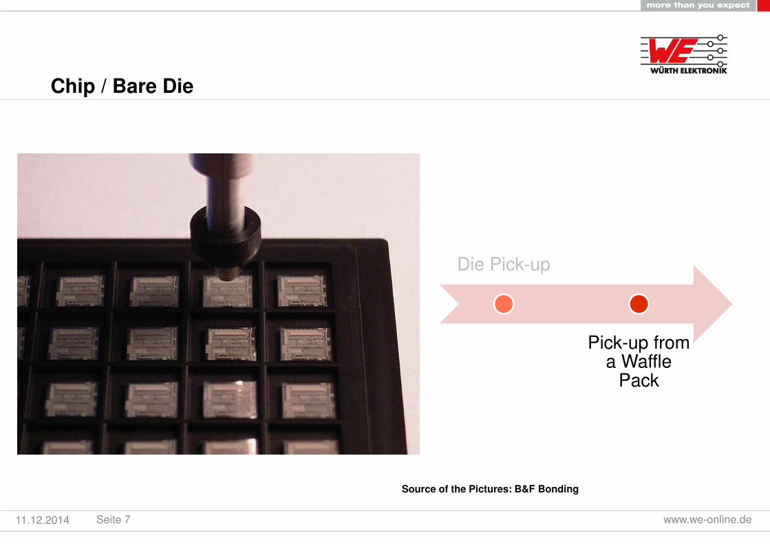
Chip / Bare Die
11.12.2014 Seite 7 www.we-online.de
Source of the Pictures: B&F Bonding
Die Pick-up
Pick-up froma Waffle
Pack
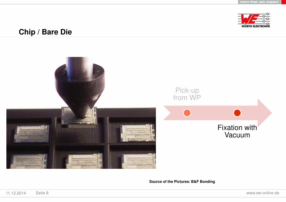
Chip / Bare Die
11.12.2014 Seite 8 www.we-online.de
Source of the Pictures: B&F Bonding
Pick-up from WP
Fixation withVacuum
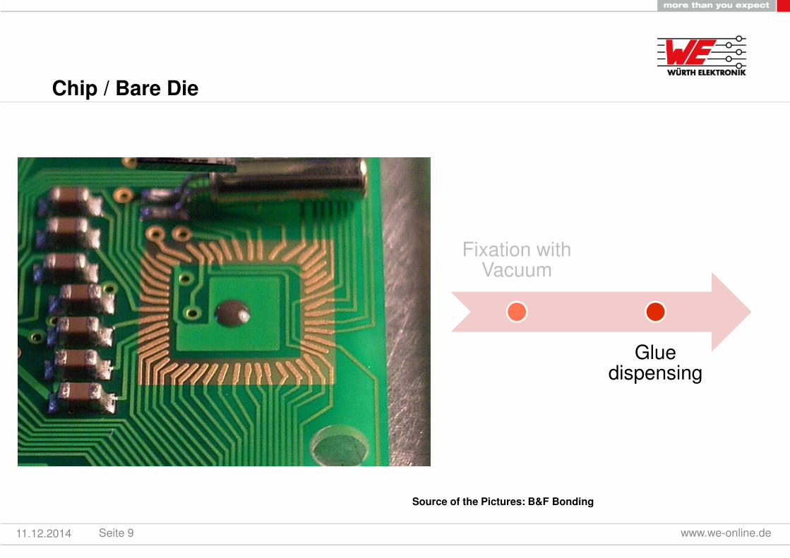
Chip / Bare Die
11.12.2014 Seite 9 www.we-online.de
Source of the Pictures: B&F Bonding
Fixation withVacuum
Gluedispensing
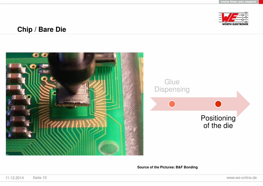
Chip / Bare Die
11.12.2014 Seite 10 www.we-online.de
Source of the Pictures: B&F Bonding
GlueDispensing
Positioningof the die
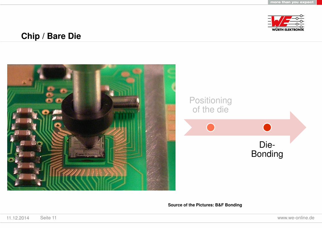
Chip / Bare Die
11.12.2014 Seite 11 www.we-online.de
Source of the Pictures: B&F Bonding
Positioningof the die
Die-Bonding
Agenda
Chip / Bare Die
Gold and Aluminium Wire Bonding
PCB Design
Protection of Die and Wirebonds
www.we-online.deSeite 1211.12.2014
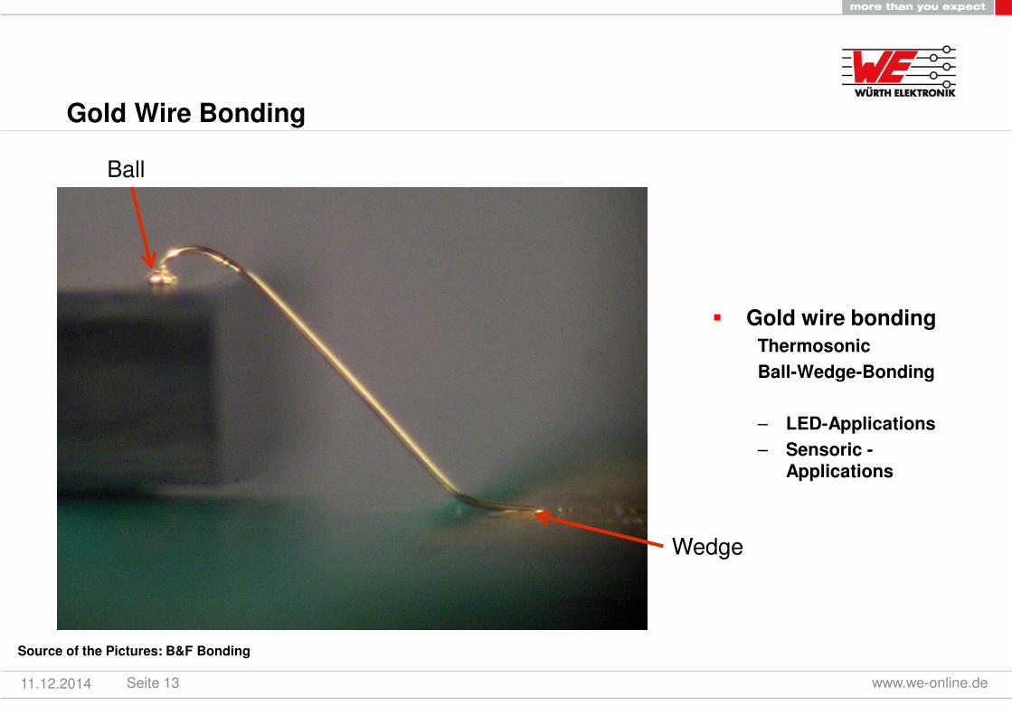
Gold Wire Bonding
� Gold wire bonding
Thermosonic
Ball-Wedge-Bonding
– LED-Applications
– Sensoric -Applications
11.12.2014 Seite 13 www.we-online.de
Source of the Pictures: B&F Bonding
Ball
Wedge
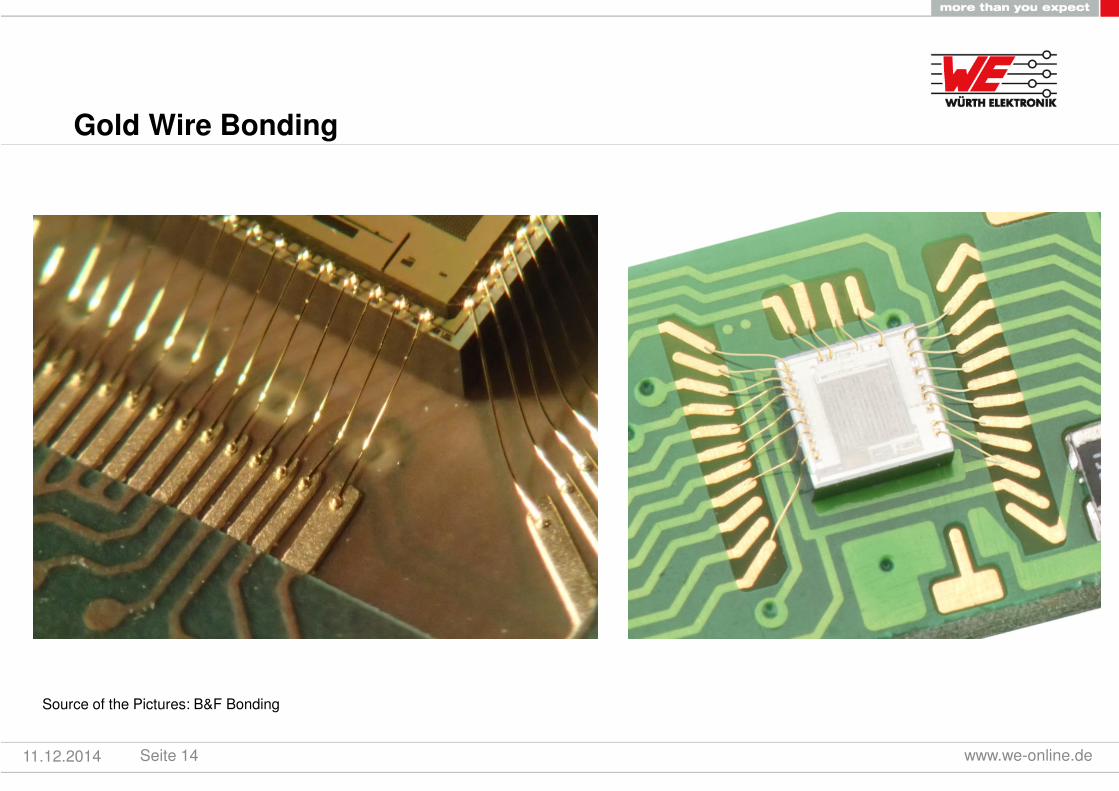
Gold Wire Bonding
11.12.2014 Seite 14 www.we-online.de
Source of the Pictures: B&F Bonding
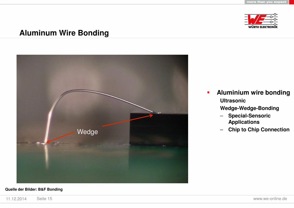
Aluminum Wire Bonding
11.12.2014 Seite 15 www.we-online.de
� Aluminium wire bonding
Ultrasonic
Wedge-Wedge-Bonding
– Special-SensoricApplications
– Chip to Chip Connection
Quelle der Bilder: B&F Bonding
Wedge
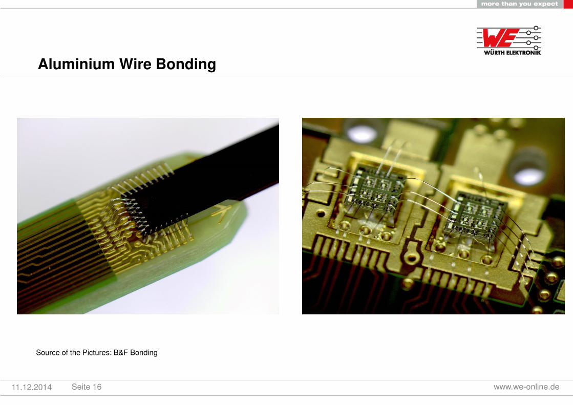
Aluminium Wire Bonding
11.12.2014 Seite 16 www.we-online.de
Source of the Pictures: B&F Bonding
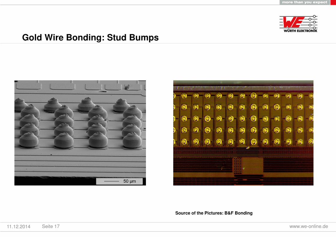
Gold Wire Bonding: Stud Bumps
11.12.2014 Seite 17 www.we-online.de
Source of the Pictures: B&F Bonding
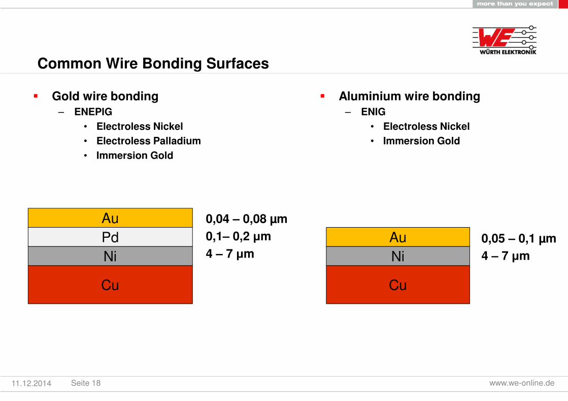
Common Wire Bonding Surfaces
� Gold wire bonding
– ENEPIG
• Electroless Nickel
• Electroless Palladium
• Immersion Gold
11.12.2014 Seite 18 www.we-online.de
Cu
NiPd
0,04 – 0,08 µm
0,1– 0,2 µm
4 – 7 µm
Au
Cu
NiAu 0,05 – 0,1 µm
4 – 7 µm
� Aluminium wire bonding
– ENIG
• Electroless Nickel
• Immersion Gold
Agenda
Chip / Bare Die
Gold and Aluminium Wire Bonding
PCB Design
Protection of Die and Wirebonds
www.we-online.deSeite 1911.12.2014
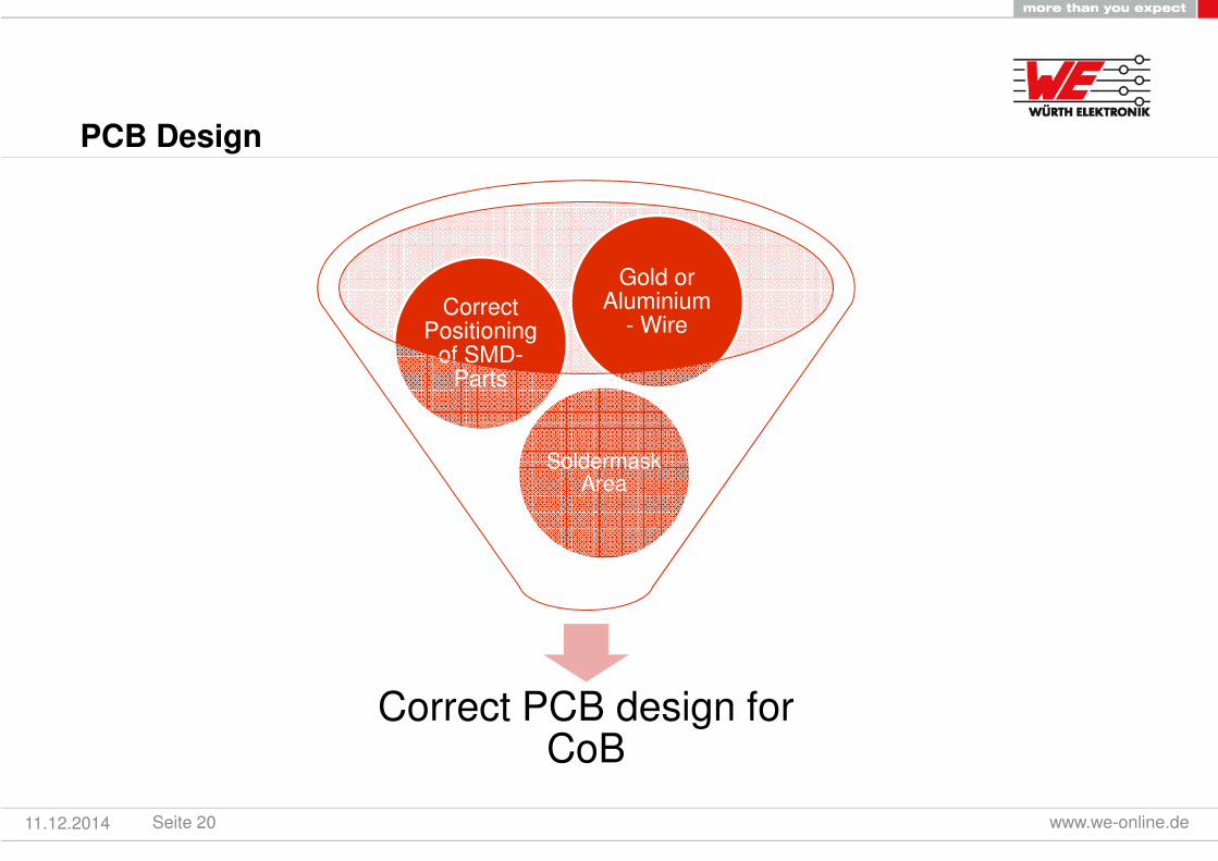
PCB Design
11.12.2014 Seite 20 www.we-online.de
Correct PCB design forCoB
SoldermaskArea
CorrectPositioning
of SMD-Parts
Gold orAluminium
- Wire
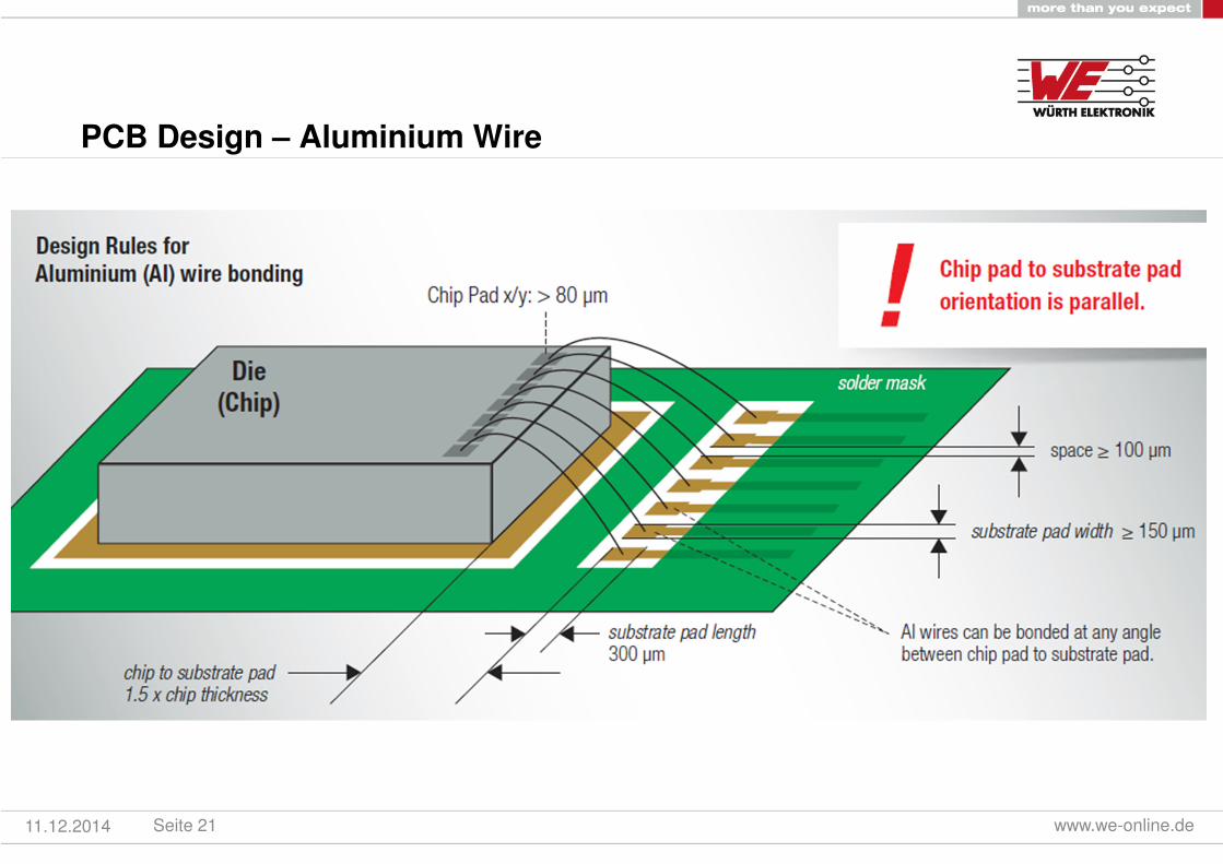
PCB Design – Aluminium Wire
11.12.2014 Seite 21 www.we-online.de
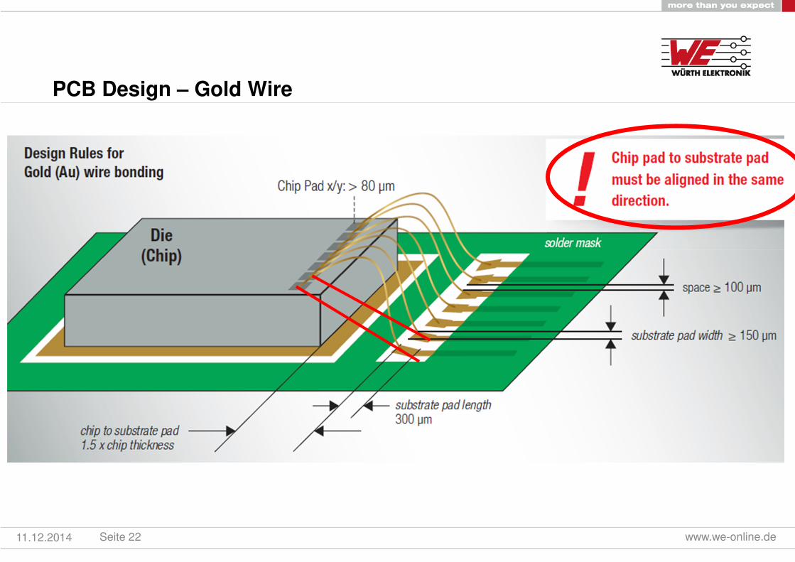
PCB Design – Gold Wire
11.12.2014 Seite 22 www.we-online.de
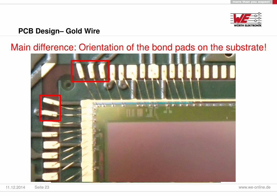
PCB Design– Gold Wire
11.12.2014 Seite 23 www.we-online.de
Main difference: Orientation of the bond pads on the substrate!
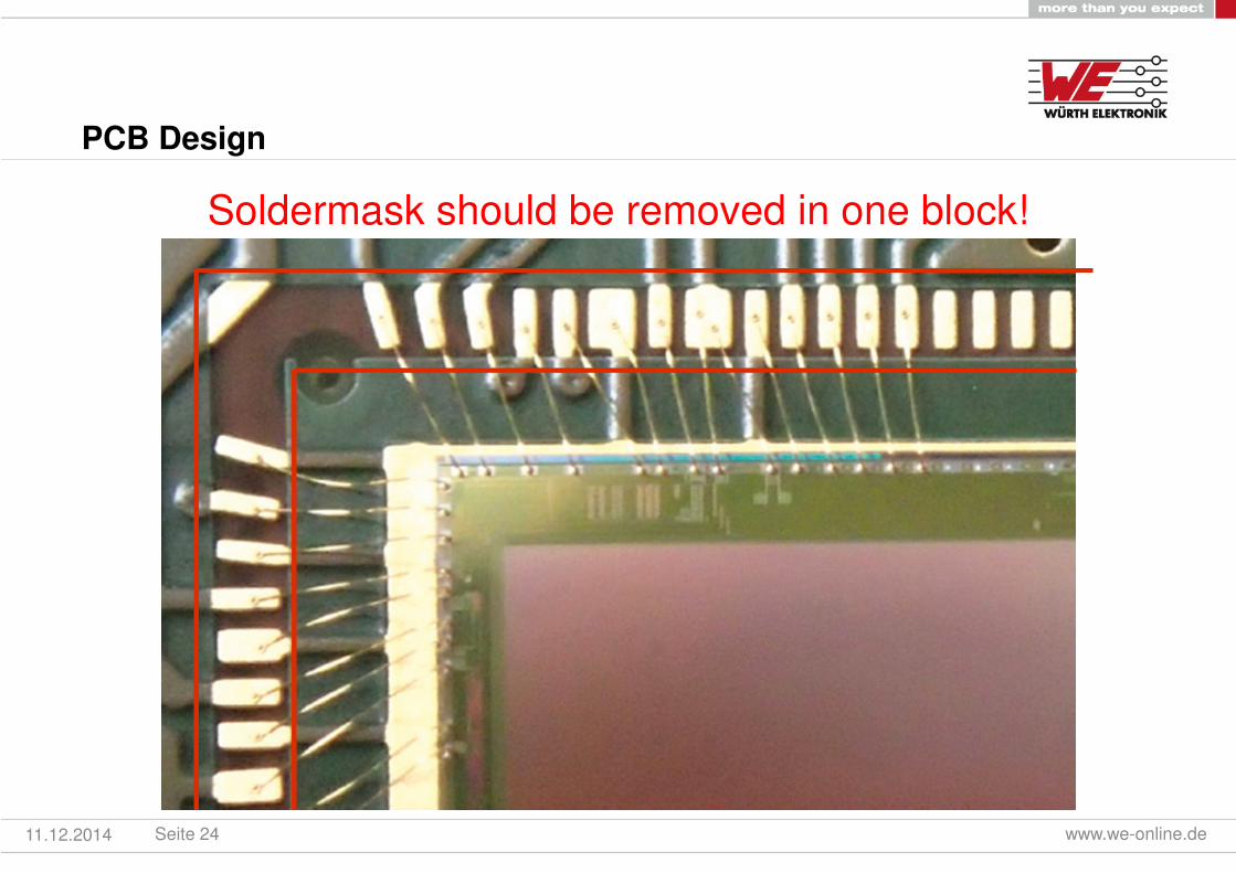
PCB Design
11.12.2014 Seite 24 www.we-online.de
Soldermask should be removed in one block!
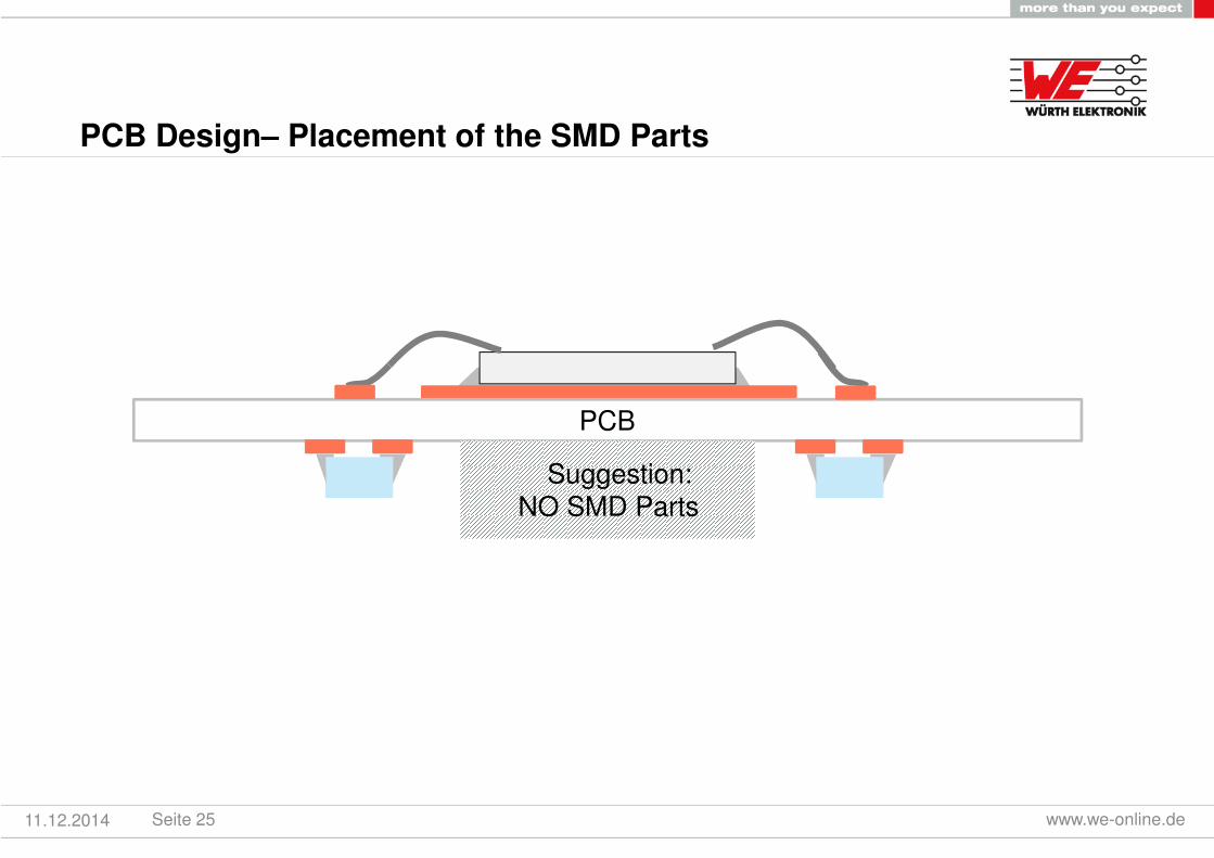
PCB Design– Placement of the SMD Parts
11.12.2014 Seite 25 www.we-online.de
PCB
Suggestion:NO SMD Parts
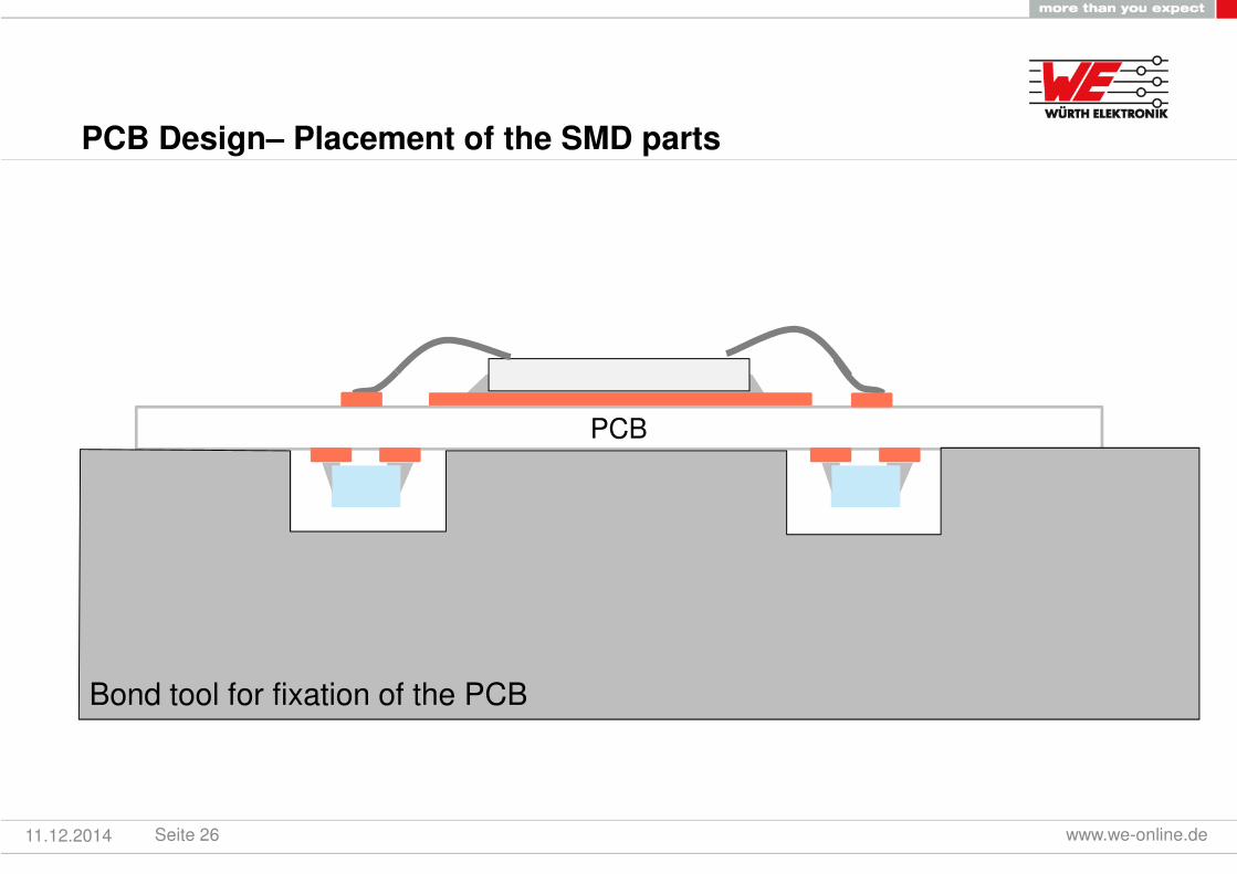
PCB Design– Placement of the SMD parts
11.12.2014 Seite 26 www.we-online.de
PCB
Bond tool for fixation of the PCB
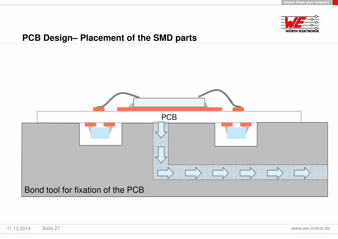
PCB Design– Placement of the SMD parts
11.12.2014 Seite 27 www.we-online.de
PCB
Bond tool for fixation of the PCB
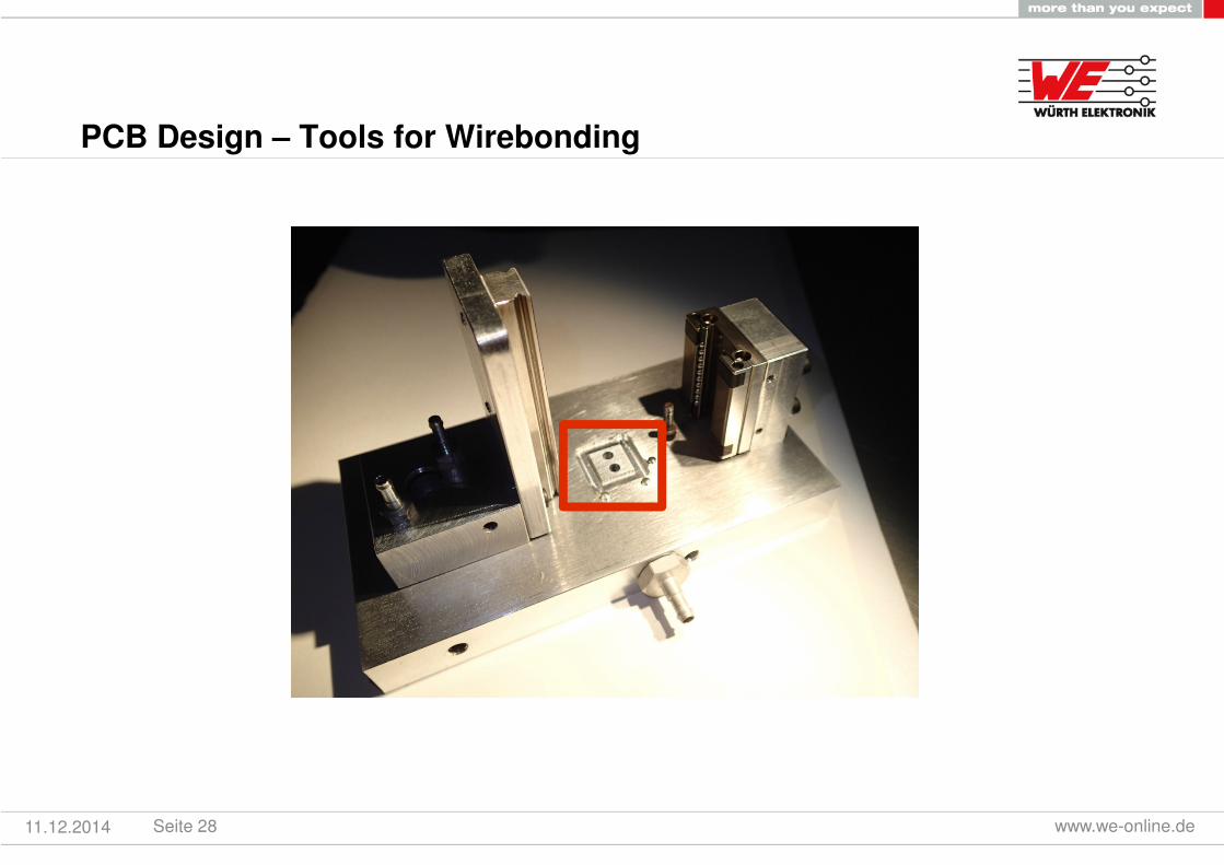
PCB Design – Tools for Wirebonding
11.12.2014 Seite 28 www.we-online.de
Agenda
Chip / Bare Die
Gold und Aluminium Wire Bonding
PCB Design
Protection of Die and Wirebonds
www.we-online.deSeite 2911.12.2014
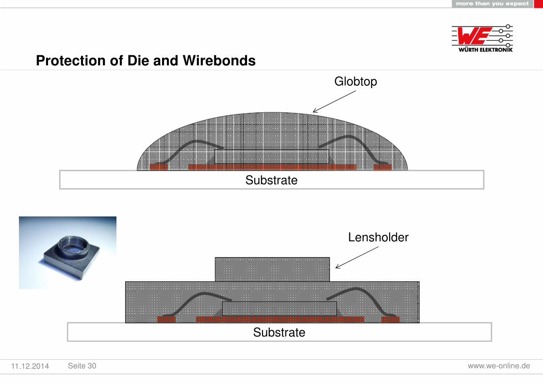
Substrate
Protection of Die and Wirebonds
11.12.2014 Seite 30 www.we-online.de
Substrate
Globtop
Lensholder
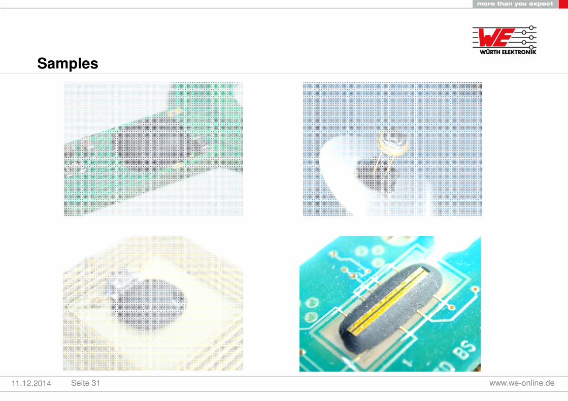
Samples
11.12.2014 Seite 31 www.we-online.de
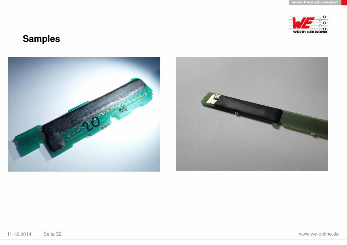
Samples
11.12.2014 Seite 32 www.we-online.de
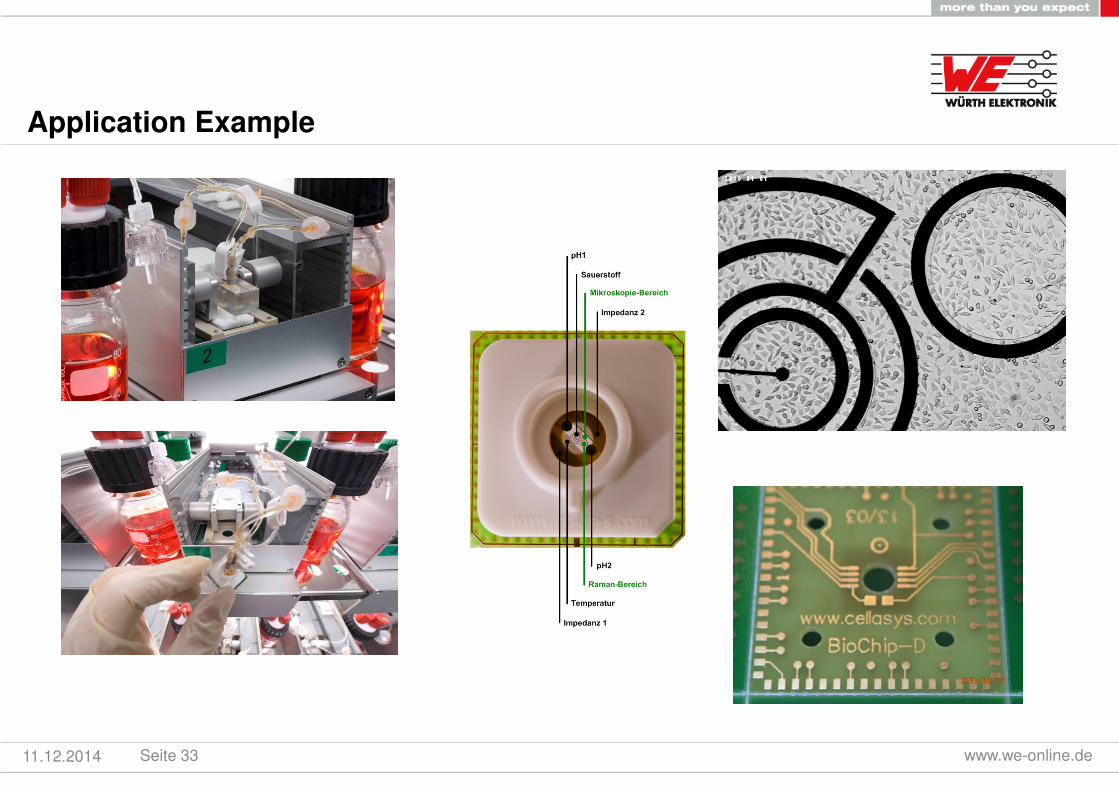
Application Example
www.we-online.deSeite 3311.12.2014
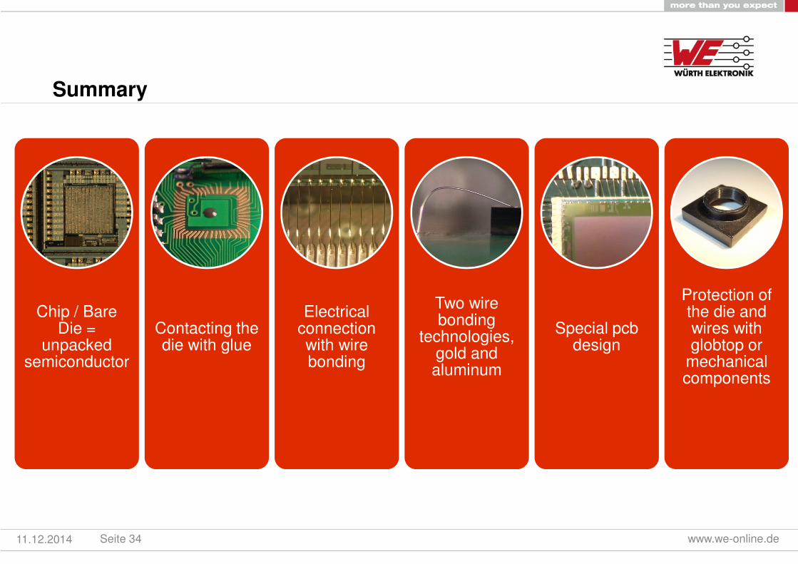
Summary
11.12.2014 Seite 34 www.we-online.de
Chip / Bare Die =
unpackedsemiconductor
Contacting thedie with glue
Electricalconnectionwith wirebonding
Two wirebonding
technologies, gold andaluminum
Special pcbdesign
Protection ofthe die andwires withglobtop or
mechanicalcomponents
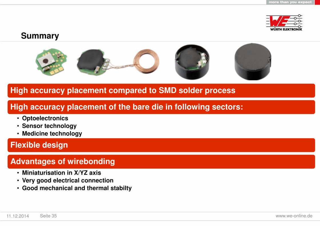
Summary
High accuracy placement compared to SMD solder process
High accuracy placement of the bare die in following sectors:
• Optoelectronics
• Sensor technology
• Medicine technology
Flexible design
Advantages of wirebonding
• Miniaturisation in X/YZ axis
• Very good electrical connection
• Good mechanical and thermal stabilty
11.12.2014 Seite 35 www.we-online.de

11.12.2014 Seite 36 www.we-online.de
Thanks for your attention!
Philipp ConradWÜRTH ELEKTRONIK GmbH & Co. KGProcukt Management Wire bondingCircuit Board TechnologyM.:+49 175 2271 600E. [email protected]. www.we-online.de


![Dnevni avaz [broj 6947 djelimičan, 11.12.2014]](https://img.pdfslide.net/doc/110x75/577cc19d1a28aba71193772e/dnevni-avaz-broj-6947-djelimican-11122014.jpg)