Embed Size (px)
Citation preview

Circuit Design for Linearizing Transmitter
Sim Chan Kuen
NATIONAL UNIVERSITY OF SINGAPORE
2003

Circuit Design for Linearizing Transmitter
Sim Chan Kuen, (B. Eng., Nanyang Technological University)
DEPARTMENT OF ELECTRICAL ENGINEERING
A THESIS SUBMITTED
FOR THE DEGREE OF MASTER OF ENGINEERING
NATIONAL UNIVERSITY OF SINGAPORE
2003

i
Acknowledgement I would like to take this opportunity to express my warmest thanks to many people
who have contributed towards the production of this thesis.
In particular, I thank my supervisors, Dr. Michael Chia Y. W. and Prof. Lye Kin Mun.
I thank Dr. Michael Chia for his guidance and support. He spent a tremendous amount
of time teaching me discussing the research problem and checking this thesis.
I thank my friends and colleagues in the Transceiver System group of Institute of
Infocomm Research (I2R). They advised me throughout the course of work and in
completion of this thesis.
Lastly, I thank my family for their constant support and care.

ii
Contents
Acknowledgement i
Contents ii
List of Figures v
List of Tables viii
Summary ix
Chapter 1 Introduction 1
1.1 Background 1
1.2 Power Amplifier 3
1.3 Objective 5
1.4 Thesis Organization 5
Chapter 2 Power Amplifier Characteristics and Linearization 7
2.1 Classification of Power amplifier 7
2.2 Distortions of Power Amplifier 9
2.3 Modeling of Power Amplifier 13
2.4 Power Amplifier Testing 14
2.4.1 Two Tones Test 14
2.4.2 Noise-Power-Ratio (NPR) 15
2.4.3 Adjacent Channel Power Rejection (ACPR) 15
2.4.4 Emission Mask 16
2.5 Linearization 17
2.5.1 Cartesian Feedback 17
2.5.2 Feedforward 19

iii
2.5.3 Envelope Elimination and Restoration 21
2.5.4 Linear Amplification with Non-Linear Components 22
2.5.5 Predistortion 24
Chapter 3 The Design of Analog Predistorter 27
3.1 Introduction 28
3.2 System block of the analog predistorter 32
3.3 System Consideration 35
3.4 Circuit Implementation 39
3.4.1 Analog Multiplier 39
3.4.1.1 Brief Survey 39
3.4.1.2 Implementation of Analog Multiplier 43
3.4.2 Transconductance cell 50
3.4.3 Transimpedance cell and Output Buffer 52
3.5 Simulation 54
3.6 Layout 56
3.7 Completed Chip 59
Chapter 4 Tests Results for the Analog Predistorter 60
4.1 Predistorter Performance 61
4.2 Low-IF Analog predistortion 62
4.2.1 Two-Tone Tests 62
4.2.2 Multi-carrier signals 68
4.2.3 OFDM signals 70
4.2.4 IS95 73
4.3 Baseband analog predistortion 75

iv
4.4 Analog predistortion for Radio Over Fiber System (ROF) 80
Chapter 5 Conclusions 87
Bibliography 90
Appendix 95

v
List of Figures 1.1 Modern Transmitter Architecture 2
2.1 Basic Circuit Diagram for Power Amplifier 8
2.2 Power Amplifier characteristics 11
2.3 Intermodulation Distortion of Power Amplifier 11
2.4 Noise Power Ratio Testing 15
2.5 ACPR 15
2.6 Emission Mask 16
2.7 Cartesian Feedback 18
2.8 Feedforward Linearization 19
2.9 Envelope Elimination and Restoration 21
2.10 Linear Amplification with Non-Linear Components 22
2.11 Basic principle of Predistortion 24
3.1 Implementation of Predistorter at different stage of the Transmitter 31
3.2 Block of the 3rd Order Analog Predistorter 35
3.3 A Basic Bipolar implementation of Analog Mulitplier 40
3.4 Two general method of implementing analog multiplier in CMOS 41
3.5 Analog Multiplier 44
3.6 The complete analog multiplier 47
3.7 Simulated Result of the multiplier 48
3.8 Simulated distortions in multiplier 49
3.9 Transconductance cell 51
3.10 Simulated results of the transconductance cell 52
3.11 Transimpedance cell 53

vi
3.12 Output Buffer 54
3.13 Die photo of the predistorter 59
4.1 Pout vs Pin of the power amplifier 62
4.2 A Two Tone Test performed on the power amplifier 63
4.3 Test setup for low-IF predistorter 64
4.4 Before Linearization (Two-tones test at low-IF) 65
4.5 After Linearization (Two-tones test at low-IF) 65
4.6 A two-tones test with varying input power 66
4.7 Multi-Carrier Test(Before Linearization) 68
4.8 Multi-Carrier Test(After Linearization) 69
4.9 Frequency spectrum at the input of the power amplifier
(Before Linearization) 71
4.10 Frequency spectrum at the ouptut of the power amplifier
(Before Linearization) 71
4.11 Frequency spectrum at the input of the power amplifier
(After Linearization) 72
4.12 Frequency spectrum at the output of the power amplifier
(After Linearization) 72
4.13 IS95 signals (Before Linearization) 74
4.14 IS95 signals (After Linearization) 74
4.15 Test setup of baseband predistortion 76
4.16 Overall output spectrum for baseband predistortion
two-tones test (before linearization) 77
4.17 Zooming on the frequency spectrum around the two tones
for baseband predistortion two-tones test (before linearization) 77

vii
4.18 Overall output spectrum for baseband predistortion two-tones
test (after linearization) 78
4.19 Zooming on the frequency spectrum around the two tones
for baseband predistortion two-tones test (after linearization) 78
4.20 Test Setup using predistorter in Radio Over Fiber system 80
4.21 Overall output spectrum for ROF predistortion two-tones
test (before linearization) 81
4.22 Zooming on the frequency spectrum around the two tones
for ROF predistortion two-tones test (before linearization) 81
4.23 Overall output spectrum for ROF predistortion two-tones
test (after linearization) 82
4.24 Zooming on the frequency spectrum around the two tones
for ROF predistortion two-tones test (after linearization) 82
4.25 Two-tones test for ROF system 83
4.26 Multi-Carrier Test for ROF system(Before Linearization) 85
4.27 Multi-Carrier Test for ROF system(After Linearization) 85

viii
List of Tables
4.1 Performance of Predistorter 61
4.1 Comparison of two-tone test results performed by different design 67

Chapter 1
Introduction
1.1 Background
The primary purpose of any wireless communication systems is to transmit or receive
information. The information could be in any form such as speech, pictures or data. In the
area of cellular and personal communication service (PCS) systems, there is a trend of
transmitting data and video instead of merely speech. In third generation (3G) cellular
systems, such as WCDMA system, the data rates that could be transmitted will enable
even video to be transmitted through cellular systems. With higher data rates of the 3G
systems, it will open up a whole range of services to the consumers.
One of the major enabling device for 3G or future cellular systems is the transceiver.

Page 2
It consists of the two major blocks, the receiver and transmitter. The receiver receives
information from air. Whereas the transmitter transmits information generated by the
cellular terminals to the air. It is thus front end of cellular communication systems.
I
Q
RF PowerAmplifier
Antenna
LocalOscillator
900 PhaseShifter
DAC
DAC
VGA
Figure 1.1 Modern Transmitter Architecture
The block diagram of the modern transmitter is shown in Fig 1.1 [1]. The I and Q
channels generated by the baseband is converted into analog signals by the Digital-to-
Analog converters (DAC). It will then be low pass filtered and upconverted by the mixers
to radio frequencies. The signals are amplified by the variable gain amplifiers (VGA).
The final amplification of the signals is by the power amplifier. It will drive the antenna
and transmitted to the air.

Page 3
1.2 Power Amplifier
One of the major blocks of the transmitter is the power amplifier [2]. This component
consumes the most power of the transceiver [3]. For example, RF MicroDevices’s
RF2161 [4] or Raytheon’s RTPA5250-130 [5] consume 0.4W and 0.66W respectively.
To achieve higher data rate and be spectrally efficient, communication systems use linear
modulation for example QAM (Quadrature Amplitude Modulation). Linear modulation
allows more data to be send within a given bandwidth. However, linear modulation will
have varying envelope at the output of the power amplifier. To properly amplify the
signal, the power amplifier must be linear. But linear power amplifier consumes a lot of
power compared to non-linear power amplifier.
A non-linear power amplifier will cause undesirable distortions to the transmitted signal.
This will lead to an increase in the overall error rate of the communications system. Not
only that, a non-linear power amplifier will exhibit spectral regrowth [1]. This will cause
distortions to adjacent channels.
It is possible to design a class A power amplifier to meet the linearity requirements for
modern communication systems. But class A power amplifier is highly inefficient in
power. Theoretically the efficiency of the class A amplifier is 50% [1]. But in actual
implementation, the efficiency of the power amplifier is much lower than 50%.

Page 4
Power efficiency of the power amplifier will affect the power consumption of the
transmitter. Being the most power consuming block of the transceiver, any reduction in
power consumption will reduce the power consumption of the whole transceiver system.
A reduction of power consumption will increase the talk time of the communication
equipment. This is especially important for cellular mobile phones.
Therefore there is a compromise between the efficiency and linearity of the power
amplifier. Generally, class AB power amplifier is good compromise between linearity
and efficiency.

Page 5
1.3 Objective
The objective of this research is to improve the linearity of the Radio Frequency (RF)
power amplifier so as to operate the power amplifier near the peak efficiency so as to
increase the talk time of the mobile handsets.
1.3 Thesis Organization
The thesis is organized as follows:
In chapter 2, the general characteristic of the power amplifier is explained. It shows how
the power amplifier could be modeled, the distortions it creates and the different metrices
to measure the linearity of the power amplifier. In this chapter, the reader will also
acquaints himself the general techniques that are used to improve the linearity of the
power amplifier namely feedback, feedforward and predistortion.
The next chapter, chapter 3, the design of the new analog predistorter is described. This
shall include the architecture and circuit.
In chapter 4, the chip was used to linearise an actual RF power amplifier. The chip was
tested at IF and baseband. Two-tone test was used to test the improvement in the linearity
of the power amplifier. Then different linear modulations were injected into predistorter.

Page 6
The use of the predistorter was then extended to a Radio Over Fiber (ROF) system. The
result for the new usage of the predistorter was also illustrated.
Finally, chapter 5 presents a summary of the work done in linearization of the power
amplifier.

Chapter 2
Power Amplifier Characteristics
and Linearization
In this chapter, the different classes of power amplifier, the characteristics and the
distortions caused by the power amplifier would be briefly discussed. The modeling of
the power amplifier will also be covered. Some of the existing methods of linearizing the
power amplifier will be presented.
2.1 Classification of Power amplifier
There are different classes or types of power amplifiers namely Class A, B, C, E and F.
The above different classes could be grouped into two [3]. The first group, class A, B and
C, are power amplifiers that use the transistors as current sources. The second group,
class E and F, use transistors as switches.
Page 8
RFCDC
Vin
Filtering/MatchingNetwork
RL
Figure 2.1 Basic Circuit Diagram for Power Amplifier
Figure 2.1 shows the basic circuit diagram for all the power amplifiers [1]. The radio
frequency choke (RFC) feeds the DC power to the drain of the BJT. It is to provide low
impedance for the bias but high impedance for a.c. signals. The BJT could also be
replaced by other types of transistor e.g. NMOS. Filters and matching network are
connected at the output of the power amplifier. The filtering network is to reject all
undesired out of band signals. The matching network is required to deliver sufficient
power to the load, RL.
In the first group, class A, B and C, the transistors act as current sources. The transistor
will either sink or source current to the load. The differences between class A, B and C is
in their conduction angles. In class A, the power amplifier is biased such that the current
will conduct at all times. But the conduction angle is 180 degrees and below 180 degrees

Page 9
for class B and C power amplifiers respectively. The linearity for class A power
amplifiers is the best followed by B and C. But the power efficiency is the lowest for
class A and highest for class C. A compromise between linearity and power efficiency is
met by class AB power amplifiers.
Class E [6] and F power amplifiers are non-linear power amplifiers. The transistors in
Class E power amplifiers act as a switch rather than a current source. In an ideal switch,
when it is ON, the voltage across the switch is zero and the current will be the maximum.
When the switch is OFF, the voltage should rise to the maximum while the current is
zero. Therefore the ideal switching power amplifier has 100% efficiency. In Class F
amplifier, the filtering/matching network has resonances at one or more harmonic
frequencies including the fundamental carrier frequency. The filtering/matching network
will shape the output collector voltage of the power amplifier to a square wave like
waveform [7]. Generally, Class E and F power amplifiers are more efficient compared to
Class A to C power amplifiers. However, they generate more distortions than Class A to
C power amplifiers.
2.2 Distortions of Power Amplifier
Amplitude Distortion
Ideally the output of the power amplifier should follow the equation as shown in (2.1).
The output power, Pout, is K times of the input power, Pin. K is a fix constant.
inout PKP *= --------- (2.1)
Page 10
Figure 2.2 compares the ideal response at the output of the power amplifier and the
practical amplifier. In pratice, there is a limited range where the power amplifier is able
to amplify the signal presented in the input. The value of the K, as in (2.1), changes as the
input of the power amplifier increases. When input power exceeds a certain level, the
power amplifier will be saturated. The non-linearity of the input and output of the power
amplifier is also termed as AM-AM conversion. However, the efficiency near the
saturation point is the highest.
One of the ways to compare the linearity of different amplifiers is find the P1dB point.
This is the point where the output power of the actual power amplifier is 1dB below the
ideal response of a power amplifier.
Input Power
Out
put P
ower Ideal
Practical
P1db
Figure 2.2 Power Amplifier characteristics

Page 11
The most serious consequence of the amplitude non-linearity is intermodulation
distortion. Figure 2.3 illustrates this distortion.
Power Amplifier
Frequency
Amplitude
Frequency
Amplitude
Figure 2.3 Intermodulation Distortion of Power Amplifier
Ideally when two frequency tones are injected into the power amplifier, the output of the
power amplifier will have exactly the same two frequency tones but with amplified
amplitude. Intermodulation distortion causes the power amplifier to produce extra
frequency components other than the two original frequency components. These
additional frequency components will increase in amplitude as the power amplifier is
approaching its saturation point and they cannot be filtered out because it is within the
bandwidth of the system. Due to intermodulation distortion, there is spectral regrowth at
the output of the power amplifier. This will cause interference of adjacent channels.

Page 12
Phase Distortion
The other subtle aspect of linear power amplifier is that it should have a linear phase
response [7]. It meant that the time delay between the input and output of the power
amplifier should be the same across its bandwidth. If the time delay is different the output
of power amplifier will be distorted.
One of the phase distortion caused by the power amplifier is known as AM-PM
conversion [7][8]. It happens when the input modulated signal caused a phase change in
the output of the power amplifier. The modulated signal will cause extra frequency
components at the output of the power amplifier.
The distortions discussed above do not take into account of the memory effects of the
power amplifier [9][10]. For a memoryless power amplifier, it has the same level of
distortions throughout its bandwidth. But the actual power amplifier will have different
AM-AM and AM-PM distortions at different parts of its bandwidth. Generally, using the
assumption of memoryless power amplifier, it is possible to model the typical distortions
in the power amplifier.

Page 13
2.3 Modeling of Power Amplifier
The simplest way to model the power amplifier is by using a power series [11] as shown
in (2.2).
( ) ( ) ( ) ........55
331 +++= tVatVatVaV iiio . --------(2.2)
( )tVo and are the output and input of the power amplifier respectively. a( )tVi n are the
complex coefficients of the power amplifier. These coefficients give you the gain of the
various frequency components. It is assumed that the power amplifier has a narrow
bandwidth compared to the RF frequency that it is being transmitted. Therefore even
order frequency components do not fall into the bandwidth of the transmitter and could
be filtered out. Using the power series, it is able to model the 1db compression point, gain
and phase distortion. But the distortion caused by the higher order in the power series is
very low. The most serious distortion is caused by third and maybe the fifth order in the
power series. Therefore most power amplifier could be modeled adequately by a fifth
order power series.
There are other models available such as [12]. The common methods in power amplifier
modeling are given in [7]. But these models tend to be more complex than the power
series and no comparisons of accuracy of different models are given.

Page 14
2.4 Power Amplifier Testing
In order ascertain the linearity of the power amplifier, it should be measured using two
tones test, noise power ratio, adjacent channel power rejection and emission mask. These
tests give an indication of the non-linearity in power amplifier and could be adapted to
test the linearity of wideband signal (i.e. WCDMA) and multi-carrier system (i.e.
OFDM).
2.4.1 Two Tones Test
The two-tone test is the standard test for linearity of the power amplifier. Figure 2.6
shows how the two-tone test is performed. It is to input two frequency tones to the power
amplifier. For a narrow band system, the frequency spacing of the two tones is estimated
to be the bandwidth of the transmitter. At the output of the power amplifier, other
frequency components, caused by the intermodulation distortion, will be measured by a
spectrum analyzer. As the input power to the power amplifier is increased, the extra
frequency components will also increase, normally at a faster rate than fundamental two
tones. Third order intermodulation distortion (IMD3) is the most serious distortion.
The two-tones test is the simplest test to be performed on the power amplifier. Also it
qualitative of the improvement in linearity before and after linearization is implemented.

Page 15
2.4.2 Noise-Power-Ratio (NPR)
Power Amplifier
Frequency
Amplitude
Frequency
Amplitude
Figure 2.4 Noise Power Ratio Test
Noise Power Ratio Test [7] is normally used to test the linearity of multi-carriers
communication systems. The center channel is switched off. Non-linearity in the power
amplifier will produce distortions hence will fill up the center channel. By observing the
level of increase at the center channel, it is possible to measure the distortions introduce
by the power amplifier.
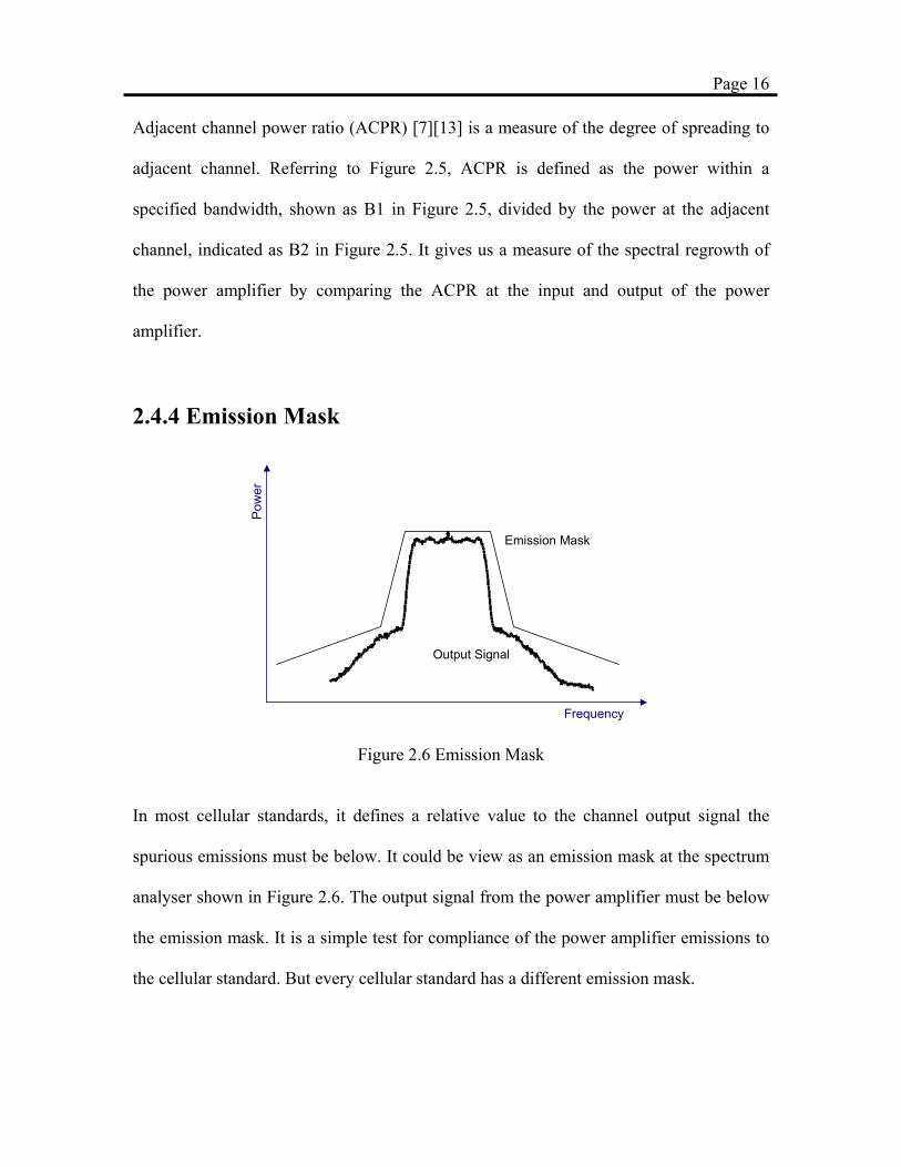
2.4.3 Adjacent Channel Power Rejection (ACPR)
Frequency
Amplitude
B1
B2
Figure 2.5 ACPR
Page 16
Adjacent channel power ratio (ACPR) [7][13] is a measure of the degree of spreading to
adjacent channel. Referring to Figure 2.5, ACPR is defined as the power within a
specified bandwidth, shown as B1 in Figure 2.5, divided by the power at the adjacent
channel, indicated as B2 in Figure 2.5. It gives us a measure of the spectral regrowth of
the power amplifier by comparing the ACPR at the input and output of the power
amplifier.
2.4.4 Emission Mask
Frequency
Pow
er
Emission Mask
Output Signal
Figure 2.6 Emission Mask
In most cellular standards, it defines a relative value to the channel output signal the
spurious emissions must be below. It could be view as an emission mask at the spectrum
analyser shown in Figure 2.6. The output signal from the power amplifier must be below
the emission mask. It is a simple test for compliance of the power amplifier emissions to
the cellular standard. But every cellular standard has a different emission mask.

Page 17
2.5 Linearization Linearization can be used to improve the linearity and efficiency of the power amplifier.
In this section, the five methods are discussed on the linearization of the power amplifier.
They are
a. Cartesian Feedback
b. Feedforward
c. Envelope Elimination and Restoration
d. Linear Amplification with Non-Linear Components
e. Predistortion
Each method has its limitations. It is implemented in different situation depending on a
various factors such as modulation bandwidth, complexity of the method, cost etc.
2.5.1 Cartesian Feedback Feedback has been traditionally used to linearize an audio frequency amplifier. It was
invented and patented by H. S. Black [14] in 1928. It has since used widely in low
frequency analog circuit to linearize a non-linear amplifier. The operational amplifier (op
amp) is an excellent example of feedback. The op amp itself has a very high gain but is
non-linear. But using feedback, it is able to create a linear amplifier but at a lower gain.
However, applying feedback directly to the RF power amplifier will not reduce the

Page 18
distortions significantly because normally RF power amplifier does not have enough gain
at high frequency. Also there is a problem of stability at RF frequency.
A modified version of the feedback is the Cartesian Feedback [7][15]. Figure 2.7 shows
the general block diagram.
0
90
0
90
PhaseShifter
-
-
+
+
Attenuator
Power AmplifierI
QCoupler
Figure 2.7 Cartesian Feedback
Part of the output of the power amplifier is sampled and demodulated back into I and Q
channel. It is feedback to the input to create an error signal. This error signal is filtered
out and modulated to the RF frequency and input to the power amplifier. The gain of the
power amplifier will definitely decrease due to the feedback. But it might decrease the
distortions of the power amplifier drastically.

Page 19
The main problem with Cartesian Feedback is the control of the phase shifter. The
feedback signal should not be in phase with the input otherwise it would lead to
instability. In order that the feedback signal to be out of phase with the input, the phase
shifter must be adjusted to meet this criteria. If the modulation bandwidth of the input
signal is wide, the phase changes from one part of the bandwidth to another. Therefore
the phase shifter must be able to automatically change its phase. The control of the phase
shifter is troublesome and not easily implemented. The other problem is that the feedback
path must be linear. The power amplifier would amplify any distortions in the feedback
path. Hence the Cartesian Feedback is currently used in narrowband systems.
2.5.2 Feedforward
Time Delay
Time Delay
Main PowerAmplifier
Error Amplifier
RFIN
RFOUT
PowerSplitter
Coupler
Figure 2.8 Feedforward Linearization
Figure 2.8 shows the general block diagram of the feedfoward linearization [16]. The RF
input is split into two branches. The main power amplifier will amplify the input signal

Page 20
with all the distortions of the power amplifier present. The other branch goes through a
time delay. A directional coupler will then couple part of the power into the second
branch. This will cancel out the linear portion of the signal, leaving the distortions to be
amplified by the error amplifier. At the output of the feedfoward system, the distortions
amplified by the error amplifier will cancel the distortions produce by the power
amplifier. Therefore at its output, it will have a linearized RF signal.
One of the problems in the feedfoward linearization is the time delay. The power
amplifier has to be characterize thoroughly so as to be able determine the time delays of
various components. It is unable to adapt to the changing environment if it not modified.
Some research work had been done in this area [17]. The other problem is that it requires
an error amplifier. This adds to the power consumption of the overall system. Also the
couplers and splitters used are passive, therefore lossy, components. This will also
decrease the efficiency of the overall system.
Feedforward linearization is an open loop linearization. Therefore it has much greater
bandwidth compared to feedback linearization. It is possible to obtain good linearity
performance. It is normally used in base stations.
Page 21
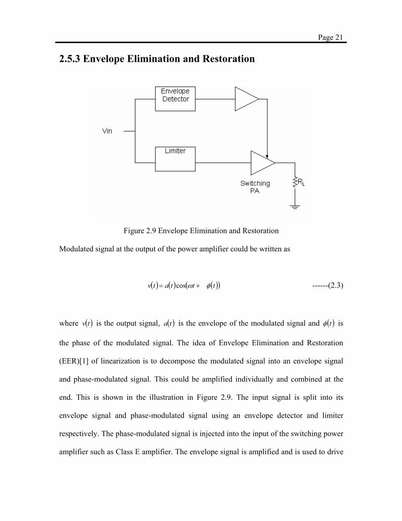
2.5.3 Envelope Elimination and Restoration
Figure 2.9 Envelope Elimination and Restoration Modulated signal at the output of the power amplifier could be written as
( ) ( ) ( )( )tttatv φω += cos ------(2.3)
where is the output signal, ( )tv ( )ta is the envelope of the modulated signal and ( )tφ is
the phase of the modulated signal. The idea of Envelope Elimination and Restoration
(EER)[1] of linearization is to decompose the modulated signal into an envelope signal
and phase-modulated signal. This could be amplified individually and combined at the
end. This is shown in the illustration in Figure 2.9. The input signal is split into its
envelope signal and phase-modulated signal using an envelope detector and limiter
respectively. The phase-modulated signal is injected into the input of the switching power
amplifier such as Class E amplifier. The envelope signal is amplified and is used to drive

Page 22
the supply line of the switching power amplifier. Therefore at the output of the switching
power amplifier, the modulated input signal is not only amplified but also its envelope
and phase is restored back. The advantage of this method is that we could use a non-
linear switching power amplifier thereby greatly improving the efficiency of the power
amplifier.
However, there are a few problems using this method. Firstly, to properly restore the
modulated signal at the output of the power amplifier, the phase shifts for the envelope
signal and the phase-modulated signal must be the same. This is difficult to accomplish
as the circuits used in the envelope signal and phase-modulated paths are very different.
Secondly, using a limiter to extract the phase-modulated signal introduce additional AM-
to-PM distortions.
2.5.4 Linear Amplification with Non-Linear Components
Figure 2.10 Linear Amplification with Non-Linear Components

Page 23
The idea for Linear Amplification with Non-Linear Components (LINC)[1][7]
linearization is to decompose the modulated signal given in Equation (2.3) into two
phase-modulated signals given in (2.4)
( ) ( )( )tttVv o θφω ++= sin5.01
( ) ( )( )tttVov θφω −+−= sin5.01 -----(2.4)
where and V is a constant. The block diagram for LINC is shown in
Figure 2.10. The input signal is split into two phase-modulated signals by the signal
separator. Then they will be amplified individually non-linear power amplifier such Class
E amplifier. Finally, the amplified signal is restore by combining the output signal of the
non-linear power amplifier together.
( ) ( )[ ]oVtat /sin 1−=θ o
The disadvantage of this method is that firstly it is difficult to implement the signal
separator in analog or RF domain. The circuits that had to be implemented are non-linear.
Secondly the phase delay of the two phase modulated signals must be the same. Thirdly,
the adder at the end must have high isolation between the two non-linear power
amplifiers else it will distort the final output signal.

Page 24
2.5.4 Predistortion
Input Output
Power AmplifierPredistorter
Figure 2.11 Basic principle of Predistortion
Figure 2.11 shows the basic principle of predistortion. A non-linear device, in this case a
power amplifier, could generate a linear output, if there is a predistorter that is inserted
before it. The characteristics of the predistorter must be the inverse of that from the
power amplifier. This technique is very general and is applicable in lot of applications.
The modeling of the non-linear device is crucial so that it is possible to generate a
predistorter that eliminate or reduce the distortions. As discussed in section 2.3, the
power amplifier could be modeled as an odd order power series. If it is restricted to a
third order power series, it could be written as in (2.5).
Vo = a1Vi + a3Vi3 ------(2.5)

Page 25
where Vo and Vi are the output and input of the power amplifier respectively. an are the
coefficients of the power amplifier. If the predistorter has a similar third order series as
shown in (2.6).
VP = β1V’i + β3V’i3 --------(2.6)
where VP and V’i are the output and input of the predistorter respectively. βn is the
coefficients of the predistorter. Since the predistorter is inserted before the power
amplifier, then Vi =VP. Therefore the output of the power amplifier is
Vo = a1β1 V’i + [a1β3 + a3β13] V’i
3 + 3 a1β12β3 V’i
5 + 3 a3β1β32V’i
7 + a3β33 V’i
9 (2.7)
From (2.7), it is possible to draw some possible implications using predistortion. Firstly,
it is possible to reduce the third order distortions by proper selection of the coefficients of
the predistorter. Theoretically, by choosing the correct coefficients, the third order
distortion could be eliminated. Secondly, as a third order predistorter, fifth, seventh and
ninth order distortion starts to appear. This is not present when the power amplifier is
used alone. It is possible to eliminate these higher order terms using a higher order
predistorter. But even higher order distortions terms will start to appear. In practice, these
higher order terms are generally much lower in amplitude compared to the third order
distortion. The combination of the predistorter and power amplifier will still improve the
linearity of the overall power amplifier. In an actual power amplifier, it does not behave

Page 26
exactly in manner described by a power series. Therefore the third order predistorter will
not eliminate all the third order distortion. One of things to take note is that it is quite
impossible to linearize the power amplifier if it is operating at the saturation point. The
power series model is impossible to describe power amplifier near or at the saturation
point.
The third order distortions generated by the power amplifier is the most serious. In order
to maximize the power efficiency of power amplifiers, it will be operating near to its
saturation point. Performing a two-tone test at the saturation point, the third order
distortions would have the highest distortion power levels compared to the rest of the
distortions. If the RF power amplifier is used in a multi-carrier system, the distortions
generated is even predominantly third order [18]. The fifth and higher order distortions
would also be present but these distortions have lower power levels.
The predistortion linearization is an open loop linearization method. Therefore it has a
wide bandwidth. Good linearity is able to obtain from this method. The most troublesome
problem is to find the correct coefficients for the power amplifier. Also the power
amplifier characteristics will drift in time, the predistorter should be able to track these
changes and modify the coefficients to maximize the linearity of the power amplifier.

Chapter 3
The Design of Analog Predistorter
Predistortion is simple and effective method of linearizing the power amplifier. Also
the power amplifier could be modelled as an odd order power series. Simply using
this odd order power series model, the predistorter is able reduce the distortion by
introducing a similar odd power series before the power amplifier.
In this chapter, the power amplifier’s model is slightly modified. Using the modified
model, an analog predistorter was designed and fabricated to linearize the power
amplifier. The major blocks of the design and different considerations of the blocks
are discussed. Finally the simulation, layout and die photo of the chip is presented.

Page 28
3.1 Introduction
The power amplifier model introduced in the previous chapter does not take into the
account the phase distortion. A more accurate model for the power amplifier is to use
complex coefficients so that they are complex values [19] as shown in (3.1).
Po = a1Pi + a3Pi3 + a5Pi
5 + ……..
= (a11 + j a11)P i + (a31 + j a31) Pi3 + (a51 + j a51) Pi
5 + …… (3.1)
In this modified model, the power series is still an odd order function. All the even
order distortions would be filtered out at the output of the power amplifier thus the
distortion it causes is not as significant as odd order distortions. The odd order power
series is able to model the intermodulation distortion (IMD). However, the model is
still a memoryless model.
Since the power amplifier could be more accurately modeled using complex
coefficients, the predistorter should also use complex coefficients to improve the
linearity of the power amplifier.
The third order intermodulation distortion (IMD3) is the most serious distortion
generated by the power amplifier. If the predistorter is able to reduce the IMD3 of the
power amplifier, the linearity of the power amplifier would be greatly improved. This
is especially true in multi-carrier systems[18] where the distortions is caused
predominantly by IMD3. For example, in [20] 3 carriers were injected to a power
amplifier. The measured IMD3 was at least 31dB greater than the IMD5. In practical

Page 29
power amplifier, the coefficients 35 aa << . If the injected signal has n carriers, the
IMD3 products generated, such as wi+wi+1-wi-2 and 2wi-wi+1 where wi is frequency of
the ith carrier, will be more significant than IMD5.
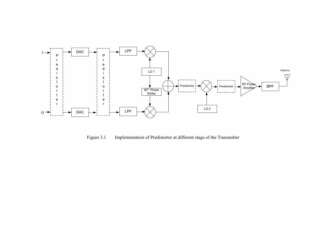
The predistorter could be implemented at several different stages of the transmitter
chain. Figure 3.1 shows the different sections in the transmitter where the predistorter
could be implemented. The predistorter could be implemented at the baseband before
the digital-to-analog converter (DAC) [21]. Most likely the predistorter will be one of
the modules at the baseband implemented by a digital signal processor (DSP). The
advantage of this approach is its flexiblility. To change any part of the predistorter, it
is merely changing the software written into the DSP. Also it is quite simple to
implement the adaptive algorithm to find the optimum coefficients for the
predistorter. But by using this approach, a high processing power DSP must be
acquired which will increase the power consumption of the transmitter.
The predistorter could also be used after the DAC. Therefore it is still at baseband but
now the predistorter is implemented using analog circuits [19][22]. The power
consumption in this approach is lower than the digital predistortion. One of the
problems to take note is the distortion caused by the analog circuit in the predistorter.
Any unwanted distortion caused by the predistorter does not help to reduce the
distortion in the power amplifier. Instead, it will be amplified by the power amplifier
nullifying the linearizing effect of the predistorter. This is true for all analog, IF and
RF predistorter.

Page 30
The predistorter implemented at IF is similar to the one implemented at the analog
baseband but the bandwidth of the predistorter increased. It is easier to filter out the
unwanted even order harmonics of predistorter than at baseband. It is impossible to
filter these distortions at baseband because these even order harmonic distortion falls
right in your bandwidth. However, predistorter implemented in IF stage requires a
ninety degree phase shifter. If implemented in integrated circuit, the phase shifter may
occupy a substantial die area.
If the predistorter is implemented at RF, the high frequency characteristics of the
integrated chip is very diffcult to control. Hence RF predistorter [11] has very limited
flexibility compared to the rest of the predistorters. Normally, it consists of diodes and
some passive components. It has to be designed individually for each type of power
amplifier and is difficult to tune when the power amplifier drifts.
I
Q
Antenna
RF PowerAmplifier
LO 1
900 PhaseShifter
DAC
DAC
Predistorter
Predistorter
Predistorter
LO 2
Predistorter
LPF
LPF
BPF
Figure 3.1 Implementation of Predistorter at different stage of the Transmitter

Page 32
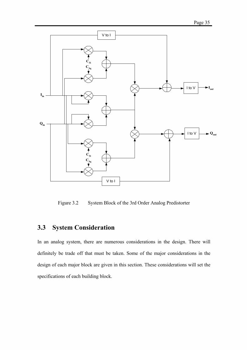
3.2 System block of the analog predistorter
From the discussions in the previous section, there are various options where the
predistorter could be implemented in the transmitter chain. A complex analog
predistorter operating in the baseband to low IF stage was implemented. The current
consumption operating in the analog domain is lower compared to digital techniques.
Designing the predistorter to operate from baseband to IF frequency gives it a greater
flexibility. A third order complex analog predistorter was designed to cancel out third
order intermodulation distortion (IMD3), which is the major source of distortion in the
power amplifier. IMD3 is even more dominant in multi-carrier systems. The
bandwidth of the predistorter chip is 20Mhz. The phase shifter which is required for
the operation in IF predistortion is implemented using an external discrete device. A
SiGe BiCMOS process was used because it was the available process at that time.
Also it was because most high performance radio frequency chips are fabricated using
BiCMOS process rather than pure CMOS process.
In linear modulation, the transmitter has I and Q channels as shown in Figure 3.1. I
and Q channels will be upconverted with a carrier frequency that is ninety degrees out
of phase with each other. These two channels could be used as the complex input to
the predistorter. Therefore the odd order power series used by the predistorter to
linearize the power amplifier could be modified to one shown in (3.2) [19].
( ) ( )( )2331 rjccjQIjQI qiininoo +++=+
= [Iin + (c3iIin + c3qQin) |r|2 ] + j[Qin + (c3qIin + c3iQin) |r|2] (3.2)

Page 33
Given that 22inin QIr +=
Iin and Qin are input signal of I and Q channel respectively. Io and Qo are the output
signals of I and Q channel respectively of the analog predistorter. c3i and c3q are the
variable coefficients of the predistorter to compensate different power amplifiers
characteristics . |r|2 is basically the squares of the envelopes and is related to the
power of the signal.
The block diagram of the analog predistorter is given in Figure 3.2. The major blocks
of the predistorter chip are the analog multipliers, transconductor and transimpedance
cells. The most important block of the chip is the analog multiplier. From the equation
(3.2), there are many of multiplication operation between c3i, c3q and |r|2. A total of
eight multipliers are required in this chip and it occupies the most die area in the
design. The output swing after each multiplication tends to get smaller. To have
enough signal swing for the next stage of multiplication, amplifiers are required. To
minimise the number of amplifiers, the system design that was adopted minimise the
number of stages of multiplication. Therefore out of the eight multipliers in the chip,
six multipliers are placed at the first stage of operation.
The addition operation shown in the Figure 3.2 could easily be implemented if it is in
current mode by tying the output currents of two different blocks together. It also
requires the transimpedance to convert the current output to voltage, driving the
external load. If implemented in discrete form such as on a PCB, addition operation is
done using operational amplifiers. These greatly increase the power consumption and
noise of the design.

Page 34
Not shown in the block diagram are the level shifters, amplifiers and buffers. These
blocks are critical to the proper operation of the chip. They are mainly use to
condition the signal so that it could be use for the next stage. The level shifters are
used because the operating frequency includes d.c. Therefore it cannot use a.c
coupling. The level shifters change the d.c at output of the blocks to the appropriate
level needed for the next stage. This requires careful planning for the different parts of
the chip. The amplifiers are used to amplify the output signal to acceptable level for
processing for the next stage. The most power consuming part of the chip is the
buffer. It is used to drive the external load of the chip.
Page 35
Iin
Qin
C3i
C3q
C3i
C3q
V to I
V to I
Iout
Qout
I to V
I to V
Figure 3.2 System Block of the 3rd Order Analog Predistorter
3.3 System Consideration
In an analog system, there are numerous considerations in the design. There will
definitely be trade off that must be taken. Some of the major considerations in the
design of each major block are given in this section. These considerations will set the
specifications of each building block.

Page 36
a. Output Signal Swing
As seen in the Figure 3.2, there are quite a number of stages in the design. The output
signal swing of each building block must be sufficient to drive the next stage.
Therefore, the gain of each individual block must be calculated. The lower the output
voltage swing, the lower is the signal-to-noise ratio (SNR). This will increase the
noise of the system. Therefore the output signal of each individual block must be high
enough to be detected. The last stage of the chip is a transimpedance cell. It is going
to drive the pads of the chip, which will consume the most current. The output swing
of this cell must be defined for the whole range of coefficients for the predistorter else
it will waste current.
b. Distortions
As the predistorter is going to change the waveform of the original signal, it is critical
that the predistorter’s own distortion be as low as possible. If the predistorter
introduces additional unwanted distortions, it will be amplify by the variable gain
amplifiers and power amplifier. This will cause the power amplifier be more non-
linear. As there are eight analog multipliers, they are the most crucial cells in the
design. Careful design must be taken to reduce the distortion caused by the analog
multipliers. It might have to trade off power consumption with distortion.

Page 37
c. Bandwidth
The bandwidth of the chip is designed to be from d.c to 20Mhz to cater for the high
data rate at baseband and IF. The internal blocks of the chip will have a bandwidth
that is higher than 20Mhz. This is because the individual blocks needs to drive the
internal nodes in the system.
The process that was used in the design was a 0.8 µm SiGe BiCMOS. Generally in
analog design the lowest feature size of the MOS is avoided to minimise mismatch.
Using a higher feature size will have a better matching between transistors and higher
output impedance. But higher size has a lower cutoff frequency. Therefore some
tradeoffs or design techniques have to be implemented to meet the bandwidth
specification. Normally the trade off for a higher bandwidth is the power
consumption.
d. Noise
Noise generated by the predistorter should be kept to the minimum. This is especially
for the analog multipliers as they generate the most noise. Normal linear analysis of
noise could not be directly applied to the analog multipliers. A modified analysis has
to be done on the multipliers. The biasing point determines the noise generated by the
different blocks.

Page 38
e. Power consumption
The power consumption of the predistorter should be as low as possible. If it is to be
used in mobile terminals, the power consumption of the predistorter is even stricter. It
will not justify the addition of the predistorter in the transmitter chain if the reduction
of the distortion could be achieved by backing off the power amplifier.
From the above discussions, there are quite a number of compromises or trade offs to
be made in the design of the predistorter. Therefore each individual block requires
careful planning of its specifications.

Page 39
3.4 Circuit Implementation
In this section, the major building blocks for the predistorter will be discussed in
detail. Each of these circuits has to be designed with proper consideration of the
different trade offs.
3.4.1 Analog Multiplier
3.4.1.1 Brief Survey From Figure 3.2, analog multiplier is the most important building block of the
predistorter. The function of the analog multiplier is to perform a linear product of
two variables.
Z = Kxy (3.3)
K is a multiplication coefficient with suitable dimension. The variables x, y and z
could be in voltages or currents. Analog multipliers are widely used as signal
processing elements such as amplitude modulators, mixers etc. As multiplication
operation is not a linear operation, small signal analysis used in linear analog circuit
design could not be used. Also a simple implementation of feedback theory is
incorrect.
Analog multipliers could be implemented using bipolar transistors or CMOS. The
bipolar transistor implementation uses the translinear [23] property of the transistor
which was first introduced by Barrie Gilbert [24]. A basic four quadrant analog
multiplier is shown in Figure 3.3.

Page 40
DC
TransconductorTransconductorVx+
Vx-
Vy-
Vy-
Iy- Iy+ Ix- Ix-
Io- Io+
Figure 3.3 A Basic Bipolar implementation of Analog Mulitplier
The multiplier operate in the current domain, the output of the multiplier is
yxo III ×= (3.4)
Because the multiplier operates in the current domain, it requires transconductor cells
to convert both the differential input voltages Vx+, Vx- and Vy+, Vy- into current. The
output of the multiplier also needs resistors to convert the current back to voltage. The
bandwidth of the core bipolar multiplier is very wide. The critical issue is in the
design of the transconductor. The transconductor has to very linear and a wide
bandwidth to match the bandwidth of the multiplier.
As digital technology dominated modern electronics, sometimes it is required to
design analog circuits in CMOS. There are two general methods to make a four
quadrant multiplier in CMOS and are shown in Figure 3.4 where x and y are the
inputs to the multiplier. In Figure 3.4a, the multiplier consists of four single-quadrant
multiplier. In Figure 3.4b, the multiplier makes use of the four square law devices.
Both the single-quadrant multiplier and square law device could be implemented in
CMOS by operating the MOS either in linear or saturation region.

Page 41
x
-x
-y
y
y
xy
-xy
xy
-xy
+
-
4xy
(a)
Square LawDevice
Square LawDevice
Square LawDevice
Square LawDevice
x+y
-x+y
-x-y
x-y
X2+2xy+y2
X2-2xy+y2
X2+2xy+y2
X2-2xy+y2
+
-
8XY
(b)
Figure 3.4 Two general method of implementing analog multiplier in CMOS
A first order MOS model could express the output current of the MOS as
( )[ ]25.0 dsdstgsd VVVVKI −−= (Linear region of operation)
[ ]2tgsd VVKI −= (Saturation region of operation) (3.5) where ( LWCK ox / )µ= . All symbols have the conventional notation for MOS. From
the equation (3.5), it shows that there is more than one method of implementing the

Page 42
analog multiplier using MOS device. For example, the V term in the linear region of
operation for the MOS could be used as the square law device to implement the
multiplier shown in Figure 3.4b. But the linearity of this type of multiplier will be
poor. There are altogether seven ways [25] to build a four-quadrant multiplier using
MOS operating in linear or saturation region. Out of the seven ways, there are only
two methods that are most feasible and require lesser number of external circuits.
2ds
tV −
)2
The first method is to inject the one of the inputs of the multiplier at the gate of the
MOS and the other input at the source. The MOS transistor is operating in saturation
mode. If V and V are the input voltage signals, x y
[ ]2tyxd VVVKI −+=
( ) ( )[ ]22 2 tyxyx VVVVVK +−+= (3.6)
This transistor forms one part of the multiplier. By injecting the appropriate signal,
, , and , as shown in Figure 3.4b a fully functional four-quadrant
multiplier could be made.
xV yV xV− yV−
The second method is to use the MOS transistor in the linear region of operation. One
of the input signals, V , is injected at the gate and the other input, V , is injected at
the drain. The output signal is
x y
( 5.0 ytyyxd VVVVVKI −−= (3.7)

Page 43
The output signal contains the product of V and V and other unwanted terms, V
and . This output signal will form one of the single-quadrant multiplier shown
in Figure 3.4a. By injecting the appropriate input signals, V , , and − , to
the four single- quadrant multipliers, a full four-quadrant multiplier could be formed.
The other unwanted signals in equation (3.7) will be cancelled out at the output of the
full four-quadrant multiplier.
x y tyV
y
25.0 yV
x yV xV− V
A comparison of two methods in designing the four-quadrant multiplier is done in
[25]. It compares linearity, noise, matching etc. It concludes that in most performance
parameters the second method of implementation of analog multiplier is better than
the first.
In this brief survey excluded is the implementation of MOS analog multiplier in
subthreshold mode of operation. When the MOS is working in the subthreshold mode,
the MOS has characteristics similar to the bipolar transistor. However, the output
currents in this mode of operation are low making the circuit noisy.
3.4.1.2 Implementation of Analog Multiplier
From the discussion in the previous section, by injecting the input signals at gate and
drain of a MOS, it is possible to design a full four-quadrant analog multiplier. The
circuit topology is shown in Figure 3.5.

Page 44
Iout+ Iout-
Vy+ Vy-
Vx+Vx-Vx+
Figure 3.5 Analog Multiplier
All the nMOS transistors are operating in the linear region. The bipolar transistors,
offered in the BiCMOS process, offer a convenient way to bias the V of the MOS
transistors and inject V signal to the drain the nMOS. The V of the nMOS transistor
could be made to track the input signal V by using gain boosting techniques [26].
The output current of the analog multiplier is
ds
y ds
x
( )( )−+−+−+ −−=− yyxxnoutout VVVVLWCoxii )/(µ (3.8)
where nµ , and ( are all the MOS circuit device parameters. This analog
multiplier has a better linear response than the folded Gilbert cell multiplier used in
[19].
oxC )LW /
From the block diagram, shown in Figure 3.2, there are many multiplications that are
done in parallel. As the output of the analog multiplier is current, it is quite simple to
add the output current of another multiplier by tying their outputs together thereby
reducing the number of MOS transistors.

Page 45
To drive the next stage of multiplications, the output currents of the analog multiplier
have to be converted to voltage. Adding resistors as load is simplest way for doing
that. However resistors occupy a large amount of die area compared to MOS. Using a
diode connected MOS, it is possible to replace the resistors. However, the distortions
caused by the MOS resistors must be kept to a minimum.
Although the diode connected MOS could replace the resistors, its low resistance
cause the output voltage swing to be low too. In order to increase the resistance,
conventionally, the aspect ratio of the MOS has to be decreased. But that degrades the
matching of the diode connected MOS. To increase the resistance, positive feedback
[27] was used. The positive feedback transistor used must have a smaller dimension
than the diode connected transistor else oscillations would occur. The non-linearity
caused by the MOS resistors with the positive feedback must be simulated.
To calculate the sizes for the nMOS used in the analog multiplier, as shown in Figure
3.5, the input voltage swing and the output current had to be determined. If
, ( ) 8.0=− −+ xx VV ( ) 4.0=− −+ yy VV and the output current is determined to be
Aii outout µ100=− −+ , using the Equation (3.8), the obtained 3≈L
W given that
. Therefore the initial size used in the simulation was 2/100 ACoxn µµ =
mW
V
µ6= Land mµ2= . The minimum size of mL µ8.0= is avoided so as to obtain
better matching between the four nMOS transistor. If the output voltage of the analog
multiplier is 500mV for i Aioutout µ100=−+ − then the transconductance of the diode
connected pMOS with the positive feedback pMOS is Sµ200 .

Page 46
The transconductance of a MOS is given in (3.9).
dm IL
WCoxg
= µ2 (3.9)
Given nµ , are all the MOS circuit device parameters,oxC
LW is the MOS device
size and is the drain current of the MOS. dI
The current drawn by one branch of nMOS could be calculated from Equation (3.10).
( )[ ]25.0 dsdstgsnd VVVVLWCoxI −−= µ (3.10)
If , 2/100 VACoxn µµ = 3=L
W , 8.0=tV V and V and is bias to 1.6V and 0.4V
respectively then current through the nMOS is
gs dsV
Aµ72 . The biasing of V and is
choosen so that the nMOS operates in the linear region.
gs dsV
Referring to Figure 3.6, the total drain current through each pair of the diode
connected pMOS and positive feedback pMOS is AAx µµ 288724 = .If the size of the
feedback pMOS is set to half the diode connected pMOS, then the transconductance
and current of the positive feedback transistor is half of the diode connected transistor
but it will reduce the total transconductance of diode connected transistor by two
times. Therefore the transconductance and drain current of the diode connected pMOS
is set Sµ400 and respectively and using Equation (3.9) the device ratio of the
diode connected pMOS is 11.90 given that . Therefore a reasonable
size of the diode connected pMOS was set to W
uA192
2/35 VAµ=
m
Coxpµ
µ24= and mL µ2= .
Page 47
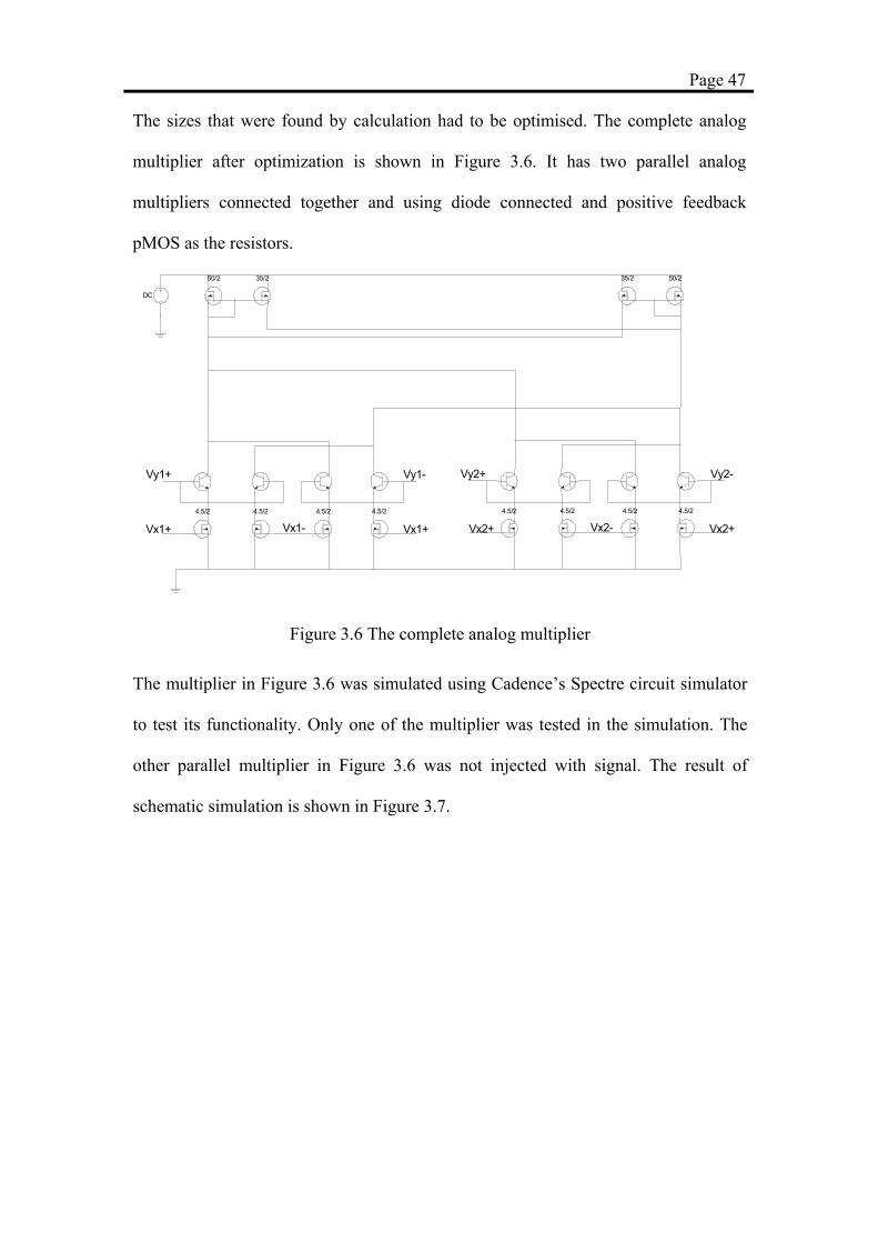
The sizes that were found by calculation had to be optimised. The complete analog
multiplier after optimization is shown in Figure 3.6. It has two parallel analog
multipliers connected together and using diode connected and positive feedback
pMOS as the resistors.
4.5/2 4.5/24.5/2 4.5/2
Vy1+ Vy1-
Vx1+Vx1-Vx1+
4.5/2 4.5/24.5/2 4.5/2
Vy2+ Vy2-
Vx2+Vx2-Vx2+
50/2 35/2 50/235/2
DC
Figure 3.6 The complete analog multiplier
The multiplier in Figure 3.6 was simulated using Cadence’s Spectre circuit simulator
to test its functionality. Only one of the multiplier was tested in the simulation. The
other parallel multiplier in Figure 3.6 was not injected with signal. The result of
schematic simulation is shown in Figure 3.7.
Page 48
Vy=400mV
Vy=300mV
Vy=200mV
Vy=100mV
Vy= -100mV
Vy= -200mV
Vy= -300mV
Vy= -400mV
Vx (V)
Vout
(V)
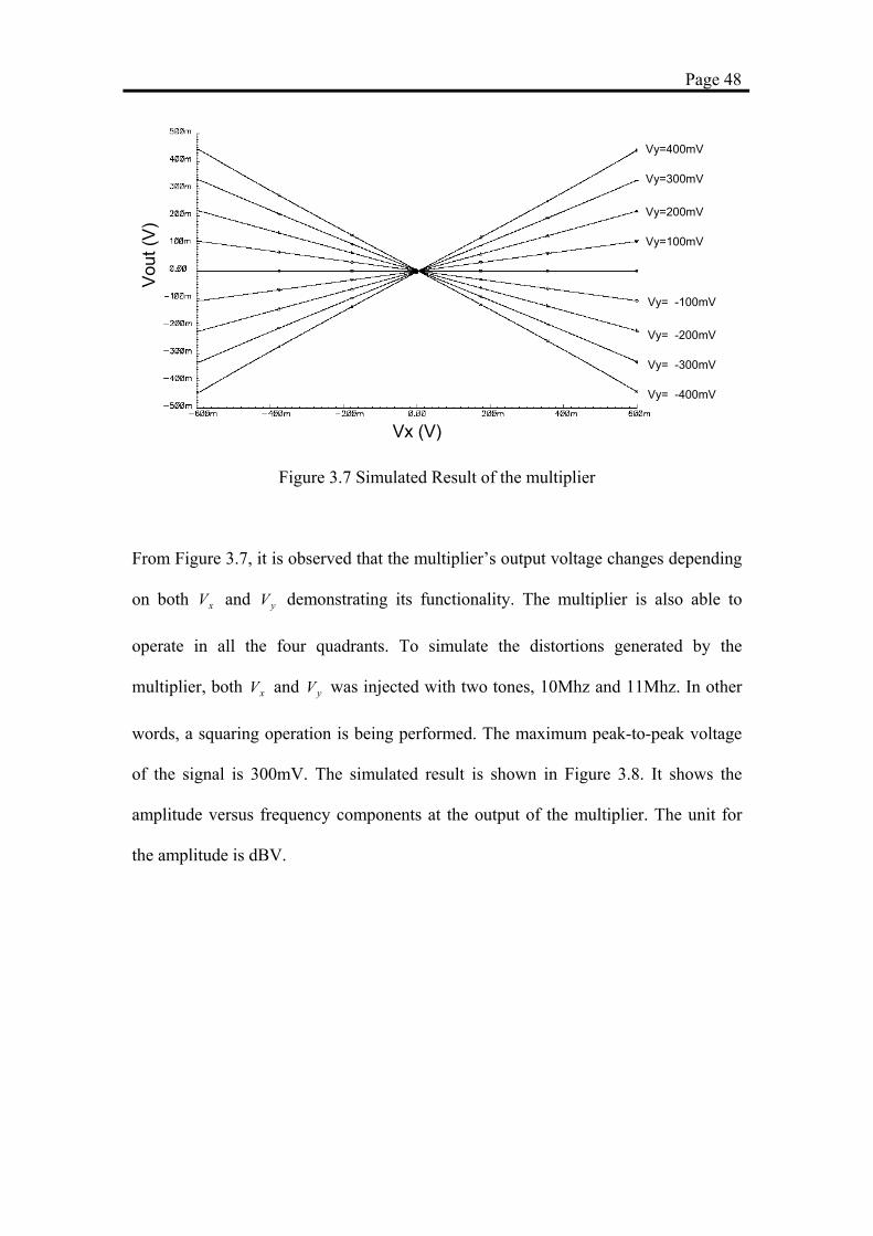
Figure 3.7 Simulated Result of the multiplier
From Figure 3.7, it is observed that the multiplier’s output voltage changes depending
on both V and V demonstrating its functionality. The multiplier is also able to
operate in all the four quadrants. To simulate the distortions generated by the
multiplier, both V and V was injected with two tones, 10Mhz and 11Mhz. In other
words, a squaring operation is being performed. The maximum peak-to-peak voltage
of the signal is 300mV. The simulated result is shown in Figure 3.8. It shows the
amplitude versus frequency components at the output of the multiplier. The unit for
the amplitude is dBV.
x y
x y
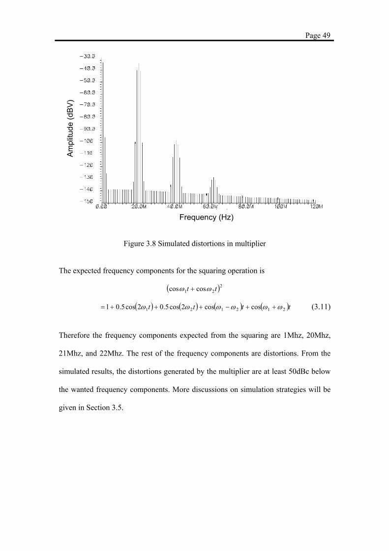
Page 49
Frequency (Hz)
Ampl
itude
(dBV
)
Figure 3.8 Simulated distortions in multiplier
The expected frequency components for the squaring operation is
( )221 coscos tt ωω +
( ) ( ) ( ) ( )tttt 212121 coscos2cos5.02cos5.01 ωωωωωω ++−+++= (3.11)
Therefore the frequency components expected from the squaring are 1Mhz, 20Mhz,
21Mhz, and 22Mhz. The rest of the frequency components are distortions. From the
simulated results, the distortions generated by the multiplier are at least 50dBc below
the wanted frequency components. More discussions on simulation strategies will be
given in Section 3.5.
Page 50
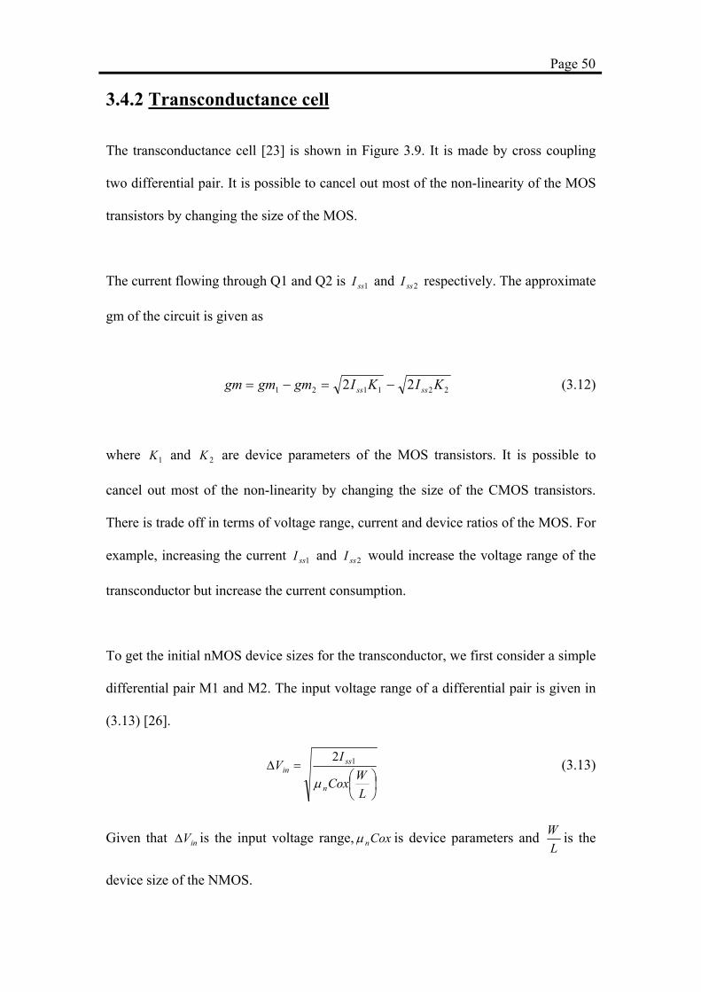
3.4.2 Transconductance cell The transconductance cell [23] is shown in Figure 3.9. It is made by cross coupling
two differential pair. It is possible to cancel out most of the non-linearity of the MOS
transistors by changing the size of the MOS.
The current flowing through Q1 and Q2 is and respectively. The approximate
gm of the circuit is given as
1ssI 2ssI
221121 22 KIKIgmgmgm ssss −=−= (3.12)
where and are device parameters of the MOS transistors. It is possible to
cancel out most of the non-linearity by changing the size of the CMOS transistors.
There is trade off in terms of voltage range, current and device ratios of the MOS. For
example, increasing the current and would increase the voltage range of the
transconductor but increase the current consumption.
1K 2K
1ssI 2ssI
To get the initial nMOS device sizes for the transconductor, we first consider a simple
differential pair M1 and M2. The input voltage range of a differential pair is given in
(3.13) [26].
=∆
LWCox
IV
n
ssin
µ
12 (3.13)
Given that is the input voltage range,inV∆ Coxnµ is device parameters and L
W is the
device size of the NMOS.

Page 51
If , , which is obtained from the foundry’s datasheet,
and setting
VVin 8.0=∆
I
2/100 VACoxn µµ =
Ass µ1201 = , the device ratio obtained is 1ML
W is 3.75. The device ratio
recommended in [23] for M3 and M4 is
=
3126.1
MM LW
LW if the current is set to
be two times of . Running through circuit simulations, the final optimum device
sizes of the NMOS for this process is given in Figure 3.9.
2ssI
1ssI
M110/2
M37/2
M47/2
M210/2
Q1
Q2
Vin+ Vin-
Va
Vb
Figure 3.9 Transconductance cell The simulated output current versus input voltage is given in Figure 3.10.

Page 52
Input Voltage (V)
Out
put
Cur
rent
(A)
Figure 3.10 Simulated results of the transconductance cell
From the simulation, the transconductance cell is able to convert input voltage to
output current from –800mV to 800mV. The output current will taper off for any
voltage greater than –800mV or 800mV.
3.4.3 Transimpedance cell and Output Buffer
In order to drive the pads of the chip, it is required to convert the final output currents
of the predistorter into a voltage. MOS transistors is used as resistors, similar to the
load in the design of the analog multiplier, to converts the output current to voltage.
The schematic diagram is Figure 3.11.

Page 53
65/2 65/2
8/2 8/2
DC
Vref
Iin+ Iin-
Figure 3.11 Transimpedance cell
+inI and are the final output currents of the predistorter. It is injected into the
diode connected MOS transistor. V is used to set the biasing current for the diode
connected MOS. Since the output is differential, the matching of both nMOS is quite
critical.
−inI
ref
The buffer is the last stage of the predistorter and is used to drive the output voltage
out of the chip. It has to drive the chip’s pads, bond wires of the package and external
parasitic capacitances of the copper conductor. Therefore the current consumption of
the buffer is the highest for the whole predistorter. The schematic diagram is shown in
Figure 3.12. It is made up of two stages of emitter follower. The first stage emitter
follower used the pMOS as the active device. This is because MOS devices do not
require a base current. Bipolar device is used as the active device in the second stage
of the buffer. It has better current handling capabilities than the MOS. The emitter

Page 54
followers are basically class A amplifiers. Therefore the efficiency of the buffer is
very low. However, the buffers will give the most linear response.
20/2
100/2
Vin
Vref
DC
DC Iref
Figure 3.12 Output Buffer
3.5 Simulation
The circuit that was discussed in the previous section has to be simulated to check
whether they conform to the specifications. Cadence’s Spectre RF [28] was used as
the simulator. The simulator provides an integrated environment for schematic capture
and simulation. It includes quite a wide range of different types of simulation such as
d.c analysis, transient, s parameters etc.
The first thing to note during the design was that it was quite impossible to simulate
the whole transimitter chain with the predistorter added. The simulation will require
too many resources in terms of memory and hard disk space. This is because the
amount of processing required for both baseband and RF frequency is too high. The

Page 55
simulation time will be very long. Even if there are sufficient resources, the
simulation might not converge.
Some of simulation strategies taken in the design are
a. Each individual block was simulated first before they are connected together.
If the individual bock does not work then it is impossible for the different
connected blocks to work properly.
b. The first type of simulation to be done is the d.c analysis. If the biasing of the
block is incorrect then it is useless to run the rest of different types of
simulation.
c. The analog multiplier is not a linear device therefore a small signal a.c.
analysis will not be a sufficient to determine the bandwidth. A transient
analysis was done at several different frequencies to ascertain the bandwidth.
d. Two frequency tones are injected into the predistorter and the output is
observed in both the frequency and time domain. Simulating modern
modulation techniques such as QAM, QPSK will increase the simulation time
drastically. The coefficients of the predistorter have to vary from the
maximum to the minimum to determine the functionality of the different
blocks.

Page 56
e. Integrated circuit design has to take into account of the changes in MOS and
BJT parameters due to process variations. These variations are inevitable in an
integrated circuit design. The worse case scenarios for process variations are
measured by the wafer fabrication manufacturers and are included in the
process files. It is required to run the design through the different changes in
the process and check that it meets the specifications. Unlike circuit design
with discrete components, it is impossible to change the circuit when the chip
is fabricated.
3.6 Layout
The layout of the chip is critical to the design flow. Any uncorrected errors in the
layout will affect the performance of the circuit directly. In analog integrated circuit
design, the functionally of the circuit is more important than the die space it occupies.
Also the number of the transistors in analog circuit is much lower than digital. Some
of the precautions and rules [29] use in the layout are
a. Matching
There are many differential pairs in the design. To match the characteristics of the
differential pairs to be almost the same as each other, they are placed side by side of
each other. Then the process variations that happen in the chip will normally affect the
differential pairs in equal portion.

Page 57
b. Wire Length
It is important to work out which are the critical nets. This will ensure that priority be
given in the routing of these critical nets. Generally these critical nets have the
shortest distance to the different active devices. The shortest length will ensure the
lowest voltage drop across the resistance in the metal that is used to conduct the
different active devices together.
c. Floor Planning
Before any thing is drawn of the chip, a floor plan must be ready. The floor plan gives
us a general idea where the different blocks of the circuit will be in the chip. A floor
plan had to be chosen that reduces the lengths of the metal. It allows us to estimate the
size of the chip. Also the floor plan tells us how the pins are to be arranged. With all
these information, the appropriate package for the design is chosen.
d. Noise
A noisy circuit will greatly affect the performance of the circuit especially a analog
circuit. One of the sources of noise is through the substrate. In order to reduce the
effects of noise, guard rings are placed in all the major blocks. These guard rings will
isolate the different blocks with each other. Decoupling capacitor is placed in most of
the major blocks to reduce the effects of power supply variations.
e. Parasitics
There are parasitic capacitances in all the circuit elements i.e. there is a parasitic
capacitor between two metal wires. It is especially important in analog design to take
into account the parasitic capacitances. These parasitic capacitances must not affect

Page 58
performance of chip. In order to know the parasitic capacitances, the layout has to be
drawn. There is software that will extract different parasitic capacitances. The
extracted capacitances will be re-simulated to check for its performances. If the
performance fails specification, you could either change the layout to a more optimize
one or change the circuit element.

Page 59
3.7 Completed Chip
The fabricated chip is shown in Figure 3.13. The die is 2.8 mm x 2.8 mm and the
package used is CLCC28. Included in the chip is a bandgap. It is to provide bias
current for the rest of the chip. The total current consumption is 30mA. However, the
current consumption of the core predistorter is only 10mA. This excludes the power
consume by the bandgap and output buffers. The supply voltage used in the design
3.3v. The netlist of the whole chip is included in the Appendix for referral.
Figure 3.13 Die photo of the predistorter

Chapter 4
Tests Results for the Analog
Predistorter
In this chapter, the results of the predistorter chip are presented. The analog
predistorter was designed to operate at baseband and low-IF frequency. The test
results for the low-IF were first presented in the low-IF. Two-tone test was first
performed on the predistorter. This is a simple and basic test for the linearization to
the power amplifier. Then different types of signals such as multi-carrier, OFDM
(Orthogonal Frequency Division Modulation) and CDMA (Code Division Multiple
Access) are injected into the predistorter so as to linearize the power amplifier. The
different types of signals require different metric of measurement such as ACPR
(Adjacent Channel Power Rejection) and NPR (Noise Power Ratio). In the next
section, the test results for the baseband were shown. Similar tests used in the low-IF
were done in the baseband. Finally, the predistorter extends its usage into the ROF
(Radio Over Fiber) system. This extension to ROF presents a novel use of the
predistorter and some results were presented.

Page 61
4.1 Predistorter Performance
The predistorter was tested for its own performance. A summary of results of the
predistorter is shown in Table 4.1. A two-tone test was performed on the analog
predistorter. The coefficients of the predistorter were adjusted by changing the input
voltage to the analog predistorter using a potentiometer. The third order products that
were generated by the analog predistorter would be used to linearize the non-
linearities in the power amplifier. From the two-tone test, it was observed that second
order distortions were also generated by the analog predistorter. These unwanted
distortions will degrade the performance of the predistorter. More discussions on
these distortions will be presented in Section 4.3
Simulated Performance Actual Performance
Supply Voltage 3.3v 3.3v
Total Current Consumption
30mA 32mA
Bandwidth 20Mhz 20Mhz
Input Voltage Range of Coefficients(c3i, c3q)
-400mV to 400mV -400mV to 400mV
Maximum Third Order Products the analog predistorter that could be generated
11dBc compared to the fundamental two-tone signal
12dBc compared to the fundamental two-tone signal
Distortions All distortions are >33dbc compared to the fundamental two-tone signal
Second order distortions is generated and is 21dBc below the fundamental two-tones signal
Table 4.1 Performance of Predistorter

Page 62
4.2 Low-IF Analog predistortion
4.2.1 Two-Tone Tests
The RF power amplifier used is RF2161 manufactured by RF Micro Devices [4]. It
was firstly characterised before the predistorter was added. A power detector was
used to measure the Pout verses Pin plot of the power amplifier and is shown in
Figure 4.1. The power amplifier has a linear gain of about 27dB till it saturates at
about 27dBm. A higher input power will not drive the power amplifier to deliver
power greater than its saturation point.
15
17
19
21
23
25
27
29
-15 -10 -5 0 5 10
Pin(dbm)
Pout
(dbm
)
Figure 4.1 Pout vs Pin of the power amplifier
A 2-tone test was performed on the power amplifier alone. The power levels of the
fundamental, third order intermodulation distortion (IMD3) and the fifth order
intermodulation (IMD5) were shown in Figure 4.2. The output of the power amplifier

Page 63
was attenuated by 20dB before it was measured by the spectrum analyser. It shows a
typical graph of a power amplifier. The gradient of the IMD5 is the highest followed
by IMD3 and then the fundamental power. The greatest distortion is caused by IMD3
because the power level is the highest.
-80
-70
-60
-50
-40
-30
-20
-10
0
10
-25 -23 -21 -19 -17 -15 -13 -11 -9 -7 -5 -3
Pin(dbm)
Pout
(dbm
) Pout(dbm) FundatmentalPout(dbm) IMD3Pout(dbm) IMD5
Figure 4.2 A Two Tone Test performed on the power amplifier
The predistortion chip was tested at low-IF frequency. The input signal is upconverted
to IF frequency at 20Mhz. The predistorter accepts the in phase and quadrature phase
of the input signal. It then predistorts the signal and is upconverted again to RF
frequency. Finally it is injected to the RF power amplifier. The test setup is shown in
Figure 4.3.
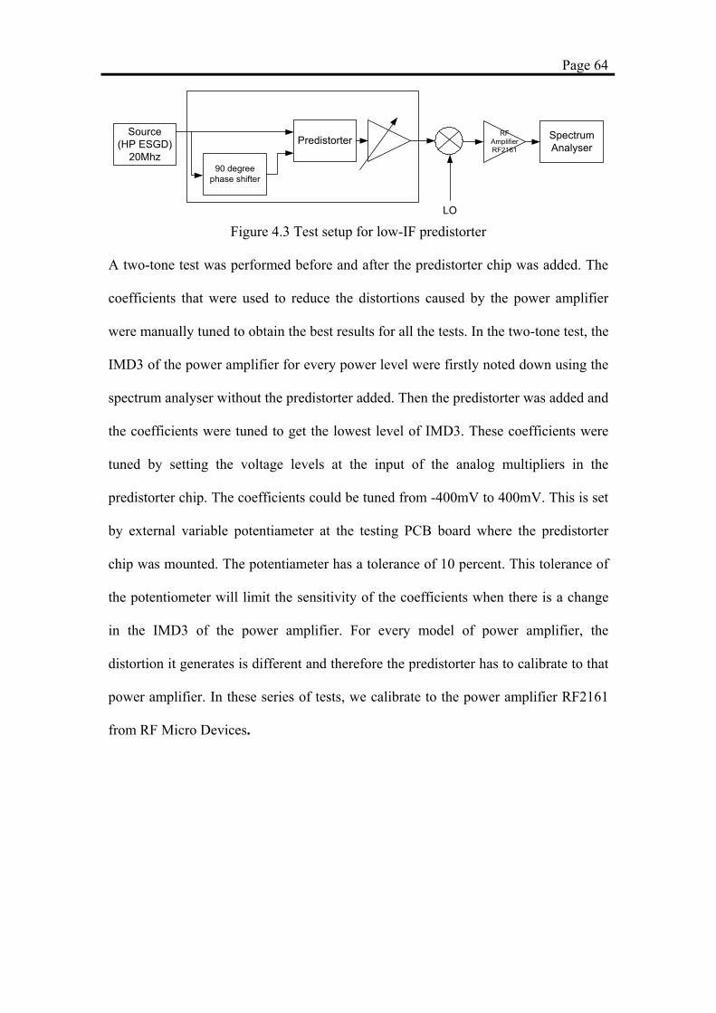
Page 64
Source(HP ESGD)
20MhzPredistorter
RFAmplifierRF2161
SpectrumAnalyser
LO
90 degreephase shifter
Figure 4.3 Test setup for low-IF predistorter
A two-tone test was performed before and after the predistorter chip was added. The
coefficients that were used to reduce the distortions caused by the power amplifier
were manually tuned to obtain the best results for all the tests. In the two-tone test, the
IMD3 of the power amplifier for every power level were firstly noted down using the
spectrum analyser without the predistorter added. Then the predistorter was added and
the coefficients were tuned to get the lowest level of IMD3. These coefficients were
tuned by setting the voltage levels at the input of the analog multipliers in the
predistorter chip. The coefficients could be tuned from -400mV to 400mV. This is set
by external variable potentiameter at the testing PCB board where the predistorter
chip was mounted. The potentiameter has a tolerance of 10 percent. This tolerance of
the potentiometer will limit the sensitivity of the coefficients when there is a change
in the IMD3 of the power amplifier. For every model of power amplifier, the
distortion it generates is different and therefore the predistorter has to calibrate to that
power amplifier. In these series of tests, we calibrate to the power amplifier RF2161
from RF Micro Devices.
Page 65
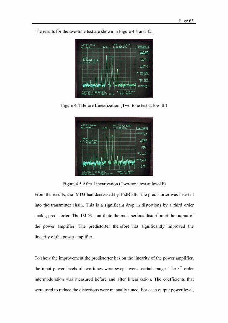
The results for the two-tone test are shown in Figure 4.4 and 4.5.
Figure 4.4 Before Linearization (Two-tone test at low-IF)
Figure 4.5 After Linearization (Two-tone test at low-IF) From the results, the IMD3 had decreased by 16dB after the predistorter was inserted
into the transmitter chain. This is a significant drop in distortions by a third order
analog predistorter. The IMD3 contribute the most serious distortion at the output of
the power amplifier. The predistorter therefore has significantly improved the
linearity of the power amplifier.
To show the improvement the predistorter has on the linearity of the power amplifier,
the input power levels of two tones were swept over a certain range. The 3rd order
intermodulation was measured before and after linearization. The coefficients that
were used to reduce the distortions were manually tuned. For each output power level,
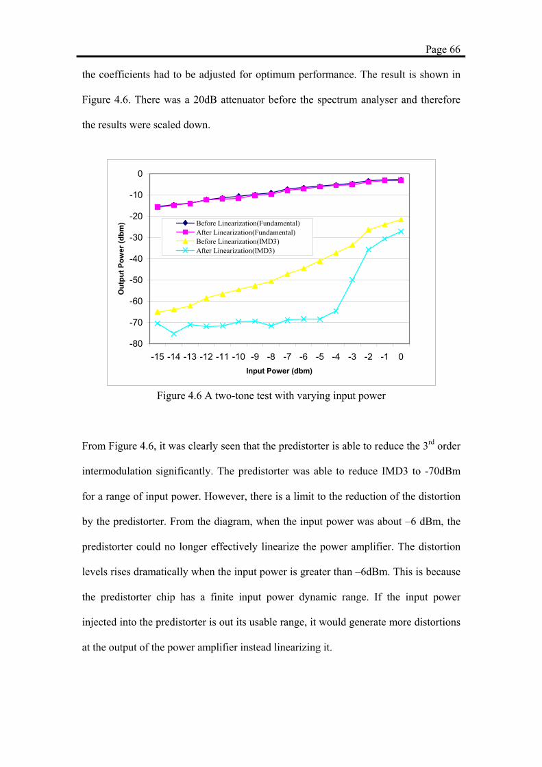
Page 66
the coefficients had to be adjusted for optimum performance. The result is shown in
Figure 4.6. There was a 20dB attenuator before the spectrum analyser and therefore
the results were scaled down.
-80
-70
-60
-50
-40
-30
-20
-10
0
-15 -14 -13 -12 -11 -10 -9 -8 -7 -6 -5 -4 -3 -2 -1 0Input Power (dbm)
Out
put P
ower
(dbm
) Before Linearization(Fundamental)After Linearization(Fundamental)Before Linearization(IMD3)After Linearization(IMD3)
Figure 4.6 A two-tone test with varying input power
From Figure 4.6, it was clearly seen that the predistorter is able to reduce the 3rd order
intermodulation significantly. The predistorter was able to reduce IMD3 to -70dBm
for a range of input power. However, there is a limit to the reduction of the distortion
by the predistorter. From the diagram, when the input power was about –6 dBm, the
predistorter could no longer effectively linearize the power amplifier. The distortion
levels rises dramatically when the input power is greater than –6dBm. This is because
the predistorter chip has a finite input power dynamic range. If the input power
injected into the predistorter is out its usable range, it would generate more distortions
at the output of the power amplifier instead linearizing it.

Page 67
Similar work done in analog predistorter [19][22][30], has used the two-tone test as
the basic test for the linearity of the power amplifier. They have shown to be able to
reduce the IMD3 from the power amplifier by 30dB using a fifth order complex
analog predistorter. From Figure 4.5, the third order complex analog predistorter that
was designed could reduce the IMD3 by more than 20dB. This suppression could be
enough for some types of power amplifier to meet its specifications. Also IMD3 is the
most serious distortion for most power amplifiers. The number of circuits required for
a third order complex analog predistortion is definitely lesser, generating lower noise
and using lesser current. The predistorter implemented by [19][22][30] did not give
results using an actual RF power amplifier. [19] and [30] has shown its results at an IF
of 200Mhz and [22] was tested at 21.4Mhz. The distortion for an actual RF power
amplifier would be more serious than low frequency amplifiers. A summary of the
two-tone test by [19][22][30] is given in Table 4.2. However in this design, it is not
possible to reduce the IMD5 of the power amplifier.
IMD Reduction Remarks [19] IMD3 Reduction: >30dB
IMD5 Reduction: 10dB The amplifier was a Class A amplifier operating at 200Mhz
[22] IMD3 Reduction:30dB IMD5 Reduction:10dB
The result was for an amplifier operating in Class AB mode at 21.4Mhz.
[30] IMD3 Reduction:>30dB IMD5 Reduction:5dB
The amplifier was a Class A amplifier operating at 200Mhz
Current Work IMD3 Reduction: 27dB An actual RF power amplifier was used. The amplifer is a Class AB power amplifer operating at 1.83Ghz.
Table 4.2 Comparison of two-tone test results performed by different design
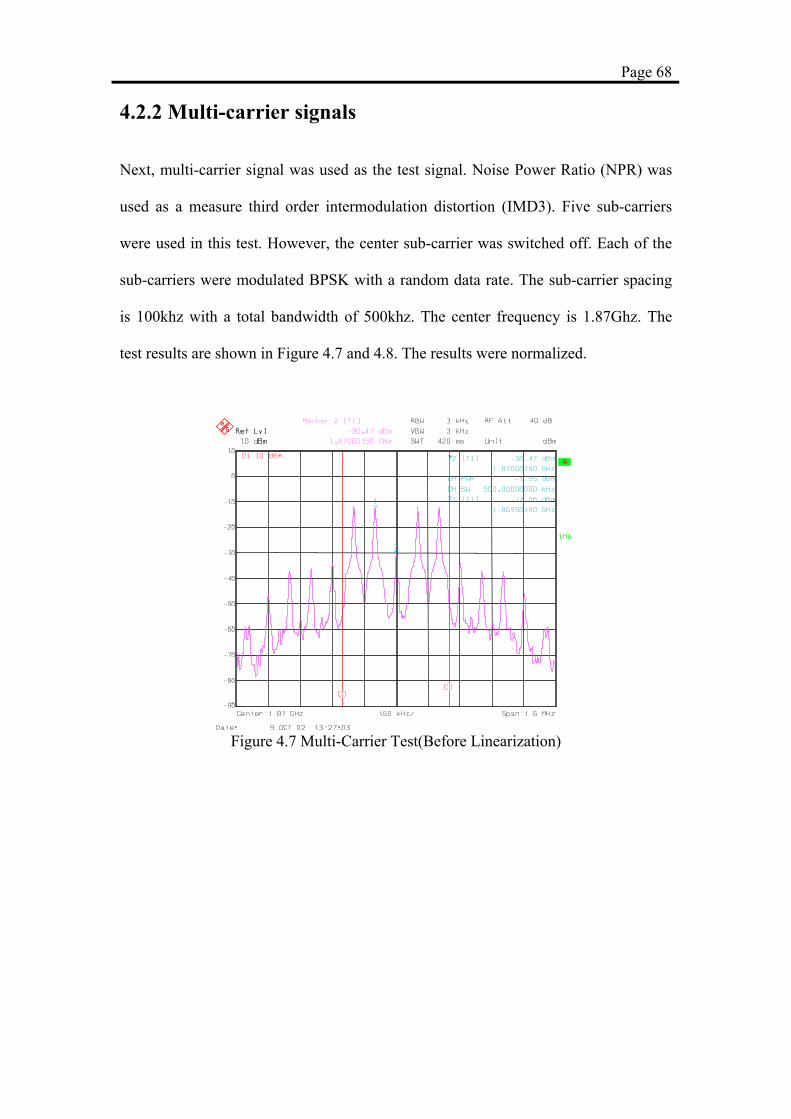
Page 68
4.2.2 Multi-carrier signals Next, multi-carrier signal was used as the test signal. Noise Power Ratio (NPR) was
used as a measure third order intermodulation distortion (IMD3). Five sub-carriers
were used in this test. However, the center sub-carrier was switched off. Each of the
sub-carriers were modulated BPSK with a random data rate. The sub-carrier spacing
is 100khz with a total bandwidth of 500khz. The center frequency is 1.87Ghz. The
test results are shown in Figure 4.7 and 4.8. The results were normalized.
Figure 4.7 Multi-Carrier Test(Before Linearization)

Page 69
Figure 4.8 Multi-Carrier Test(After Linearization) Before linearization, the power level of the center tone was –30.47dBm. It is shown in
Figure 4.7. Since the center sub-carrier was switched off, the power level of perfectly
linear power amplifier will be very low. But the distortions caused by the power
amplifier falls into the center switched off sub-carrier. The power level will give an
indication of the distortions by the power amplifier. After linearization, the power
level at the center sub-carrier decreased to –39.32dBm. There was a reduction in
power level of the center sub-carrier of –8.85dB after linearization.
From this test, it is shown that the complex analog predistorter is functioning. The
predistorter works with an actual modulated data instead of pure tones shown in two-
tone test. Also shown in Figure 4.7 and 4.8, most of the out of band distortions also
decreased due to the predistorter.
Page 70
4.2.3 OFDM signals The next test, the input was an Orthogonal Frequency Division Multiplexing (OFDM)
signal similar to 802.11a. It has a total of 52 sub-carriers occupying a 2Mhz
information bandwidth.
The test setup used was shown in Figure 4.3. The input signal, which has an
information bandwidth of 2Mhz, was upconverted to a low IF of 20Mhz before it was
injected into the predistorter.
One of the tests to measure the quality of the transmitted signal is Adjacent Channel
Power Rejection (ACPR). Due to the power amplifier’s non-linearity, there is spectral
regrowth. The leakage of this power to the adjacent channel will cause interference to
the adjacent channel. There are strict regulatory restrictions on this leakage of the
power. Measuring the ACPR is indication of the linearity of the power amplifier.

Page 71
Figure 4.9 Frequency spectrum at the input of the power amplifier (Before Linearization)
Figure 4.10 Frequency spectrum at the ouptut of the power amplifier
(Before Linearization)

Page 72
Figure 4.11 Frequency spectrum at the input of the power amplifier (After Linearization)
Figure 4.12 Frequency spectrum at the output of the power amplifier (After Linearization)

Page 73
Figures 4.9 and 4.10 shows the input and output of the power amplifier before
linearization respectively. At output of the power amplifier, there was a 20dB
attenuator. Figure 4.11 and 4.12 shows the input and output of the power amplifier
respectively after the predistorter was added. Before linearization, the ACPR before
linearization was 30.00dB. After linearization, the ACPR improves to 35.47dB.
Therefore there was an improvement of 5.47dB.
Shown also in the results, Figures 4.9 and 4.11, are the frequency spectrum at the
input of the power amplifier before and after linearization. From the two frequency
spectrums, the predistorter will generate additional third order frequency components
as predicted in chapter 3. These extra frequency components will cancel the third
order frequency components generated by the power amplifier.
4.2.4 IS95 In the final test for low-IF linearization, the input signal was generated base on the
standard IS95. It is cellular standard used in US. It uses code division multiple access
(CDMA). The input signal has a high peak-to-average of about 10dB. The modulation
used in the standard is QPSK. The bandwidth of the signal is 1.25Mhz. The center
frequency of the transmitted signal is 1.83Ghz.

Page 74
4.13 IS95 signals (Before Linearization)
4.14 IS95 signals (After Linearization)

Page 75
The frequency spectrum of the power amplifier before and after linearization is
applied is shown in Figures 4.13 and 4.14. There is a 20dB attenuator at the output of
the power amplifier to protect the inputs to the spectrum analyser. The ACPR before
linearization is 36.18dB. After linearization, the ACPR improves to 38.9dB. There is
improvement of 2.72dB only. Compared to the work in [30] which uses a 5th order
complex analog polynomial, the results does not present significant improvement. But
the results presented in [30] were obtained at an IF of 200Mhz using a Class A
amplifier. The power amplifier that was used in our test, RF Micro Devices’s RF2161,
is biased as a Class AB power amplifier operating at 1.83Ghz. It is actual power
amplifier used and it generates higher levels of distortions compared to [30]. Adaptive
linearization could be used to tune the coefficients of the predistorter [31] for
optimum performance of the power amplifier due to environmental and stimulus
change. But it is beyond the scope of current work.
4.3 Baseband analog predistortion The predistorter was then moved to the baseband level after the digital to analogue
(DAC) converter. At this position of the transmitter chain, the predistorter could
potentially perform better than IF. The design of predistorter will be simpler as the
bandwidth requirements are lower. Also there is a trend towards a zero-IF transmitter
architecture design. In order words, there are no IF stage in the transmitter. After the
DAC, I and Q channels will be modulated and upconverted to the desired RF
frequency. Therefore the only place where the analogue predistorter could be used is
at the baseband.
Page 76
A modified two-tone test was first performed. Two tones are injected into both I and
Q channels. The frequency spacing between the two tones is quite narrow (100Khz in
this case). But the two tones are located at 1Mhz and 1.1Mhz. This is done so that it is
possible to observe the harmonic and even order distortions generated by the
predistorter. These harmonic and even order distortions could be filtered out when the
predistorter is at the IF stage. But when the predistorter is placed at the baseband
level, these distortions falls in band and could not be filtered out. These distortions
will generate more distortions to the power amplifier. At the output of the RF power
amplifier, it has four tones. The test set up is shown in Figure 4.15.
Signal Source Predistorter RFAmplifier
SpectrumAnalyser
90 degreePhase shifter
4.15 Test setup of baseband predistortion

Page 77
4.16 Overall output spectrum for baseband predistortion two-tone test (before linearization)
4.17 Zooming on the frequency spectrum around the two tone for baseband predistortion two-tone test (before linearization)
Page 78
2nd order distortions
4.18 Overall output spectrum for baseband predistortion two-tone test
(after linearization)
4.19 Zooming on the frequency spectrum around the two tones for baseband predistortion two-tone test (after linearization)

Page 79
The results are shown in Figure 4.16 to 4.19. Figures 4.16 and 4.18 shows the whole
frequency spectrum at the output of the power amplifier before and after linearization
was applied respectively. There was a 20dB attenuator before the spectrum analyser.
Figures 4.17 and 4.19 look at the frequency spectrum around the two tones on upper
side band before and after linearization was applied respectively. From 4.17 and 4.19,
the IMD3 was reduced from –45dBm to –65dBm. That is a reduction of 20dB in
IMD3. It shows that the predistorter was reducing the third order distortions generated
by the power amplifier. One interesting observation is that the IMD5 had also reduced
by about 2dB after linearization was applied.
However, comparing the overall frequency spectrum shown in Figures 4.16 and 4.18,
there were extra frequency distortions at the output of the power amplifier after
adding the predistorter. These extra frequency components were the second order
distortions generated by the predistorter. The power levels of these second order
distortions were around –32dBm. The second order distortions were due to the device
mismatch, d.c offsets etc. These second order distortions generated by the predistorter
could not be filtered out when the predistorter operates at the baseband. The work
done L. Sundström and Timo Rahkonen [19][22][30] had not shown results when
their complex analog predistorter is working at the baseband with a RF power
amplifier. This is the first time these results are reported. Second order distortions
could be reduced by paying close attention to matching of the transistors in analog
multipliers. If the analog multipliers were mismatched, second order distortions will
appear at the output of the predistorter. It is possible to reduce the second order
distortions but not entirely eliminate it. This is because the matching of the transistor
is partly process dependant and the wafer plant could not guarantee perfect matching.

Page 80
4.4 Analog predistortion for Radio Over Fiber System (ROF)
The predistorter was then used to linearize a non-linear optical system. There is
currently active research to transmit radio signals over optical fiber. Transmitting
radio signals over optical fiber has the potential to reduce the overall costs of the
installation of cellular systems [32]. In the optical system, it consists of the electrical-
to-optical circuits, optical laser, photo detector, optical-to-electrical-circuits etc. The
system exhibited characteristics similar to the power amplifier. When two tones were
send into the system, the output seen from the spectrum analyser has 3rd order
intermodulation distortions. Therefore the predistorter was used to linearize the
optical system. The test set up is shown in Figure 4.20.
Signal Source PredistorterLaserDiode
Fibre Optics
PhotoDetector
SpectrumAnalyser
Optical System
RF Output
RF Input
BasebandModulator
Figure 4.20 Test Setup using predistorter in Radio Over Fiber system The same modified two-tones test used in Section 4.2 was used in this test. The
transmitted RF frequency is 2.5Ghz. The two tones injected into the I and Q channel
were 1.45Mhz and 1.55Mhz with a frequency spacing of 100khz apart. The results are
shown in Figures 4.19 to 4.22.

Page 81
4.21 Overall output spectrum for ROF predistortion two-tones test (before linearization)
4.22 Zooming on the frequency spectrum around the two tones for ROF predistortion
two-tones test (before linearization)

Page 82
2nd order distortions
4.23 Overall output spectrum for ROF predistortion two-tones test (after linearization)
4.24 Zooming on the frequency spectrum around the two tones for ROF predistortion
two-tones test (after linearization)

Page 83
The results in Figures 4.21 and 4.23 shows overall spectrum at the output of the ROF
system. Comparing the two figures, there were additional frequency components
generated by the predistorter. This was expected as stated in previous section 4.2.
These distortions were the second order distortions generated by the predistorter. The
power levels of these second order distortions were around –45dBm. Looking
specifically at the two tones, shown in Figures 4.22 and 4.24, the IMD3 generated was
reduced from –51dBm to –67dBm. It was a reduction of 16dB due to the predistorter.
This demonstrates that the predistorter is able to reduce the distortions generated by
the ROF system.
The same two-tones test was repeated for different input power level. The distortions
caused by the IMD3 were recorded before and after the predistorter was added. The
output power was normalised. The results are shown in Figure 4.25.
-80
-70
-60
-50
-40
-30
-20
-10
0
-12
-11
-10 -9 -8 -7 -6 -5 -4 -3 -2 -1 0
Input Power(dbm)
Out
put P
ower
(dbm
)
Output Power of 2 Tones
Before Lineaization(IMD3)After Linearization(IMD3)
Figure 4.25 Two-tones test for ROF system

Page 84
From the results, the predistorter is able to reduce the distortions such that the power
level of the IMD3 is below -60dBm. This is a significant reduction in IMD3 with the
predistorter. There is only a single input power point, at -9dBm, that the predistorter is
unable to decrease the IMD3. It might be due to some other anomalies operating in
either the laser diode or photodiode that is not present in the power amplifier.
The test was repeated again but instead of two tones a multi-carrier modulated signal
was used as the input. The frequencies of the sub-carriers were carefully selected so
the frequencies of each sub-carrier at the baseband must not coincide with its 2nd order
distortions. The test setup was the same as two-tone test. The center carrier frequency
is 2.5Ghz. There were five sub-carrier with the center carrier switched off and each
was modulated with QPSK. The sub-carrier frequency spacing is 100khz and total
bandwidth is 500khz. The results are shown in Figures 4.24 and 4.25. The total
spectrum had a low and upper frequency side band similar to the overall output
spectrum for the two-tones test. Figures 4.26 and 4.27 shows only the lower side
band.
Page 85
Out of Band Distortions Out of Band Distortions
4.26 Multi-Carrier Test for ROF system(Before Linearization)
Out of Band Distortions Out of Band Distortions
4.27 Multi-Carrier Test for ROF system(After Linearization)

Page 86
From the results shown in Figures 4.26 and 4.27, the power level of the center tone
was reduced from –34.72dBm to –41.11dBm. The filling up of the center switched off
carrier gives an indication of the distortion caused by the ROF system. It shows that
the predistorter is able to reduce the distortions by 6.39dB. Another observation was
that the out of band distortions were also reduced. In one of the out of band
distortions, pointed by an arrow in Figures 4.24 and 4.25, the power level of the
distortion drops from –37.5dBm to -43.75dBm. That is a reduction of 6.25dB. The
distortion levels of the most serious distortions had decreased after linearization.
In this series of tests using the ROF system, it shows that the predistorter could be
extended to be use in the ROF system. The predistorter could reduce the IMD3 caused
by the ROF systems.

Chapter 5
Conclusions
The power amplifier is a critical component in the transceiver. The power amplifiers
suffers from both amplitude and phase distortions. It could be modelled using a
complex odd order polynomial. However, the third order distortion is the most serious
distortion generated by the power amplifier. This is even more dominant in a multi-
carrier system. In order to properly give a qualitative measure of the linearity of the
power amplifier, different tests are introduced such as the two-tone test, Noise Power
Ratio (NPR), Adjacent Power Rejection Ratio (ACPR). To improve the linearity of
the power amplifier, three different general methods were mentioned, the Cartesian
feedback, feedfoward and predistortion.
In this thesis, the work was presented on linearizing the power amplifier using
predistortion techniques. The predistorter could be implemented at different stages in

Page 88
the transmitter chain. The predistorter implemented was a third order analog complex
predistorter that could operate in the baseband and low-IF reducing the third order
distortions from the power amplifier. One of the main blocks in the predistorter is the
analog multiplier. An improved analog multiplier was introduced. Addition operation
could be done by tying the outputs of two multipliers together. The load of the
multiplier is diode connected MOS. It resistance is increased using positive feedback.
The blocks of the predistorter are the transconductor, transimpedance cells and output
buffers. It was fabricated in 0.8µm SiGe BiCMOS.
In the tests for the predistorter chip, an actual RF power amplifier was used. In the
two-tone test at low-IF, the predistorter had been able to reduce the third order
intermodulation distortion significantly. Different test signals such as multi-carrier,
OFDM had been used to inject into the predistorter. Using different metrics for the
linearity of the power amplifier, such as NPR and ACPR, the predistorter had been
shown to reduce the distortions caused by the power amplifier.
In the baseband predistorter, the predistorter was shown to reduce the distortions
caused by the power amplifier. However, due to the unwanted distortions generated
by the predistorter, second order distortions could be observed at the output of the
power amplifier.
The predistorter was extended to be use in the Radio Over Fiber system. The
characteristic of the system is similar to the power amplifier. In the testing, the
predistorter was shown to reduce the distortions caused by the system.

Page 89
Therefore, the third order analog complex predistorter is able to reduce the distortions
of the power amplifier, improving its linearity. This would allow the power amplifier
to operate at higher power efficiency. The use of the predistorter had been extended to
ROF system. This raises the possibility of using the predistorter in other areas.

Bibliography
[1] Behzad Razavi, “RF Microelectronics”, Prentice Hall, 1st edition, 1997
[2] Raab, F.H.; Asbeck, P.; Cripps, S.; Kenington, P.B.; Popovic, Z.B.; Pothecary
N.; Sevic, J.F.; Sokal, N.O, “Power amplifiers and transmitters for RF and
microwave”, IEEE Trans. on Microwave Theory and Techniques, Vol. 50
Issue 3, Mar 2002, pp. 814 -826
[3] Chris Toumazou and George Moschytz, “Trade-Offs in Analog Circuit
Design”, Kluwer Academic Publishers ,2002
[4] RF Micro Devices, Part No. RF2161, www.rfmd.com
[5] Raytheon, Part No. RMPA5251-251, www.raytheonrf.com
[6] Nathan O. Sakal and Alan D. Sokal, “Class E – A New Class of High-
Efficiency Tuned single-Ended Switching Power Amplifiers”, IEEE Journal
of Solid State Circuits, Vol. 10, pp. 168-175, June 1975
[7] Peter B. Kenington, “High Linearity RF Amplifier Design”, Artech Hous,2000
[8] Steve C. Cripps, “RF Power Amplifiers for Wireless Communications”,
Artech House,1999

Page 91
[9] Joel H. K. Vuolei, Timo Rahkonen and Jani P. A. Manninen, “Measurements
Technique for Characterizing Memory Effects in RF Power Amplifiers”, IEEE
Trans. on Microwave Theory and Tecniques, Vol. 49, No. 8, August 2001, pp.
1383-1389
[10] Joel Vuolei, Timo Rahkonen and Jani Manninen, “Canceling the memory
effects in RF Power Amplifier”, ISCAS 2001, 6-9 May 2001, pp. 57 -60
[11] Steve C. Cripps, “Advanced Techniques in RF Power Amplifier Design”,
Artech House, 2002
[12] Saleh, A. A. M., “Frequency-independent and frequency-dependant non-linear
models of TWT amplifiers”, IEEE Trans. on Communications, Vol. COM-29,
November 1981, pp. 1715-1720
[13] Agilent Application Note, AN 1311, “Understanding CDMA Measurements
for Base Stations and Their Components”, Agilent Tehnologies,
www.agilent.com
[14] Back, H. S., US Patent no. 1,686,792, 9th October 1928
[15] Mats Johansson and Thomas Mattsson, “Transmitter Linearization using
Cartesian Feedback for Linear TDMA Modulation”, IEEE Vehicular
Technology Conference, 19-22 May 1991, pp. 439 –444

Page 92
[16] Nick Pothecary, “Feedfoward Linear Power Amplifiers”, Artech House, 1999
[17] James K. Cavers, “Adaptation Behavior of a Feedfoward Amplifier
Linearizer”, IEEE Trans. on Vehicular Technology, Vol. 44, No. 1, Feb. 1995,
pp. 31-40
[18] Tri T. Ha, “Digital Satellite Communications”, McGraw Hill, 1986
[19] E. Westesson, L. Sundström, “A complex polynomial predistorter chip in
CMOS for baseband or IF linearization of RF power amplifier”, ISCAS '99,
Proceedings of the 1999 IEEE International Symposium, vol. 1, Jul 1999
[20] Natasa Males-Ilic, Bratislav Milovanoic, Djuradj Budimir, “Linearization
Technique for reducing Third- ad Fifth Order Intermodulation Distortion
Products in Multichannel Amplifier”, 33rd European Microwave Conference,
Munich 2003.
[21] James K. Cavers, “Amplifier Linearization Using a Digital Predistorter with
Fast Adptation and Low Memory Requirements”, IEEE Trans. On Vehicular
Technology, vol 39, no. 4, pp. 374-382, Nov. 1990
[22] Timo Rahkonen, Tapio Kankaala, Marko Neitola and Antti Heiskanen, “Using
Analog Predistortion for Linearizing Class A-C Power Amplifiers”, Analog
Integrated Circuits and Signal Processing, 22, 1999, pp. 31-39

Page 93
[23] C. Toumazou, F.J. Lidgey & D.G. Haigh, “Analogue IC design: the current-
mode approach”, Institution of Electrical Engineers, 1993
[24] B. Gilbert, “A precision four-quadrant multiplier with subnanosecond
response,” IEEE Journal of Solid State Circuits, Vol. SC-3, pp. 353-365, Dec
1968
[25] Gunhee Han and Edgar Sánchex-Sinencio, “CMOS Transconductance
Multipliers: A Tutorial”, IEEE Trans. On Cricuits and Systems II: Analog and
Digital Signal Processing, vol 45, No 12, Dec 1998, pp. 1550-1563
[26] Behzad Razavi, “Design of Analog CMOS Integrated Circuits”, McGraw Hill,
1st Edition, 2000
[27] Mezyad Amourah and Randall Geiger, “A High Gain Strategy with positive-
feedback gain enhancement Technique”, ISCAS 2001, The 2001 IEEE
International Symposium, vol. 1, 6-9 May 2001
[28] Cadence Design Systems, “www.cadence.com”
[29] Christopher Saint and Judy Saint, “IC Mask Design, Essential Layout
Techniques”, McGraw Hill, 1st Edition, 2002

Page 94
[30] WESTESSON E and SUNDSTRÖM L.: "Low Power Complex Polynomial
Predistorter Circuit in CMOS for RF PA Linearization", Proceedings of 27th
Europe Solid State Circuits Conf. 2001
[31] Allen Katz, “Linearization: Reducing distortion in Power Amplifier”, IEEE
Microwave Magazine, Dec 2001, pp.37-49
[32] Hamed Al-Raweshidy and Shozo Komaki, “Radio Over Fiber Technologies
for Mobile Communications Networks”, Artech House, 1st Edition, 2002

Appendix Netlist of Predistorter Chip // Generated for: spectre // Generated on: Dec 13 15:28:00 2004 // Design library name: pd3 // Design cell name: pd_top1 // Design view name: schematic simulator lang=spectre global 0 include "/opt/ic/446.100.111.8/tools.sun4v/dfII/samples/artist/ahdlLib/quantity.spectre" include "/opt/process/AMS_3.40_CDS/spectre/byr/mcparams.scs" include "/opt/process/AMS_3.40_CDS/spectre/byr/cmos53.scs" section=cmostm include "/opt/process/AMS_3.40_CDS/spectre/byr/res.scs" section=restm include "/opt/process/AMS_3.40_CDS/spectre/byr/cap.scs" section=captm include "/opt/process/AMS_3.40_CDS/spectre/byr/vbic.scs" section=biptm // Library name: cartesian // Cell name: INV_PD // View name: schematic subckt INV_PD IN OUT vdd vss vtie I4 (OUT IN vss vtie) modn w=2.4u l=0.8u as=5.52e-12 ad=5.52e-12 ps=7u \ pd=7u nrd=0.541667 nrs=0.541667 ng=1 I3 (OUT IN vdd vdd) modp w=4.8u l=0.8u as=1.104e-11 ad=1.104e-11 \ ps=9.4u pd=9.4u nrd=0.270833 nrs=0.270833 ng=1 ends INV_PD // End of subcircuit definition. // Library name: cartesian // Cell name: npnx10_bandgap // View name: schematic subckt npnx10_bandgap B C E SUB I8 (C B E SUB) npn111 area=2 m=1 I9 (C B E SUB) npn111 area=2 m=1 I10 (C B E SUB) npn111 area=2 m=1 I7 (C B E SUB) npn111 area=2 m=1 I6 (C B E SUB) npn111 area=2 m=1 I5 (C B E SUB) npn111 area=2 m=1 I3 (C B E SUB) npn111 area=2 m=1 I4 (C B E SUB) npn111 area=2 m=1 I2 (C B E SUB) npn111 area=2 m=1

Page 96
I1 (C B E SUB) npn111 area=2 m=1 ends npnx10_bandgap // End of subcircuit definition. // Library name: SCHEMA // Cell name: cpolybr3 // View name: schematic subckt cpolybr3 PLUS MINUS REF parameters area=100p perimeter=40u np=1 csub=1f rsub=1 rp1=1 rp2=1 CP1B (top bottom) cpolyb area=area perimeter=perimeter m=np C11 (bottom int3) capacitor c=csub m=np R12 (int3 REF) resistor r=rsub m=np RP1 (bottom MINUS) resistor r=rp1 m=np RPB (PLUS top) resistor r=rp2 m=np ends cpolybr3 // End of subcircuit definition. // Library name: cartesian // Cell name: bandgap // View name: schematic subckt bandgap PD ibg_1mI_0 ibg_1mQ_0 ibg_2mI_0 ibg_2mQ_0 ibg_50uI_0 \ ibg_50uI_1 ibg_50uQ_0 ibg_50uQ_1 vbg_fb vbg_out1 vbg_out2 vdda \ vssa vtie I1 (PD PDb vdda vssa vtie) INV_PD Q2 (net451 net449 net260 vtie) npnx10_bandgap Q15 (vbg_fb net198 net266 vtie) npnx10_bandgap C0 (net406 vssa vtie) cpolybr3 area=5.61516e-09 perimeter=305.802u \ np=1 csub=462.823f rsub=100 rp1=12.0278 rp2=47.2345 C2 (ibg_i vssa vtie) cpolybr3 area=5.61516e-09 perimeter=305.802u np=1 \ csub=462.823f rsub=100 rp1=12.0278 rp2=47.2345 C1 (net190 vssa vtie) cpolybr3 area=1.11454e-09 perimeter=136.301u \ np=1 csub=113.897f rsub=100 rp1=6.14195 rp2=47.1873 I120 (net215 PD vssa vtie) modn w=2u l=0.8u as=4.6e-12 ad=4.6e-12 \ ps=6.6u pd=6.6u nrd=0.65 nrs=0.65 ng=1 I121 (vbg_fb PD vssa vtie) modn w=2u l=0.8u as=4.6e-12 ad=4.6e-12 \ ps=6.6u pd=6.6u nrd=0.65 nrs=0.65 ng=1 M1 (net222 net222 vssa vtie) modn w=2u l=120u as=4.6e-12 ad=4.6e-12 \ ps=6.6u pd=6.6u nrd=0.65 nrs=0.65 ng=1 M19 (BG_GEN PD vssa vtie) modn w=2u l=0.8u as=4.6e-12 ad=4.6e-12 \ ps=6.6u pd=6.6u nrd=0.65 nrs=0.65 ng=1 M9 (net231 net359 net232 vtie) modn w=80u l=2u as=1.84e-10 ad=1.84e-10 \ ps=84.6u pd=84.6u nrd=0.01625 nrs=0.01625 ng=1 M10 (net332 BG_GEN net232 vtie) modn w=80u l=2u as=1.84e-10 \ ad=1.84e-10 ps=84.6u pd=84.6u nrd=0.01625 nrs=0.01625 ng=1 M20 (ibg_out1 BG_GEN vbg_out1 vtie) modn w=200u l=2u as=4.6e-10 \ ad=4.6e-10 ps=204.6u pd=204.6u nrd=0.0065 nrs=0.0065 ng=1 RD1 (vtie net210) rpoly2 w=6u l=25.8u m=1 R15 (vtie net200) rpoly2 w=6u l=25.8u m=1 R26 (net248 vssa) rpoly2 w=6u l=77.4u m=1 R27 (net248 vssa) rpoly2 w=6u l=77.4u m=1 R23 (net250 vssa) rpoly2 w=6u l=77.4u m=1 R24 (net248 vssa) rpoly2 w=6u l=77.4u m=1 R29 (vtie net509) rpoly2 w=6u l=77.4u m=1 R30 (vtie net510) rpoly2 w=6u l=77.4u m=1 R28 (ibg_i vssa) rpoly2 w=6u l=1856.000u m=1 R25 (net248 vssa) rpoly2 w=6u l=77.4u m=1

Page 97
R2 (net258 vssa) rpoly2 w=6u l=309.4u m=1 R1 (net260 vssa) rpoly2 w=6u l=102.9u m=1 R22 (net252 vssa) rpoly2 w=6u l=77.4u m=1 R5 (BG_STAB net190) rpoly2 w=6u l=580.00000u m=1 R4 (BG_COM vssa) rpoly2 w=6u l=313.2u m=1 R3 (net266 BG_COM) rpoly2 w=6u l=102.9u m=1 I142 (ibg_out1 ibg_out1 vdda vdda) modp w=50u l=2u as=1.15e-10 \ ad=1.15e-10 ps=54.6u pd=54.6u nrd=0.026 nrs=0.026 ng=1 I161 (ibg_i ibg_out1 vdda vdda) modp w=50u l=2u as=1.15e-10 \ ad=1.15e-10 ps=54.6u pd=54.6u nrd=0.026 nrs=0.026 ng=1 I173 (ibg_out2 ibg_out2 vdda vdda) modp w=500u l=2u as=1.15e-09 \ ad=1.15e-09 ps=504.6u pd=504.6u nrd=0.0026 nrs=0.0026 ng=1 I168 (ibg_2mQ_0 ibg_out2 vdda vdda) modp w=500u l=2u as=1.15e-09 \ ad=6.5e-10 ps=504.6u pd=2.6u nrd=0.0026 nrs=0.0026 ng=2 I175 (ibg_out2 PDb vdda vdda) modp w=40u l=0.8u as=9.2e-11 ad=9.2e-11 \ ps=44.6u pd=44.6u nrd=0.0325 nrs=0.0325 ng=1 I165 (net390 net390 vdda vdda) modp w=100u l=2u as=2.3e-10 ad=2.3e-10 \ ps=104.6u pd=104.6u nrd=0.013 nrs=0.013 ng=1 I199 (ibg_50uI_0 ibg_out1 vdda vdda) modp w=50u l=2u as=1.15e-10 \ ad=1.15e-10 ps=54.6u pd=54.6u nrd=0.026 nrs=0.026 ng=1 I200 (ibg_50uQ_0 ibg_out1 vdda vdda) modp w=50u l=2u as=1.15e-10 \ ad=1.15e-10 ps=54.6u pd=54.6u nrd=0.026 nrs=0.026 ng=1 I163 (net406 net390 vdda vdda) modp w=100u l=2u as=2.3e-10 ad=2.3e-10 \ ps=104.6u pd=104.6u nrd=0.013 nrs=0.013 ng=1 I167 (ibg_50uQ_1 ibg_out1 vdda vdda) modp w=50u l=2u as=1.15e-10 \ ad=1.15e-10 ps=54.6u pd=54.6u nrd=0.026 nrs=0.026 ng=1 I164 (net390 PDb vdda vdda) modp w=4u l=0.8u as=9.2e-12 ad=9.2e-12 \ ps=8.6u pd=8.6u nrd=0.325 nrs=0.325 ng=1 I181 (net435 ibias_out vdda vdda) modp w=25u l=2u as=5.75e-11 \ ad=5.75e-11 ps=29.6u pd=29.6u nrd=0.052 nrs=0.052 ng=1 M4 (net331 PD vdda vdda) modp w=2u l=1u as=4.6e-12 ad=4.6e-12 ps=6.6u \ pd=6.6u nrd=0.65 nrs=0.65 ng=1 M3 (net215 net222 net331 net331) modp w=5u l=1u as=1.15e-11 \ ad=1.15e-11 ps=9.6u pd=9.6u nrd=0.26 nrs=0.26 ng=1 I197 (ibg_1mI_0 ibg_out2 vdda vdda) modp w=500u l=2u as=1.15e-09 \ ad=1.15e-09 ps=504.6u pd=504.6u nrd=0.0026 nrs=0.0026 ng=1 I198 (ibg_1mQ_0 ibg_out2 vdda vdda) modp w=500u l=2u as=1.15e-09 \ ad=1.15e-09 ps=504.6u pd=504.6u nrd=0.0026 nrs=0.0026 ng=1 M2 (net222 net332 vdda vdda) modp w=50u l=2u as=1.15e-10 ad=1.15e-10 \ ps=54.6u pd=54.6u nrd=0.026 nrs=0.026 ng=1 M11 (net231 net231 vdda vdda) modp w=10u l=2u as=2.3e-11 ad=2.3e-11 \ ps=14.6u pd=14.6u nrd=0.13 nrs=0.13 ng=1 M8 (net332 net332 vdda vdda) modp w=10u l=2u as=2.3e-11 ad=2.3e-11 \ ps=14.6u pd=14.6u nrd=0.13 nrs=0.13 ng=1 I171 (net626 net546 vdda vdda) modp w=25u l=2u as=3.60714e-11 \ ad=3.60714e-11 ps=6.45714u pd=6.45714u nrd=0.052 nrs=0.052 ng=7 M5 (net215 ibias_out vdda vdda) modp w=25u l=2u as=5.75e-11 \ ad=5.75e-11 ps=29.6u pd=29.6u nrd=0.052 nrs=0.052 ng=1 I193 (ibg_2mI_0 ibg_out2 vdda vdda) modp w=500u l=2u as=1.15e-09 \ ad=6.5e-10 ps=504.6u pd=2.6u nrd=0.0026 nrs=0.0026 ng=2 I196 (ibg_50uI_1 ibg_out1 vdda vdda) modp w=50u l=2u as=1.15e-10 \ ad=1.15e-10 ps=54.6u pd=54.6u nrd=0.026 nrs=0.026 ng=1 M22 (ibg_out1 PDb vdda vdda) modp w=2u l=0.8u as=4.6e-12 ad=4.6e-12 \ ps=6.6u pd=6.6u nrd=0.65 nrs=0.65 ng=1 M13 (ibias_out PDb vdda vdda) modp w=2u l=0.8u as=4.6e-12 ad=4.6e-12 \ ps=6.6u pd=6.6u nrd=0.65 nrs=0.65 ng=1 M7 (net459 net459 net359 net359) modp w=15u l=1u as=3.45e-11 \

Page 98
ad=3.45e-11 ps=19.6u pd=19.6u nrd=0.0866667 nrs=0.0866667 ng=1 M6 (net359 ibias_out vdda vdda) modp w=5u l=2u as=1.15e-11 ad=1.15e-11 \ ps=9.6u pd=9.6u nrd=0.26 nrs=0.26 ng=1 M17 (BG_STAB net231 vdda vdda) modp w=20u l=2u as=4.6e-11 ad=4.6e-11 \ ps=24.6u pd=24.6u nrd=0.065 nrs=0.065 ng=1 M12 (ibias_out ibias_out vdda vdda) modp w=25u l=2u as=5.75e-11 \ ad=5.75e-11 ps=29.6u pd=29.6u nrd=0.052 nrs=0.052 ng=1 M14 (BG_GEN ibias_out vdda vdda) modp w=25u l=2u as=4.3125e-11 \ ad=2.875e-11 ps=15.95u pd=2.3u nrd=0.052 nrs=0.052 ng=4 M18 (vssa BG_STAB BG_GEN BG_GEN) modp w=120u l=2u as=2.76e-10 \ ad=2.76e-10 ps=124.6u pd=124.6u nrd=0.0108333 nrs=0.0108333 ng=1 M16 (BG_STAB net198 BG_GEN BG_GEN) modp w=60u l=2u as=1.38e-10 \ ad=1.38e-10 ps=64.6u pd=64.6u nrd=0.0216667 nrs=0.0216667 ng=1 M15 (net198 net198 BG_GEN BG_GEN) modp w=60u l=2u as=1.38e-10 \ ad=1.38e-10 ps=64.6u pd=64.6u nrd=0.0216667 nrs=0.0216667 ng=1 Q3 (ibias_out net215 net449 vtie) npn111 area=2 m=1 Q16 (BG_STAB vbg_fb BG_COM vtie) npn111 area=2 m=1 I189 (net390 ibg_i net389 vtie) npn111 area=2 m=1 I177 (ibg_out2 net406 vbg_out2 vtie) npn111 area=2 m=1 I178 (net389 net433 net248 vtie) npn111 area=2 m=1 I176 (ibg_out2 net406 vbg_out2 vtie) npn111 area=2 m=1 I185 (net433 net433 net250 vtie) npn111 area=2 m=1 I180 (vdda net435 net433 vtie) npn111 area=2 m=1 I126 (net427 net203 net211 vtie) npn111 area=2 m=1 I127 (net431 net202 net201 vtie) npn111 area=2 m=1 I179 (net435 net433 net252 vtie) npn111 area=2 m=1 Q5 (net232 net451 net258 vtie) npn111 area=2 m=1 I128 (net443 net207 net212 vtie) npn111 area=2 m=1 I125 (net447 net205 net209 vtie) npn111 area=2 m=1 Q0 (net451 net449 vssa vtie) npn111 area=2 m=1 Q1 (net215 net215 net451 vtie) npn111 area=2 m=1 I190 (net406 vbg_out2 net389 vtie) npn111 area=2 m=1 Q4 (net459 net459 vssa vtie) npn111 area=2 m=1 ends bandgap // End of subcircuit definition. // Library name: pd3 // Cell name: output_buffer // View name: schematic subckt output_buffer Iin\+ Iin\- Vout\+ Vout\- Vref vdd vss vtie i_1mA I54 (Vout\- net051 vss vtie) npn112 area=4 m=1 I49 (Vout\+ net051 vss vtie) npn112 area=4 m=1 I48 (vdd net30 Vout\+ vtie) npn111 area=2 m=1 I51 (vdd i_1mA net051 vtie) npn111 area=2 m=1 I55 (vdd net031 Vout\- vtie) npn111 area=2 m=1 I50 (i_1mA net051 vss vtie) npn111 area=2 m=1 I13 (Iin\+ Iin\+ vss vtie) modn w=8u l=2u as=1.84e-11 ad=1.84e-11 \ ps=12.6u pd=12.6u nrd=0.1625 nrs=0.1625 ng=1 I14 (Iin\- Iin\- vss vtie) modn w=8u l=2u as=1.84e-11 ad=1.84e-11 \ ps=12.6u pd=12.6u nrd=0.1625 nrs=0.1625 ng=1 I16 (Iin\- Vref vdd vdd) modp w=65u l=2u as=1.495e-10 ad=1.495e-10 \ ps=69.6u pd=69.6u nrd=0.02 nrs=0.02 ng=1 I19 (vss Iin\+ net30 net30) modp w=20u l=2u as=4.6e-11 ad=4.6e-11 \ ps=24.6u pd=24.6u nrd=0.065 nrs=0.065 ng=1 I21 (net031 Vref vdd vdd) modp w=100u l=2u as=2.3e-10 ad=2.3e-10 \ ps=104.6u pd=104.6u nrd=0.013 nrs=0.013 ng=1 I22 (net30 Vref vdd vdd) modp w=100u l=2u as=2.3e-10 ad=2.3e-10 \

Page 99
ps=104.6u pd=104.6u nrd=0.013 nrs=0.013 ng=1 I20 (vss Iin\- net031 net031) modp w=20u l=2u as=4.6e-11 ad=4.6e-11 \ ps=24.6u pd=24.6u nrd=0.065 nrs=0.065 ng=1 I15 (Iin\+ Vref vdd vdd) modp w=65u l=2u as=1.495e-10 ad=1.495e-10 \ ps=69.6u pd=69.6u nrd=0.02 nrs=0.02 ng=1 ends output_buffer // End of subcircuit definition. // Library name: pd3 // Cell name: balanced_diff_current // View name: schematic subckt balanced_diff_current Iin\+ Iin\- Iout\+ Iout\- vdd vss vtie I38 (net70 net70 vdd vdd) modp w=50u l=2u as=1.15e-10 ad=1.15e-10 \ ps=54.6u pd=54.6u nrd=0.026 nrs=0.026 ng=1 I31 (Iout\- net70 vdd vdd) modp w=50u l=2u as=1.15e-10 ad=1.15e-10 \ ps=54.6u pd=54.6u nrd=0.026 nrs=0.026 ng=1 I5 (Iout\+ net82 vdd vdd) modp w=50u l=2u as=1.15e-10 ad=1.15e-10 \ ps=54.6u pd=54.6u nrd=0.026 nrs=0.026 ng=1 I4 (net82 net82 vdd vdd) modp w=50u l=2u as=1.15e-10 ad=1.15e-10 \ ps=54.6u pd=54.6u nrd=0.026 nrs=0.026 ng=1 I3 (Iout\- Iin\+ vss vtie) modn w=25u l=2u as=5.75e-11 ad=5.75e-11 \ ps=29.6u pd=29.6u nrd=0.052 nrs=0.052 ng=1 I12 (net70 Iin\- vss vtie) modn w=25u l=2u as=5.75e-11 ad=5.75e-11 \ ps=29.6u pd=29.6u nrd=0.052 nrs=0.052 ng=1 I33 (Iout\+ Iin\- vss vtie) modn w=25u l=2u as=5.75e-11 ad=5.75e-11 \ ps=29.6u pd=29.6u nrd=0.052 nrs=0.052 ng=1 I2 (Iin\+ Iin\+ vss vtie) modn w=25u l=2u as=5.75e-11 ad=5.75e-11 \ ps=29.6u pd=29.6u nrd=0.052 nrs=0.052 ng=1 I1 (net82 Iin\+ vss vtie) modn w=25u l=2u as=5.75e-11 ad=5.75e-11 \ ps=29.6u pd=29.6u nrd=0.052 nrs=0.052 ng=1 I0 (Iin\- Iin\- vss vtie) modn w=25u l=2u as=5.75e-11 ad=5.75e-11 \ ps=29.6u pd=29.6u nrd=0.052 nrs=0.052 ng=1 ends balanced_diff_current // End of subcircuit definition. // Library name: pd3 // Cell name: pd_output_top // View name: schematic subckt pd_output_top Iin\+ Iin\- Vout\+ Vout\- Vref vdd vss vtie i_1mA I8 (net022 net021 Vout\+ Vout\- Vref vdd vss vtie i_1mA) output_buffer I6 (Iin\+ Iin\- net022 net021 vdd vss vtie) balanced_diff_current ends pd_output_top // End of subcircuit definition. // Library name: pd3 // Cell name: LinearRegion_MOS_Multiplier2_CoupledLoad // View name: schematic subckt LinearRegion_MOS_Multiplier2_CoupledLoad Vout\+ Vout\- Vref Vx1\+ \ Vx1\- Vx2\+ Vx2\- Vy1\+ Vy1\- Vy2\+ Vy2\- vdd vss vtie I69 (vss net0231 net0118 net0118) modp w=10u l=2u as=2.3e-11 \ ad=2.3e-11 ps=14.6u pd=14.6u nrd=0.13 nrs=0.13 ng=1 I77 (net0114 Vref vdd vdd) modp w=10u l=2u as=2.3e-11 ad=2.3e-11 \ ps=14.6u pd=14.6u nrd=0.13 nrs=0.13 ng=1 I78 (vss net096 net0114 net0114) modp w=10u l=2u as=2.3e-11 ad=2.3e-11 \ ps=14.6u pd=14.6u nrd=0.13 nrs=0.13 ng=1 I75 (net0147 Vref vdd vdd) modp w=20u l=2u as=4.6e-11 ad=4.6e-11 \ ps=24.6u pd=24.6u nrd=0.065 nrs=0.065 ng=1
Page 100
I41 (V\+ V\- vdd vdd) modp w=35u l=2u as=8.05e-11 ad=8.05e-11 ps=39.6u \ pd=39.6u nrd=0.0371429 nrs=0.0371429 ng=1 I39 (V\- V\+ vdd vdd) modp w=35u l=2u as=8.05e-11 ad=8.05e-11 ps=39.6u \ pd=39.6u nrd=0.0371429 nrs=0.0371429 ng=1 I70 (net0118 Vref vdd vdd) modp w=10u l=2u as=2.3e-11 ad=2.3e-11 \ ps=14.6u pd=14.6u nrd=0.13 nrs=0.13 ng=1 I44 (net054 Vref vdd vdd) modp w=50u l=2u as=1.15e-10 ad=1.15e-10 \ ps=54.6u pd=54.6u nrd=0.026 nrs=0.026 ng=1 I10 (V\+ V\+ vdd vdd) modp w=50u l=2u as=1.15e-10 ad=1.15e-10 ps=54.6u \ pd=54.6u nrd=0.026 nrs=0.026 ng=1 I11 (V\- V\- vdd vdd) modp w=50u l=2u as=1.15e-10 ad=1.15e-10 ps=54.6u \ pd=54.6u nrd=0.026 nrs=0.026 ng=1 I88 (net0147 net0172 vss vtie) npn111 area=2 m=1 I90 (Vout\+ net0172 vss vtie) npn111 area=2 m=1 I91 (Vout\- net0172 vss vtie) npn111 area=2 m=1 I92 (vdd net0147 net0172 vtie) npn111 area=2 m=1 I30 (V\+ Vy2\- net0117 vtie) npn111 area=2 m=1 I31 (V\- Vy2\- net0113 vtie) npn111 area=2 m=1 I32 (V\- Vy2\+ net0109 vtie) npn111 area=2 m=1 I33 (V\+ Vy2\+ net0105 vtie) npn111 area=2 m=1 I19 (vdd net054 net060 vtie) npn111 area=2 m=1 I16 (net054 net060 vss vtie) npn111 area=2 m=1 I14 (net058 net060 vss vtie) npn111 area=2 m=1 I5 (V\+ Vy1\- net26 vtie) npn111 area=2 m=1 I4 (V\- Vy1\- net30 vtie) npn111 area=2 m=1 I2 (V\- Vy1\+ net34 vtie) npn111 area=2 m=1 I1 (V\+ Vy1\+ net38 vtie) npn111 area=2 m=1 I79 (vdd net0114 Vout\- vtie) modn w=10u l=2u as=2.3e-11 ad=2.3e-11 \ ps=14.6u pd=14.6u nrd=0.13 nrs=0.13 ng=1 I82 (net0231 net0241 vss vtie) modn w=8u l=2u as=1.84e-11 ad=1.84e-11 \ ps=12.6u pd=12.6u nrd=0.1625 nrs=0.1625 ng=1 I71 (vdd net0118 Vout\+ vtie) modn w=10u l=2u as=2.3e-11 ad=2.3e-11 \ ps=14.6u pd=14.6u nrd=0.13 nrs=0.13 ng=1 I83 (net096 net0245 vss vtie) modn w=8u l=2u as=1.84e-11 ad=1.84e-11 \ ps=12.6u pd=12.6u nrd=0.1625 nrs=0.1625 ng=1 I84 (vdd vdd net096 vtie) modn w=4u l=2u as=9.2e-12 ad=9.2e-12 ps=8.6u \ pd=8.6u nrd=0.325 nrs=0.325 ng=1 I43 (vdd vdd net0241 vtie) modn w=3u l=2u as=6.9e-12 ad=6.9e-12 \ ps=7.6u pd=7.6u nrd=0.433333 nrs=0.433333 ng=1 I34 (net0117 Vx2\- vss vtie) modn w=4.5u l=2u as=1.035e-11 \ ad=1.035e-11 ps=9.1u pd=9.1u nrd=0.288889 nrs=0.288889 ng=1 I35 (net0113 Vx2\+ vss vtie) modn w=4.5u l=2u as=1.035e-11 \ ad=1.035e-11 ps=9.1u pd=9.1u nrd=0.288889 nrs=0.288889 ng=1 I36 (net0109 Vx2\- vss vtie) modn w=4.5u l=2u as=1.035e-11 \ ad=1.035e-11 ps=9.1u pd=9.1u nrd=0.288889 nrs=0.288889 ng=1 I37 (net0105 Vx2\+ vss vtie) modn w=4.5u l=2u as=1.035e-11 \ ad=1.035e-11 ps=9.1u pd=9.1u nrd=0.288889 nrs=0.288889 ng=1 I42 (vdd vdd net0245 vtie) modn w=3u l=2u as=6.9e-12 ad=6.9e-12 \ ps=7.6u pd=7.6u nrd=0.433333 nrs=0.433333 ng=1 I81 (vdd vdd net0231 vtie) modn w=4u l=2u as=9.2e-12 ad=9.2e-12 \ ps=8.6u pd=8.6u nrd=0.325 nrs=0.325 ng=1 I20 (net0241 V\+ net058 vtie) modn w=10u l=2u as=2.3e-11 ad=2.3e-11 \ ps=14.6u pd=14.6u nrd=0.13 nrs=0.13 ng=1 I21 (net0245 V\- net058 vtie) modn w=10u l=2u as=2.3e-11 ad=2.3e-11 \ ps=14.6u pd=14.6u nrd=0.13 nrs=0.13 ng=1 I7 (net26 Vx1\- vss vtie) modn w=4.5u l=2u as=1.035e-11 ad=1.035e-11 \ ps=9.1u pd=9.1u nrd=0.288889 nrs=0.288889 ng=1
Page 101
I6 (net30 Vx1\+ vss vtie) modn w=4.5u l=2u as=1.035e-11 ad=1.035e-11 \ ps=9.1u pd=9.1u nrd=0.288889 nrs=0.288889 ng=1 I3 (net34 Vx1\- vss vtie) modn w=4.5u l=2u as=1.035e-11 ad=1.035e-11 \ ps=9.1u pd=9.1u nrd=0.288889 nrs=0.288889 ng=1 I0 (net38 Vx1\+ vss vtie) modn w=4.5u l=2u as=1.035e-11 ad=1.035e-11 \ ps=9.1u pd=9.1u nrd=0.288889 nrs=0.288889 ng=1 ends LinearRegion_MOS_Multiplier2_CoupledLoad // End of subcircuit definition. // Library name: pd3 // Cell name: transconductor1_test // View name: schematic subckt transconductor1_test I\+ I\- Vin\+ Vin\- Vref vdd vss vtie I32 (net27 net057 vss vtie) npn112 area=4 m=1 I34 (vdd net051 net057 vtie) npn111 area=2 m=1 I33 (net051 net057 vss vtie) npn111 area=2 m=1 I31 (net46 net057 vss vtie) npn111 area=2 m=1 I38 (I\+ net093 vdd vdd) modp w=37.5u l=2u as=8.625e-11 ad=8.625e-11 \ ps=42.1u pd=42.1u nrd=0.0346667 nrs=0.0346667 ng=1 I39 (I\- net081 vdd vdd) modp w=37.5u l=2u as=8.625e-11 ad=8.625e-11 \ ps=42.1u pd=42.1u nrd=0.0346667 nrs=0.0346667 ng=1 I37 (net051 Vref vdd vdd) modp w=50u l=2u as=1.15e-10 ad=1.15e-10 \ ps=54.6u pd=54.6u nrd=0.026 nrs=0.026 ng=1 I19 (net093 net093 vdd vdd) modp w=50u l=2u as=1.15e-10 ad=1.15e-10 \ ps=54.6u pd=54.6u nrd=0.026 nrs=0.026 ng=1 I20 (net081 net081 vdd vdd) modp w=50u l=2u as=1.15e-10 ad=1.15e-10 \ ps=54.6u pd=54.6u nrd=0.026 nrs=0.026 ng=1 I11 (net081 Vin\+ net46 vtie) modn w=7u l=2u as=1.61e-11 ad=1.61e-11 \ ps=11.6u pd=11.6u nrd=0.185714 nrs=0.185714 ng=1 I12 (net093 Vin\- net46 vtie) modn w=7u l=2u as=1.61e-11 ad=1.61e-11 \ ps=11.6u pd=11.6u nrd=0.185714 nrs=0.185714 ng=1 I2 (net081 Vin\- net27 vtie) modn w=10u l=2u as=2.3e-11 ad=2.3e-11 \ ps=14.6u pd=14.6u nrd=0.13 nrs=0.13 ng=1 I0 (net093 Vin\+ net27 vtie) modn w=10u l=2u as=2.3e-11 ad=2.3e-11 \ ps=14.6u pd=14.6u nrd=0.13 nrs=0.13 ng=1 ends transconductor1_test // End of subcircuit definition. // Library name: pd3 // Cell name: Basic_Multiplier_Biasing // View name: schematic subckt Basic_Multiplier_Biasing Iref Vref vdd vss vtie I12 (net043 net55 vss vtie) modn w=11u l=2u as=2.53e-11 ad=2.53e-11 \ ps=15.6u pd=15.6u nrd=0.118182 nrs=0.118182 ng=1 I26 (Iref Iref net55 vtie) modn w=50u l=2u as=1.15e-10 ad=1.15e-10 \ ps=54.6u pd=54.6u nrd=0.026 nrs=0.026 ng=1 I0 (net55 net55 vss vtie) modn w=50u l=2u as=1.15e-10 ad=1.15e-10 \ ps=54.6u pd=54.6u nrd=0.026 nrs=0.026 ng=1 I27 (Vref Iref net043 vtie) modn w=11u l=2u as=2.53e-11 ad=2.53e-11 \ ps=15.6u pd=15.6u nrd=0.118182 nrs=0.118182 ng=1 I2 (vdd Vref Vref vdd) modp w=10u l=2u as=2.3e-11 ad=2.3e-11 ps=14.6u \ pd=14.6u nrd=0.13 nrs=0.13 ng=1 ends Basic_Multiplier_Biasing // End of subcircuit definition. // Library name: pd3 // Cell name: LinearRegion_MOS_Multiplier1_CoupledLoad

Page 102
// View name: schematic subckt LinearRegion_MOS_Multiplier1_CoupledLoad Vout\+ Vout\- Vref Vx1\+ \ Vx1\- Vx2\+ Vx2\- Vy1\+ Vy1\- Vy2\+ Vy2\- vdd vss vtie I41 (V\+ V\- vdd vdd) modp w=35u l=2u as=8.05e-11 ad=8.05e-11 ps=39.6u \ pd=39.6u nrd=0.0371429 nrs=0.0371429 ng=1 I39 (V\- V\+ vdd vdd) modp w=35u l=2u as=8.05e-11 ad=8.05e-11 ps=39.6u \ pd=39.6u nrd=0.0371429 nrs=0.0371429 ng=1 I44 (net054 Vref vdd vdd) modp w=50u l=2u as=1.15e-10 ad=1.15e-10 \ ps=54.6u pd=54.6u nrd=0.026 nrs=0.026 ng=1 I10 (V\+ V\+ vdd vdd) modp w=50u l=2u as=1.15e-10 ad=1.15e-10 ps=54.6u \ pd=54.6u nrd=0.026 nrs=0.026 ng=1 I11 (V\- V\- vdd vdd) modp w=50u l=2u as=1.15e-10 ad=1.15e-10 ps=54.6u \ pd=54.6u nrd=0.026 nrs=0.026 ng=1 I30 (V\+ Vy2\- net0117 vtie) npn111 area=2 m=1 I31 (V\- Vy2\- net0113 vtie) npn111 area=2 m=1 I32 (V\- Vy2\+ net0109 vtie) npn111 area=2 m=1 I33 (V\+ Vy2\+ net0105 vtie) npn111 area=2 m=1 I19 (vdd net054 net060 vtie) npn111 area=2 m=1 I16 (net054 net060 vss vtie) npn111 area=2 m=1 I14 (net058 net060 vss vtie) npn111 area=2 m=1 I5 (V\+ Vy1\- net26 vtie) npn111 area=2 m=1 I4 (V\- Vy1\- net30 vtie) npn111 area=2 m=1 I2 (V\- Vy1\+ net34 vtie) npn111 area=2 m=1 I1 (V\+ Vy1\+ net38 vtie) npn111 area=2 m=1 I43 (vdd vdd Vout\- vtie) modn w=5u l=2u as=1.15e-11 ad=1.15e-11 \ ps=9.6u pd=9.6u nrd=0.26 nrs=0.26 ng=1 I34 (net0117 Vx2\- vss vtie) modn w=4.5u l=2u as=1.035e-11 \ ad=1.035e-11 ps=9.1u pd=9.1u nrd=0.288889 nrs=0.288889 ng=1 I35 (net0113 Vx2\+ vss vtie) modn w=4.5u l=2u as=1.035e-11 \ ad=1.035e-11 ps=9.1u pd=9.1u nrd=0.288889 nrs=0.288889 ng=1 I36 (net0109 Vx2\- vss vtie) modn w=4.5u l=2u as=1.035e-11 \ ad=1.035e-11 ps=9.1u pd=9.1u nrd=0.288889 nrs=0.288889 ng=1 I37 (net0105 Vx2\+ vss vtie) modn w=4.5u l=2u as=1.035e-11 \ ad=1.035e-11 ps=9.1u pd=9.1u nrd=0.288889 nrs=0.288889 ng=1 I42 (vdd vdd Vout\+ vtie) modn w=5u l=2u as=1.15e-11 ad=1.15e-11 \ ps=9.6u pd=9.6u nrd=0.26 nrs=0.26 ng=1 I20 (Vout\- V\+ net058 vtie) modn w=15u l=2u as=3.45e-11 ad=3.45e-11 \ ps=19.6u pd=19.6u nrd=0.0866667 nrs=0.0866667 ng=1 I21 (Vout\+ V\- net058 vtie) modn w=15u l=2u as=3.45e-11 ad=3.45e-11 \ ps=19.6u pd=19.6u nrd=0.0866667 nrs=0.0866667 ng=1 I7 (net26 Vx1\- vss vtie) modn w=4.5u l=2u as=1.035e-11 ad=1.035e-11 \ ps=9.1u pd=9.1u nrd=0.288889 nrs=0.288889 ng=1 I6 (net30 Vx1\+ vss vtie) modn w=4.5u l=2u as=1.035e-11 ad=1.035e-11 \ ps=9.1u pd=9.1u nrd=0.288889 nrs=0.288889 ng=1 I3 (net34 Vx1\- vss vtie) modn w=4.5u l=2u as=1.035e-11 ad=1.035e-11 \ ps=9.1u pd=9.1u nrd=0.288889 nrs=0.288889 ng=1 I0 (net38 Vx1\+ vss vtie) modn w=4.5u l=2u as=1.035e-11 ad=1.035e-11 \ ps=9.1u pd=9.1u nrd=0.288889 nrs=0.288889 ng=1 ends LinearRegion_MOS_Multiplier1_CoupledLoad // End of subcircuit definition. // Library name: pd3 // Cell name: MOS_LInearRegion_Multiplier_singletodiff1 // View name: schematic subckt MOS_LInearRegion_Multiplier_singletodiff1 I\+ I\- Vref diff1\+ \ diff1\- diff2\+ diff2\- vdd vss vtie I29 (diff1\- Vref vdd vdd) modp w=20u l=2u as=4.6e-11 ad=4.6e-11 \
Page 103
ps=24.6u pd=24.6u nrd=0.065 nrs=0.065 ng=1 I23 (vss diff2\- diff1\- diff1\-) modp w=25u l=2u as=5.75e-11 \ ad=5.75e-11 ps=29.6u pd=29.6u nrd=0.052 nrs=0.052 ng=1 I24 (vss diff2\+ diff1\+ diff1\+) modp w=25u l=2u as=5.75e-11 \ ad=5.75e-11 ps=29.6u pd=29.6u nrd=0.052 nrs=0.052 ng=1 I28 (diff1\+ Vref vdd vdd) modp w=20u l=2u as=4.6e-11 ad=4.6e-11 \ ps=24.6u pd=24.6u nrd=0.065 nrs=0.065 ng=1 I38 (net63 Vref vdd vdd) modp w=50u l=2u as=1.15e-10 ad=1.15e-10 \ ps=54.6u pd=54.6u nrd=0.026 nrs=0.026 ng=1 I12 (vdd vdd diff2\- vtie) modn w=2.5u l=2u as=5.75e-12 ad=5.75e-12 \ ps=7.1u pd=7.1u nrd=0.52 nrs=0.52 ng=1 I9 (diff2\- I\+ net24 vtie) modn w=3.5u l=2u as=8.05e-12 ad=8.05e-12 \ ps=8.1u pd=8.1u nrd=0.371429 nrs=0.371429 ng=1 I11 (vdd vdd diff2\+ vtie) modn w=2.5u l=2u as=5.75e-12 ad=5.75e-12 \ ps=7.1u pd=7.1u nrd=0.52 nrs=0.52 ng=1 I10 (diff2\+ I\- net24 vtie) modn w=3.5u l=2u as=8.05e-12 ad=8.05e-12 \ ps=8.1u pd=8.1u nrd=0.371429 nrs=0.371429 ng=1 I71 (net24 net59 vss vtie) npn111 area=2 m=1 I73 (vdd net63 net59 vtie) npn111 area=2 m=1 I72 (net63 net59 vss vtie) npn111 area=2 m=1 ends MOS_LInearRegion_Multiplier_singletodiff1 // End of subcircuit definition. // Library name: pd3 // Cell name: LinearRegion_MOS_Multiplier_2ndStage // View name: schematic subckt LinearRegion_MOS_Multiplier_2ndStage I\+ I\- Vx\+ Vx\- Vy\+ Vy\- \ vdd vss vtie I47 (I\+ net0144 vdd vdd) modp w=100u l=2u as=2.3e-10 ad=2.3e-10 \ ps=104.6u pd=104.6u nrd=0.013 nrs=0.013 ng=1 I46 (I\- net0109 vdd vdd) modp w=100u l=2u as=2.3e-10 ad=2.3e-10 \ ps=104.6u pd=104.6u nrd=0.013 nrs=0.013 ng=1 I10 (net0144 net0144 vdd vdd) modp w=50u l=2u as=1.15e-10 ad=1.15e-10 \ ps=54.6u pd=54.6u nrd=0.026 nrs=0.026 ng=1 I11 (net0109 net0109 vdd vdd) modp w=50u l=2u as=1.15e-10 ad=1.15e-10 \ ps=54.6u pd=54.6u nrd=0.026 nrs=0.026 ng=1 I5 (net0144 Vy\- net26 vtie) npn111 area=2 m=1 I4 (net0109 Vy\- net30 vtie) npn111 area=2 m=1 I2 (net0109 Vy\+ net34 vtie) npn111 area=2 m=1 I1 (net0144 Vy\+ net38 vtie) npn111 area=2 m=1 I7 (net26 Vx\- vss vtie) modn w=15u l=2u as=3.45e-11 ad=3.45e-11 \ ps=19.6u pd=19.6u nrd=0.0866667 nrs=0.0866667 ng=1 I6 (net30 Vx\+ vss vtie) modn w=15u l=2u as=3.45e-11 ad=3.45e-11 \ ps=19.6u pd=19.6u nrd=0.0866667 nrs=0.0866667 ng=1 I3 (net34 Vx\- vss vtie) modn w=15u l=2u as=3.45e-11 ad=3.45e-11 \ ps=19.6u pd=19.6u nrd=0.0866667 nrs=0.0866667 ng=1 I0 (net38 Vx\+ vss vtie) modn w=15u l=2u as=3.45e-11 ad=3.45e-11 \ ps=19.6u pd=19.6u nrd=0.0866667 nrs=0.0866667 ng=1 ends LinearRegion_MOS_Multiplier_2ndStage // End of subcircuit definition. // Library name: pd3 // Cell name: pd_L2 // View name: schematic subckt pd_L2 I\+ I\- I_Iout\+ I_Iout\- Q\+ Q\- Q_Iout\+ Q_Iout\- c3i1\+ \ c3i1\- c3i2\+ c3i2\- c3q1\+ c3q1\- c3q2\+ c3q2\- vbg_out1 vbg_out2 \ vdd_I vdd_Q vdd_bg vss_I vss_Q vss_bg vtie

Page 104
I94 (vss_bg ibg_1mI ibg_1mQ vss_bg vss_bg vss_bg vss_bg Iref_0 Iref_1 \ vbg_out1 vbg_out1 vbg_out2 vdd_bg vss_bg vtie) bandgap C8 (vdd_bg vss_bg vtie) cpolybr3 area=1.12515e-08 perimeter=424.292u \ np=1 csub=876.071f rsub=9.42369 rp1=16.6766 rp2=68.454 C7 (vdd_bg vss_bg vtie) cpolybr3 area=8.46143e-08 \ perimeter=1163.54000u np=1 csub=6.05177p rsub=5.26147 rp1=43.0283 \ rp2=74.2122 C1 (vdd_I vss_I vtie) cpolybr3 area=1.68757e-08 perimeter=649.663u \ np=1 csub=1.31554p rsub=13.8984 rp1=23.6394 rp2=25.6605 C2 (vdd_Q vss_Q vtie) cpolybr3 area=1.68757e-08 perimeter=649.663u \ np=1 csub=1.31554p rsub=13.8984 rp1=23.6394 rp2=25.6605 C10 (vdd_Q vss_Q vtie) cpolybr3 area=1.68841e-08 perimeter=575.323u \ np=1 csub=1.2973p rsub=11.0594 rp1=21.2079 rp2=33.3666 C6 (vdd_bg vss_bg vtie) cpolybr3 area=8.46143e-08 \ perimeter=1163.54000u np=1 csub=6.05177p rsub=5.26147 rp1=43.0283 \ rp2=74.2122 C3 (vdd_Q vss_Q vtie) cpolybr3 area=1.12505e-08 perimeter=433.018u \ np=1 csub=878.212f rsub=10.3053 rp1=16.527 rp2=47.9771 C9 (vdd_I vss_I vtie) cpolybr3 area=1.68841e-08 perimeter=575.323u \ np=1 csub=1.2973p rsub=11.0594 rp1=21.2079 rp2=33.3666 C0 (vdd_I vss_I vtie) cpolybr3 area=1.12505e-08 perimeter=433.018u \ np=1 csub=878.212f rsub=10.3053 rp1=16.527 rp2=47.9771 C5 (vdd_I vss_I vtie) cpolybr3 area=1.12505e-08 perimeter=433.018u \ np=1 csub=878.212f rsub=10.3053 rp1=16.527 rp2=47.9771 I26 (net0155 net0154 I_Iout\+ I_Iout\- Vref vdd_I vss_I vtie ibg_1mI) \ pd_output_top I27 (net087 net0162 Q_Iout\+ Q_Iout\- Vref vdd_Q vss_Q vtie ibg_1mQ) \ pd_output_top I9 (net69 net0103 Vref I_1\+ I_1\- Q_1\+ Q_1\- net085 net0115 net0106 \ net0113 vdd_Q vss_Q vtie) LinearRegion_MOS_Multiplier2_CoupledLoad I8 (net0117 net0116 Vref I_1\+ I_1\- Q_1\+ Q_1\- net0173 net0172 \ net0164 net0163 vdd_I vss_I vtie) \ LinearRegion_MOS_Multiplier2_CoupledLoad I3 (net0155 net0154 I\+ I\- Vref vdd_I vss_I vtie) \ transconductor1_test I4 (net087 net0162 Q\+ Q\- Vref vdd_Q vss_Q vtie) transconductor1_test I14 (Iref_0 Vref vdd_bg vss_bg vtie) Basic_Multiplier_Biasing I5 (net76 net75 Vref I_1\+ I_1\- Q_1\+ Q_1\- net64 net0151 net0150 \ net0157 vdd_I vss_I vtie) LinearRegion_MOS_Multiplier1_CoupledLoad I22 (c3i1\+ c3i1\- Vref net0175 net0174 net0173 net0172 vdd_I vss_I \ vtie) MOS_LInearRegion_Multiplier_singletodiff1 I23 (c3q1\+ c3q1\- Vref net0166 net0165 net0164 net0163 vdd_I vss_I \ vtie) MOS_LInearRegion_Multiplier_singletodiff1 I7 (c3i2\+ c3i2\- Vref net082 net44 net0106 net0113 vdd_Q vss_Q vtie) \ MOS_LInearRegion_Multiplier_singletodiff1 I6 (c3q2\+ c3q2\- Vref net52 net084 net085 net0115 vdd_Q vss_Q vtie) \ MOS_LInearRegion_Multiplier_singletodiff1 I13 (Q\+ Q\- Vref Q_1\+ Q_1\- net0150 net0157 vdd_Q vss_Q vtie) \ MOS_LInearRegion_Multiplier_singletodiff1 I12 (I\+ I\- Vref I_1\+ I_1\- net64 net0151 vdd_I vss_I vtie) \ MOS_LInearRegion_Multiplier_singletodiff1 I2 (net087 net0162 net76 net75 net69 net0103 vdd_Q vss_Q vtie) \ LinearRegion_MOS_Multiplier_2ndStage I15 (net0155 net0154 net76 net75 net0117 net0116 vdd_I vss_I vtie) \ LinearRegion_MOS_Multiplier_2ndStage ends pd_L2 // End of subcircuit definition.

Page 105
// Library name: cartesian // Cell name: PPA2C_try // View name: schematic subckt PPA2C_try PVSSR3 VDDA vtie I4 (vtie PVSSR3) nd area=1.5344e-09 perimeter=0.00157303 m=1 I3 (vtie VDDA) nd area=1.3364e-09 perimeter=0.00118103 m=1 I5 (vtie PVSSR3) nwd area=2.2656e-09 perimeter=0.0007792 m=1 I7 (vtie VDDA) nwd area=1.32744e-08 perimeter=0.0008036 m=1 ends PPA2C_try // End of subcircuit definition. // Library name: cartesian // Cell name: shield_cold_try // View name: schematic subckt shield_cold_try P SHIELD VCC VEE R1 (net16 SHIELD) resistor r=19 I7 (VEE net16) nwd area=8.827n perimeter=319.169u m=1 C17 (net16 VEE) capacitor c=30f m=1 C9 (net16 VCC) capacitor c=25f m=1 C7 (net16 P) capacitor c=165f m=1 ends shield_cold_try // End of subcircuit definition. // Library name: cartesian // Cell name: esd_redu_try // View name: schematic subckt esd_redu_try A P VCC VEE vtie R0 (A VCC P) rdiffp3 w=10u l=12.2u m=1 I8 (vtie VCC) nwd area=4.384n perimeter=845.2u m=1 I10 (vtie P) nwd area=340.8p perimeter=137.6u m=1 I15 (vtie VEE) nwd area=1.194n perimeter=410u m=1 I9 (vtie VCC) nd area=1.086n perimeter=1206.000u m=1 I14 (vtie VEE) nd area=1.43664e-09 perimeter=1035.15000u m=1 I13 (vtie P) nd area=891p perimeter=478u m=1 I11 (P VCC) pd area=661p perimeter=195u m=1 I12 (A VCC) pd area=168p perimeter=54u m=1 C3 (VCC P) capacitor c=62.92f m=1 C15 (A vtie) capacitor c=6.28f m=1 C13 (VCC vtie) capacitor c=228.88f m=1 C5 (VCC A) capacitor c=23.53f m=1 C11 (vtie P) capacitor c=48.24f m=1 ends esd_redu_try // End of subcircuit definition. // Library name: cartesian // Cell name: rfcold_try // View name: schematic subckt rfcold_try A1 A2 P1 P2 SHIELD VCC VEE vtie I1 (P1 SHIELD VCC vtie) shield_cold_try I2 (P2 SHIELD VCC vtie) shield_cold_try I0 (A1 P1 VCC VEE vtie) esd_redu_try I3 (A2 P2 VCC VEE vtie) esd_redu_try ends rfcold_try // End of subcircuit definition. // Library name: cartesian

Page 106
// Cell name: IOA2C_try // View name: schematic subckt IOA2C_try A IO VDD VSS vtie I23 (vtie IO) nd area=2.66696e-09 perimeter=0.00135448 m=1 I26 (vtie VDD) nd area=1.3892e-09 perimeter=0.00178851 m=1 I28 (vtie VSS) nd area=1.80339e-09 perimeter=0.000992085 m=1 I24 (vtie IO) nwd area=8.4495e-09 perimeter=0.000705 m=1 I25 (vtie VDD) nwd area=7.38318e-09 perimeter=0.0011918 m=1 I27 (vtie VSS) nwd area=8.04e-10 perimeter=0.00028 m=1 I22 (IO VDD) pd area=8.9824e-10 perimeter=0.000289685 m=1 I21 (A VDD) pd area=3.7e-11 perimeter=2.74e-05 m=1 R0 (A VDD IO) rdiffp3 w=10u l=8e-05 m=1 ends IOA2C_try // End of subcircuit definition. // Library name: cartesian // Cell name: PPA1C_try // View name: schematic subckt PPA1C_try VSSA ends PPA1C_try // End of subcircuit definition. // Library name: pd3 // Cell name: pd_ring // View name: schematic subckt pd_ring I\+ I\- Q\+ Q\- VoutI\+ VoutI\- VoutQ\+ VoutQ\- _I\+ _I\- \ _Q\+ _Q\- _VoutI\+ _VoutI\- _VoutQ\+ _VoutQ\- _c3i1\+ _c3i1\- \ _c3i2\+ _c3i2\- _c3q1\+ _c3q1\- _c3q2\+ _c3q2\- _vbg_out1 \ _vbg_out2 c3i1\+ c3i1\- c3i2\+ c3i2\- c3q1\+ c3q1\- c3q2\+ c3q2\- \ vbg_out1 vbg_out2 vdd_I vdd_Q vdd_bg vss_I vss_Q vss_bg vtie I27 (vss_Q vdd_Q vtie) PPA2C_try I34 (vss_bg vdd_bg vtie) PPA2C_try I2 (vss_I vdd_I vtie) PPA2C_try I22 (VoutQ\+ VoutQ\- _VoutQ\+ _VoutQ\- vss_Q vdd_Q vss_Q vtie) \ rfcold_try I0 (VoutI\+ VoutI\- _VoutI\+ _VoutI\- vss_I vdd_I vss_I vtie) \ rfcold_try I23 (c3i2\+ _c3i2\+ vdd_Q vss_Q vtie) IOA2C_try I24 (c3i2\- _c3i2\- vdd_Q vss_Q vtie) IOA2C_try I25 (c3q2\+ _c3q2\+ vdd_Q vss_Q vtie) IOA2C_try I26 (c3q2\- _c3q2\- vdd_Q vss_Q vtie) IOA2C_try I35 (vbg_out2 _vbg_out2 vdd_bg vss_bg vtie) IOA2C_try I29 (vbg_out1 _vbg_out1 vdd_bg vss_bg vtie) IOA2C_try I9 (I\- _I\- vdd_I vss_I vtie) IOA2C_try I3 (c3q1\+ _c3q1\+ vdd_I vss_I vtie) IOA2C_try I4 (c3q1\- _c3q1\- vdd_I vss_I vtie) IOA2C_try I5 (c3i1\+ _c3i1\+ vdd_I vss_I vtie) IOA2C_try I6 (c3i1\- _c3i1\- vdd_I vss_I vtie) IOA2C_try I8 (I\+ _I\+ vdd_I vss_I vtie) IOA2C_try I11 (Q\+ _Q\+ vdd_Q vss_Q vtie) IOA2C_try I12 (Q\- _Q\- vdd_Q vss_Q vtie) IOA2C_try I28 (vss_Q) PPA1C_try I30 (vtie) PPA1C_try I36 (vss_bg) PPA1C_try I1 (vss_I) PPA1C_try I7 (vss_I) PPA1C_try

Page 107
I14 (vss_Q) PPA1C_try I44 (vss_I) PPA1C_try ends pd_ring // End of subcircuit definition. // Library name: pd3 // Cell name: pd_top1 // View name: schematic I1 (net36 net35 net18 net024 net016 net017 net023 net15 net015 net014 \ net24 net23 net011 net21 net20 net19 net2 net1 net066 net065 \ net064 net0124 net0123 net061 net060) pd_L2 I0 (net36 net35 net016 net017 net18 net024 net023 net15 net098 net097 \ net096 net095 net0116 net0115 net0114 net0113 net094 net093 net092 \ net091 net090 net089 net088 net087 net0112 net0111 net015 net014 \ net24 net23 net011 net21 net20 net19 net2 net1 net066 net065 \ net064 net0124 net0123 net061 net060) pd_ring simulatorOptions options reltol=100e-6 vabstol=1e-6 iabstol=1e-12 temp=27 \ tnom=27 homotopy=all limit=delta scalem=1.0 scale=1.0 \ compatible=spice2 gmin=1e-12 rforce=1 maxnotes=5 maxwarns=5 digits=5 \ cols=80 pivrel=1e-3 ckptclock=1800 sensfile="../psf/sens.output" saveOptions options save=allpub Page 103