Embed Size (px)
Citation preview
CM316
Dual Serial Port utilityModule
User’s Manual
AS9100 and ISO 9001 Certified
BDM-610020054
Rev. B

CM316
Dual Serial Port utilityModule
User’s Manual
RTD Embedded Technologies, INC.
103 Innovation Blvd.
State College, PA 16803-0906
Phone: +1-814-234-8087
FAX: +1-814-234-5218
web site
http://www.rtd.com
Revision History
6/7/2001 Initial release. Rev A
1/28/2015 Corrected Table 11 Termination Jumpers Rev B
Published by:
RTD Embedded Technologies, Inc.
103 Innovation Blvd.
State College, PA 16803-0906
Copyright 1999 - 2015 by RTD Embedded Technologies, Inc.
All rights reserved
Printed in U.S.A.
The RTD Logo is a registered trademark of RTD Embedded Technologies. cpuModule and utilityModule are
trademarks of RTD Embedded Technologies. PhoenixPICO and PheonixPICO BIOS are trademarks of Phoenix
Technologies Ltd. PS/2, PC/XT, PC/AT and IBM are trademarks of International Business Machines Inc. MS-
DOS, Windows, Windows 95, Windows 98 and Windows NT are trademarks of Microsoft Corp. PC/104 is a
registered trademark of PC/104 Consortium. All other trademarks appearing in this document are the property of
their respective owners.
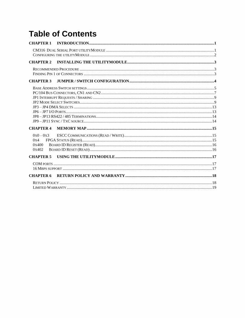
Table of Contents
CHAPTER 1 INTRODUCTION ............................................................................................................................ 1
CM316 DUAL SERIAL PORT UTILITYMODULE ........................................................................................................... 1 CONFIGURING THE UTILITYMODULE ........................................................................................................................... 2
CHAPTER 2 INSTALLING THE UTILITYMODULE ...................................................................................... 3
RECOMMENDED PROCEDURE ..................................................................................................................................... 3 FINDING PIN 1 OF CONNECTORS ................................................................................................................................. 3
CHAPTER 3 JUMPER / SWITCH CONFIGURATION .................................................................................... 4
BASE ADDRESS SWITCH SETTINGS .............................................................................................................................. 5 PC/104 BUS CONNECTORS, CN1 AND CN2 ................................................................................................................ 7 JP1 INTERRUPT REQUESTS / SHARING ........................................................................................................................ 9 JP2 MODE SELECT SWITCHES ..................................................................................................................................... 9 JP3 – JP4 DMA SELECTS ......................................................................................................................................... 13 JP6 – JP7 I/O PORTS................................................................................................................................................. 13 JP8 – JP13 RS422 / 485 TERMINATIONS................................................................................................................... 14 JP9 – JP11 SYNC / TXC SOURCE ............................................................................................................................... 14
CHAPTER 4 MEMORY MAP ............................................................................................................................ 15
0X0 – 0X3 ESCC COMMUNICATIONS (READ / WRITE) ....................................................................................... 15 0X4 FPGA STATUS (READ)................................................................................................................................. 15 0X400 BOARD ID REGISTER (READ) .................................................................................................................... 16 0X402 BOARD ID RESET (READ) ......................................................................................................................... 16
CHAPTER 5 USING THE UTILITYMODULE ................................................................................................ 17
COM PORTS ............................................................................................................................................................. 17 16 MBPS SUPPORT .................................................................................................................................................... 17
CHAPTER 6 RETURN POLICY AND WARRANTY ...................................................................................... 18
RETURN POLICY ....................................................................................................................................................... 18 LIMITED WARRANTY ................................................................................................................................................ 19
Table of Tables
TABLE 1 CONNECTOR /JUMPER DESCRIPTION TABLE ..................................................................................................... 4 TABLE 2 BASE ADDRESS TABLE FOR COM PORTS .......................................................................................................... 5 TABLE 3 PC/104 XT BUS CONNECTOR ........................................................................................................................ 7 TABLE 4 PC/104 AT BUS CONNECTOR .......................................................................................................................... 8 TABLE 5 IRQ JUMPERS ................................................................................................................................................... 9 TABLE 6 MODE JUMPERS ............................................................................................................................................... 9 TABLE 7 JUMPERS OPTIONS FOR PORT A CLOCK SOURCES ........................................................................................... 11 TABLE 8 JUMPERS OPTIONS FOR PORT B CLOCK SOURCES ........................................................................................... 12 TABLE 9 DMA JUMPERS .............................................................................................................................................. 13 TABLE 10 USER I/O PORTS A AND B ............................................................................................................................ 13 TABLE 11 TERMINATION JUMPERS ............................................................................................................................... 14 TABLE 12 SYNC / CLK JUMPERS ................................................................................................................................... 14 TABLE 13 CM316 MEMORY MAP ................................................................................................................................ 15
Table of Figures FIGURE 1 CONNECTOR LOCATIONS ................................................................................................................................. 4
CM316 Dual Serial utilityModule 1 RTD Embedded Technologies, Inc.
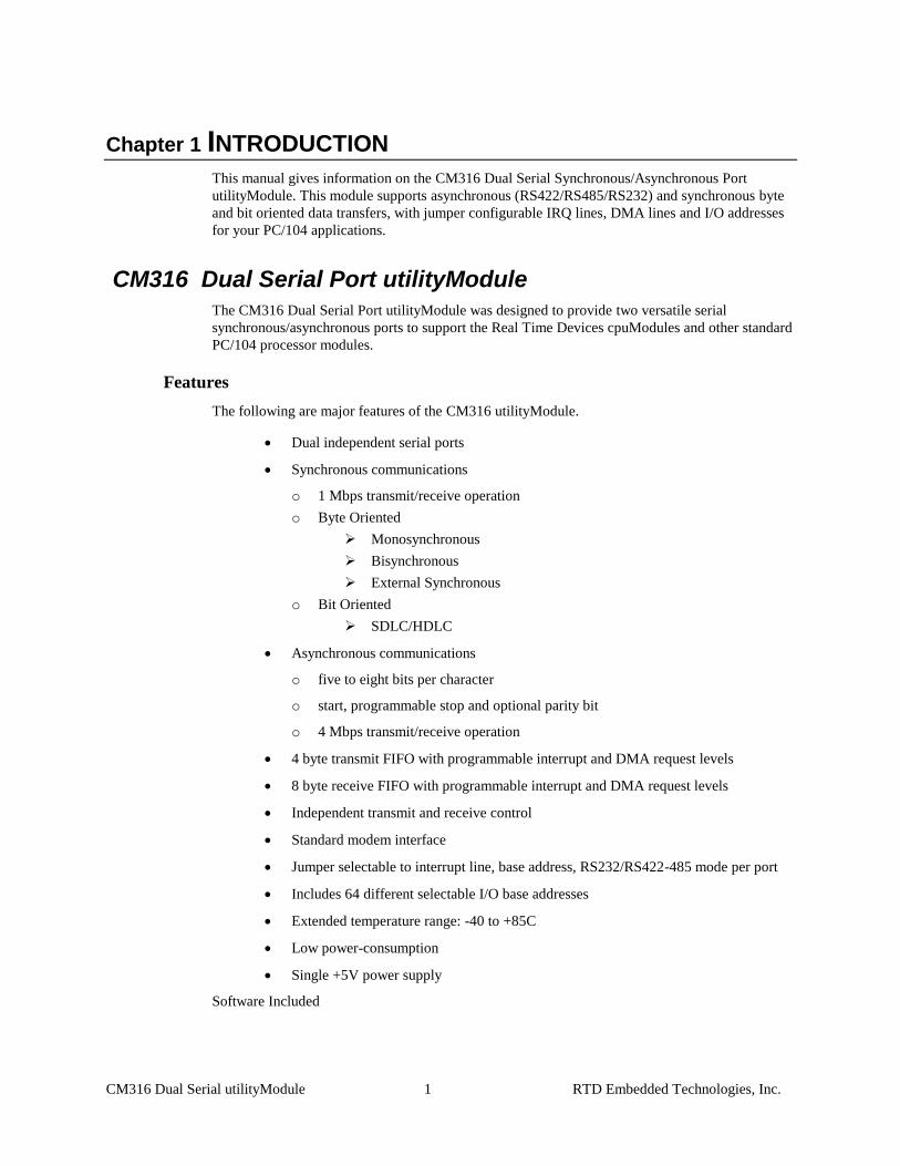
Chapter 1 INTRODUCTION This manual gives information on the CM316 Dual Serial Synchronous/Asynchronous Port
utilityModule. This module supports asynchronous (RS422/RS485/RS232) and synchronous byte
and bit oriented data transfers, with jumper configurable IRQ lines, DMA lines and I/O addresses
for your PC/104 applications.
CM316 Dual Serial Port utilityModule
The CM316 Dual Serial Port utilityModule was designed to provide two versatile serial
synchronous/asynchronous ports to support the Real Time Devices cpuModules and other standard
PC/104 processor modules.
Features
The following are major features of the CM316 utilityModule.
Dual independent serial ports
Synchronous communications
o 1 Mbps transmit/receive operation
o Byte Oriented
Monosynchronous
Bisynchronous
External Synchronous
o Bit Oriented
SDLC/HDLC
Asynchronous communications
o five to eight bits per character
o start, programmable stop and optional parity bit
o 4 Mbps transmit/receive operation
4 byte transmit FIFO with programmable interrupt and DMA request levels
8 byte receive FIFO with programmable interrupt and DMA request levels
Independent transmit and receive control
Standard modem interface
Jumper selectable to interrupt line, base address, RS232/RS422-485 mode per port
Includes 64 different selectable I/O base addresses
Extended temperature range: -40 to +85C
Low power-consumption
Single +5V power supply
Software Included
CM316 Dual Serial utilityModule 2 RTD Embedded Technologies, Inc.
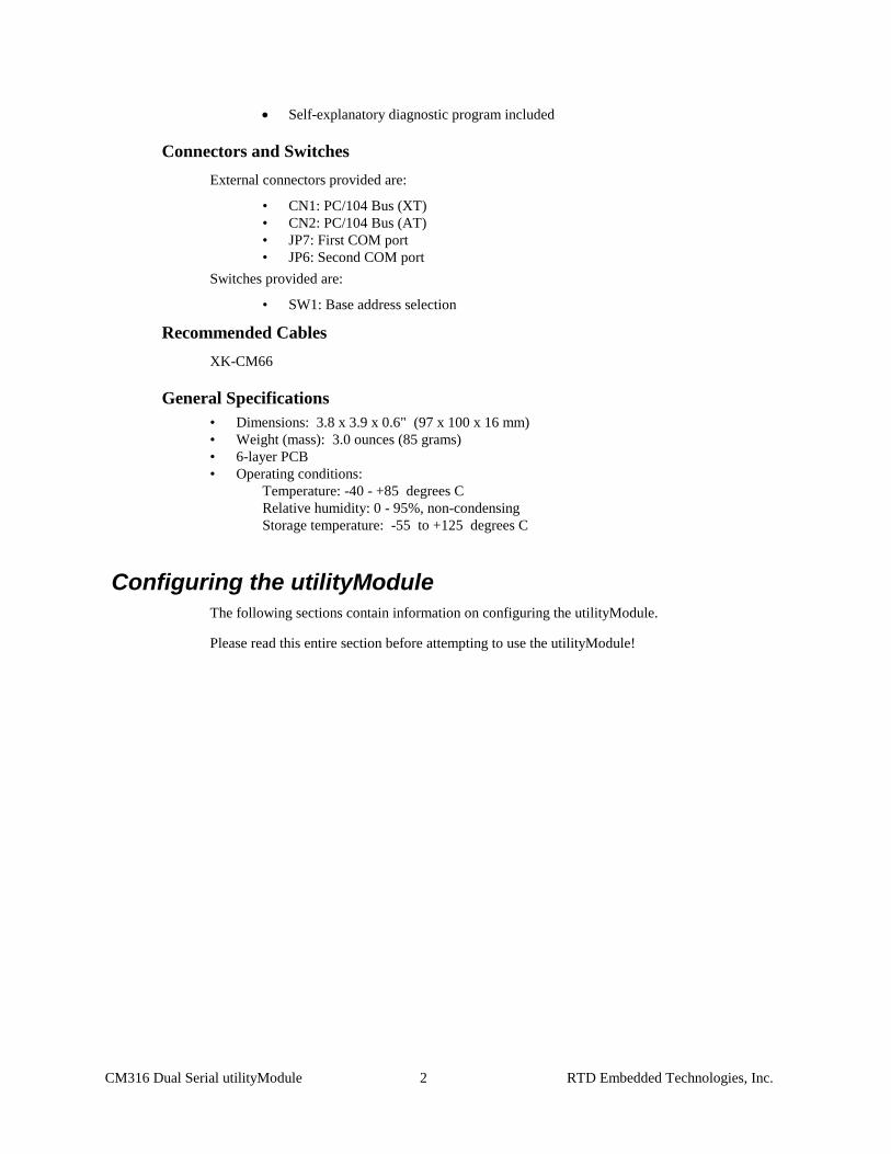
Self-explanatory diagnostic program included
Connectors and Switches
External connectors provided are:
• CN1: PC/104 Bus (XT)
• CN2: PC/104 Bus (AT)
• JP7: First COM port
• JP6: Second COM port
Switches provided are:
• SW1: Base address selection
Recommended Cables
XK-CM66
General Specifications
• Dimensions: 3.8 x 3.9 x 0.6" (97 x 100 x 16 mm)
• Weight (mass): 3.0 ounces (85 grams)
• 6-layer PCB
• Operating conditions:
Temperature: -40 - +85 degrees C
Relative humidity: 0 - 95%, non-condensing
Storage temperature: -55 to +125 degrees C
Configuring the utilityModule
The following sections contain information on configuring the utilityModule.
Please read this entire section before attempting to use the utilityModule!

CM316 Dual Serial utilityModule 3 RTD Embedded Technologies, Inc.
Chapter 2 INSTALLING THE UTILITYMODULE
Since the utilityModule uses a PC/104 stackthrough bus, the only hardware installation you will do
is placing the module to the PC/104 stack. To do this, you will connect the PC/104 bus connector
with the matching connector of another module.
Recommended Procedure
We recommend you follow the procedure below to ensure that stacking of the modules does not
damage connectors or electronics.
Turn off power to the PC/104 system or stack.
Select and install standoffs to properly position the utilityModule on the PC/104 stack.
Touch a grounded metal part of the stack to discharge any buildup of static electricity.
Remove the utilityModule from its anti-static bag.
Check that keying pins in the PC/104 bus connector are properly positioned.
Check the stacking order: make sure an XT bus card will not be placed between two AT bus
cards, or it will interrupt the AT bus signals.
Hold the utilityModule by its edges and orient it so the bus connector pins line up with the
matching connector on the stack.
Gently and evenly press the utilityModule onto the PC/104 stack.
CAUTION: Do not force the module onto the stack! Wiggling the module or applying too much
force may damage it. If the module does not readily press into place, remove it, check
for bent pins or out-of-place keying pins, and try again.
Connecting the utilityModule
The following sections describe connectors of the utilityModule.
Finding Pin 1 of Connectors
A white area silk-screened on the PC board indicates pin 1 of connectors. A square solder pad
visible on the bottom of the PC board also indicates it.
CM316 Dual Serial utilityModule 4 RTD Embedded Technologies, Inc.
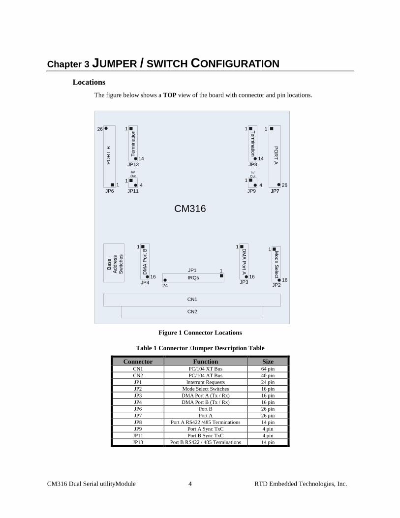
Chapter 3 JUMPER / SWITCH CONFIGURATION
Locations
The figure below shows a TOP view of the board with connector and pin locations.
CN2
CN1
Ba
se
Ad
dre
ss
Sw
itch
es
JP7
Te
rmin
atio
n
Te
rmin
atio
n
JP13 JP8
DM
A P
ort
B
JP4
DM
A P
ort A
JP3
Mo
de
Se
lect
JP2
IRQs
JP1
In/
OutIn/
Out
JP11 JP9
PO
RT
A1
JP7
26
PO
RT
B
1
JP6
26
1
16
1
24
1
16
1
16
14
1 1
1414
14
CM316
Figure 1 Connector Locations
Table 1 Connector /Jumper Description Table
Connector Function Size CN1 PC/104 XT Bus 64 pin
CN2 PC/104 AT Bus 40 pin
JP1 Interrupt Requests 24 pin
JP2 Mode Select Switches 16 pin
JP3 DMA Port A (Tx / Rx) 16 pin
JP4 DMA Port B (Tx / Rx) 16 pin
JP6 Port B 26 pin
JP7 Port A 26 pin
JP8 Port A RS422 /485 Terminations 14 pin
JP9 Port A Sync TxC 4 pin
JP11 Port B Sync TxC 4 pin
JP13 Port B RS422 / 485 Terminations 14 pin
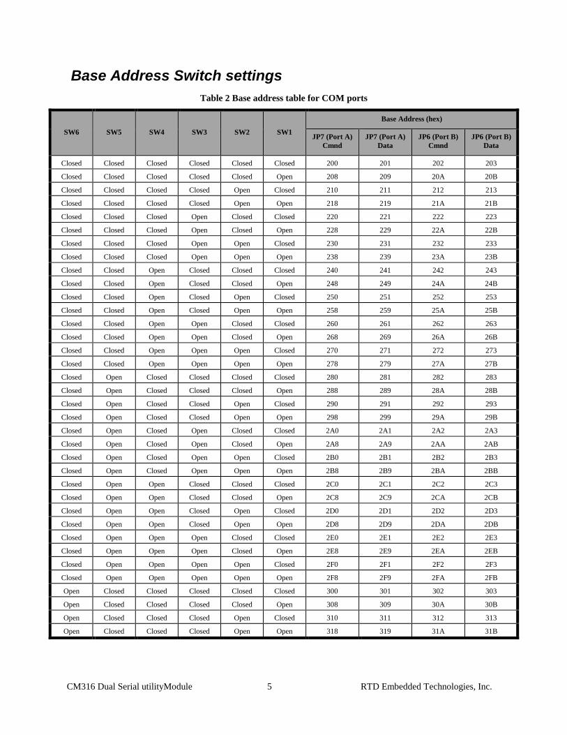
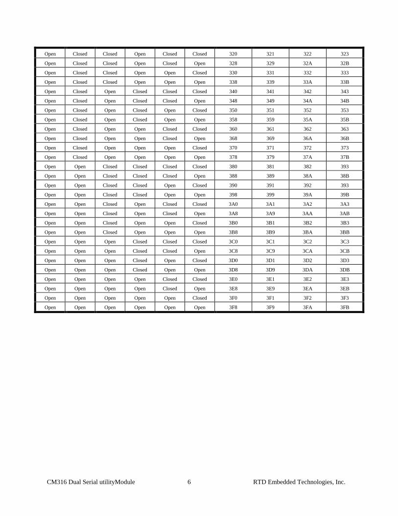
CM316 Dual Serial utilityModule 5 RTD Embedded Technologies, Inc.
Base Address Switch settings
Table 2 Base address table for COM ports
SW6 SW5 SW4 SW3 SW2 SW1
Base Address (hex)
JP7 (Port A)
Cmnd
JP7 (Port A)
Data
JP6 (Port B)
Cmnd
JP6 (Port B)
Data
Closed Closed Closed Closed Closed Closed 200 201 202 203
Closed Closed Closed Closed Closed Open 208 209 20A 20B
Closed Closed Closed Closed Open Closed 210 211 212 213
Closed Closed Closed Closed Open Open 218 219 21A 21B
Closed Closed Closed Open Closed Closed 220 221 222 223
Closed Closed Closed Open Closed Open 228 229 22A 22B
Closed Closed Closed Open Open Closed 230 231 232 233
Closed Closed Closed Open Open Open 238 239 23A 23B
Closed Closed Open Closed Closed Closed 240 241 242 243
Closed Closed Open Closed Closed Open 248 249 24A 24B
Closed Closed Open Closed Open Closed 250 251 252 253
Closed Closed Open Closed Open Open 258 259 25A 25B
Closed Closed Open Open Closed Closed 260 261 262 263
Closed Closed Open Open Closed Open 268 269 26A 26B
Closed Closed Open Open Open Closed 270 271 272 273
Closed Closed Open Open Open Open 278 279 27A 27B
Closed Open Closed Closed Closed Closed 280 281 282 283
Closed Open Closed Closed Closed Open 288 289 28A 28B
Closed Open Closed Closed Open Closed 290 291 292 293
Closed Open Closed Closed Open Open 298 299 29A 29B
Closed Open Closed Open Closed Closed 2A0 2A1 2A2 2A3
Closed Open Closed Open Closed Open 2A8 2A9 2AA 2AB
Closed Open Closed Open Open Closed 2B0 2B1 2B2 2B3
Closed Open Closed Open Open Open 2B8 2B9 2BA 2BB
Closed Open Open Closed Closed Closed 2C0 2C1 2C2 2C3
Closed Open Open Closed Closed Open 2C8 2C9 2CA 2CB
Closed Open Open Closed Open Closed 2D0 2D1 2D2 2D3
Closed Open Open Closed Open Open 2D8 2D9 2DA 2DB
Closed Open Open Open Closed Closed 2E0 2E1 2E2 2E3
Closed Open Open Open Closed Open 2E8 2E9 2EA 2EB
Closed Open Open Open Open Closed 2F0 2F1 2F2 2F3
Closed Open Open Open Open Open 2F8 2F9 2FA 2FB
Open Closed Closed Closed Closed Closed 300 301 302 303
Open Closed Closed Closed Closed Open 308 309 30A 30B
Open Closed Closed Closed Open Closed 310 311 312 313
Open Closed Closed Closed Open Open 318 319 31A 31B
CM316 Dual Serial utilityModule 6 RTD Embedded Technologies, Inc.
Open Closed Closed Open Closed Closed 320 321 322 323
Open Closed Closed Open Closed Open 328 329 32A 32B
Open Closed Closed Open Open Closed 330 331 332 333
Open Closed Closed Open Open Open 338 339 33A 33B
Open Closed Open Closed Closed Closed 340 341 342 343
Open Closed Open Closed Closed Open 348 349 34A 34B
Open Closed Open Closed Open Closed 350 351 352 353
Open Closed Open Closed Open Open 358 359 35A 35B
Open Closed Open Open Closed Closed 360 361 362 363
Open Closed Open Open Closed Open 368 369 36A 36B
Open Closed Open Open Open Closed 370 371 372 373
Open Closed Open Open Open Open 378 379 37A 37B
Open Open Closed Closed Closed Closed 380 381 382 393
Open Open Closed Closed Closed Open 388 389 38A 38B
Open Open Closed Closed Open Closed 390 391 392 393
Open Open Closed Closed Open Open 398 399 39A 39B
Open Open Closed Open Closed Closed 3A0 3A1 3A2 3A3
Open Open Closed Open Closed Open 3A8 3A9 3AA 3AB
Open Open Closed Open Open Closed 3B0 3B1 3B2 3B3
Open Open Closed Open Open Open 3B8 3B9 3BA 3BB
Open Open Open Closed Closed Closed 3C0 3C1 3C2 3C3
Open Open Open Closed Closed Open 3C8 3C9 3CA 3CB
Open Open Open Closed Open Closed 3D0 3D1 3D2 3D3
Open Open Open Closed Open Open 3D8 3D9 3DA 3DB
Open Open Open Open Closed Closed 3E0 3E1 3E2 3E3
Open Open Open Open Closed Open 3E8 3E9 3EA 3EB
Open Open Open Open Open Closed 3F0 3F1 3F2 3F3
Open Open Open Open Open Open 3F8 3F9 3FA 3FB

CM316 Dual Serial utilityModule 7 RTD Embedded Technologies, Inc.
PC/104 Bus Connectors, CN1 and CN2
Connectors CN1 and CN2 provide PC/104 bus connections. CN1 carries XT bus signals, and CN2
carries additional signals for the AT bus. The signals on CN1 and CN2 conform to the IEEE P966
standard for the PC/104 bus.
The following tables list the connector pinouts:
Table 3 PC/104 XT Bus Connector
PC/104 XT Bus Connector, CN1
Pin Row A Row B 1 IOCHCHK* 0V
2 SD7 RESETDRV
3 SD6 +5V
4 SD5 IRQ9
5 SD4 -5V
6 SD3 DRQ2
7 SD2 -12V
8 SD1 ENDXFR*
9 SD0 +12V
10 IOCHRDY (KEYING PIN)
11 AEN SMEMW*
12 SA19 SMEMR*
13 SA18 IOW*
14 SA17 IOR*
15 SA16 DACK3
16 SA15 DRQ3
17 SA14 DACK1*
18 SA13 DRQ1
19 SA12 REFRESH
20 SA11 SYSCLK
21 SA10 IRQ7
22 SA9 IRQ6
23 SA8 IRQ5
24 SA7 IRQ4
25 SA6 IRQ3
26 SA5 DACK2*
27 SA4 TC
28 SA3 BALE
29 SA2 +5V
30 SA1 OSC
31 SA0 0V
32 0V 0V

CM316 Dual Serial utilityModule 8 RTD Embedded Technologies, Inc.
Table 4 PC/104 AT Bus Connector
PC/104 AT Bus Connector, CN2
Pin Row C Row D 0 0V 0V
1 SBHE* MEMCS16*
2 LA23 IOCS16*
3 LA22 IRQ10
4 LA21 IRQ11
5 LA20 IRQ12
6 LA19 IRQ15
7 LA18 IRQ14
8 LA17 DACK0*
9 MEMR* DRQ0
10 MEMW* DACK5*
11 SD8 DRQ5
12 SD9 DACK6*
13 SD10 DRQ6
14 SD11 DRQ6
15 SD12 DRQ7
16 SD13 +5V
17 SD14 MASTER*
18 SD15 0V
19 (KEYING PIN) 0V
Note: Two locations on the bus have mechanical keying pins to help prevent misconnection
of the PC/104 bus. These keying pins are a part of the PC/104 standard, and we
strongly recommend you leave them in place.
If you have other modules without keying pins, we suggest you modify them to
include keying.

CM316 Dual Serial utilityModule 9 RTD Embedded Technologies, Inc.
JP1 Interrupt Requests / Sharing Interrupt sharing is a mechanism which allows different devices or different boards to share the
same active high IRQ lines on the PC/104 bus, given that there is a interrupt sharing circuit
associated with each device / board. The utilityModule provides interrupt-sharing circuits for the
board; thus allowing sharing of each IRQ line with other boards.
Interrupt sharing in a PC/104 system requires one 1K pull-down resistor per IRQ line for all the
devices that share the IRQ. Installing a ground jumper in the utilityModule will pull its associated
IRQ line down with 1K resistor. When multiple boards are placed in a system care should be
taken not to install the ground jumper on more than one board as this will reduce the pull down
resistor value increasing the effective drive load, which in turn will keep devices from driving the
IRQ line high. With one board installed in the system JP1 (23-24) must be jumpered since the
driver is an open emitter type. For more than one board or for multiple IRQ sharing boards
only one ground jumper needs to be installed for the system.
Table 5 IRQ Jumpers
Description Jumper Pins IRQ 3 1-2
IRQ 4 3-4
IRQ 5 5-6
IRQ 6 7-8
IRQ 7 9-10
IRQ 9 11-12
IRQ 10 13-14
IRQ 11 15-16
IRQ 12 17-18
IRQ 14 19-20
IRQ 15 21-22
GND 23-24
JP2 Mode Select Switches
Table 6 Mode Jumpers
Description Pins Open Shorted Port A Serial Comm Mode 1-2 RS422 / 485 RS232
Port A Int / Ext Sync / TxClk 3-4 External Internal
Port A Request To Send / Always 5-6 Always RTS
14.7456MHz / 16.0000MHz 7-8 16MHz 14MHz
Port B Serial Comm Mode 9-10 RS422 / 485 RS232
Port B Int / Ext Sync / TxClk 11-12 External Internal
Port B Request To Send / Always 13-14 Always RTS
ESCC ZiLOG Rx Clock Source 15-16 Rx Clk Tx Clk
Port x Serial Comm Mode
Makes appropriate port A or B either differential mode (RS422/485) or single ended mode
(RS232).

CM316 Dual Serial utilityModule 10 RTD Embedded Technologies, Inc.
Port x Int / Ext Sync and ESCC Transmit Clock
WARNING WHEN SYNC OR TRANSMIT CLOCK SOURCE IS FROM THE EXTERNAL
CONNECTOR (JP7 FOR PORT A, JP6 FOR PORT B) THE APPROPRIATE PIN ON THE ESCC
SHOULD BE MADE AS AN INPUT TO AVOID DRIVER CONTENTION AND POSSIBLE DAMAGE TO THE
BOARD.
When left open the clock and sync source come from the appropriate connector (JP7 for Port A,
JP6 for Port B). When shorted the ESCC is the source for the transmitter clock and sync signal
and the appropriate pins at JP7 and JP6 become outputs.
Port x Request to Send /Always
The RS422/485 on board drivers have two physical enables and this jumper is used to enable one
of these enables either always or with the request to send signal.
14.7456MHz / 16.0000MHz
This jumper is the clock source for the ESCC ZiLOG chip.
ESCC ZiLOG Rx Clock Source
This jumper determines whether the receive clock source for the ESCC is the transmitter clock
(this may be onboard or external) or the receiver clock from the connector. See the table below for
the list of options. Care should be taken to NOT have an external driver on the connector in
certain instances (see below table).

CM316 Dual Serial utilityModule 11 RTD Embedded Technologies, Inc.
RS232
RS422
Table 7 Jumpers Options for Port A clock sources
JP2 JP9
Description
Pins 15-16 Pins 1-2 Pins 3-4 Pins 3-4
RX CLK
source
RS 422 /232 TX CLK
source
To output
connector
ESCC Rx source ESCC Tx Source Tx Conn Source
Closed Closed Open Closed Rx 232 Ext
Rx 232 Ext
Rx 232 Ext
Closed Closed Open Open Tx 232 Ext None
Closed Closed Closed Closed Tx Loopback
None
Tx 232 USART
Closed Closed Closed Open Tx 232 Ext None
Open Closed Closed Closed
Rx 232 Ext
Tx 232 USART
Open Closed Closed Open None
Open Closed Open Closed
Rx 232 Ext
Rx 232 Ext
Open Closed Open Open None
Closed Open Closed Closed Tx Loopback
None
Tx 422 USART
Closed Open Closed Open None Partially driven Tx
422 USART
Open Open Closed Closed
Rx 422 Ext
Tx 422 USART
Open Open Closed Open Partially driven Tx
422 USART
Open Open Open Closed
Rx 422 Ext None
Open Open Open Open
Closed Open Open Closed
Tx 422 Ext
Closed Open Open Open
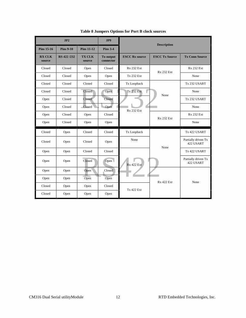
CM316 Dual Serial utilityModule 12 RTD Embedded Technologies, Inc.
RS232
RS422
Table 8 Jumpers Options for Port B clock sources
JP2 JP9
Description
Pins 15-16 Pins 9-10 Pins 11-12 Pins 3-4
RX CLK
source
RS 422 /232 TX CLK
source
To output
connector
ESCC Rx source ESCC Tx Source Tx Conn Source
Closed Closed Open Closed Rx 232 Ext
Rx 232 Ext
Rx 232 Ext
Closed Closed Open Open Tx 232 Ext None
Closed Closed Closed Closed Tx Loopback
None
Tx 232 USART
Closed Closed Closed Open Tx 232 Ext None
Open Closed Closed Closed
Rx 232 Ext
Tx 232 USART
Open Closed Closed Open None
Open Closed Open Closed
Rx 232 Ext
Rx 232 Ext
Open Closed Open Open None
Closed Open Closed Closed Tx Loopback
None
Tx 422 USART
Closed Open Closed Open None Partially driven Tx
422 USART
Open Open Closed Closed
Rx 422 Ext
Tx 422 USART
Open Open Closed Open Partially driven Tx
422 USART
Open Open Open Closed
Rx 422 Ext None
Open Open Open Open
Closed Open Open Closed
Tx 422 Ext
Closed Open Open Open
CM316 Dual Serial utilityModule 13 RTD Embedded Technologies, Inc.
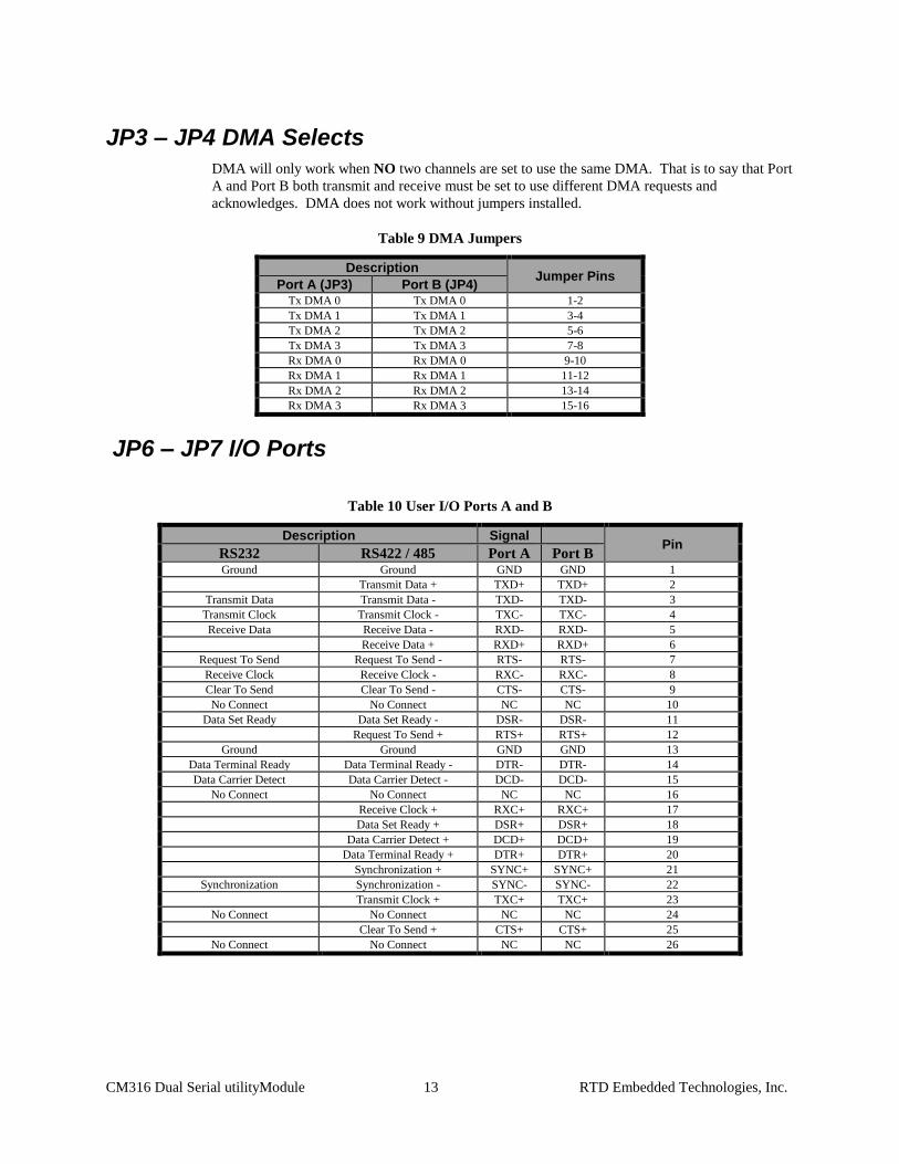
JP3 – JP4 DMA Selects
DMA will only work when NO two channels are set to use the same DMA. That is to say that Port
A and Port B both transmit and receive must be set to use different DMA requests and
acknowledges. DMA does not work without jumpers installed.
Table 9 DMA Jumpers
Description Jumper Pins
Port A (JP3) Port B (JP4) Tx DMA 0 Tx DMA 0 1-2
Tx DMA 1 Tx DMA 1 3-4
Tx DMA 2 Tx DMA 2 5-6
Tx DMA 3 Tx DMA 3 7-8
Rx DMA 0 Rx DMA 0 9-10
Rx DMA 1 Rx DMA 1 11-12
Rx DMA 2 Rx DMA 2 13-14
Rx DMA 3 Rx DMA 3 15-16
JP6 – JP7 I/O Ports
Table 10 User I/O Ports A and B
Description Signal Pin
RS232 RS422 / 485 Port A Port B Ground Ground GND GND 1
Transmit Data + TXD+ TXD+ 2
Transmit Data Transmit Data - TXD- TXD- 3
Transmit Clock Transmit Clock - TXC- TXC- 4
Receive Data Receive Data - RXD- RXD- 5
Receive Data + RXD+ RXD+ 6
Request To Send Request To Send - RTS- RTS- 7
Receive Clock Receive Clock - RXC- RXC- 8
Clear To Send Clear To Send - CTS- CTS- 9
No Connect No Connect NC NC 10
Data Set Ready Data Set Ready - DSR- DSR- 11
Request To Send + RTS+ RTS+ 12
Ground Ground GND GND 13
Data Terminal Ready Data Terminal Ready - DTR- DTR- 14
Data Carrier Detect Data Carrier Detect - DCD- DCD- 15
No Connect No Connect NC NC 16
Receive Clock + RXC+ RXC+ 17
Data Set Ready + DSR+ DSR+ 18
Data Carrier Detect + DCD+ DCD+ 19
Data Terminal Ready + DTR+ DTR+ 20
Synchronization + SYNC+ SYNC+ 21
Synchronization Synchronization - SYNC- SYNC- 22
Transmit Clock + TXC+ TXC+ 23
No Connect No Connect NC NC 24
Clear To Send + CTS+ CTS+ 25
No Connect No Connect NC NC 26
CM316 Dual Serial utilityModule 14 RTD Embedded Technologies, Inc.
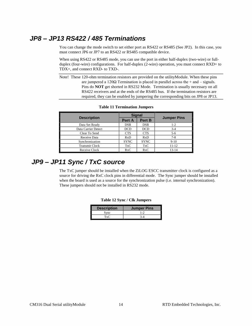
JP8 – JP13 RS422 / 485 Terminations
You can change the mode switch to set either port as RS422 or RS485 (See JP2). In this case, you
must connect JP6 or JP7 to an RS422 or RS485 compatible device.
When using RS422 or RS485 mode, you can use the port in either half-duplex (two-wire) or full-
duplex (four-wire) configurations. For half-duplex (2-wire) operation, you must connect RXD+ to
TDX+, and connect RXD- to TXD-.
Note! These 120-ohm termination resistors are provided on the utilityModule. When these pins
are jumpered a 120Ω Termination is placed in parallel across the + and – signals.
Pins do NOT get shorted in RS232 Mode. Termination is usually necessary on all
RS422 receivers and at the ends of the RS485 bus. If the termination resistors are
required, they can be enabled by jumpering the corresponding bits on JP8 or JP13.
Table 11 Termination Jumpers
Description Signal
Jumper Pins Port A Port B
Data Set Ready DSR DSR 1-2
Data Carrier Detect DCD DCD 3-4
Clear To Send CTS CTS 5-6
Receive Data RxD RxD 7-8
Synchronization SYNC SYNC 9-10
Transmit Clock TxC TxC 11-12
Receive Clock RxC RxC 13-14
JP9 – JP11 Sync / TxC source
The TxC jumper should be installed when the ZiLOG ESCC transmitter clock is configured as a
source for driving the RxC clock pins in differential mode. The Sync jumper should be installed
when the board is used as a source for the synchronization pulse (i.e. internal synchronization).
These jumpers should not be installed in RS232 mode.
Table 12 Sync / Clk Jumpers
Description Jumper Pins Sync 1-2
TxC 3-4
CM316 Dual Serial utilityModule 15 RTD Embedded Technologies, Inc.
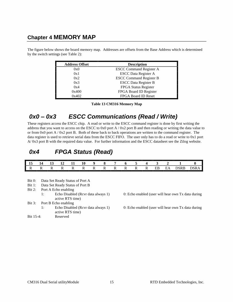
Chapter 4 MEMORY MAP
The figure below shows the board memory map. Addresses are offsets from the Base Address which is determined
by the switch settings (see Table 2):
Address Offset Description
0x0 ESCC Command Register A
0x1 ESCC Data Register A
0x2 ESCC Command Register B
0x3 ESCC Data Register B
0x4 FPGA Status Register
0x400 FPGA Board ID Register
0x402 FPGA Board ID Reset
Table 13 CM316 Memory Map
0x0 – 0x3 ESCC Communications (Read / Write) These registers access the ESCC chip. A read or write to the ESCC command register is done by first writing the
address that you want to access on the ESCC to 0x0 port A / 0x2 port B and then reading or writing the data value to
or from 0x0 port A / 0x2 port B. Both of these back to back operations are written to the command register. The
data register is used to retrieve serial data from the ESCC FIFO. The user only has to do a read or write to 0x1 port
A/ 0x3 port B with the required data value. For further information and the ESCC datasheet see the Zilog website.
0x4 FPGA Status (Read)
15 14 13 12 11 10 9 8 7 6 5 4 3 2 1 0
R R R R R R R R R R R R EB EA DSRB DSRA
Bit 0: Data Set Ready Status of Port A
Bit 1: Data Set Ready Status of Port B
Bit 2: Port A Echo enabling
1: Echo Disabled (Rcvr data always 1) 0: Echo enabled (user will hear own Tx data during
active RTS time)
Bit 3: Port B Echo enabling
1: Echo Disabled (Rcvr data always 1) 0: Echo enabled (user will hear own Tx data during
active RTS time)
Bit 15-4: Reserved
CM316 Dual Serial utilityModule 16 RTD Embedded Technologies, Inc.
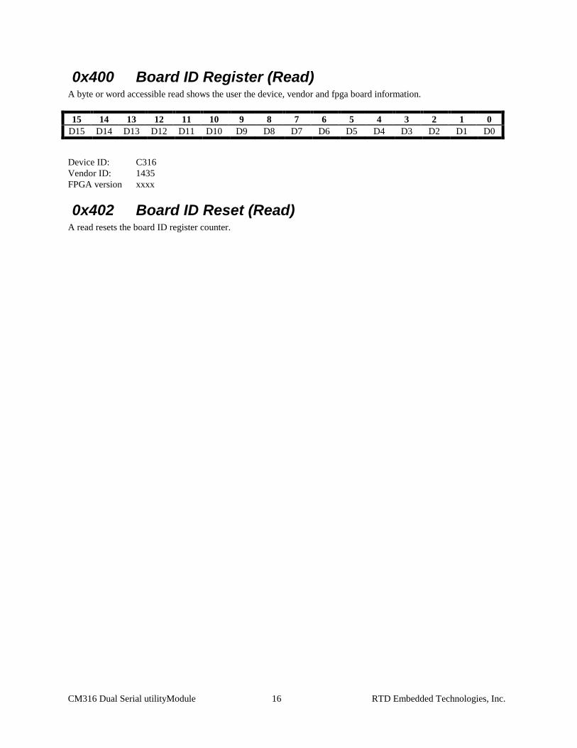
0x400 Board ID Register (Read) A byte or word accessible read shows the user the device, vendor and fpga board information.
15 14 13 12 11 10 9 8 7 6 5 4 3 2 1 0
D15 D14 D13 D12 D11 D10 D9 D8 D7 D6 D5 D4 D3 D2 D1 D0
Device ID: C316
Vendor ID: 1435
FPGA version xxxx
0x402 Board ID Reset (Read) A read resets the board ID register counter.
CM316 Dual Serial utilityModule 17 RTD Embedded Technologies, Inc.
Chapter 5 USING THE UTILITYMODULE
COM ports
The utilityModule features Zilog dual Enhanced Synchronous Communications Controller (ESCC)
Z85230 part.
ZiLOG Documentation
Due to the complexity of the Zilog serial chip, it is impossible for us to reproduce all programming
information in this manual. If you will be doing in-depth programming of the serial port controller,
we suggest you obtain the Z85230 datasheet / apnotes from the manufacturer.
The Z85230 datasheet is available on-line in electronic format as an Adobe Acrobat (. PDF) file on
the Zilog website:
www.zilog.com
You may also contact:
Zilog Worldwide Headquarters
532 Race Street
San Jose, CA 95126-3432
Or by phone/fax:
Phone: 408-558-8500
Fax: 408-558-8300
16 Mbps support
With 16 MHz clock input selected (JP2, 7-8 left open), the utilityModule is capable of provide
data rates up to 16 Mbps using NRZ encoding in RS422/RS485 mode. Since RS232 standard
restricts data rate to 20 Kbps, you might experience failure at higher data rate above 250 Kbps
with 16 MHz clock select for the utilityModule.
CM316 Dual Serial utilityModule 18 RTD Embedded Technologies, Inc.
Chapter 6 RETURN POLICY AND WARRANTY
Return Policy
If you wish to return a product to the factory for service, please follow this procedure:
Read the Limited Warranty to familiarize yourself with our warranty policy.
Contact the factory for a Return Merchandise Authorization (RMA) number.
Please have the following available:
• Complete board name
• Board serial number
• A detailed description of the board’s behavior
List the name of a contact person, familiar with technical details of the problem or situation, along
with their phone and fax numbers, address, and e-mail address (if available).
List your shipping address!!
Indicate the shipping method you would like used to return the product to you.
We will not ship by next-day service without your pre-approval.
Carefully package the product, using proper anti-static packaging.
Write the RMA number in large (1") letters on the outside of the package.
Return the package to:
RTD Embedded Technologies, Inc.
103 Innovation Blvd.
State College PA 16803-0906
USA

CM316 Dual Serial utilityModule 19 RTD Embedded Technologies, Inc.
Limited Warranty
RTD Embedded Technologies, Inc. warrants the hardware and software products it manufactures and
produces to be free from defects in materials and workmanship for one year following the date of shipment
from RTD Embedded Technologies, INC. This warranty is limited to the original purchaser of product and
is not transferable.
During the one year warranty period, RTD Embedded Technologies will repair or replace, at its option, any
defective products or parts at no additional charge, provided that the product is returned, shipping prepaid,
to RTD Embedded Technologies. All replaced parts and products become the property of RTD Embedded
Technologies. Before returning any product for repair, customers are required to contact the factory for an
RMA number.
THIS LIMITED WARRANTY DOES NOT EXTEND TO ANY PRODUCTS WHICH HAVE BEEN
DAMAGED AS A RESULT OF ACCIDENT, MISUSE, ABUSE (such as: use of incorrect input voltages,
improper or insufficient ventilation, failure to follow the operating instructions that are provided by RTD
Embedded Technologies, "acts of God" or other contingencies beyond the control of RTD Embedded
Technologies), OR AS A RESULT OF SERVICE OR MODIFICATION BY ANYONE OTHER THAN
RTD Embedded Technologies. EXCEPT AS EXPRESSLY SET FORTH ABOVE, NO OTHER
WARRANTIES ARE EXPRESSED OR IMPLIED, INCLUDING, BUT NOT LIMITED TO, ANY
IMPLIED WARRANTIES OF MERCHANTABILITY AND FITNESS FOR A PARTICULAR
PURPOSE, AND RTD Embedded Technologies EXPRESSLY DISCLAIMS ALL WARRANTIES NOT
STATED HEREIN. ALL IMPLIED WARRANTIES, INCLUDING IMPLIED WARRANTIES FOR
MECHANTABILITY AND FITNESS FOR A PARTICULAR PURPOSE, ARE LIMITED TO THE
DURATION OF THIS WARRANTY. IN THE EVENT THE PRODUCT IS NOT FREE FROM
DEFECTS AS WARRANTED ABOVE, THE PURCHASER'S SOLE REMEDY SHALL BE REPAIR OR
REPLACEMENT AS PROVIDED ABOVE. UNDER NO CIRCUMSTANCES WILL RTD Embedded
Technologies BE LIABLE TO THE PURCHASER OR ANY USER FOR ANY DAMAGES,
INCLUDING ANY INCIDENTAL OR CONSEQUENTIAL DAMAGES, EXPENSES, LOST PROFITS,
LOST SAVINGS, OR OTHER DAMAGES ARISING OUT OF THE USE OR INABILITY TO USE THE
PRODUCT.
SOME STATES DO NOT ALLOW THE EXCLUSION OR LIMITATION OF INCIDENTAL OR
CONSEQUENTIAL DAMAGES FOR CONSUMER PRODUCTS, AND SOME STATES DO NOT
ALLOW LIMITATIONS ON HOW LONG AN IMPLIED WARRANTY LASTS, SO THE ABOVE
LIMITATIONS OR EXCLUSIONS MAY NOT APPLY TO YOU.
THIS WARRANTY GIVES YOU SPECIFIC LEGAL RIGHTS, AND YOU MAY ALSO HAVE OTHER
RIGHTS WHICH VARY FROM STATE TO STATE.

CM316 Dual Serial utilityModule 20 RTD Embedded Technologies, Inc.
RTD Embedded Technologies, Inc.
103 Innovation Blvd.
State College PA 16803-0906
USA
Our website: www.rtd.com