Embed Size (px)
Citation preview
1/13 www.rohm.com 2012.01 - Rev.C© 2012 ROHM Co., Ltd. All rights reserved.
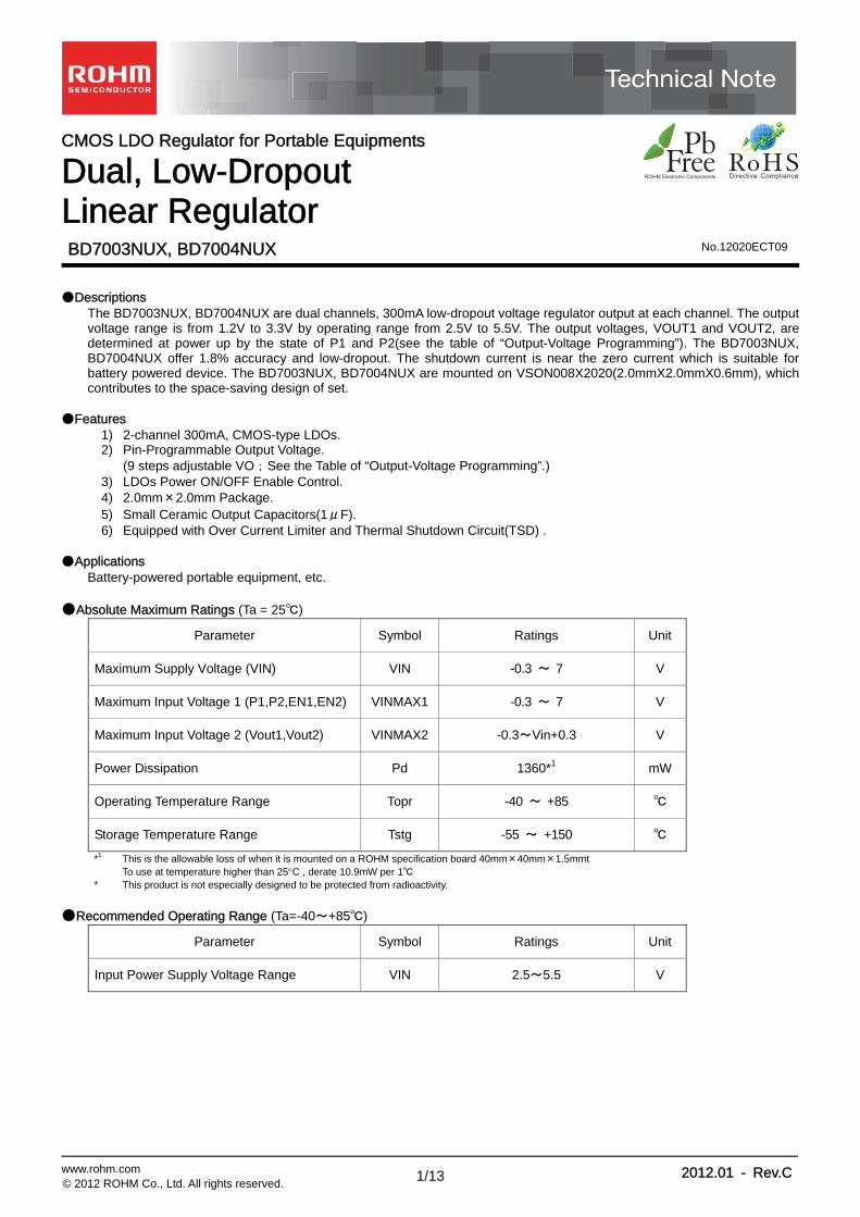
CMOS LDO Regulator for Portable Equipments
Dual, Low-Dropout Linear Regulator BD7003NUX, BD7004NUX
●Descriptions
The BD7003NUX, BD7004NUX are dual channels, 300mA low-dropout voltage regulator output at each channel. The output voltage range is from 1.2V to 3.3V by operating range from 2.5V to 5.5V. The output voltages, VOUT1 and VOUT2, are determined at power up by the state of P1 and P2(see the table of “Output-Voltage Programming”). The BD7003NUX, BD7004NUX offer 1.8% accuracy and low-dropout. The shutdown current is near the zero current which is suitable for battery powered device. The BD7003NUX, BD7004NUX are mounted on VSON008X2020(2.0mmX2.0mmX0.6mm), which contributes to the space-saving design of set.
●Features 1) 2-channel 300mA, CMOS-type LDOs. 2) Pin-Programmable Output Voltage. (9 steps adjustable VO;See the Table of “Output-Voltage Programming”.) 3) LDOs Power ON/OFF Enable Control. 4) 2.0mm×2.0mm Package. 5) Small Ceramic Output Capacitors(1μF). 6) Equipped with Over Current Limiter and Thermal Shutdown Circuit(TSD) .
●Applications
Battery-powered portable equipment, etc.
●Absolute Maximum Ratings (Ta = 25℃)
Parameter Symbol Ratings Unit
Maximum Supply Voltage (VIN) VIN -0.3 ~ 7 V
Maximum Input Voltage 1 (P1,P2,EN1,EN2) VINMAX1 -0.3 ~ 7 V
Maximum Input Voltage 2 (Vout1,Vout2) VINMAX2 -0.3~Vin+0.3 V
Power Dissipation Pd 1360*1 mW
Operating Temperature Range Topr -40 ~ +85 ℃
Storage Temperature Range Tstg -55 ~ +150 ℃
*1 This is the allowable loss of when it is mounted on a ROHM specification board 40mm×40mm×1.5mmt To use at temperature higher than 25C , derate 10.9mW per 1℃ * This product is not especially designed to be protected from radioactivity.
●Recommended Operating Range (Ta=-40~+85℃)
Parameter Symbol Ratings Unit
Input Power Supply Voltage Range VIN 2.5~5.5 V
No.12020ECT09
Technical Note
2/13 www.rohm.com 2012.01 - Rev.C© 2012 ROHM Co., Ltd. All rights reserved.
BD7003NUX,BD7004NUX
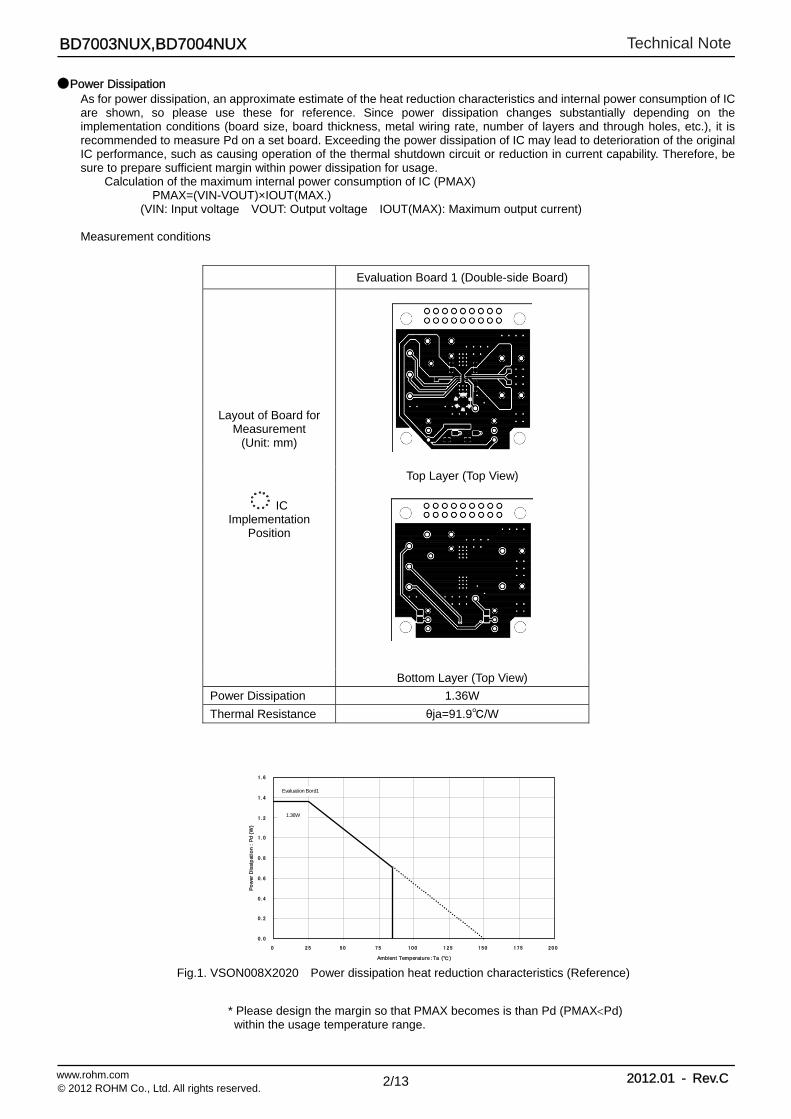
●Power Dissipation As for power dissipation, an approximate estimate of the heat reduction characteristics and internal power consumption of IC are shown, so please use these for reference. Since power dissipation changes substantially depending on the implementation conditions (board size, board thickness, metal wiring rate, number of layers and through holes, etc.), it is recommended to measure Pd on a set board. Exceeding the power dissipation of IC may lead to deterioration of the original IC performance, such as causing operation of the thermal shutdown circuit or reduction in current capability. Therefore, be sure to prepare sufficient margin within power dissipation for usage. Calculation of the maximum internal power consumption of IC (PMAX) PMAX=(VIN-VOUT)×IOUT(MAX.)
(VIN: Input voltage VOUT: Output voltage IOUT(MAX): Maximum output current)
Measurement conditions
Evaluation Board 1 (Double-side Board)
Layout of Board for Measurement
(Unit: mm)
IC Implementation
Position
Top Layer (Top View)
Bottom Layer (Top View)
Power Dissipation 1.36W
Thermal Resistance θja=91.9℃/W
Fig.1. VSON008X2020 Power dissipation heat reduction characteristics (Reference)
0 . 0
0 . 2
0 . 4
0 . 6
0 . 8
1 . 0
1 . 2
1 . 4
1 . 6
0 25 50 75 100 125 150 175 200
Ambient Temperature :Ta (℃ )
Po
wer
Dis
sip
atio
n :
Pd
(W
)
Evaluation Bord1
1.36W
* Please design the margin so that PMAX becomes is than Pd (PMAXPd) within the usage temperature range.

Technical Note
3/13 www.rohm.com 2012.01 - Rev.C© 2012 ROHM Co., Ltd. All rights reserved.
BD7003NUX,BD7004NUX
●Electrical Characteristics (Vin=3.7V, EN1=EN2=Vin,Ta =+25℃, unless otherwise noted.)
Parameter Symbol Limits
Unit Condition Min Typ Max
Output Voltage range VOUT 1.2 - 3.3 V
Input Voltage range VIN 2.5 - 5.5 V
Output Voltage Accuracy Δvouta -1.8 - 1.8 % Iout=1mA, VOUT≧1.5V
Δvoutb -30 - +30 mV Iout=1mA, VOUT=1.2V
Maximum Output Current Imax 300 - - mA
Short Circuit Current Isc - 150 - mA VOUT = 0V
Ground Pin Current Iq - 55 95
μA Iout=0mA
- 35 65 One LDO shutdown, Iout=0mA
Dropout Voltage Vdrop
- 120 170
mV
VIN=2.5V, VOUT=2.6V, Iout=100mA
- 90 140 VIN=2.7V, VOUT=2.8V, Iout=100mA
80 130 VIN=2.9V, VOUT=3.0V, Iout=100mA
- 70 120 VIN=3.2V, VOUT=3.3V,Iout=100mA
- 360 510 VIN=2.5V, VOUT=2.6V, Iout=300mA
- 270 420 VIN=2.7V, VOUT=2.8V, Iout=300mA
240 390 VIN=2.9V, VOUT=3.0V, Iout=300mA
- 210 360 VIN=3.2V, VOUT=3.3V, Iout=300mA
Line Regulation ΔVLNR - 0.02 0.2 %/V VIN=VOUT+1V to VIN=5.5V, Iout=10mA
Load Regulation ΔVLDR - 0.2 0.6 % Iout=1mA to 300mA
Ripple Rejection PSRR - 66 - dB f=100Hz,Iout=10mA@VOUT=1.5V
Output Noise en - 150 - μVrms fBW=10Hz to 100kHz;Iout=10mA
●EN1, EN2
Enable Input Threshold ViH 1.2 - -
V Regulator enabled
ViL - - 0.5 Regulator shutdown
Enable Input Leakage Current Ien - 0.1 1 μA Ven=VIN , Ta=+25℃
Shutdown Supply Current IQSHDN - 0.1 1 μA Vout=0V , Ta=+25℃ *This product is not especially designed to be protected from radioactivity.
Output-Voltage Programming
PIN Name BD7003NUX BD7004NUX
P1 P2 VOUT1 VOUT2 VOUT1 VOUT2
Set up
OPEN OPEN 1.50 2.80 1.20 1.50
OPEN GND 1.80 2.60 1.20 1.80
OPEN VIN 1.80 2.70 1.80 1.50
GND OPEN 1.80 2.80 1.80 1.80
GND GND 1.80 2.90 1.80 3.00
GND VIN 2.60 2.80 1.80 3.30
VIN OPEN 2.80 2.80 2.80 3.00
VIN GND 2.90 2.90 3.00 3.00
VIN VIN 2.80 3.30 3.30 3.30
Output Voltage Programming Input (P1、P2)
Output voltages, VOUT1 and VOUT2, are determined at power up by the state of P1 and P2 (see the table of “Output-Voltage Programming”). Subsequent charges to P1 and P2 do not change the output voltages unless the supply power is cycled, or all EN inputs are simultaneously driven low to shutdown the device.
Shutdown (EN1, EN2)
The BD7003NUX, BD7004NUX have independent shutdown control inputs, EN1 and EN2. Driving both EN1 and EN2 low will shut down the entire device, reducing supply current to 1μA max. Connecting EN1 and EN2 to a logic-high or VIN will enable the corresponding output(s). It is prohibited to open EN1, EN2 switches.
Technical Note
4/13 www.rohm.com 2012.01 - Rev.C© 2012 ROHM Co., Ltd. All rights reserved.
BD7003NUX,BD7004NUX
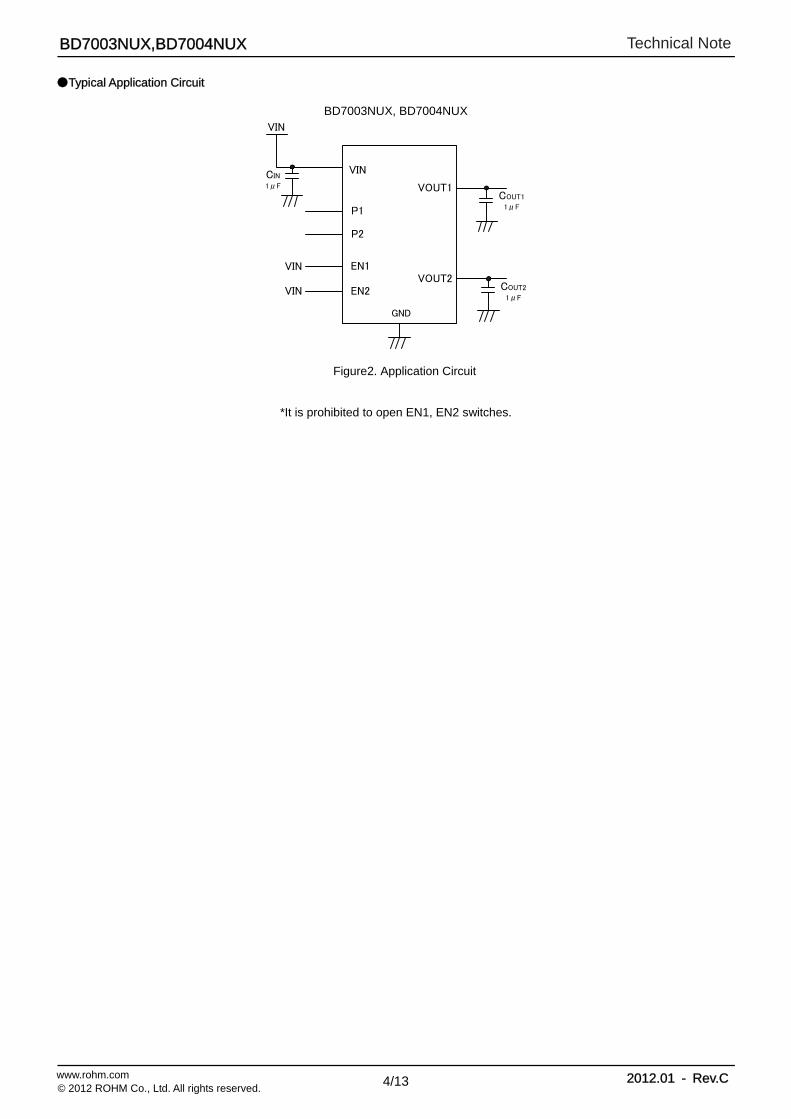
●Typical Application Circuit
BD7003NUX, BD7004NUX
GND
CIN
1μF
VIN
VIN
P1
P2
EN1
EN2VOUT2
VOUT1
VIN
VIN
COUT1
1μF
COUT2
1μF
Figure2. Application Circuit
*It is prohibited to open EN1, EN2 switches.

Technical Note
5/13 www.rohm.com 2012.01 - Rev.C© 2012 ROHM Co., Ltd. All rights reserved.
BD7003NUX,BD7004NUX
●Package Dimensions (VSON008X2020)
Device name Marking
BD7003NUX BD7003
BD7004NUX BD7004
●Pin Descriptions
PIN description (Top View)
Note : Recommend connecting the Thermal Pad to the GND for excellent power dissipation.
PIN No. Name I/O ESD Diode
Function IN GND
1 VIN I - O Voltage Supply
2 EN1 I - O Enable Input1
3 P2 I O O Control Output-Voltage PIN2
4 P1 I O O Control Output-Voltage PIN1
5 EN2 I - O Enable Input2
6 GND - O - GND PIN
7 VOUT2 O - O LDO1 Output1
8 VOUT1 O - O LDO2 Output2
[Unit: mm]
Lot No.
Device name
Technical Note
6/13 www.rohm.com 2012.01 - Rev.C© 2012 ROHM Co., Ltd. All rights reserved.
BD7003NUX,BD7004NUX
●Equivalent Circuit ●Block Diagram
Fig.3. Block Diagram
OVER CURRENTPROTECTION
DISCHARGECIRCUIT
P
ERRORAMP
EN1OUTPUT VOLTAGECONTROL
VREF&
TSD
SHUTDOWNAND POWER- ON
CONTROL
LDO2
2
5
1
8
7
VOUT1
VOUT2
EN2
EN1
VIN
4
3P 2P 1
6GND
LDO 1
VIN
3kΩ
2pin, 5pin (EN)
3kΩ3-StateDecoder
H
OPEN
L
3pin, 4pin (P)
8pin, 7pin (VOUT)

Technical Note
7/13 www.rohm.com 2012.01 - Rev.C© 2012 ROHM Co., Ltd. All rights reserved.
BD7003NUX,BD7004NUX
0
0.2
0.4
0.6
0.8
1
1.2
1.4
1.6
0 0.5 1 1.5 2 2.5 3 3.5 4 4.5 5 5.5
Input Voltage(V)
Ou
tpu
t V
olt
ag
e(V
)
VOUT2=1.5V
Io=300mA
Io=1mA
Io=10mA
Io=0mA
0
0.5
1
1.5
2
2.5
3
3.5
0 0.5 1 1.5 2 2.5 3 3.5 4 4.5 5 5.5
Input Voltage(V)
Ou
tpu
t V
olt
ag
e(V
)
VOUT1=3.3V
Io=300mA
Io=1mA
Io=10mA
Io=0mA
0
0.2
0.4
0.6
0.8
1
1.2
1.4
1.6
2 .5 3 3.5 4 4 .5 5 5 .5
Input Voltage(V)
Ou
tpu
t V
olt
ag
e(V
)
Io=300mA
Io=1mA
Io=10mA
Io=0mA
VOUT2=1.5V
0
0.5
1
1.5
2
2.5
3
3.5
3.7 4.2 4.7 5.2
Input Voltage(V)
Out
put V
olta
ge(V
)
VOUT1=3.3V
Io=300mA
Io=1mA
Io=10mA
Io=0mA
●Typical Operating Characteristics ※The test conditions for the Typical Operating Characteristics are VIN=3.7V, CIN=1.0uF, COUT=1.0uF, Ta=25℃, Unless otherwise noted.
0
20
40
60
80
100
0 0.5 1 1.5 2 2.5 3 3.5 4 4.5 5 5.5
Input Voltage (V)
Gn
d C
urr
en
t (u
A)
Ta=85℃
Ta=25℃
Ta=-40℃
P1=P2=GNDP1=P2=GND
0
1
2
3
4
5
6
7
8
9
10
0 0.5 1 1.5 2 2.5 3 3.5 4 4.5 5 5.5
Input Voltage (V)
Gn
d C
urr
en
t (u
A)
Ta=85℃Ta=25℃Ta=-40℃
P1=P2=GNDP1=P2=GND
0
20
40
60
80
100
0 0.5 1 1.5 2 2.5 3 3.5 4 4.5 5 5.5Input Voltage (V)
Gn
d C
urr
en
t (u
A)
Ta=85℃
Ta=25℃
Ta=-40℃
P1=P2=GNDP1=P2=GND
0
20
40
60
80
100
0 0.5 1 1.5 2 2.5 3 3.5 4 4.5 5 5.5Input Voltage (V)
Gn
d C
urr
en
t (u
A)
Ta=85℃
Ta=25℃
Ta=-40℃
P1=P2=GNDP1=P2=GND
0.0
0.1
0.2
0.3
0.4
0.5
0.6
0.7
0.8
0.9
1.0
0 0.5 1 1.5 2 2.5 3 3.5 4 4.5 5 5.5
Input Voltage (V)
EN
Cu
rre
nt (
uA
)
Ta=85℃
Ta=25℃
Ta=-40℃
P1=P2=GND
0.0
0.1
0.2
0.3
0.4
0.5
0.6
0.7
0.8
0.9
1.0
0 0.5 1 1.5 2 2.5 3 3.5 4 4.5 5 5.5
Input Voltage(V)
EN
Cu
rre
nt
(uA
)
Ta=85℃
Ta=25℃
Ta=-40℃
P1=P2=GND
0
0.2
0.4
0.6
0.8
1
1.2
1.4
0 0.5 1 1.5 2 2.5 3 3.5 4 4.5 5 5.5
Input Voltage(V)
Ou
tpu
t V
olt
ag
e(V
)
Io=300mA
Io=1mA
Io=10mA
Io=0mA
VOUT1=1.2V
0
0.2
0.4
0.6
0.8
1
1.2
1.4
2 .5 3 3.5 4 4 .5 5 5.5
Input Voltage(V)
Ou
tpu
t V
olt
ag
e(V
)
Io=300mA
Io=1mA
Io=10mA
Io=0mAVOUT1=1.2V
Fig.11. Circuit Current (VOUT1=1.8V,VOUT2=2.9V) EN1=VIN, EN2=GND
Fig.10. Circuit Current (VOUT1=1.8V,VOUT2=2.9V)
EN1=EN2=GND
Fig.8. Line Regulation (VOUT2=1.5V)
Fig.7. Line Regulation (VOUT1=1.2V)
Fig.5. Output Voltage (VOUT2=1.5V)
Fig.4. Output Voltage (VOUT1=1.2V)
Fig.12. Circuit Current (VOUT1=1.8V,VOUT2=2.9V)
EN1=GND, EN2=VIN
Fig.13. Circuit Current (VOUT1=1.8V,VOUT2=2.9V)
EN1=EN2=VIN
Fig.6. Output Voltage (VOUT1=3.3V)
Fig.9. Line Regulation (VOUT1=3.3V)
Fig.14. EN1 Input Current Fig.15. EN2 Input Current
Technical Note
8/13 www.rohm.com 2012.01 - Rev.C© 2012 ROHM Co., Ltd. All rights reserved.
BD7003NUX,BD7004NUX
0.0
0.5
1.0
1.5
2.0
2.5
3.0
0 0.5 1 1.5
EN Voltage (V)
Ou
tpu
t Vo
ltag
e (
V)
Ta=85℃
Ta=25℃
Ta=-40℃
0
0.5
1
1.5
2
2.5
3
3.5
4
-40 -15 10 35 60 85Temp [°C]
Vo
ut2
[V
]
Io=0mAIo=0.1mA
0
0.5
1
1.5
2
2.5
3
3.5
4
0 50 100 150 200 250 300
Iout1[A]
VO
UT
1 [V
]
Temp=-40°C Temp=25°C Temp=85°C
0 0.05 0.10 0.15 0.20 0.25 0.30
0
0.5
1
1.5
2
2.5
3
3.5
4
0 50 100 150 200 250 300
Iout2[A]
VO
UT
2 [V
]
0.05 0.1 0.15 0.2 0.25 0.3
Temp=-40°C Temp=25°C Temp=85°C
0
0.5
1
1.5
2
2.5
3
3.5
4
-40 -15 10 35 60 85Temp [°C]
Vo
ut1
[V
]
Io=0mA Io=0.1mA
P1=P2 GN
0.0
0.5
1.0
1.5
2.0
0 0.5 1 1.5
EN Voltage (V)
Ou
tpu
t Vo
ltag
e (
V)
Ta=85℃
Ta=25℃
Ta=-40℃
0
20
40
60
80
100
-40 -15 10 35 60 85
Temp (°C)
Gn
d C
urr
en
t (u
A)
P1=P2=GNDP1=P2=GND P1=P
2 GN
0
20
40
60
80
100
-40 -15 10 35 60 85
Temp (°C)
Gn
d C
urr
en
t (u
A
P1=P2=GNDP1=P2=GND
0
20
40
60
80
100
-40 -15 10 35 60 85
Temp (°C)
Gn
d C
urr
en
t (u
A)
P1=P2=GNDP1=P2=GND
0
1
2
3
4
5
6
7
8
9
10
-40 -15 10 35 60 85
Temp (°C)
Gn
d C
urr
en
t (u
A)
P1=P2=GND
0.00
0.10
0.20
0.30
0.40
0.50
0.60
0.70
0.80
0.90
1.00
0 0.05 0.1 0.15 0.2 0.25 0.3
IOUT(A)
Dro
po
utV
olt
age
(V)
VIN=2.7V
Temp=85℃
Temp=25℃
Temp=-40℃
0.00
0.10
0.20
0.30
0.40
0.50
0.60
0.70
0.80
0.90
1.00
0 0.05 0.1 0.15 0.2 0.25 0.3IOUT(A)
Dro
po
utV
olt
ag
e(V
)
VIN=2.7V
Temp=85℃
Temp=25℃
Temp=-40℃
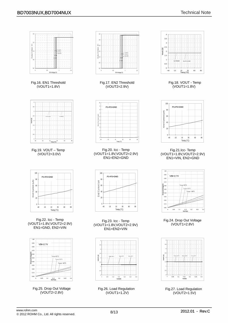
Fig.16. EN1 Threshold (VOUT1=1.8V)
Fig.17. EN2 Threshold (VOUT2=2.9V)
Fig.18. VOUT - Temp (VOUT1=1.8V)
Fig.19. VOUT – Temp (VOUT2=3.0V)
Fig.20. Icc - Temp (VOUT1=1.8V,VOUT2=2.9V)
EN1=EN2=GND
Fig.21.Icc- Temp (VOUT1=1.8V,VOUT2=2.9V)
EN1=VIN, EN2=GND
Fig.22. Icc - Temp (VOUT1=1.8V,VOUT2=2.9V)
EN1=GND, EN2=VIN
Fig.23. Icc - Temp (VOUT1=1.8V,VOUT2=2.9V)
EN1=EN2=VIN
Fig.24. Drop Out Voltage (VOUT1=2.8V)
Fig.25. Drop Out Voltage (VOUT2=2.8V)
Fig.27. Load Regulation (VOUT2=1.5V)
Fig.26. Load Regulation (VOUT1=1.2V)
Technical Note
9/13 www.rohm.com 2012.01 - Rev.C© 2012 ROHM Co., Ltd. All rights reserved.
BD7003NUX,BD7004NUX
0
0.5
1
1.5
2
2.5
3
3.5
4
0 50 100 150 200 250 300Iout1[A]
VO
UT
1 [V
]
Temp=-40°C Temp=25°C Temp=85°C
0
0.5
1
1.5
2
2.5
3
3.5
4
0 50 100 150 200 250 300
Iout2[mA]
VO
UT
2 [V
]
0.05 0.1 0.15 0.2 0.25 0.3
Temo=-40℃ Temo=25℃ Temo=85℃
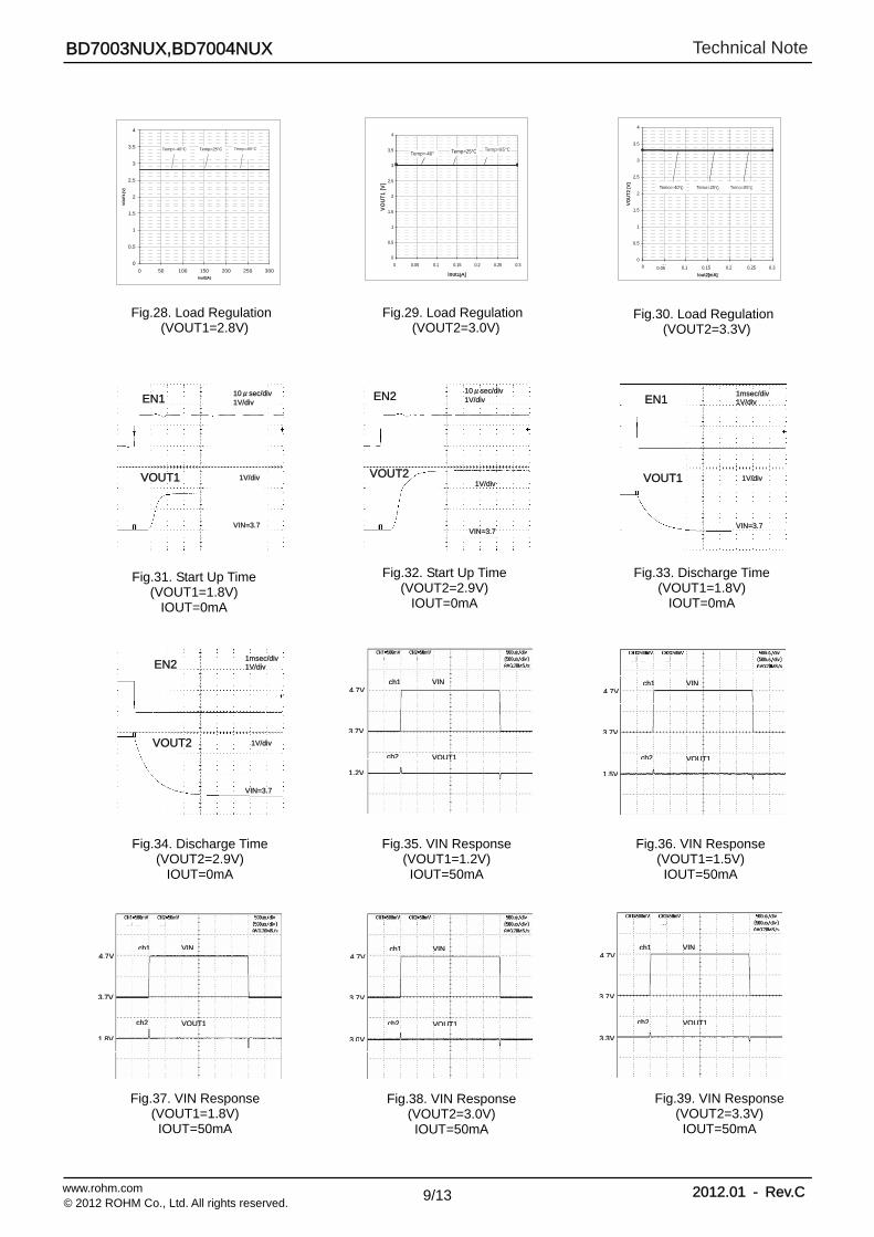
Fig.36. VIN Response (VOUT1=1.5V) IOUT=50mA
Fig.38. VIN Response (VOUT2=3.0V) IOUT=50mA
Fig.39. VIN Response (VOUT2=3.3V) IOUT=50mA
Fig.37. VIN Response (VOUT1=1.8V) IOUT=50mA
Fig.31. Start Up Time (VOUT1=1.8V)
IOUT=0mA
Fig.34. Discharge Time (VOUT2=2.9V)
IOUT=0mA
Fig.32. Start Up Time (VOUT2=2.9V)
IOUT=0mA
Fig.33. Discharge Time (VOUT1=1.8V)
IOUT=0mA
Fig.35. VIN Response (VOUT1=1.2V) IOUT=50mA
0
0.5
1
1.5
2
2.5
3
3.5
4
0 50 100 150 200 250 300
Iout1[A]
VO
UT
1 [V
]
Temp=85°CTemp=25°CTemp=-40°
0 0.05 0.1 0.15 0.2 0.25 0.3
3.7V
1.5V
ch1
ch2
4.7VVIN
VOUT1
3.7V
1.8V
ch1
ch2
4.7VVIN
VOUT1
3.7V
1.2V
ch1
ch2
4.7VVIN
VOUT1
EN2
VOUT2
VIN=3.7
1msec/div 1V/div
1V/div
3.7V
3.0V
ch1
ch2
4.7VVIN
VOUT1
3.7V
3.3V
ch1
ch2
4.7VVIN
VOUT1
EN2
VOUT2
VIN=3.7
10μsec/div 1V/div
1V/div
EN1
VOUT1
VIN=3.7
1msec/div 1V/div
1V/div
EN1
VOUT1
VIN=3.7
10μsec/div 1V/div
1V/div
Fig.28. Load Regulation (VOUT1=2.8V)
Fig.30. Load Regulation (VOUT2=3.3V)
Fig.29. Load Regulation (VOUT2=3.0V)
Technical Note
10/13 www.rohm.com 2012.01 - Rev.C© 2012 ROHM Co., Ltd. All rights reserved.
BD7003NUX,BD7004NUX
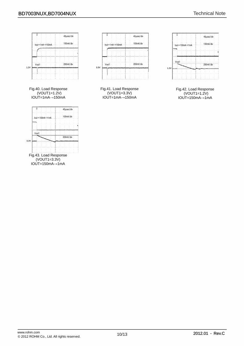
Fig.40. Load Response (VOUT1=1.2V)
IOUT=1mA→150mA
Fig.41. Load Response (VOUT1=3.3V)
IOUT=1mA→150mA
Fig.42. Load Response (VOUT1=1.2V)
IOUT=150mA→1mA
Fig.43. Load Response (VOUT1=3.3V)
IOUT=150mA→1mA
1.2V
Iout=150mA->1mA
Vout1
100mA/div
40μsec/div
200mV/div1.2V
Iout=1mA->150mA
Vout1
100mA/div
40μsec/div
200mV/div
Iout=1mA->150mA
Vout1
100mA/div
40μsec/div
200mV/div
3.3V
Iout=150mA->1mA
Vout1
100mA/div
40μsec/div
200mV/div
3.3V
Technical Note
11/13 www.rohm.com 2012.01 - Rev.C© 2012 ROHM Co., Ltd. All rights reserved.
BD7003NUX,BD7004NUX
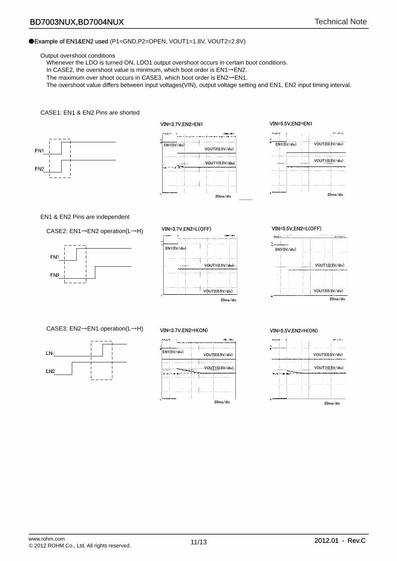
●Example of EN1&EN2 used (P1=GND,P2=OPEN, VOUT1=1.8V, VOUT2=2.8V) Output overshoot conditions
Whenever the LDO is turned ON, LDO1 output overshoot occurs in certain boot conditions. In CASE2, the overshoot value is minimum, which boot order is EN1→EN2. The maximum over shoot occurs in CASE3, which boot order is EN2→EN1. The overshoot value differs between input voltages(VIN), output voltage setting and EN1, EN2 input timing interval.
CASE1: EN1 & EN2 Pins are shorted
EN1 & EN2 Pins are independent
CASE2: EN1→EN2 operation(L→H)
CASE3: EN2→EN1 operation(L→H)
EN1(5V/div)
VIN=3.7V,EN2=EN1
EN1(5V/div)VOUT2(0.5V/div)
VOUT1(0.5V/div)
20ms/div
VIN=5.5V,EN2=EN1
EN1(5V/div)
VOUT1(0.5V/div)
20ms/div
VOUT2(0.5V/div)
VOUT1(0.5V/div)
VOUT2(0.5V/div)
EN1(5V/div)
20ms/div
VIN=3.7V,EN2=L(OFF)
EN1(5V/div)
VOUT1(0.5V/div)
VOUT2(0.5V/div)
20ms/div
VIN=5.5V,EN2=L(OFF)
VOUT2(0.5V/div)
VOUT1(0.5V/div)
20ms/div
VIN=5.5V,EN2=H(ON)
EN1(5V/div)VOUT2(0.5V/div)
VOUT1(0.5V/div)
20ms/div
VIN=3.7V,EN2=H(ON)
Technical Note
12/13 www.rohm.com 2012.01 - Rev.C© 2012 ROHM Co., Ltd. All rights reserved.
BD7003NUX,BD7004NUX
●Notes for use (1) Absolute maximum ratings
If applied voltage (VIN), operating temperature range (Topr), or other absolute maximum ratings are exceeded, there is a risk of damage. Since it is not possible to identify short, open, or other damage modes, if special modes in which absolute maximum ratings are exceeded are assumed, consider applying fuses or other physical safety measures.
(2) Recommended operating range This is the range within which it is possible to obtain roughly the expected characteristics. For electrical characteristics, it is those that are guaranteed under the conditions for each parameter. Even when these are within the recommended operating range, voltage and temperature characteristics are indicated.
(3) Reverse connection of power supply connector There is a risk of damaging the IC by reverse connection of the power supply connector. For protection from reverse connection, take measures such as externally placing a diode between the power supply and the power supply pin of the IC.
(4) Power supply lines In the design of the board pattern, make power supply and GND line wiring low impedance. When doing so, although the digital power supply and analog power supply are the same potential, separate the digital power supply pattern and analog power supply pattern to deter digital noise from entering the analog power supply due to the common impedance of the wiring patterns. Similarly take pattern design into account for GND lines as well. Furthermore, for all power supply pins of the IC, in conjunction with inserting capacitors between power supply and GND pins, when using electrolytic capacitors, determine constants upon adequately confirming that capacitance loss occurring at low temperatures is not a problem for various characteristics of the capacitors used.
(5) GND voltage Make the potential of a GND pin such that it will be the lowest potential even if operating below that. In addition, confirm that there are no pins for which the potential becomes less than a GND by actually including transition phenomena.
(6) Shorts between pins and misinstallation When installing in the set board, pay adequate attention to orientation and placement discrepancies of the IC. If it is installed erroneously, there is a risk of IC damage. There also is a risk of damage if it is shorted by a foreign substance getting between pins , between a pin and a power supply or GND.
(7) Operation in strong magnetic fields Be careful when using the IC in a strong magnetic field, since it may malfunction.
(8) Inspection in set board When inspecting the IC in the set board, since there is a risk of stress to the IC when capacitors are connected to low impedance IC pins, be sure to discharge for each process. Moreover, when getting it on and off of a jig in the inspection process, always connect it after turning off the power supply, perform the inspection, and remove it after turning off the power supply. Furthermore, as countermeasures against static electricity, use grounding in the assembly process and take appropriate care in transport and storage.
(9) Input pins Parasitic elements inevitably are formed on an IC structure due to potential relationships. Because parasitic elements operate, they give rise to interference with circuit operation and may be the cause of malfunctions as well as damage. Accordingly, take care not to apply a lower voltage than GND to an input pin or use the IC in other ways such that parasitic elements operate. Moreover, do not apply a voltage to an input pin when the power supply voltage is not being applied to the IC. Furthermore, when the power supply voltage is being applied, make each input pin a voltage less than the power supply voltage as well as within the guaranteed values of electrical characteristics.
(10) Ground wiring pattern When there is a small signal GND and a large current GND, it is recommended that you separate the large current GND pattern and small signal GND pattern and provide single point grounding at the reference point of the set so that voltage variation due to resistance components of the pattern wiring and large currents do not cause the small signal GND voltage to change. Take care that the GND wiring pattern of externally attached components also does not change.
(11) Externally attached capacitors When using ceramic capacitors for externally attached capacitors, determine constants upon taking into account a lowering of the rated capacitance due to DC bias and capacitance change due to factors such as temperature.
(12) Thermal shutdown circuit (TSD) When the junction temperature becomes 180℃ (typ) or higher, the thermal shutdown circuit operates and turns the switch OFF. The thermal shutdown circuit, which is aimed at isolating the IC from thermal runaway as much as possible, is not aimed at the protection or guarantee of the IC. Therefore, do not continuously use the IC with this circuit operating or use the IC assuming its operation.
(13) Thermal design Perform thermal design in which there are adequate margins by taking into account the permissible dissipation (Pd) in actual states of use.
Technical Note
13/13 www.rohm.com 2012.01 - Rev.C© 2012 ROHM Co., Ltd. All rights reserved.
BD7003NUX,BD7004NUX
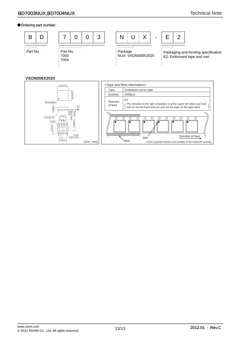
●Ordering part number
B D 7 0 0 3 N U X - E 2
Part No. Part No. 7003 7004
Package NUX: VSON008X2020
Packaging and forming specification E2: Embossed tape and reel
(Unit : mm)
VSON008X2020
2.0±0.05
2.0±0.05
0.6M
AX
0.02
+0.
03−0
.02
S
0.05 S
(0.1
2)
+0.05−0.04
1.5±0.1
1.5±0.1
0.5±0.1
0.8±
0.1
0.3±
0.1
1
8
4
5
C0.25
0.25
1PIN MARK
∗ Order quantity needs to be multiple of the minimum quantity.
<Tape and Reel information>
Embossed carrier tapeTape
Quantity
Direction of feed The direction is the 1pin of product is at the upper left when you hold
reel on the left hand and you pull out the tape on the right hand
4000pcs
E2
( )
Direction of feed
Reel1pin
DatasheetDatasheet
Notice - GE Rev.002© 2014 ROHM Co., Ltd. All rights reserved.
Notice Precaution on using ROHM Products
1. Our Products are designed and manufactured for application in ordinary electronic equipments (such as AV equipment, OA equipment, telecommunication equipment, home electronic appliances, amusement equipment, etc.). If you intend to use our Products in devices requiring extremely high reliability (such as medical equipment (Note 1), transport equipment, traffic equipment, aircraft/spacecraft, nuclear power controllers, fuel controllers, car equipment including car accessories, safety devices, etc.) and whose malfunction or failure may cause loss of human life, bodily injury or serious damage to property (“Specific Applications”), please consult with the ROHM sales representative in advance. Unless otherwise agreed in writing by ROHM in advance, ROHM shall not be in any way responsible or liable for any damages, expenses or losses incurred by you or third parties arising from the use of any ROHM’s Products for Specific Applications.
(Note1) Medical Equipment Classification of the Specific Applications JAPAN USA EU CHINA
CLASSⅢ CLASSⅢ
CLASSⅡb CLASSⅢ
CLASSⅣ CLASSⅢ
2. ROHM designs and manufactures its Products subject to strict quality control system. However, semiconductor
products can fail or malfunction at a certain rate. Please be sure to implement, at your own responsibilities, adequate safety measures including but not limited to fail-safe design against the physical injury, damage to any property, which a failure or malfunction of our Products may cause. The following are examples of safety measures:
[a] Installation of protection circuits or other protective devices to improve system safety [b] Installation of redundant circuits to reduce the impact of single or multiple circuit failure
3. Our Products are designed and manufactured for use under standard conditions and not under any special or extraordinary environments or conditions, as exemplified below. Accordingly, ROHM shall not be in any way responsible or liable for any damages, expenses or losses arising from the use of any ROHM’s Products under any special or extraordinary environments or conditions. If you intend to use our Products under any special or extraordinary environments or conditions (as exemplified below), your independent verification and confirmation of product performance, reliability, etc, prior to use, must be necessary:
[a] Use of our Products in any types of liquid, including water, oils, chemicals, and organic solvents [b] Use of our Products outdoors or in places where the Products are exposed to direct sunlight or dust [c] Use of our Products in places where the Products are exposed to sea wind or corrosive gases, including Cl2,
H2S, NH3, SO2, and NO2
[d] Use of our Products in places where the Products are exposed to static electricity or electromagnetic waves [e] Use of our Products in proximity to heat-producing components, plastic cords, or other flammable items [f] Sealing or coating our Products with resin or other coating materials [g] Use of our Products without cleaning residue of flux (even if you use no-clean type fluxes, cleaning residue of
flux is recommended); or Washing our Products by using water or water-soluble cleaning agents for cleaning residue after soldering
[h] Use of the Products in places subject to dew condensation
4. The Products are not subject to radiation-proof design. 5. Please verify and confirm characteristics of the final or mounted products in using the Products. 6. In particular, if a transient load (a large amount of load applied in a short period of time, such as pulse. is applied,
confirmation of performance characteristics after on-board mounting is strongly recommended. Avoid applying power exceeding normal rated power; exceeding the power rating under steady-state loading condition may negatively affect product performance and reliability.
7. De-rate Power Dissipation (Pd) depending on Ambient temperature (Ta). When used in sealed area, confirm the actual
ambient temperature. 8. Confirm that operation temperature is within the specified range described in the product specification. 9. ROHM shall not be in any way responsible or liable for failure induced under deviant condition from what is defined in
this document.
Precaution for Mounting / Circuit board design 1. When a highly active halogenous (chlorine, bromine, etc.) flux is used, the residue of flux may negatively affect product
performance and reliability. 2. In principle, the reflow soldering method must be used; if flow soldering method is preferred, please consult with the
ROHM representative in advance. For details, please refer to ROHM Mounting specification
DatasheetDatasheet
Notice - GE Rev.002© 2014 ROHM Co., Ltd. All rights reserved.
Precautions Regarding Application Examples and External Circuits 1. If change is made to the constant of an external circuit, please allow a sufficient margin considering variations of the
characteristics of the Products and external components, including transient characteristics, as well as static characteristics.
2. You agree that application notes, reference designs, and associated data and information contained in this document
are presented only as guidance for Products use. Therefore, in case you use such information, you are solely responsible for it and you must exercise your own independent verification and judgment in the use of such information contained in this document. ROHM shall not be in any way responsible or liable for any damages, expenses or losses incurred by you or third parties arising from the use of such information.
Precaution for Electrostatic
This Product is electrostatic sensitive product, which may be damaged due to electrostatic discharge. Please take proper caution in your manufacturing process and storage so that voltage exceeding the Products maximum rating will not be applied to Products. Please take special care under dry condition (e.g. Grounding of human body / equipment / solder iron, isolation from charged objects, setting of Ionizer, friction prevention and temperature / humidity control).
Precaution for Storage / Transportation 1. Product performance and soldered connections may deteriorate if the Products are stored in the places where:
[a] the Products are exposed to sea winds or corrosive gases, including Cl2, H2S, NH3, SO2, and NO2 [b] the temperature or humidity exceeds those recommended by ROHM [c] the Products are exposed to direct sunshine or condensation [d] the Products are exposed to high Electrostatic
2. Even under ROHM recommended storage condition, solderability of products out of recommended storage time period may be degraded. It is strongly recommended to confirm solderability before using Products of which storage time is exceeding the recommended storage time period.
3. Store / transport cartons in the correct direction, which is indicated on a carton with a symbol. Otherwise bent leads
may occur due to excessive stress applied when dropping of a carton. 4. Use Products within the specified time after opening a humidity barrier bag. Baking is required before using Products of
which storage time is exceeding the recommended storage time period.
Precaution for Product Label QR code printed on ROHM Products label is for ROHM’s internal use only.
Precaution for Disposition When disposing Products please dispose them properly using an authorized industry waste company.
Precaution for Foreign Exchange and Foreign Trade act Since our Products might fall under controlled goods prescribed by the applicable foreign exchange and foreign trade act, please consult with ROHM representative in case of export.
Precaution Regarding Intellectual Property Rights 1. All information and data including but not limited to application example contained in this document is for reference
only. ROHM does not warrant that foregoing information or data will not infringe any intellectual property rights or any other rights of any third party regarding such information or data. ROHM shall not be in any way responsible or liable for infringement of any intellectual property rights or other damages arising from use of such information or data.:
2. No license, expressly or implied, is granted hereby under any intellectual property rights or other rights of ROHM or any
third parties with respect to the information contained in this document.
Other Precaution 1. This document may not be reprinted or reproduced, in whole or in part, without prior written consent of ROHM. 2. The Products may not be disassembled, converted, modified, reproduced or otherwise changed without prior written
consent of ROHM. 3. In no event shall you use in any way whatsoever the Products and the related technical information contained in the
Products or this document for any military purposes, including but not limited to, the development of mass-destruction weapons.
4. The proper names of companies or products described in this document are trademarks or registered trademarks of
ROHM, its affiliated companies or third parties.

DatasheetDatasheet
Notice – WE Rev.001© 2014 ROHM Co., Ltd. All rights reserved.
General Precaution 1. Before you use our Pro ducts, you are requested to care fully read this document and fully understand its contents.
ROHM shall n ot be in an y way responsible or liabl e for fa ilure, malfunction or acci dent arising from the use of a ny ROHM’s Products against warning, caution or note contained in this document.
2. All information contained in this docume nt is current as of the issuing date and subj ect to change without any prior
notice. Before purchasing or using ROHM’s Products, please confirm the la test information with a ROHM sale s representative.
3. The information contained in this doc ument is provi ded on an “as is” basis and ROHM does not warrant that all
information contained in this document is accurate an d/or error-free. ROHM shall not be in an y way responsible or liable for any damages, expenses or losses incurred by you or third parties resulting from inaccuracy or errors of or concerning such information.