Embed Size (px)
Citation preview

August 1999 Mixed Signal Products
User’s Guide
SLVU019

IMPORTANT NOTICE
Texas Instruments and its subsidiaries (TI) reserve the right to make changes to their products or to discontinueany product or service without notice, and advise customers to obtain the latest version of relevant informationto verify, before placing orders, that information being relied on is current and complete. All products are soldsubject to the terms and conditions of sale supplied at the time of order acknowledgement, including thosepertaining to warranty, patent infringement, and limitation of liability.
TI warrants performance of its semiconductor products to the specifications applicable at the time of sale inaccordance with TI’s standard warranty. Testing and other quality control techniques are utilized to the extentTI deems necessary to support this warranty. Specific testing of all parameters of each device is not necessarilyperformed, except those mandated by government requirements.
CERTAIN APPLICATIONS USING SEMICONDUCTOR PRODUCTS MAY INVOLVE POTENTIAL RISKS OFDEATH, PERSONAL INJURY, OR SEVERE PROPERTY OR ENVIRONMENTAL DAMAGE (“CRITICALAPPLICATIONS”). TI SEMICONDUCTOR PRODUCTS ARE NOT DESIGNED, AUTHORIZED, ORWARRANTED TO BE SUITABLE FOR USE IN LIFE-SUPPORT DEVICES OR SYSTEMS OR OTHERCRITICAL APPLICATIONS. INCLUSION OF TI PRODUCTS IN SUCH APPLICATIONS IS UNDERSTOOD TOBE FULLY AT THE CUSTOMER’S RISK.
In order to minimize risks associated with the customer’s applications, adequate design and operatingsafeguards must be provided by the customer to minimize inherent or procedural hazards.
TI assumes no liability for applications assistance or customer product design. TI does not warrant or representthat any license, either express or implied, is granted under any patent right, copyright, mask work right, or otherintellectual property right of TI covering or relating to any combination, machine, or process in which suchsemiconductor products or services might be or are used. TI’s publication of information regarding any thirdparty’s products or services does not constitute TI’s approval, warranty or endorsement thereof.
Copyright 1999, Texas Instruments Incorporated
Information About Cautions and Warnings
iii Read This First
Preface
Read This First
About This Manual
This user’s guide describes techniques for designing low dropout voltage lin-ear regulators (LDO) using TI’s SLVP125 evaluation modules (EVM) and TPS76933 LDOs.
How to Use This Manual
This document contains the following chapters:
Chapter 1 Introduction
Chapter 2 EVM Adjustments and Test Points
Chapter 3 Circuit Design
Chapter 4 Test Results
Information About Cautions and Warnings
This book may contain cautions and warnings.
This is an example of a caution statement.
A caution statement describes a situation that could potentiallydamage your software or equipment.
This is an example of a warning statement.
A warning statement describes a situation that could potentiallycause harm to you .
Related Documentation From Texas Instruments
iv
The information in a caution or a warning is provided for your protection.Please read each caution and warning carefully.
Related Documentation From Texas Instruments
TPS760xx, TPS761xx, TPS763xx, TPS764xx, TPS769xx, TPS770xxdata sheets (literature numbers SLVS144B, SLVS178A, SLVS181D,SLVS180A, SLVS203B, SLVS210B)
Running Title—Attribute Reference
v Chapter Title—Attribute Reference
Contents
1 Introduction 1-1. . . . . . . . . . . . . . . . . . . . . . . . . . . . . . . . . . . . . . . . . . . . . . . . . . . . . . . . . . . . . . . . . . . . . 1.1 Low Dropout Voltage Linear Regulator Circuit Operation 1-2. . . . . . . . . . . . . . . . . . . . . . . . . 1.2 Design Strategy 1-3. . . . . . . . . . . . . . . . . . . . . . . . . . . . . . . . . . . . . . . . . . . . . . . . . . . . . . . . . . . . 1.3 Schematic 1-4. . . . . . . . . . . . . . . . . . . . . . . . . . . . . . . . . . . . . . . . . . . . . . . . . . . . . . . . . . . . . . . . . 1.4 Bill of Materials 1-6. . . . . . . . . . . . . . . . . . . . . . . . . . . . . . . . . . . . . . . . . . . . . . . . . . . . . . . . . . . . . 1.5 Board Layout 1-8. . . . . . . . . . . . . . . . . . . . . . . . . . . . . . . . . . . . . . . . . . . . . . . . . . . . . . . . . . . . . .
2 EVM Adjustments and Test Points 2-1. . . . . . . . . . . . . . . . . . . . . . . . . . . . . . . . . . . . . . . . . . . . . . . . 2.1 Adjustment by Switch 2-2. . . . . . . . . . . . . . . . . . . . . . . . . . . . . . . . . . . . . . . . . . . . . . . . . . . . . . . 2.2 Adjustment by Jumper 2-2. . . . . . . . . . . . . . . . . . . . . . . . . . . . . . . . . . . . . . . . . . . . . . . . . . . . . . 2.3 Adjustment by Trimmer 2-2. . . . . . . . . . . . . . . . . . . . . . . . . . . . . . . . . . . . . . . . . . . . . . . . . . . . . . 2.4 Adjustment by Programming Header 2-2. . . . . . . . . . . . . . . . . . . . . . . . . . . . . . . . . . . . . . . . . . 2.5 Test Setup 2-3. . . . . . . . . . . . . . . . . . . . . . . . . . . . . . . . . . . . . . . . . . . . . . . . . . . . . . . . . . . . . . . . .
3 Circuit Design 3-1. . . . . . . . . . . . . . . . . . . . . . . . . . . . . . . . . . . . . . . . . . . . . . . . . . . . . . . . . . . . . . . . . . . 3.1 Adjusting the TPS76x01/TPS77001 Output Voltage 3-2. . . . . . . . . . . . . . . . . . . . . . . . . . . . . 3.2 Temperature Considerations 3-6. . . . . . . . . . . . . . . . . . . . . . . . . . . . . . . . . . . . . . . . . . . . . . . . . 3.3 External Capacitor Requirements – ESR 3-7. . . . . . . . . . . . . . . . . . . . . . . . . . . . . . . . . . . . . . .
4 Test Results 4-1. . . . . . . . . . . . . . . . . . . . . . . . . . . . . . . . . . . . . . . . . . . . . . . . . . . . . . . . . . . . . . . . . . . . . 4.1 Test Results 4-2. . . . . . . . . . . . . . . . . . . . . . . . . . . . . . . . . . . . . . . . . . . . . . . . . . . . . . . . . . . . . . . .

Running Title—Attribute Reference
vi
Figures
1–1 Typical LDO Application 1-2. . . . . . . . . . . . . . . . . . . . . . . . . . . . . . . . . . . . . . . . . . . . . . . . . . . . . . . . 1–2 SLVP125 EVM Universal LDO Tester Schematic Diagram 1-4. . . . . . . . . . . . . . . . . . . . . . . . . . 1–3 Top Layer 1-8. . . . . . . . . . . . . . . . . . . . . . . . . . . . . . . . . . . . . . . . . . . . . . . . . . . . . . . . . . . . . . . . . . . . 1–4 Bottom Layer (top view) 1-8. . . . . . . . . . . . . . . . . . . . . . . . . . . . . . . . . . . . . . . . . . . . . . . . . . . . . . . . 1–5 Assembly Drawing (top assembly) 1-9. . . . . . . . . . . . . . . . . . . . . . . . . . . . . . . . . . . . . . . . . . . . . . . 2–1 Location of Adjustment Parts 2-3. . . . . . . . . . . . . . . . . . . . . . . . . . . . . . . . . . . . . . . . . . . . . . . . . . . 2–2 Test Setup 2-4. . . . . . . . . . . . . . . . . . . . . . . . . . . . . . . . . . . . . . . . . . . . . . . . . . . . . . . . . . . . . . . . . . . 3–1 Programming the TPS76x01/TPS77001 3-2. . . . . . . . . . . . . . . . . . . . . . . . . . . . . . . . . . . . . . . . . . 3–2 Resistor Values 3-3. . . . . . . . . . . . . . . . . . . . . . . . . . . . . . . . . . . . . . . . . . . . . . . . . . . . . . . . . . . . . . . 3–3 Calculated and Measured Maximum Output Current vs Input Voltage
Without Cooling for TPS76933 in Test Setup 3-7. . . . . . . . . . . . . . . . . . . . . . . . . . . . . . . . . . . . . . 3–4 ESR and ESL 3-7. . . . . . . . . . . . . . . . . . . . . . . . . . . . . . . . . . . . . . . . . . . . . . . . . . . . . . . . . . . . . . . . 3–5 LDO Output Stage With Parasitic Resistances ESR and ESL 3-8. . . . . . . . . . . . . . . . . . . . . . . 3–6 Correlation of Different ESRs and Their Influence to the Regulation of Vout at a
Load Step From Low to High Output Current 3-9. . . . . . . . . . . . . . . . . . . . . . . . . . . . . . . . . . . . . 4–1 Rise Time of Function Generator at Gate of MOSFET Q1 (high speed) 4-2. . . . . . . . . . . . . . . 4–2 Rise Time of Function Generator at Gate of MOSFET Q1 (low speed) 4-2. . . . . . . . . . . . . . . 4–3 Transient at Input (Ch1); 4.3 V Input, 3.3 V Output (Ch2) at 100 mA Load,
Cout = 10 mF 4-3. . . . . . . . . . . . . . . . . . . . . . . . . . . . . . . . . . . . . . . . . . . . . . . . . . . . . . . . . . . . . . . . . 4–4 Delay Time EN → Output High 4-3. . . . . . . . . . . . . . . . . . . . . . . . . . . . . . . . . . . . . . . . . . . . . . . . . . 4–5 Full Load (100 mA) – No Load Transition, ∆Vout, Whole Period 4-4. . . . . . . . . . . . . . . . . . . . . 4–6 Full Load (100 mA) – No Load Transition With Cout = 10 µF Electrolytic 4-4. . . . . . . . . . . . . . 4–7 No Load – Full Load (100 mA) Transition With Cout = 10 µF Electrolytic 4-5. . . . . . . . . . . . . .
Tables
1–1 Summary of LDO Families and Their Features 1-3. . . . . . . . . . . . . . . . . . . . . . . . . . . . . . . . . . . . 1–2 SLVP125 EVM Bill of Materials 1-6. . . . . . . . . . . . . . . . . . . . . . . . . . . . . . . . . . . . . . . . . . . . . . . . . 2–1 Jumper Functions 2-2. . . . . . . . . . . . . . . . . . . . . . . . . . . . . . . . . . . . . . . . . . . . . . . . . . . . . . . . . . . . . 2–2 Trimmer Adjustments 2-2. . . . . . . . . . . . . . . . . . . . . . . . . . . . . . . . . . . . . . . . . . . . . . . . . . . . . . . . . . 2–3 Timing Equations 2-3. . . . . . . . . . . . . . . . . . . . . . . . . . . . . . . . . . . . . . . . . . . . . . . . . . . . . . . . . . . . . 3–1 Exact Resistor Values 3-3. . . . . . . . . . . . . . . . . . . . . . . . . . . . . . . . . . . . . . . . . . . . . . . . . . . . . . . . . 3–2 E96 Resistor Series 3-5. . . . . . . . . . . . . . . . . . . . . . . . . . . . . . . . . . . . . . . . . . . . . . . . . . . . . . . . . . .

1-1Introduction
Introduction
This user’s guide describes techniques for designing low dropout (LDO)voltage linear regulators using TI’s SLVP125 evaluation module (EVM) andTPS76933 LDO. LDOs provide ideal power supplies for rapidly transitioningDSP loads such as the Texas Instruments TMS320C54x and similarprocessors, and fast memory. Low quiescent current and very low dropoutvoltage compared to standard LDOs makes the TPS76933 particularlysuitable in battery applications requiring extended lifetime and low cost.
Low noise power supplies, fast transient response, improved efficiency, lowcomponent count, and easy design make LDOs popular in solutions whereswitched converters are too noisy and standard linear regulators are tooinefficient.
Topic Page
1.1 Low Dropout Voltage Linear Regulator Circuit Operation 1–2. . . . . . . . .
1.2 Design Strategy 1–3. . . . . . . . . . . . . . . . . . . . . . . . . . . . . . . . . . . . . . . . . . . . . . .
1.3 Schematic 1–4. . . . . . . . . . . . . . . . . . . . . . . . . . . . . . . . . . . . . . . . . . . . . . . . . . . .
1.4 Bill of Materials 1–6. . . . . . . . . . . . . . . . . . . . . . . . . . . . . . . . . . . . . . . . . . . . . . .
1.5 Board Layout 1–8. . . . . . . . . . . . . . . . . . . . . . . . . . . . . . . . . . . . . . . . . . . . . . . . .
Chapter 1
Low Dropout Voltage Linear Regulator Circuit Operation
1-2
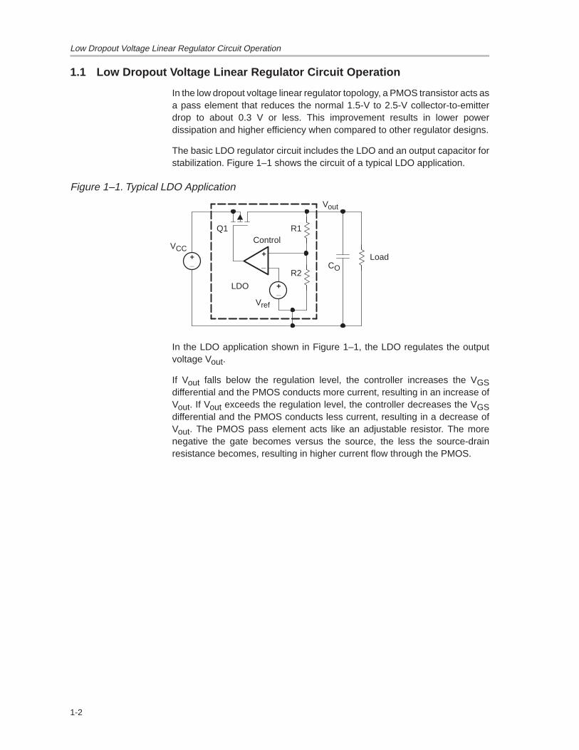
1.1 Low Dropout Voltage Linear Regulator Circuit Operation
In the low dropout voltage linear regulator topology, a PMOS transistor acts asa pass element that reduces the normal 1.5-V to 2.5-V collector-to-emitterdrop to about 0.3 V or less. This improvement results in lower powerdissipation and higher efficiency when compared to other regulator designs.
The basic LDO regulator circuit includes the LDO and an output capacitor forstabilization. Figure 1–1 shows the circuit of a typical LDO application.
Figure 1–1. Typical LDO Application
_+
Control
_+
R1
R2
Q1
Vref
LDO
CO
Vout
Load_+
VCC
In the LDO application shown in Figure 1–1, the LDO regulates the outputvoltage Vout.
If Vout falls below the regulation level, the controller increases the VGSdifferential and the PMOS conducts more current, resulting in an increase ofVout. If Vout exceeds the regulation level, the controller decreases the VGSdifferential and the PMOS conducts less current, resulting in a decrease ofVout. The PMOS pass element acts like an adjustable resistor. The morenegative the gate becomes versus the source, the less the source-drainresistance becomes, resulting in higher current flow through the PMOS.
Design Strategy
1-3Introduction
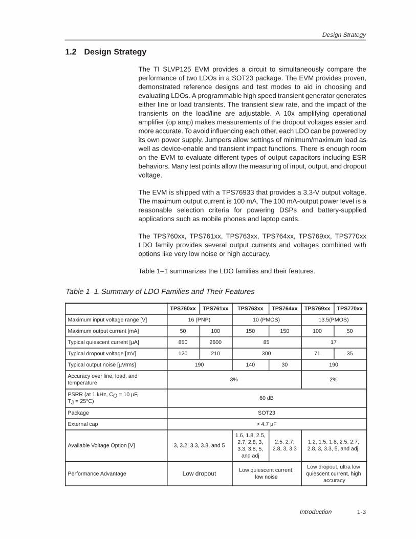
1.2 Design Strategy
The TI SLVP125 EVM provides a circuit to simultaneously compare theperformance of two LDOs in a SOT23 package. The EVM provides proven,demonstrated reference designs and test modes to aid in choosing andevaluating LDOs. A programmable high speed transient generator generateseither line or load transients. The transient slew rate, and the impact of thetransients on the load/line are adjustable. A 10x amplifying operationalamplifier (op amp) makes measurements of the dropout voltages easier andmore accurate. To avoid influencing each other, each LDO can be powered byits own power supply. Jumpers allow settings of minimum/maximum load aswell as device-enable and transient impact functions. There is enough roomon the EVM to evaluate different types of output capacitors including ESRbehaviors. Many test points allow the measuring of input, output, and dropoutvoltage.
The EVM is shipped with a TPS76933 that provides a 3.3-V output voltage.The maximum output current is 100 mA. The 100 mA-output power level is areasonable selection criteria for powering DSPs and battery-suppliedapplications such as mobile phones and laptop cards.
The TPS760xx, TPS761xx, TPS763xx, TPS764xx, TPS769xx, TPS770xxLDO family provides several output currents and voltages combined withoptions like very low noise or high accuracy.
Table 1–1 summarizes the LDO families and their features.
Table 1–1.Summary of LDO Families and Their Features
TPS760xx TPS761xx TPS763xx TPS764xx TPS769xx TPS770xx
Maximum input voltage range [V] 16 (PNP) 10 (PMOS) 13.5(PMOS)
Maximum output current [mA] 50 100 150 150 100 50
Typical quiescent current [µA] 850 2600 85 17
Typical dropout voltage [mV] 120 210 300 71 35
Typical output noise [µVrms] 190 140 30 190
Accuracy over line, load, andtemperature
3% 2%
PSRR (at 1 kHz, CO = 10 µF,TJ = 25°C)
60 dB
Package SOT23
External cap > 4.7 µF
Available Voltage Option [V] 3, 3.2, 3.3, 3.8, and 5
1.6, 1.8, 2.5,2.7, 2.8, 3,3.3, 3.8, 5,
and adj
2.5, 2.7,2.8, 3, 3.3
1.2, 1.5, 1.8, 2.5, 2.7,2.8, 3, 3.3, 5, and adj.
Performance Advantage Low dropoutLow quiescent current,
low noise
Low dropout, ultra lowquiescent current, high
accuracy

Schematic
1-4
1.3 Schematic
Figure1–2 shows the SLVP125 EVM Universal LDO Tester (3.3 V output withTPS76933 as U1) schematic diagram.
Figure 1–2. SLVP125 EVM Universal LDO Tester Schematic Diagram

Schematic
1-5Introduction
Figure 1–2. SLVP125 EVM Universal LDO Tester Schematic Diagram (Continued)
Bill of Materials
1-6
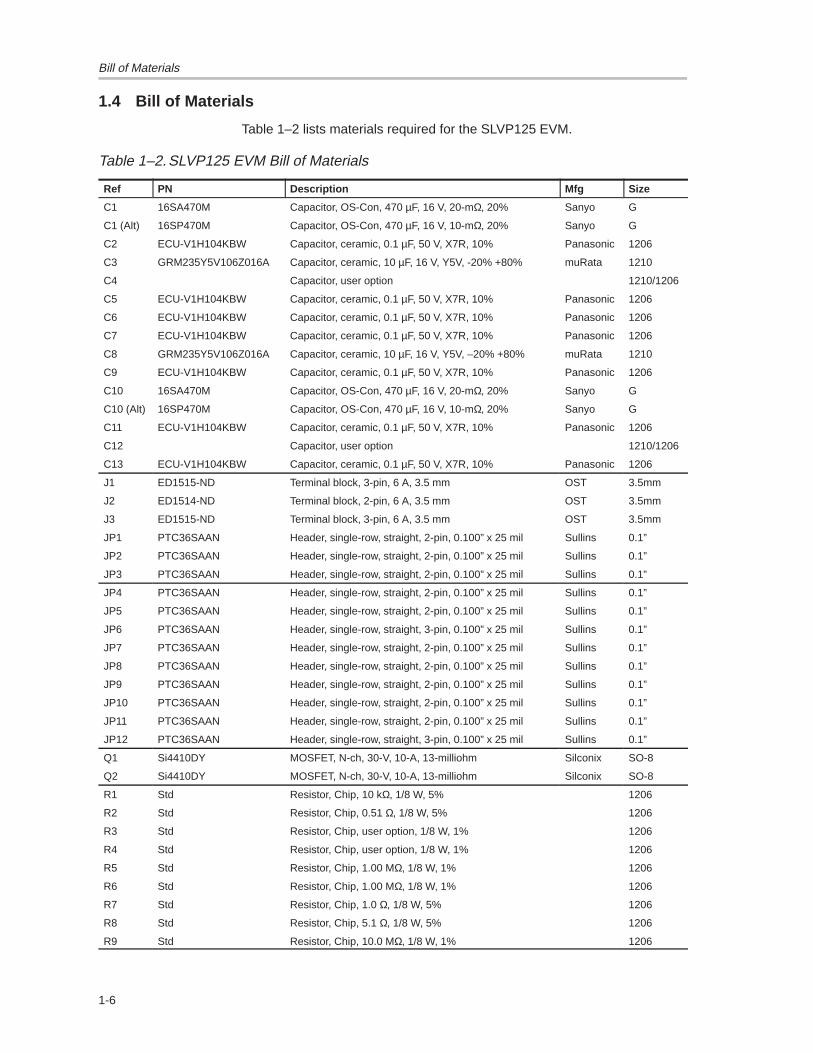
1.4 Bill of Materials
Table 1–2 lists materials required for the SLVP125 EVM.
Table 1–2.SLVP125 EVM Bill of Materials
Ref PN Description Mfg Size
C1 16SA470M Capacitor, OS-Con, 470 µF, 16 V, 20-mΩ, 20% Sanyo G
C1 (Alt) 16SP470M Capacitor, OS-Con, 470 µF, 16 V, 10-mΩ, 20% Sanyo G
C2 ECU-V1H104KBW Capacitor, ceramic, 0.1 µF, 50 V, X7R, 10% Panasonic 1206
C3 GRM235Y5V106Z016A Capacitor, ceramic, 10 µF, 16 V, Y5V, -20% +80% muRata 1210
C4 Capacitor, user option 1210/1206
C5 ECU-V1H104KBW Capacitor, ceramic, 0.1 µF, 50 V, X7R, 10% Panasonic 1206
C6 ECU-V1H104KBW Capacitor, ceramic, 0.1 µF, 50 V, X7R, 10% Panasonic 1206
C7 ECU-V1H104KBW Capacitor, ceramic, 0.1 µF, 50 V, X7R, 10% Panasonic 1206
C8 GRM235Y5V106Z016A Capacitor, ceramic, 10 µF, 16 V, Y5V, –20% +80% muRata 1210
C9 ECU-V1H104KBW Capacitor, ceramic, 0.1 µF, 50 V, X7R, 10% Panasonic 1206
C10 16SA470M Capacitor, OS-Con, 470 µF, 16 V, 20-mΩ, 20% Sanyo G
C10 (Alt) 16SP470M Capacitor, OS-Con, 470 µF, 16 V, 10-mΩ, 20% Sanyo G
C11 ECU-V1H104KBW Capacitor, ceramic, 0.1 µF, 50 V, X7R, 10% Panasonic 1206
C12 Capacitor, user option 1210/1206
C13 ECU-V1H104KBW Capacitor, ceramic, 0.1 µF, 50 V, X7R, 10% Panasonic 1206
J1 ED1515-ND Terminal block, 3-pin, 6 A, 3.5 mm OST 3.5mm
J2 ED1514-ND Terminal block, 2-pin, 6 A, 3.5 mm OST 3.5mm
J3 ED1515-ND Terminal block, 3-pin, 6 A, 3.5 mm OST 3.5mm
JP1 PTC36SAAN Header, single-row, straight, 2-pin, 0.100” x 25 mil Sullins 0.1”
JP2 PTC36SAAN Header, single-row, straight, 2-pin, 0.100” x 25 mil Sullins 0.1”
JP3 PTC36SAAN Header, single-row, straight, 2-pin, 0.100” x 25 mil Sullins 0.1”
JP4 PTC36SAAN Header, single-row, straight, 2-pin, 0.100” x 25 mil Sullins 0.1”
JP5 PTC36SAAN Header, single-row, straight, 2-pin, 0.100” x 25 mil Sullins 0.1”
JP6 PTC36SAAN Header, single-row, straight, 3-pin, 0.100” x 25 mil Sullins 0.1”
JP7 PTC36SAAN Header, single-row, straight, 2-pin, 0.100” x 25 mil Sullins 0.1”
JP8 PTC36SAAN Header, single-row, straight, 2-pin, 0.100” x 25 mil Sullins 0.1”
JP9 PTC36SAAN Header, single-row, straight, 2-pin, 0.100” x 25 mil Sullins 0.1”
JP10 PTC36SAAN Header, single-row, straight, 2-pin, 0.100” x 25 mil Sullins 0.1”
JP11 PTC36SAAN Header, single-row, straight, 2-pin, 0.100” x 25 mil Sullins 0.1”
JP12 PTC36SAAN Header, single-row, straight, 3-pin, 0.100” x 25 mil Sullins 0.1”
Q1 Si4410DY MOSFET, N-ch, 30-V, 10-A, 13-milliohm Silconix SO-8
Q2 Si4410DY MOSFET, N-ch, 30-V, 10-A, 13-milliohm Silconix SO-8
R1 Std Resistor, Chip, 10 kΩ, 1/8 W, 5% 1206
R2 Std Resistor, Chip, 0.51 Ω, 1/8 W, 5% 1206
R3 Std Resistor, Chip, user option, 1/8 W, 1% 1206
R4 Std Resistor, Chip, user option, 1/8 W, 1% 1206
R5 Std Resistor, Chip, 1.00 MΩ, 1/8 W, 1% 1206
R6 Std Resistor, Chip, 1.00 MΩ, 1/8 W, 1% 1206
R7 Std Resistor, Chip, 1.0 Ω, 1/8 W, 5% 1206
R8 Std Resistor, Chip, 5.1 Ω, 1/8 W, 5% 1206
R9 Std Resistor, Chip, 10.0 MΩ, 1/8 W, 1% 1206
Bill of Materials
1-7Introduction
Table 1–2.SLVP125 EVM Bill of Materials (Continued)
Ref PN Description Mfg Size
R10 Std Resistor, Chip, user option, 1/8 W, 1% 1206
R11 Std Resistor, chip, 10.0 MΩ, 1/8 W, 1% 1206
R12 72-T93YA-10 Trim Pot, cermet, 10 Ω vertical, top adjust, 1/2 W, 10% Vishay 3x 0.1”
R13 Std Resistor, chip, user option, 1/8-1 W, 1% 1206/2512
R14 Std Resistor, CF, 5.1 KΩ, 1/8 W, 5% 1206
R15 72-T93YA-50K Trim pot, cermet, 50 KΩ, vertical, top adjust, 1/2 W, 10% Vishay 3x 0.1”
R16 Std Resistor, chip, 10 kΩ, 1/8 W, 5% 1206
R17 Std Resistor, chip, user option, 1/8 W, 5% 1206
R18 Std Resistor, chip, 10 kΩ, 1/8 W, 5% 1206
R19 Std Resistor, chip, user option, 1/8 W, 1% 1206
R20 Std Resistor, chip, 1.0 Ω, 1/8 W, 5% 1206
R21 Std Resistor, chip, user option, 1/8 W, 1% 1206
R22 Std Resistor, chip, 0.51 Ω, 1/8 W, 5% 1206
R23 Std Resistor, chip, 1.00 MΩ, 1/8 W, 1% 1206
R24 Std Resistor, chip, 10.0 MΩ, 1/8 W, 1% 1206
R25 Std Resistor, chip, user option, 1/8 W, 1% 1206
R26 Std Resistor, chip, 1.00 MΩ, 1/8 W, 1% 1206
R27 Std Resistor, chip, 5.1 Ω, 1/8 W, 5% 1206
R28 72-T93YA-10 Trim pot, cermet, 10 Ω, vertical, top adjust, 1/2 W, 10% Vishay 3x 0.1”
R29 Std Resistor, chip, user option, 1/8-1 W, 1% 1206/2512
R30 Std Resistor, chip, 10.0 MΩ, 1/8 W, 1% 1206
R31 Std Resistor, chip, 10 KΩ, 1/8 W, 5% 1206
R32 72-T93YA-50K Trim pot, cermet, 50 KΩ, vertical, top adjust, 1/2 W, 10% Vishay 3x 0.1”
S1 EG1218 Switch, 1P2T, slide, PC-mount E-Switch 0.1”
S2 EG1218 Switch, 1P2T, slide, PC-mount E-Switch 0.1”
S3 EG1218 Switch, 1P2T, slide, PC-mount E-Switch 0.1”
S4 EG1218 Switch, 1P2T, slide, PC-mount E-Switch 0.1”
TP1 131-4244-00 Adaptor, 3.5-mm probe clip (or 131-5031-00) Tektronix
TP2 131-4244-00 Adaptor, 3.5-mm probe clip (or 131-5031-00) Tektronix
TP3 240-345 Test point, red Farnell 1 mm
TP4 240-345 Test point, red Farnell 1 mm
TP5 240-345 Test point, red Farnell 1 mm
TP6 240-333 Test point, black Farnell 1 mm
TP7 240-333 Test point, black Farnell 1 mm
TP8 240-345 Test point, red Farnell 1 mm
TP9 240-345 Test point, red Farnell 1 mm
TP10 240-345 Test point, red Farnell 1 mm
TP11 131-4244-00 Adaptor, 3.5-mm probe clip (or 131-5031-00) Tektronix
TP12 131-4244-00 Adaptor, 3.5-mm probe clip (or 131-5031-00) Tektronix
U1 IC, LDO, DUT TI Various
U2 IC, LDO, DUT TI Various
U3 110-99-316-41-001 Socket, 16-pin, frequency programming Mill-Max DIP-16
U4 TLC555CD IC, CMOS timer TI SO-8
U5 TPS2812D IC, MOSFET driver, 2-Ch, Noninverting TI SO-8
U6 TLE2021CD IC, Op Amp, single-supply, low offset TI SO-8
U7 TLE2021CD IC, Op Amp, single-supply, low offset TI SO-8
Board Layout
1-8
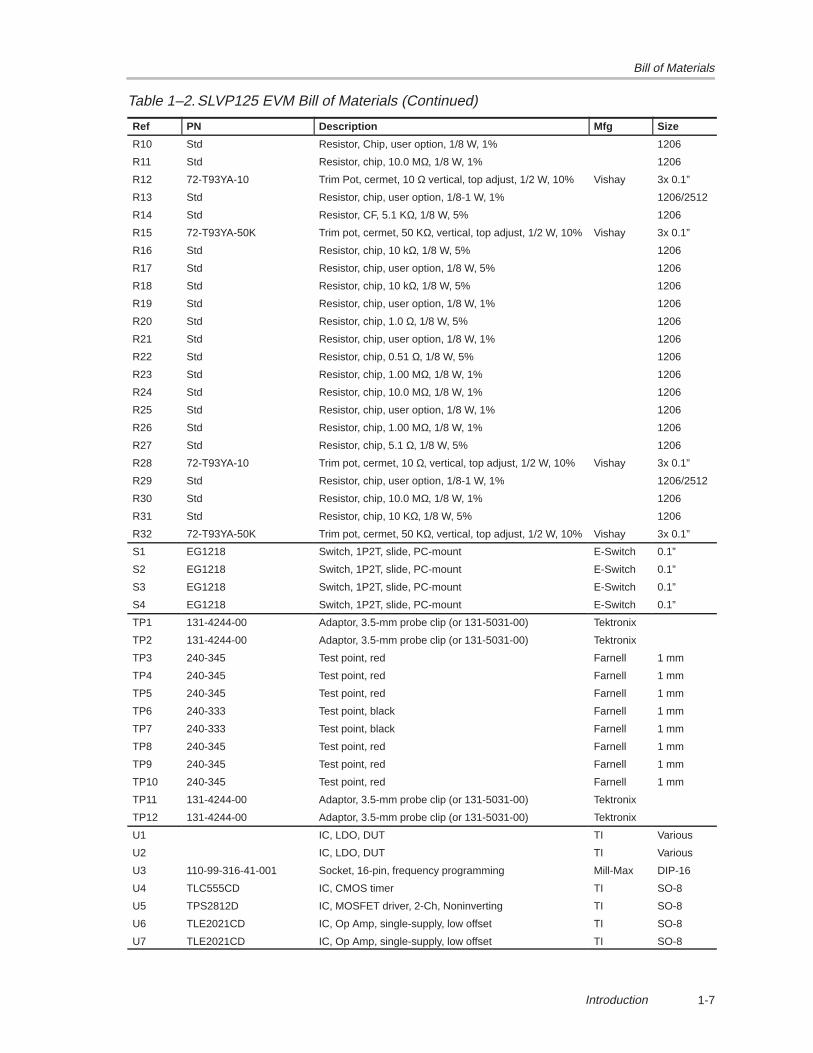
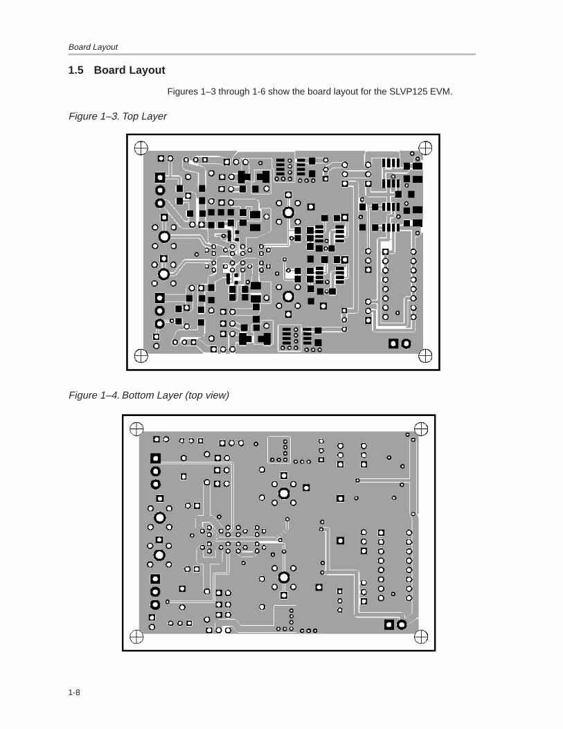
1.5 Board Layout
Figures 1–3 through 1-6 show the board layout for the SLVP125 EVM.
Figure 1–3. Top Layer
Figure 1–4. Bottom Layer (top view)

Board Layout
1-9Introduction
Figure 1–5. Assembly Drawing (top assembly)

1-10
2-1EVM Adjustments and Test Points
EVM Adjustments and Test Points
This chapter explains the following four EVM adjustment modes:
Adjustment by switch Adjustment by jumper Adjustment by trimmer Adjustment by programming header
Figure 2–1 shows the locations of the adjustment points on the board.
Topic Page
2.1 Adjustment by Switch 2–2. . . . . . . . . . . . . . . . . . . . . . . . . . . . . . . . . . . . . . . . .
2.2 Adjustment by Jumper 2–2. . . . . . . . . . . . . . . . . . . . . . . . . . . . . . . . . . . . . . . .
2.3 Adjustment by Trimmer 2–2. . . . . . . . . . . . . . . . . . . . . . . . . . . . . . . . . . . . . . . .
2.4 Adjustment by Programming Header 2–2. . . . . . . . . . . . . . . . . . . . . . . . . . .
2.5 Test Setup 2–3. . . . . . . . . . . . . . . . . . . . . . . . . . . . . . . . . . . . . . . . . . . . . . . . . . . .
Chapter 2

Adjustment by Switch
2-2
2.1 Adjustment by Switch
S1 toggles between high (direction labelling) or low transient generatorfrequency.
S2 switches the transient generator on (direction labelling) and off.
S3 toggles between slower (direction labelling) and faster transients.
S4 directs transients either to DUT1 (direction labelling) or DUT2.
2.2 Adjustment by Jumper
Table 2–1 lists adjustments that can be made by jumpers.
Table 2–1.Jumper Functions
Function/Device DUT1 DUT2
Bypasses input resistor JP1 JP10
Enables DUT JP2 JP7
Bypasses ESR emulation JP3 JP8
Set minimum load JP4 JP9
Set maximum load JP5 JP11
Toggles between input voltage (direction trimmer) and loadtransient
JP6 JP12
2.3 Adjustment by Trimmer
Table 2–2 lists the adjustments that can be made by trimmer.
Table 2–2.Trimmer Adjustments
Function/Device DUT1 DUT2
Risetime of transient R15 R32
Input voltage spike transient impact R12 R28
2.4 Adjustment by Programming Header
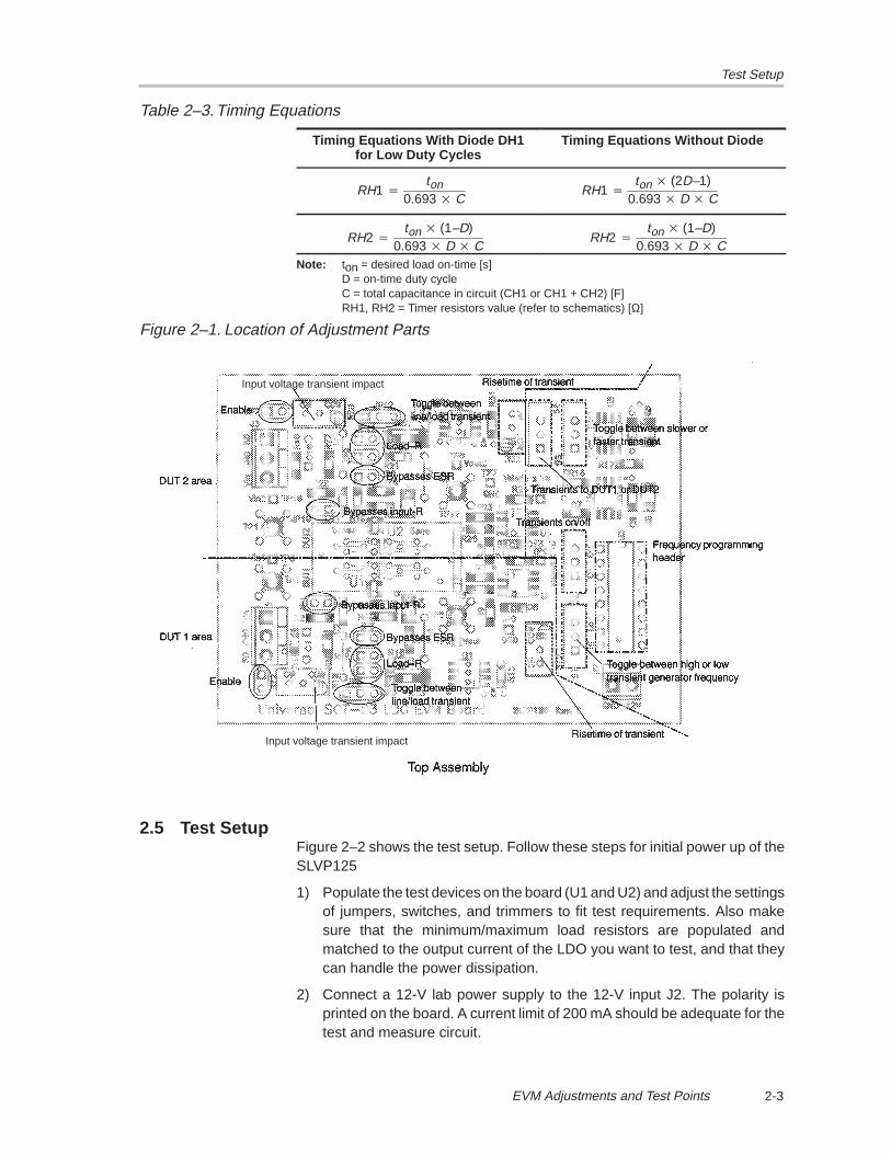
The programming header can be used to program the frequency and the dutycycle of the transient generator. Table 2–3 lists the timing equations.
Test Setup
2-3EVM Adjustments and Test Points
Table 2–3.Timing Equations
Timing Equations With Diode DH1for Low Duty Cycles
Timing Equations Without Diode
RH1ton
0.693CRH1
ton (2D–1)0.693DC
RH2ton (1–D)
0.693DCRH2
ton (1–D)0.693DC
Note: ton = desired load on-time [s]D = on-time duty cycleC = total capacitance in circuit (CH1 or CH1 + CH2) [F]RH1, RH2 = Timer resistors value (refer to schematics) [Ω]
Figure 2–1. Location of Adjustment Parts
Input voltage transient impact
Input voltage transient impact
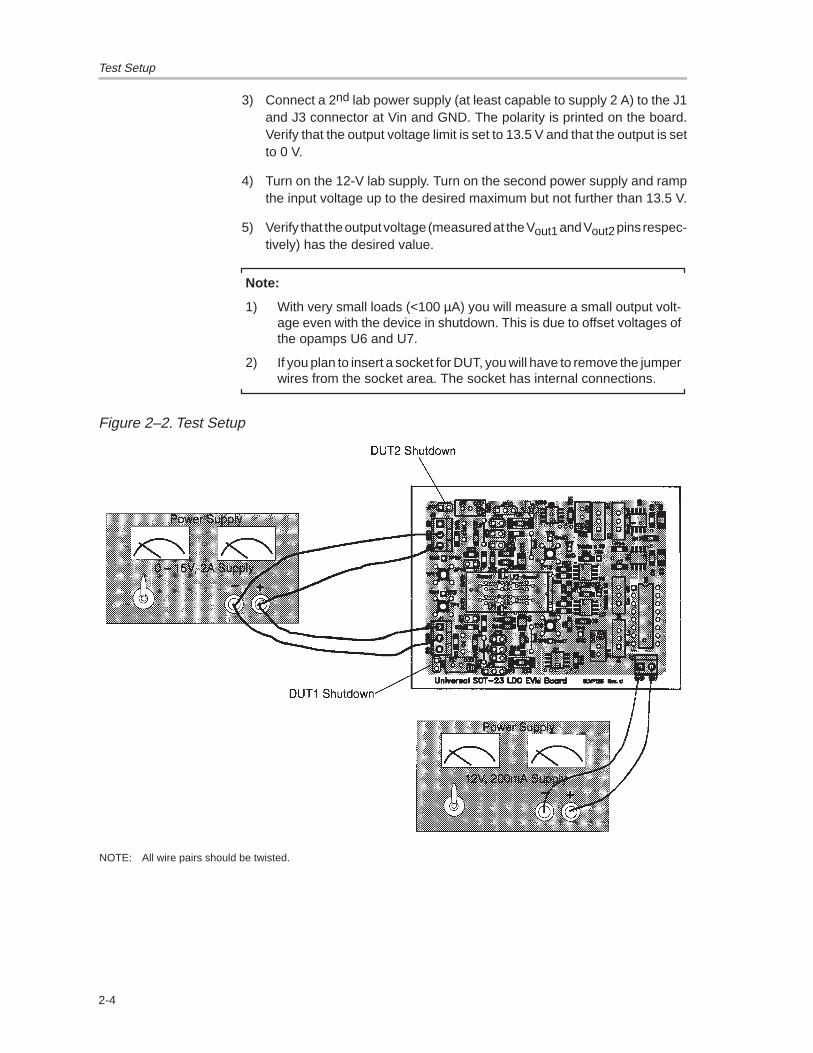
2.5 Test SetupFigure 2–2 shows the test setup. Follow these steps for initial power up of theSLVP125
1) Populate the test devices on the board (U1 and U2) and adjust the settingsof jumpers, switches, and trimmers to fit test requirements. Also makesure that the minimum/maximum load resistors are populated andmatched to the output current of the LDO you want to test, and that theycan handle the power dissipation.
2) Connect a 12-V lab power supply to the 12-V input J2. The polarity isprinted on the board. A current limit of 200 mA should be adequate for thetest and measure circuit.
Test Setup
2-4
3) Connect a 2nd lab power supply (at least capable to supply 2 A) to the J1and J3 connector at Vin and GND. The polarity is printed on the board.Verify that the output voltage limit is set to 13.5 V and that the output is setto 0 V.
4) Turn on the 12-V lab supply. Turn on the second power supply and rampthe input voltage up to the desired maximum but not further than 13.5 V.
5) Verify that the output voltage (measured at the Vout1 and Vout2 pins respec-tively) has the desired value.
Note:
1) With very small loads (<100 µA) you will measure a small output volt-age even with the device in shutdown. This is due to offset voltages ofthe opamps U6 and U7.
2) If you plan to insert a socket for DUT, you will have to remove the jumperwires from the socket area. The socket has internal connections.
Figure 2–2. Test Setup
NOTE: All wire pairs should be twisted.

3-1Circuit Design
Circuit Design
This chapter describes the LDO circuit design procedure.
Topic Page
3.1 Adjusting the TPS76xx01/TPS77001 Output Voltage 3–2. . . . . . . . . . . . .
3.2 Temperature Considerations 3–6. . . . . . . . . . . . . . . . . . . . . . . . . . . . . . . . . . .
3.3 External Capacitor Requirements – ESR 3–7. . . . . . . . . . . . . . . . . . . . . . . .
Chapter 3

Adjusting the TPS76x01/TPS77001 Output Voltage
3-2
3.1 Adjusting the TPS76x01/TPS77001 Output Voltage
All voltage regulators of the TPS76x01/TPS77001 families use the same inter-nal bandgap voltage, see also Figure 1–1. In the adjustable version, the resis-tors R1 and R2 are external resistors. Due to the virtual short circuit betweenthe input pins of an op amp, the voltage Vref applies to both the +input pin andthe –input pin.
Note:
All TPS76x01/TPS77001 devices except the TPS764xx use pin 4 as a feed-back pin for the adjustable version. At the TPS764xx pin 4 acts as a bypasspin for an external bypass capacitor. This capacitor is used to further reduceoutput voltage noise. See the TPS764xx data sheet for details.
Figure 3–1. Programming the TPS76x01/TPS77001
_+
_+
R1
R2
Vref
Vout
The equation for the output voltage is:
VrefVout
R2R1R2
Vout VrefR1R2
R2 Vref1R1
R2
The resistor ratio is a function of
VoutVref
1 R1R2
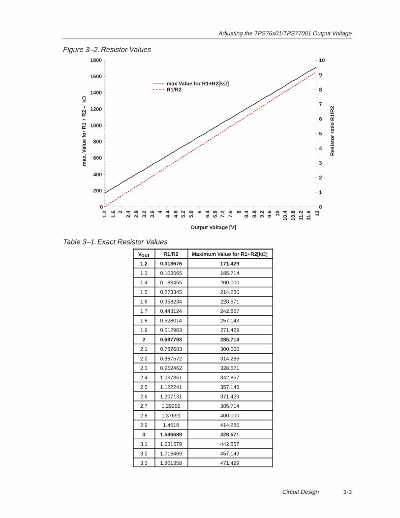
Using Figure 3–2, it is possible to get a quick ratio for R1/R2 and their maxi-mum value.
Adjusting the TPS76x01/TPS77001 Output Voltage
3-3Circuit Design
Figure 3–2. Resistor Values
0
200
400
600
800
1000
1200
1400
1600
1800
Output Voltage [V]
0
1
2
3
4
5
6
7
8
9
10
max Value for R1+R2[k Ω]R1/R2
1.2
1.6 2
2.4
2.8
3.2
3.6 4
4.4
4.8
5.2
5.6 6
6.4
6.8
7.2
7.6 8
8.4
8.8
9.2 10
10.4
10.8
11.2
11.6 129.6
max
. Val
ue fo
r R
1 +
R2
– k
Res
isto
r ra
tio R
1/R
2
Ω
Table 3–1.Exact Resistor Values
Vout R1/R2 Maximum Value for R1+R2[k Ω]
1.2 0.018676 171.429
1.3 0.103565 185.714
1.4 0.188455 200.000
1.5 0.273345 214.286
1.6 0.358234 228.571
1.7 0.443124 242.857
1.8 0.528014 257.143
1.9 0.612903 271.429
2 0.697793 285.714
2.1 0.782683 300.000
2.2 0.867572 314.286
2.3 0.952462 328.571
2.4 1.037351 342.857
2.5 1.122241 357.143
2.6 1.207131 371.429
2.7 1.29202 385.714
2.8 1.37691 400.000
2.9 1.4618 414.286
3 1.546689 428.571
3.1 1.631579 442.857
3.2 1.716469 457.143
3.3 1.801358 471.429

Adjusting the TPS76x01/TPS77001 Output Voltage
3-4
Table 3–1. Exact Resistor Values(Continued)
Vout R1/R2 Maximum Value for R1+R2[k Ω]
3.4 1.886248 485.714
3.5 1.971138 500.000
3.6 2.056027 514.286
3.7 2.140917 528.571
3.8 2.225806 542.857
3.9 2.310696 557.143
4 2.395586 571.429
4.1 2.480475 585.714
4.2 2.565365 600.000
4.3 2.650255 614.286
4.4 2.735144 628.571
4.5 2.820034 642.857
4.6 2.904924 657.143
4.7 2.989813 671.429
4.8 3.074703 685.714
4.9 3.159593 700.000
5 3.244482 714.286
5.5 3.66893 785.714
6 4.093379 857.143
6.5 4.517827 928.571
7 4.942275 1000.000
7.5 5.366723 1071.429
8 5.791171 1142.857
8.5 6.21562 1214.286
9 6.640068 1285.714
9.5 7.064516 1357.143
10 7.488964 1428.571
10.5 7.913413 1500.000
11 8.337861 1571.429
11.5 8.762309 1642.857
12 9.186757 1714.286
To ensure proper regulation, the divider current should be 7 µA. The maximumresistor value for R1+R2 can be seen in Figure 3–2 and Table 3–1.
To get the actual values for R1 and R2, get the resistor ratio and the maximumresistor value for the desired output voltage out of Figure 3–2 or Table 3–1 anddo the following calculations:
Adjusting the TPS76x01/TPS77001 Output Voltage
3-5Circuit Design
For 3 V, one gets:
I) R1R2
1.546689 II) R1R2 428.571 k
I) R1 1.546689R2
I) in II) : 1.546689R2R2 428.571 k
R2 428.571 k2.546689
168.286 k
Make R2 = 169 kΩ and calculate R1:
Derived from equation I), one gets for R1:
R1 1.546689 169 k 261.39 k
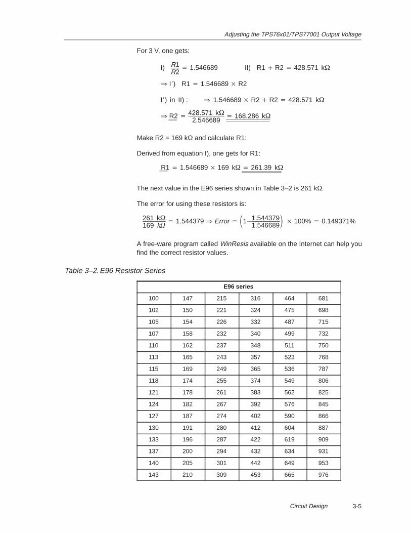
The next value in the E96 series shown in Table 3–2 is 261 kΩ.
The error for using these resistors is:
261 k169 k
1.544379 Error 1– 1.5443791.546689
100% 0.149371%
A free-ware program called WinResis available on the Internet can help youfind the correct resistor values.
Table 3–2.E96 Resistor Series
E96 series
100 147 215 316 464 681
102 150 221 324 475 698
105 154 226 332 487 715
107 158 232 340 499 732
110 162 237 348 511 750
113 165 243 357 523 768
115 169 249 365 536 787
118 174 255 374 549 806
121 178 261 383 562 825
124 182 267 392 576 845
127 187 274 402 590 866
130 191 280 412 604 887
133 196 287 422 619 909
137 200 294 432 634 931
140 205 301 442 649 953
143 210 309 453 665 976
Temperature Considerations
3-6
3.2 Temperature Considerations
To protect the device and assure the specifications, the maximum junctiontemperature should not exceed 125°C. This restriction limits the power dis-sipation the regulator can handle in any given application. To ensure the junc-tion temperature is within acceptable limits, calculate the maximum allowabledissipation, PD(max), and the actual dissipation, PD, which must be less thanor equal to PD(max). The maximum power dissipation limit is determined usingthe following equation:
PD(max) TJ,max TA
RJA
Where
TJ,max is the maximum allowed junction temperature [°C], i.e., 125°C for
the TPS76xxx/TPS77xxx families
RθJA is the thermal resistance junction-to-ambient for the package, i.e.,
285°C/W for the 5-terminal SOT23
TA is the ambient temperature
The regulator dissipation is calculated using:
PD VIN VOUT IOUT
The maximum output current at a given temperature can be calculated as:
Iout,max[mA] 125°C TA
Vin Vout 285°CW 1000 mA
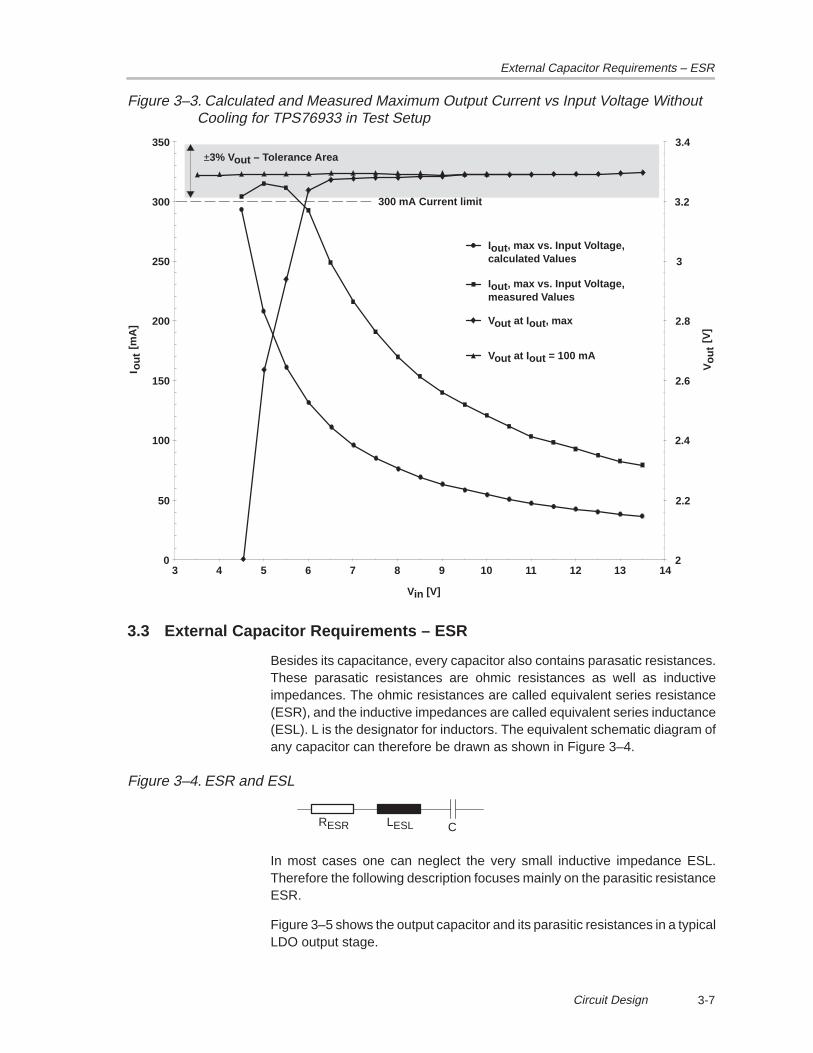
Figure 3–3 shows the test results on a TPS76933 device. Also displayed arethe calculated results.
External Capacitor Requirements – ESR
3-7Circuit Design
Figure 3–3. Calculated and Measured Maximum Output Current vs Input Voltage WithoutCooling for TPS76933 in Test Setup
0
50
100
150
200
250
3 4
Vin [V]
±3% Vout – Tolerance Area
I out
[mA
]
300 mA Current limit
Vou
t[V
]
300
350
2
2.2
2.4
2.6
2.8
3
3.2
3.4
5 6 7 8 9 10 11 12 13 14
Iout , max vs. Input Voltage,calculated Values
Iout , max vs. Input Voltage,measured Values
Vout at Iout , max
Vout at Iout = 100 mA
3.3 External Capacitor Requirements – ESR
Besides its capacitance, every capacitor also contains parasatic resistances.These parasatic resistances are ohmic resistances as well as inductiveimpedances. The ohmic resistances are called equivalent series resistance(ESR), and the inductive impedances are called equivalent series inductance(ESL). L is the designator for inductors. The equivalent schematic diagram ofany capacitor can therefore be drawn as shown in Figure 3–4.
Figure 3–4. ESR and ESL
RESR LESL C
In most cases one can neglect the very small inductive impedance ESL.Therefore the following description focuses mainly on the parasitic resistanceESR.
Figure 3–5 shows the output capacitor and its parasitic resistances in a typicalLDO output stage.

External Capacitor Requirements – ESR
3-8
Figure 3–5. LDO Output Stage With Parasitic Resistances ESR and ESL
LDO
Vin
VESR
VCout
Iout
RESR
LESL
Cout
RLOADVout
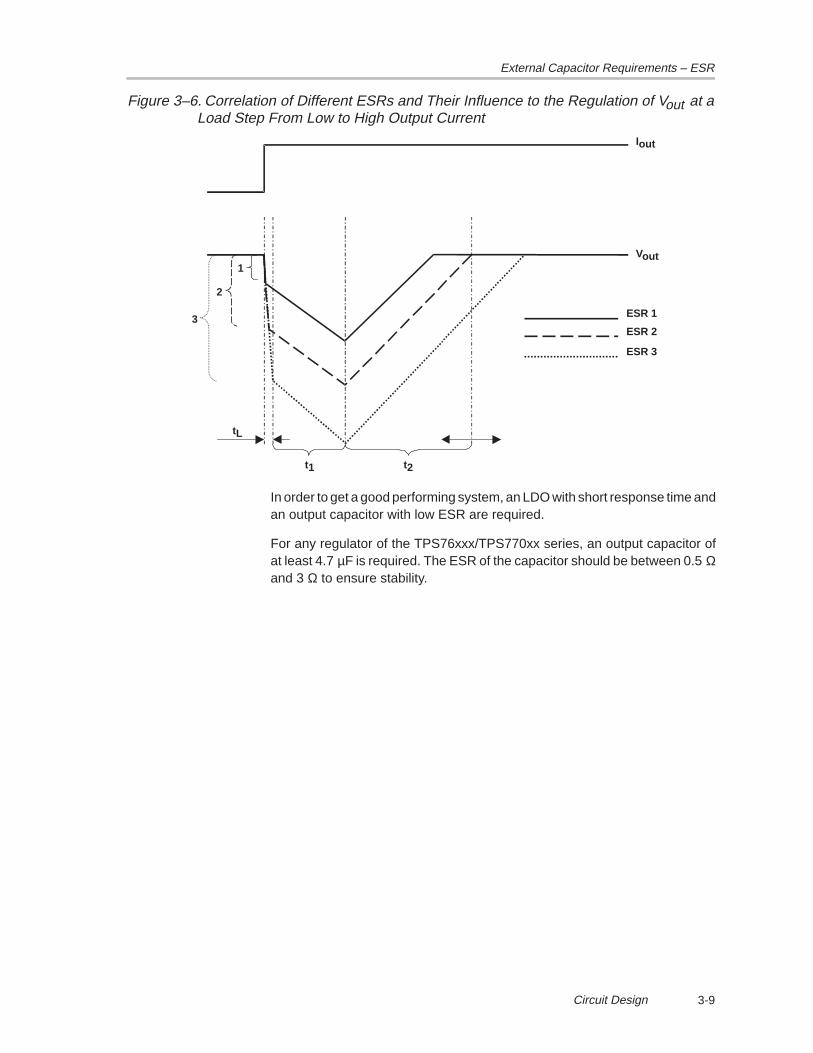
In steady state (dc state condition) the load is supplied by the LDO (solid arrow)and VCout = Vout. This means no current is flowing into the Cout branch. If nowIout suddenly increases, the following occurs (see Figure 3–6 and the screenshot in Chapter 4, Figure 4–7):
The LDO is not able to supply the sudden current need due to its response time(t1 in Figure 3–6). Therefore capacitor Cout has to provide the current for thenew load condition (dashed arrow). Cout acts like a battery now with an internalresistance, ESR. Therefore, depending on the current demand at the output,voltage drop will occur at RESR and LESL. This voltage is shown as VESR in Fig-ure 3–5. The internal inductance also causes an additional delay (shown astL in Figure 3–6), so Cout could not immediately supply current to the load.When Cout is finally conducting current to the load, the initial voltage at the loadwill be Vout = VCout – VESR. Due to the discharge of Cout, the output voltage Voutwill drop continuously until the response time t1 of the LDO is reached and theLDO will resume supplying the load. From this point the output voltage startsrising again until it reaches the level directed by the LDO. This period is shownas t2 in Figure 3–6. The figure also shows the impact of different ESRs on theoutput voltage. The left brackets show different levels of ESRs where number1 displays the lowest and number 3 displays the highest ESR.
Understanding the above, one can draw the following conclusions:
The higher the ESR, the bigger the spike at the beginning of a load tran-sient and the longer the time to return to a steady state.
The smaller the output capacitor, the faster the discharge time and thebigger the voltage loss during the LDO response period (shown as t1 inFigure 3–6).
Conclusion:
The higher the output current and the load step differentials, the higher therequirements for a Cout with low ESR.
External Capacitor Requirements – ESR
3-9Circuit Design
Figure 3–6. Correlation of Different ESRs and Their Influence to the Regulation of Vout at aLoad Step From Low to High Output Current
ESR 1
ESR 2
ESR 3
3
1
2
tL
t1 t2
Iout
Vout
In order to get a good performing system, an LDO with short response time andan output capacitor with low ESR are required.
For any regulator of the TPS76xxx/TPS770xx series, an output capacitor ofat least 4.7 µF is required. The ESR of the capacitor should be between 0.5 Ωand 3 Ω to ensure stability.

3-10

4-1Test Results
Test Results
This chapter presents laboratory test results for the LDO design.
Topic Page
4.1 Test Results 4–2
Chapter 4

Test Results
4-2
4.1 Test Results
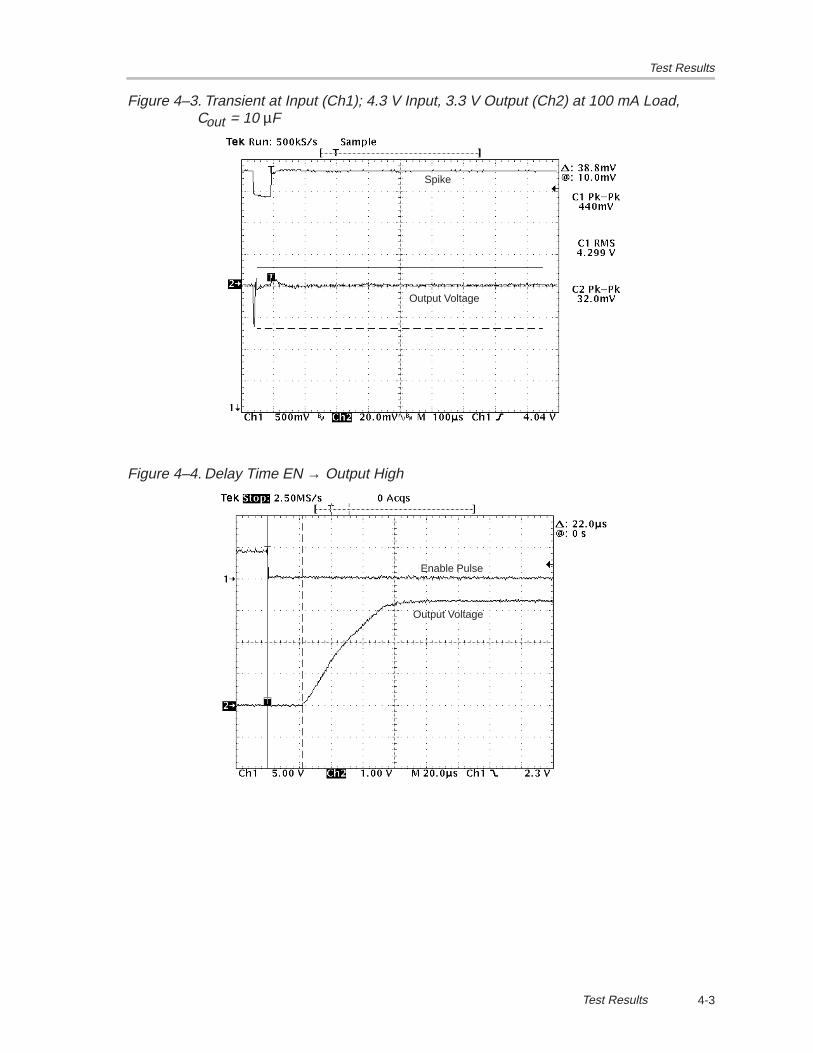
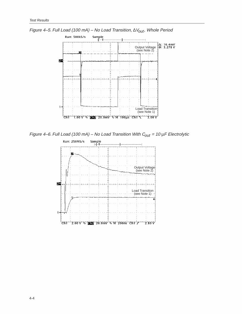
Figures 4–1 through 4–7 show the results of various tests and test conditionsfor the circuit using the TPS76933 device.
Figure 4–1. Rise Time of Function Generator at Gate of MOSFET Q1 (high speed)
Figure 4–2. Rise Time of Function Generator at Gate of MOSFET Q1 (low speed)
Test Results
4-3Test Results
Figure 4–3. Transient at Input (Ch1); 4.3 V Input, 3.3 V Output (Ch2) at 100 mA Load,Cout = 10 µF
Spike
Output Voltage
Figure 4–4. Delay Time EN → Output High
Enable Pulse
Output Voltage
Test Results
4-4
Figure 4–5. Full Load (100 mA) – No Load Transition, ∆Vout , Whole Period
Load Transition
Output Voltage(see Note 2)
(see Note 1)
Figure 4–6. Full Load (100 mA) – No Load Transition With Cout = 10 µF Electrolytic
Load Transition
Output Voltage(see Note 2)
(see Note 1)

Test Results
4-5Test Results
Figure 4–7. No Load – Full Load (100 mA) Transition With Cout = 10 µF Electrolytic
Load Transition
Output Voltage(see Note 2)
(see Note 1)
Notes: 1) The load transition was measured as the voltage drop at the drain of Q1(see Figure 1–2). Therefore load on is displayed as 0 V and load off isdisplayed as 3.3 V.
2) In order to display the output voltage transient with high resolution, a dcoffset of 3.3 V was introduced. The actual dc values can be seen with thecursor lines in Figure 4–5.output voltage without full load: 3.296 Voutput voltage with full load: 3.278 V

4-6