Embed Size (px)
Citation preview
6.012 - Microelectronic Devices and Circuits - Fall 2005 Lecture 14-1
Lecture 14 - Digital Circuits (III)
CMOS
October 27, 2005
Contents:
1. Complementary MOS (CMOS) inverter: introduction
2. CMOS inverter: noise margins
3. CMOS inverter: propagation delay
4. CMOS inverter: dynamic power
Reading assignment:
Howe and Sodini, Ch. 5, §5.4
Announcements:
• Cadence tutorial by Kerwin Johnson in place of reg-ular recitations on Friday 10/28
6.012 - Microelectronic Devices and Circuits - Fall 2005 Lecture 14-2
Key questions
• How does CMOS work?
• What is special about CMOS as a logic technology?
• What are the key design parameters of a CMOS in-verter?
• How can one estimate the propagation delay of a CMOS inverter?
• Does CMOS burn any power?
6.012 - Microelectronic Devices and Circuits - Fall 2005 Lecture 14-3
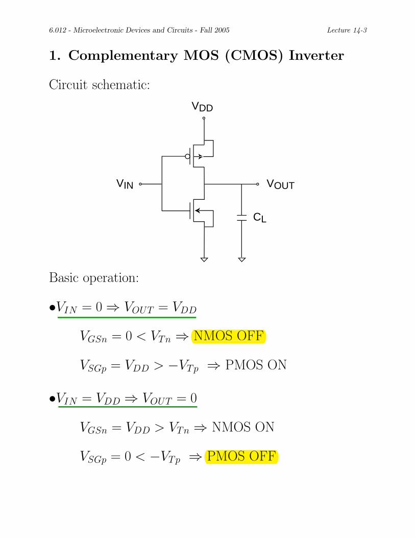
1. Complementary MOS (CMOS) Inverter
Circuit schematic:
VDD
VIN VOUT
CL
Basic operation:
•VIN = 0 ⇒ VOU T = VDD
VGSn = 0 < VTn ⇒ NMOS OFFNMOS OFF
VSGp = VDD > −VTp ⇒ PMOS ON
•VIN = VDD ⇒ VOU T = 0
VGSn = VDD > VTn ⇒ NMOS ON
VSGp = 0 < −VTp ⇒ PMOS OFFPMOS OFF
6.012 - Microelectronic Devices and Circuits - Fall 2005 Lecture 14-4
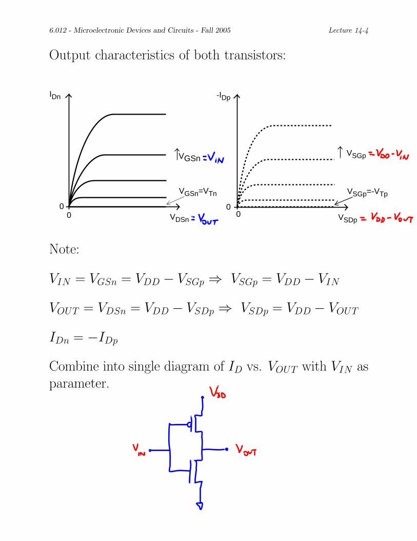
Output characteristics of both transistors:
IDn
0 VSDp
-IDp
VSGp
VSGp=-VTp
0 0VDSn
VGSn
VGSn=VTn
0
Note:
VIN = VGSn = VDD − VSGp ⇒ VSGp = VDD − VIN
VOU T = VDSn = VDD − VSDp ⇒ VSDp = VDD − VOU T
IDn = −IDp
Combine into single diagram of ID vs. VOU T with VIN as parameter.
VV
current while id in lo state
ail-to-rail” lo lo levels are
6.012 - Microelectronic Devices and Circuits - Fall 2005 Lecture 14-5
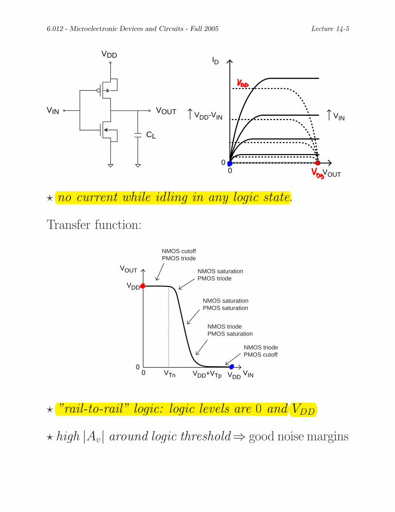
VDD ID
VIN VOUT VDD-VIN VIN
CL
0 0 VOUT
� no ling any gic .no current while idling in any logic state.
Transfer function:
NMOS cutoff
VOUT
0
VDD
PMOS triode
NMOS saturation PMOS triode
NMOS saturation PMOS saturation
NMOS triode PMOS saturation
NMOS triode PMOS cutoff
0 VTn VDD+VTp VDD VIN
� ”r gic: gic 0 and VDD”rail-to-rail” logic: logic levels are 0 and VDD
� high |Av| around logic threshold ⇒ good noise margins
6.012 - Microelectronic Devices and Circuits - Fall 2005 Lecture 14-6
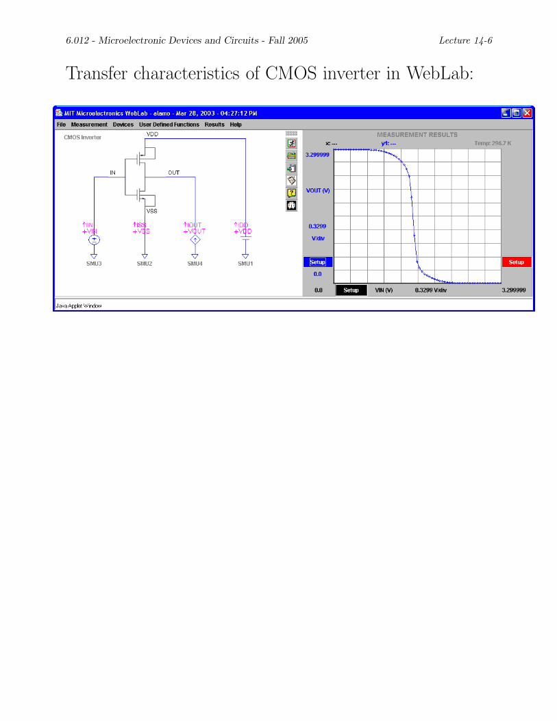
Transfer characteristics of CMOS inverter in WebLab:
6.012 - Microelectronic Devices and Circuits - Fall 2005 Lecture 14-7
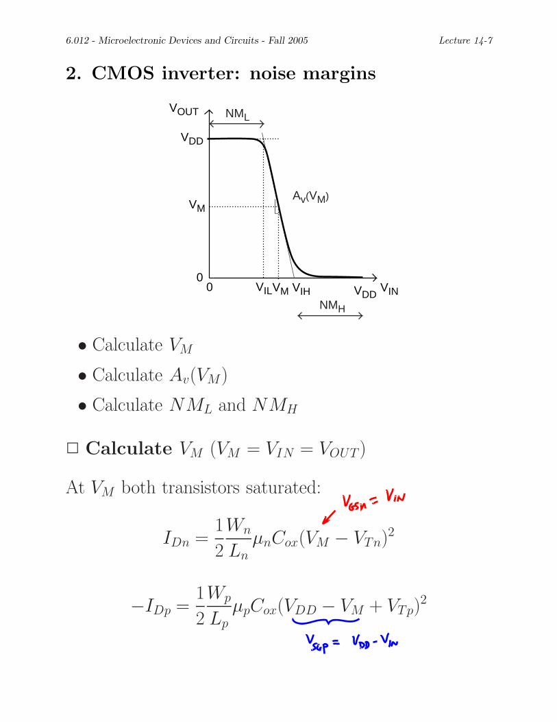
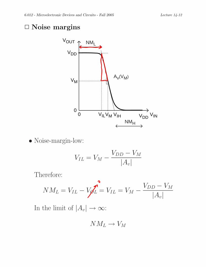
2. CMOS inverter: noise margins
VOUT
VDD
VM
0
Av(VM)
NML
0 VILVM VIH VDD VIN
NMH
• Calculate VM
• Calculate Av(VM )
• Calculate NML and NMH
2 Calculate VM (VM = VIN = VOU T )
At VM both transistors saturated:
1 WnIDn = µnCox(VM − VTn)
2
2 Ln
1 Wp−IDp = µpCox(VDD − VM + VTp)2
2 Lp
VV
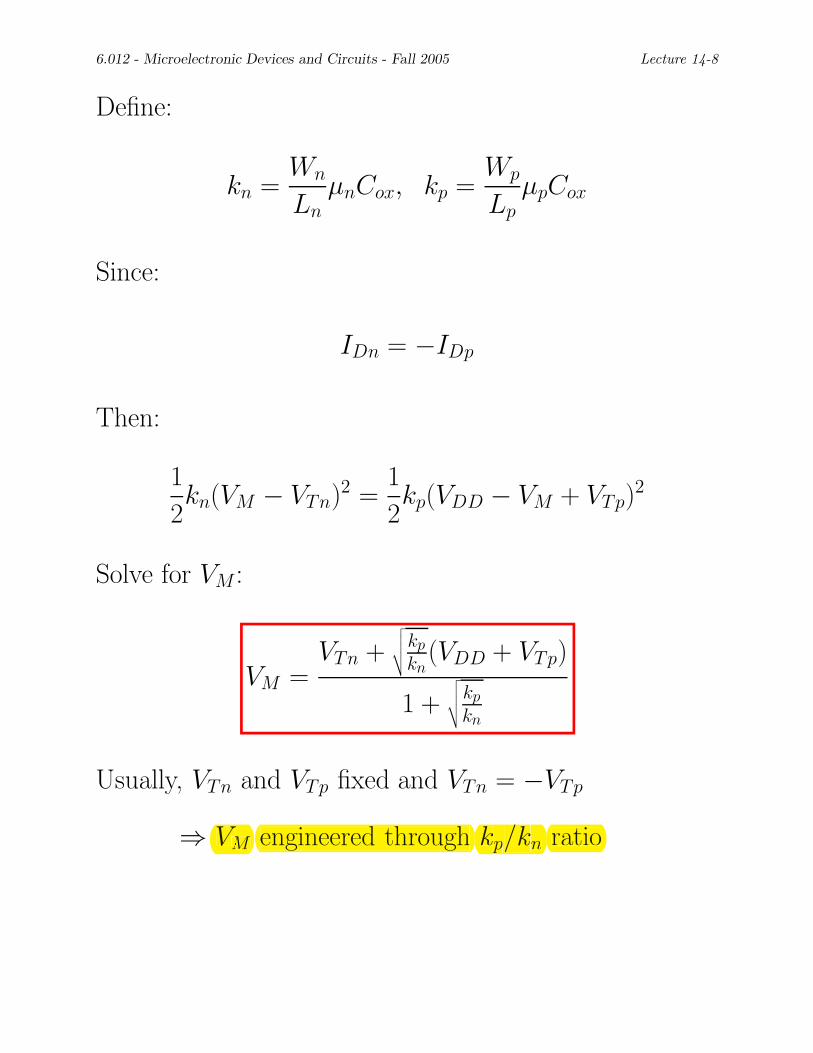
6.012 - Microelectronic Devices and Circuits - Fall 2005 Lecture 14-8
Define:
Wn Wpkn = µnCox, kp = µpCox
Ln Lp
Since:
IDn = −IDp
Then:
1 1 kn(VM − VTn)2 = kp(VDD − VM + VTp)
2
2 2
Solve for VM :
VM = VTn +
� � � � kp kn
(VDD + VTp)
1 + � � � � kp
kn
Usually, VTn and VTp fixed and VTn = −VTp
⇒ VM engineered through kp/kn ratioVM engineered through kpk /kn ratio
6.012 - Microelectronic Devices and Circuits - Fall 2005 Lecture 14-9
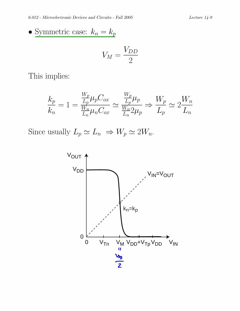
• Symmetric case: kn = kp
VM = VDD
2
This implies:
kp
kn = 1 =
Wp Lp
µpCox
Wn Ln
µnCox �
Wp Lp
µp
Wn Ln
2µp ⇒
Wp
Lp � 2
Wn
Ln
Since usually Lp � Ln ⇒ Wp � 2Wn.
VOUT
VIN=VOUT
0
VDD
kn=kp
VTn VM VDD+VTp VDD VIN 0
VV VV VV VVbetw
6.012 - Microelectronic Devices and Circuits - Fall 2005 Lecture 14-10
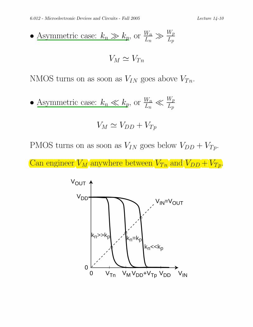
Wp• Asymmetric case: kn � kp, or Wn � LpLn
VM � VTn
NMOS turns on as soon as VIN goes above VTn.
Wp• Asymmetric case: kn � kp, or Wn � LpLn
VM � VDD + VTp
PMOS turns on as soon as VIN goes below VDD + VTp.
Can engineer VM anywhere een VTn and VDD + VTp.Can engineer VM anywhere between VTn and VDD + VTp.
VOUT
VIN=VOUT
0
VDD
kn>>kp kn=kp kn<<kp
0 VTn VM VDD+VTp VDD VIN
6.012 - Microelectronic Devices and Circuits - Fall 2005 Lecture 14-11
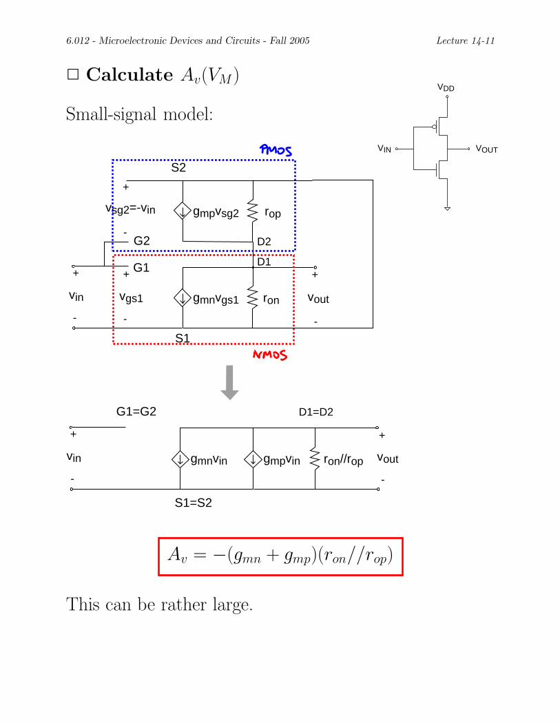
2 Calculate Av(VM ) VDD
Small-signal model:
VIN VOUT
G1
G1=G2
S1
D1
D1=D2
+
-
vin
+
-
vgs1
+
-
voutgmnvgs1 ron
+
-
vin voutgmnvin gmpvin ron//rop
G2
S2
D2
+
-
vsg2=-vin gmpvsg2 rop
+
-
S1=S2
Av = −(gmn + gmp)(ron//rop)
This can be rather large.
6.012 - Microelectronic Devices and Circuits - Fall 2005 Lecture 14-12
2 Noise margins
VOUT
VDD
VM
0
Av(VM)
NML
0 VILVM VIH VDD VIN
NMH
• Noise-margin-low:
VDD − VMVIL = VM − |Av|
Therefore:
VDD − VMNML = VIL − VOL = VIL = VM − |Av|
In the limit of |Av| → ∞:
NML → VM
6.012 - Microelectronic Devices and Circuits - Fall 2005 Lecture 14-13
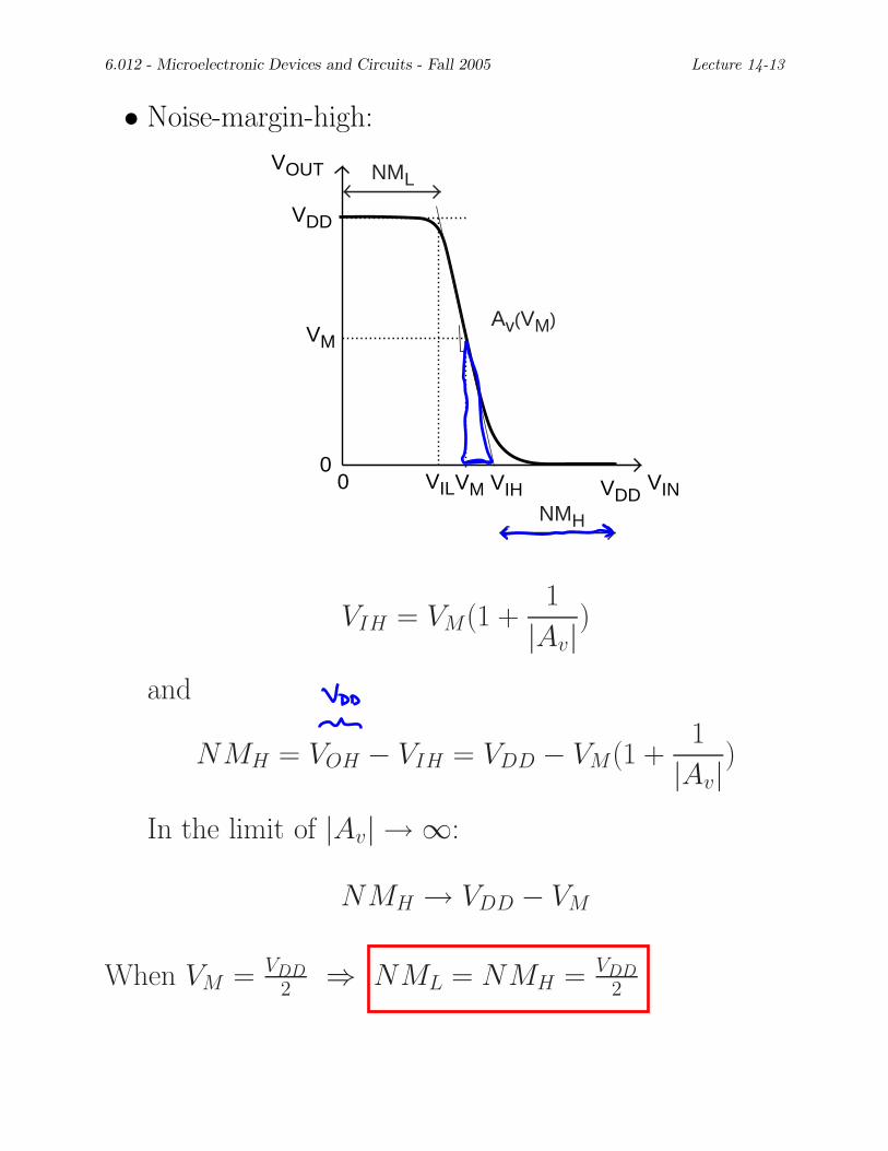
• Noise-margin-high:
VOUT
VDD
VM
0 0 VDD
VMVIL VIH
Av(VM)
NML
NMH
VIN
1 VIH = VM (1 + )|Av|
and
1 NMH = VOH − VIH = VDD − VM (1 + )|Av|
In the limit of |Av| → ∞:
NMH → VDD − VM
When VM = VDD ⇒ NML = NMH = VDD 2 2
6.012 - Microelectronic Devices and Circuits - Fall 2005 Lecture 14-14
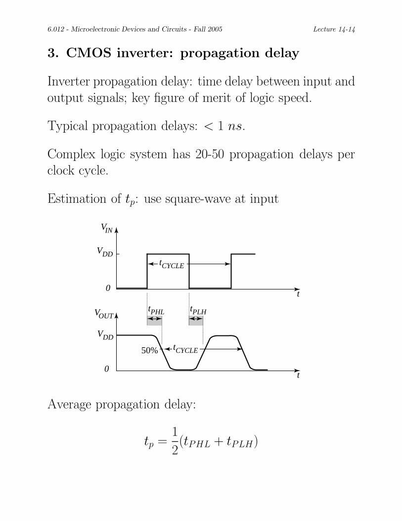
3. CMOS inverter: propagation delay
Inverter propagation delay: time delay between input and output signals; key figure of merit of logic speed.
Typical propagation delays: < 1 ns.
Complex logic system has 20-50 propagation delays perclock cycle.
Estimation of tp: use square-wave at input
VIN
VDD
0
VDD
VOUT tPHL tPLH
0
50%
t
t
tCYCLE
tCYCLE
Average propagation delay:
1 tp = (tPHL + tPLH )
2
6.012 - Microelectronic Devices and Circuits - Fall 2005 Lecture 14-15
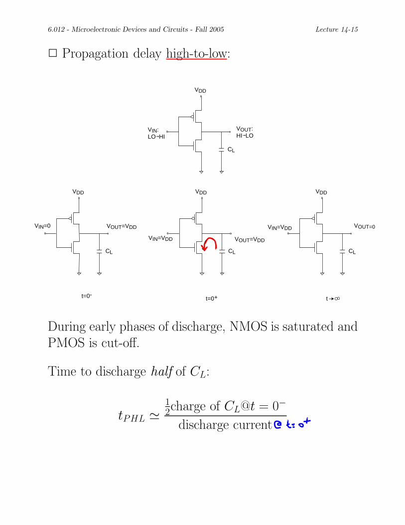
2 Propagation delay high-to-low:
VDD
VIN: VOUT: HI LO
CL
LO HI
VDD VDD VDD
VIN=0 VOUT=VDD
CL
VIN=VDD
VOUT=0VIN=VDD
12
VOUT=VDD
CL CL
t=0-t=0+ t
During early phases of discharge, NMOS is saturated and PMOS is cut-off.
Time to discharge half of CL:
charge of CL@t = 0−
tPHL � discharge current
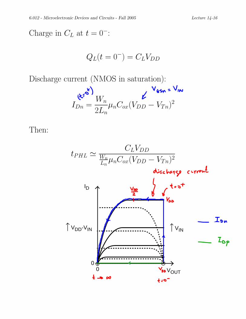
6.012 - Microelectronic Devices and Circuits - Fall 2005 Lecture 14-16
Charge in CL at t = 0−:
QL(t = 0−) = CLVDD
Discharge current (NMOS in saturation):
WnIDn = µnCox(VDD − VTn)2
2Ln
Then:
CLVDD tPHL � Wn µnCox(VDD − VTn)2
Ln
VOUT
VIN
0 0
VDD-VIN
ID
6.012 - Microelectronic Devices and Circuits - Fall 2005 Lecture 14-17
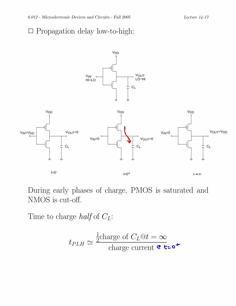
2 Propagation delay low-to-high:
VDD
VIN: HI LO
VOUT: LO HI
CL
VDD VDD VDD
VOUT=VDDVOUT=0 VIN=0VIN=VDD
V =0IN
12
VOUT=0
CL CL CL
t=0-t=0+ t
During early phases of charge, PMOS is saturated andNMOS is cut-off.
Time to charge half of CL:
charge of CL@t = ∞ tPLH �
charge current
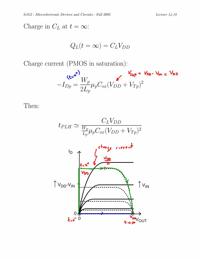
6.012 - Microelectronic Devices and Circuits - Fall 2005 Lecture 14-18
Charge in CL at t = ∞:
QL(t = ∞) = CLVDD
Charge current (PMOS in saturation):
Wp−IDp = µpCox(VDD + VTp)2
2Lp
Then:
CLVDD tPLH � Wp µpCox(VDD + VTp)2
Lp
VOUT
VIN
0 0
VDD-VIN
ID
6.012 - Microelectronic Devices and Circuits - Fall 2005 Lecture 14-19
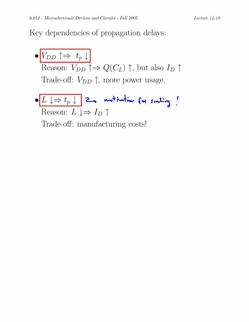
Key dependencies of propagation delays:
• VDD ↑⇒ tp ↓
Reason: VDD ↑⇒ Q(CL) ↑, but also ID ↑
Trade-off: VDD ↑, more power usage.
• L ↓⇒ tp ↓
Reason: L ↓⇒ ID ↑
Trade-off: manufacturing costs!
6.012 - Microelectronic Devices and Circuits - Fall 2005 Lecture 14-20
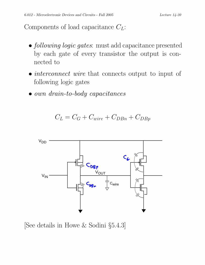
Components of load capacitance CL:
• following logic gates: must add capacitance presented by each gate of every transistor the output is con-nected to
• interconnect wire that connects output to input of following logic gates
• own drain-to-body capacitances
CL = CG + Cwire + CDBn + CDBp
VIN VOUT
Cwire
VDD
[See details in Howe & Sodini §5.4.3]
6.012 - Microelectronic Devices and Circuits - Fall 2005 Lecture 14-21
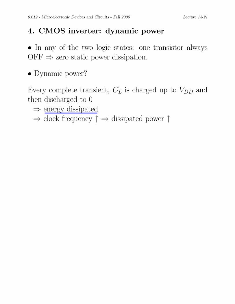
4. CMOS inverter: dynamic power
• In any of the two logic states: one transistor always OFF ⇒ zero static power dissipation.
• Dynamic power?
Every complete transient, CL is charged up to VDD and then discharged to 0 ⇒ energy dissipated⇒ clock frequency ↑ ⇒ dissipated power ↑
�
6.012 - Microelectronic Devices and Circuits - Fall 2005 Lecture 14-22
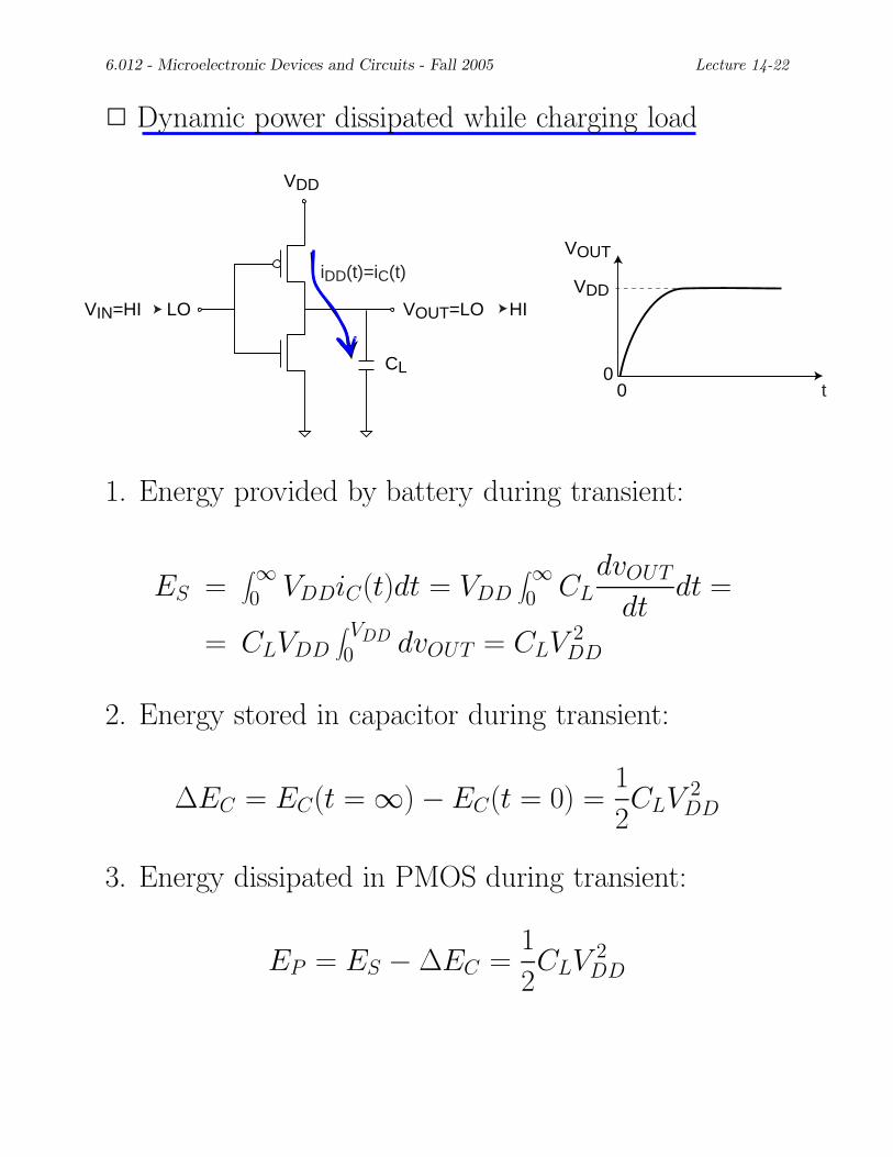
2 Dynamic power dissipated while charging load
VDD
VIN=HI LO VOUT=LO HI
VOUT
VDD
CL 0 0 t
iDD(t)=iC(t)
1. Energy provided by battery during transient:
� ∞ � ∞ dvOU T ES VDDiC (t)dt = VDD CL dt == 0 0 dt
VDD 0
2 DDCLVDD dvOU T = CLV=
2. Energy stored in capacitor during transient:
1 ∆EC = EC (t = ∞) − EC (t = 0) = CLV
2 2 DD
3. Energy dissipated in PMOS during transient:
1 EP = ES − ∆EC = CLV
2 2 DD
6.012 - Microelectronic Devices and Circuits - Fall 2005 Lecture 14-23
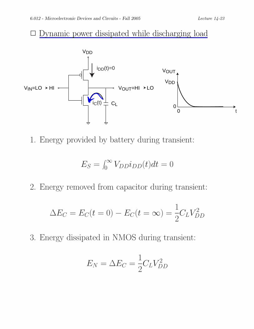
2 Dynamic power dissipated while discharging load
VDD
VIN=LO HI VOUT=HI LO
VOUT
VDD
CL 0 0 t
iC(t)
iDD(t)=0
1. Energy provided by battery during transient:
� ∞ES = 0 VDDiDD(t)dt = 0
2. Energy removed from capacitor during transient:
1 ∆EC = EC (t = 0) − EC (t = ∞) = CLV 2
2 DD
3. Energy dissipated in NMOS during transient:
1 EN = ∆EC = CLV 2
2 DD
undamental trade-off between switc eed ant owe
6.012 - Microelectronic Devices and Circuits - Fall 2005 Lecture 14-24
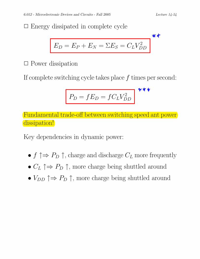
2 Energy dissipated in complete cycle
ED = EP + EN = ΣES = CLV 2 DD
2 Power dissipation
If complete switching cycle takes place f times per second:
PD = fED = fCLV 2 DD
F hing sp p r dissipation! Fundamental trade-off between switching speed ant powerdissipation!
Key dependencies in dynamic power:
• f ↑⇒ PD ↑, charge and discharge CL more frequently
• CL ↑⇒ PD ↑, more charge being shuttled around
• VDD ↑⇒ PD ↑, more charge being shuttled around
6.012 - Microelectronic Devices and Circuits - Fall 2005 Lecture 14-25
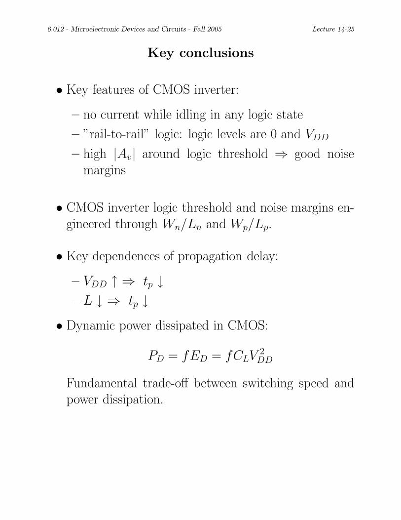
Key conclusions
• Key features of CMOS inverter:
– no current while idling in any logic state
– ”rail-to-rail” logic: logic levels are 0 and VDD
– high |Av| around logic threshold ⇒ good noise margins
• CMOS inverter logic threshold and noise margins en-gineered through Wn/Ln and Wp/Lp.
• Key dependences of propagation delay:
– VDD ↑ ⇒ tp ↓
– L ↓ ⇒ tp ↓
• Dynamic power dissipated in CMOS:
PD = fED = fCLV 2 DD
Fundamental trade-off between switching speed and power dissipation.