Embed Size (px)
Citation preview
© April 30, 2015, Dr. Lynn Fuller, Professor
CMOS Testing
Page 1
Rochester Institute of Technology
Microelectronic Engineering
ROCHESTER INSTITUTE OF TECHNOLOGY MICROELECTRONIC ENGINEERING
CMOS Testing for the Student Run Factory
Dr. Lynn Fuller Webpage: http://people.rit.edu/lffeee
Microelectronic Engineering Rochester Institute of Technology
82 Lomb Memorial Drive Rochester, NY 14623-5604
Tel (585) 475-2035 Email: [email protected]
Department webpage: http://www.microe.rit.edu
Revised 4-30-2015 cmostest.ppt
© April 30, 2015, Dr. Lynn Fuller, Professor
CMOS Testing
Page 2
Rochester Institute of Technology
Microelectronic Engineering
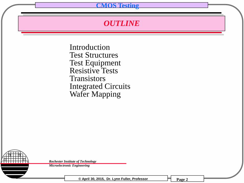
OUTLINE
Introduction Test Structures Test Equipment Resistive Tests Transistors Integrated Circuits Wafer Mapping
© April 30, 2015, Dr. Lynn Fuller, Professor
CMOS Testing
Page 3
Rochester Institute of Technology
Microelectronic Engineering
INTRODUCTION
Completed factory wafers are tested as part of the manufacturing process to capture data on processing parameters and transistor characteristics. Some simple integrated circuits are tested to verify functionality of more complex circuits. Uniformity is evaluated by measuring some parameters, such as threshold voltage, over the entire wafer. These tests are broken into four tasks that can be completed in our normal three hour laboratory time: 1. sheet resistance and contact resistance, 2. transistors, 3. inverters, ring oscillator and op amp, and 4. wafer map of NMOSFET threshold voltage. More complex digital and analog integrated circuits are tested outside of the factory by those who are interested.
© April 30, 2015, Dr. Lynn Fuller, Professor
CMOS Testing
Page 4
Rochester Institute of Technology
Microelectronic Engineering
INTRODUCTION
Chip designs always include test structures for the factory in addition to the specific integrated circuit or microsystem being fabricated. The test structures are often located along the edges of the chip and might even be removed after testing during the wafer sawing process. These test structures are available as cells that can be easily added to the integrated circuit or microsystem design. The test setups can be used for all completed chips. Automated probing (rarely done at RIT) may require different setups if the test structures are in different locations on the wafer. Three other documents provide additional details: CMOSTestchip2008.pdf - description of latest factory chip CMOSTEST_Manual.pdf –details for test equipment operation TestResults.pdf – recent factory test results and template for reporting test results
© April 30, 2015, Dr. Lynn Fuller, Professor
CMOS Testing
Page 5
Rochester Institute of Technology
Microelectronic Engineering
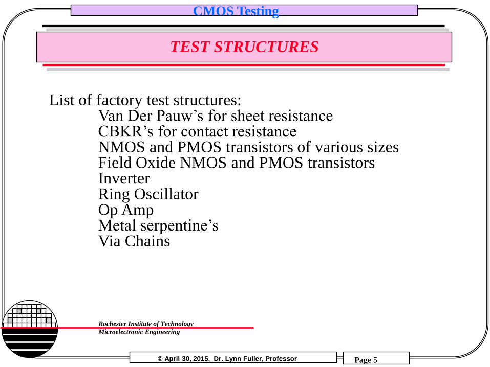
TEST STRUCTURES
List of factory test structures: Van Der Pauw’s for sheet resistance CBKR’s for contact resistance NMOS and PMOS transistors of various sizes Field Oxide NMOS and PMOS transistors Inverter Ring Oscillator Op Amp Metal serpentine’s Via Chains
© April 30, 2015, Dr. Lynn Fuller, Professor
CMOS Testing
Page 6
Rochester Institute of Technology
Microelectronic Engineering
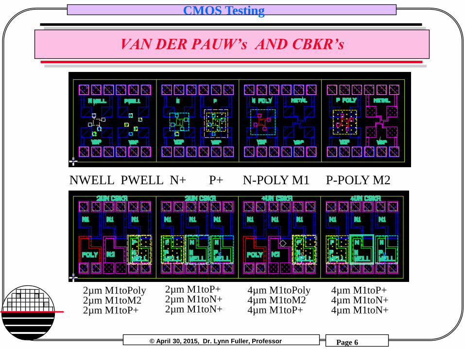
VAN DER PAUW’s AND CBKR’s
NWELL PWELL N+ P+ N-POLY M1 P-POLY M2
2µm M1toPoly 2µm M1toM2 2µm M1toP+
4µm M1toPoly 4µm M1toM2 4µm M1toP+
4µm M1toP+ 4µm M1toN+ 4µm M1toN+
2µm M1toP+ 2µm M1toN+ 2µm M1toN+
© April 30, 2015, Dr. Lynn Fuller, Professor
CMOS Testing
Page 7
Rochester Institute of Technology
Microelectronic Engineering
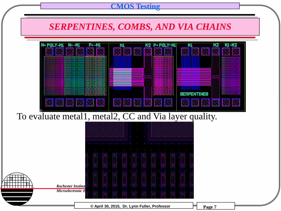
SERPENTINES, COMBS, AND VIA CHAINS
To evaluate metal1, metal2, CC and Via layer quality.
© April 30, 2015, Dr. Lynn Fuller, Professor
CMOS Testing
Page 8
Rochester Institute of Technology
Microelectronic Engineering
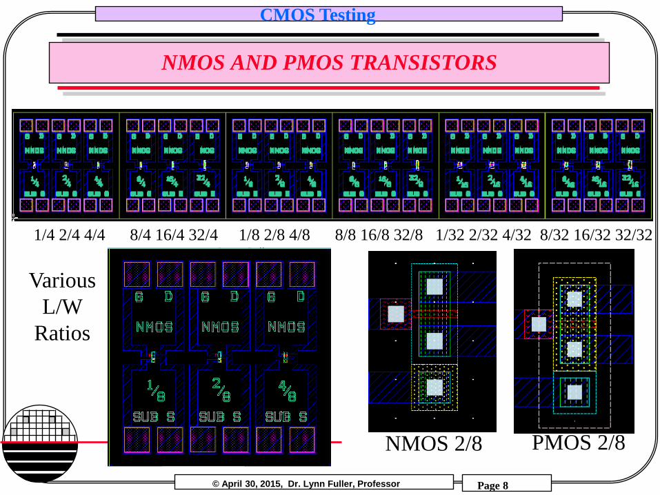
NMOS AND PMOS TRANSISTORS
Various
L/W
Ratios
PMOS 2/8
1/4 2/4 4/4 8/4 16/4 32/4 1/8 2/8 4/8 8/8 16/8 32/8 1/32 2/32 4/32 8/32 16/32 32/32
NMOS 2/8
© April 30, 2015, Dr. Lynn Fuller, Professor
CMOS Testing
Page 9
Rochester Institute of Technology
Microelectronic Engineering
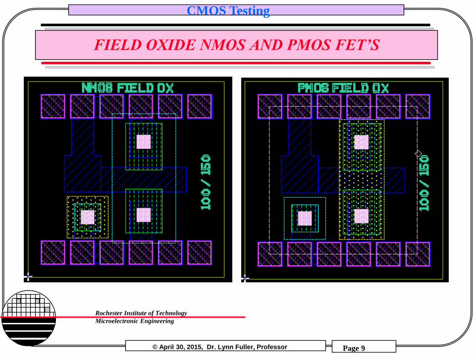
FIELD OXIDE NMOS AND PMOS FET’S
© April 30, 2015, Dr. Lynn Fuller, Professor
CMOS Testing
Page 10
Rochester Institute of Technology
Microelectronic Engineering
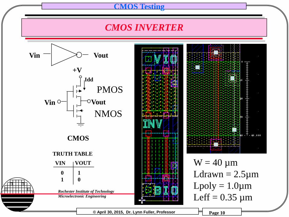
CMOS INVERTER
Vin Vout
Vin
CMOS
+V
Vout
Idd
TRUTH TABLE
VOUT VIN
0 1
1 0
PMOS
NMOS
W = 40 µm
Ldrawn = 2.5µm
Lpoly = 1.0µm
Leff = 0.35 µm
© April 30, 2015, Dr. Lynn Fuller, Professor
CMOS Testing
Page 11
Rochester Institute of Technology
Microelectronic Engineering
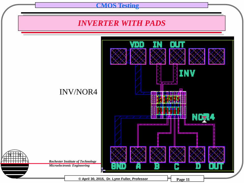
INVERTER WITH PADS
INV/NOR4
© April 30, 2015, Dr. Lynn Fuller, Professor
CMOS Testing
Page 12
Rochester Institute of Technology
Microelectronic Engineering
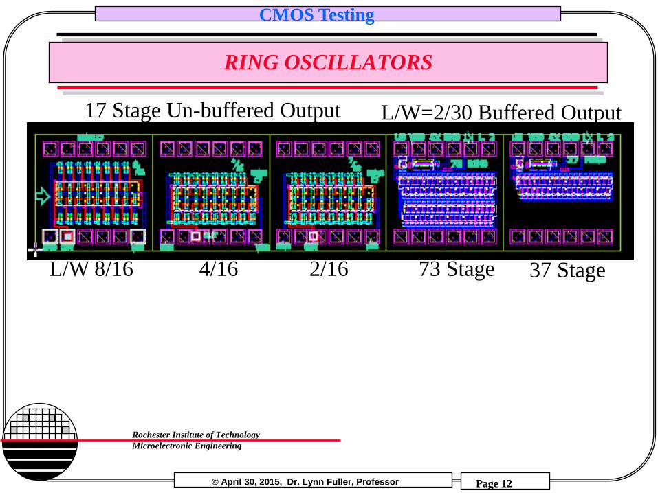
RING OSCILLATORS
17 Stage Un-buffered Output
L/W 8/16 4/16 2/16
L/W=2/30 Buffered Output
73 Stage 37 Stage
© April 30, 2015, Dr. Lynn Fuller, Professor
CMOS Testing
Page 13
Rochester Institute of Technology
Microelectronic Engineering
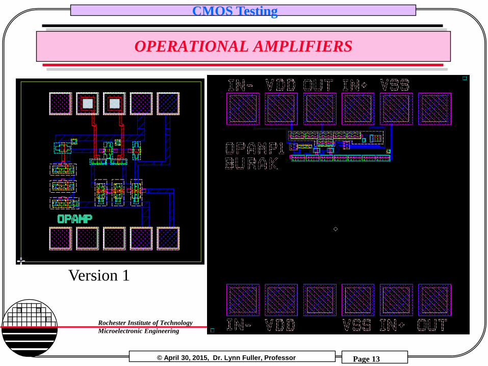
OPERATIONAL AMPLIFIERS
Version 1
© April 30, 2015, Dr. Lynn Fuller, Professor
CMOS Testing
Page 14
Rochester Institute of Technology
Microelectronic Engineering
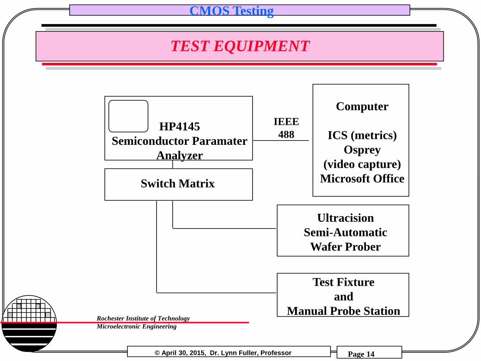
TEST EQUIPMENT
Switch Matrix
Ultracision
Semi-Automatic
Wafer Prober
HP4145
Semiconductor Paramater
Analyzer
Computer
ICS (metrics)
Osprey
(video capture)
Microsoft Office
Test Fixture
and
Manual Probe Station
IEEE
488
© April 30, 2015, Dr. Lynn Fuller, Professor
CMOS Testing
Page 15
Rochester Institute of Technology
Microelectronic Engineering
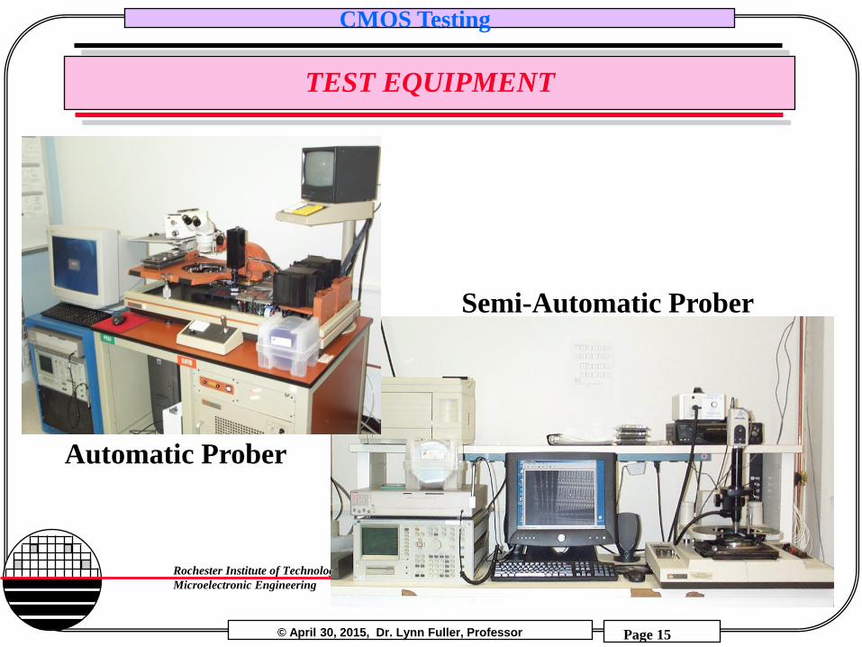
TEST EQUIPMENT
Automatic Prober
Semi-Automatic Prober
© April 30, 2015, Dr. Lynn Fuller, Professor
CMOS Testing
Page 16
Rochester Institute of Technology
Microelectronic Engineering
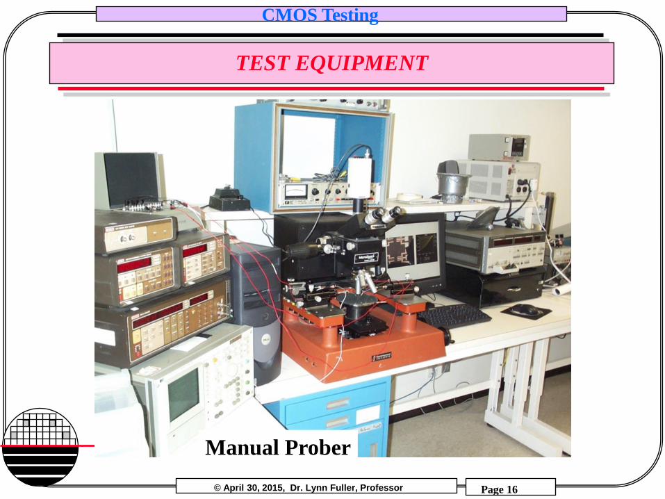
TEST EQUIPMENT
Manual Prober
© April 30, 2015, Dr. Lynn Fuller, Professor
CMOS Testing
Page 17
Rochester Institute of Technology
Microelectronic Engineering
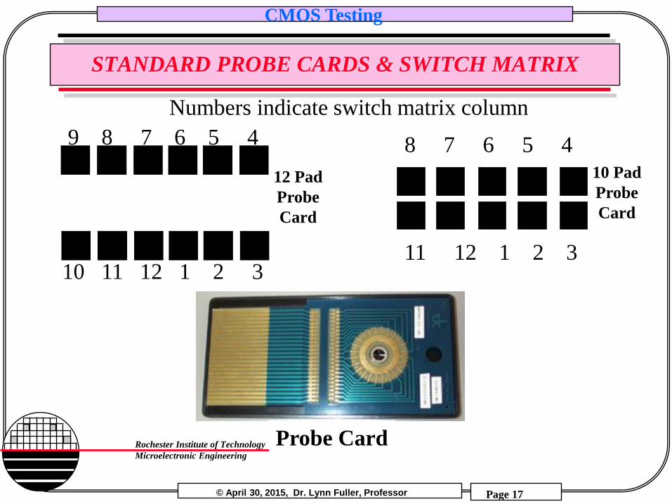
STANDARD PROBE CARDS & SWITCH MATRIX
Probe Card
8 7 6 5 4
11 12 1 2 3
10 Pad
Probe
Card
12 Pad
Probe
Card
Numbers indicate switch matrix column
9 8 7 6 5 4
10 11 12 1 2 3
© April 30, 2015, Dr. Lynn Fuller, Professor
CMOS Testing
Page 18
Rochester Institute of Technology
Microelectronic Engineering
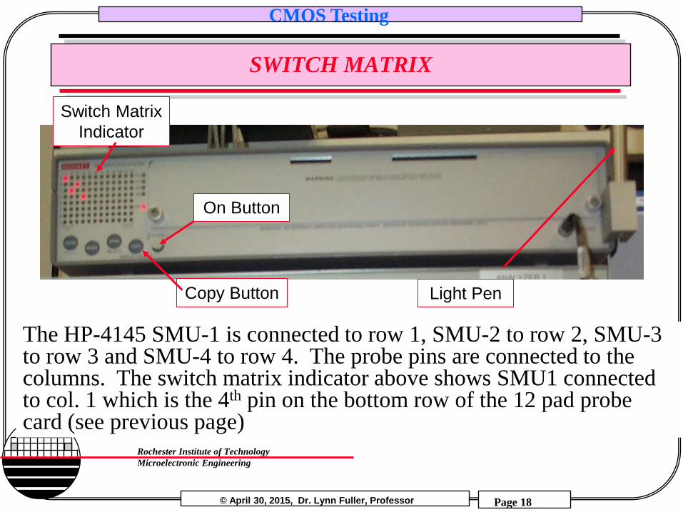
SWITCH MATRIX
Light Pen
On Button
Copy Button
Switch Matrix
Indicator
The HP-4145 SMU-1 is connected to row 1, SMU-2 to row 2, SMU-3 to row 3 and SMU-4 to row 4. The probe pins are connected to the columns. The switch matrix indicator above shows SMU1 connected to col. 1 which is the 4th pin on the bottom row of the 12 pad probe card (see previous page)
© April 30, 2015, Dr. Lynn Fuller, Professor
CMOS Testing
Page 19
Rochester Institute of Technology
Microelectronic Engineering
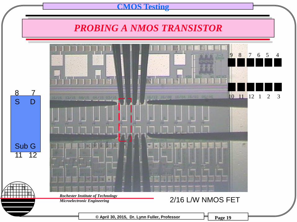
PROBING A NMOS TRANSISTOR
2/16 L/W NMOS FET
8 7
S D
Sub G
11 12
9 8 7 6 5 4
10 11 12 1 2 3
© April 30, 2015, Dr. Lynn Fuller, Professor
CMOS Testing
Page 20
Rochester Institute of Technology
Microelectronic Engineering
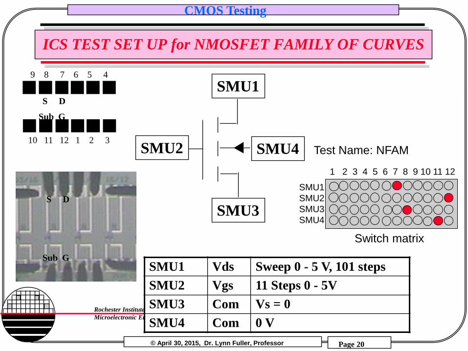
ICS TEST SET UP for NMOSFET FAMILY OF CURVES
SMU1 Vds Sweep 0 - 5 V, 101 steps
SMU2 Vgs 11 Steps 0 - 5V
SMU3 Com Vs = 0
SMU4 Com 0 V
SMU1
SMU3
SMU4
1 2 3 4 5 6 7 8 9 10 11 12
SMU1
SMU2
SMU3
SMU4
Test Name: NFAM
Switch matrix
S D
9 8 7 6 5 4
10 11 12 1 2 3
S D
Sub G
Sub G
SMU2
© April 30, 2015, Dr. Lynn Fuller, Professor
CMOS Testing
Page 21
Rochester Institute of Technology
Microelectronic Engineering
GENERAL TEST INSTRUCTIONS
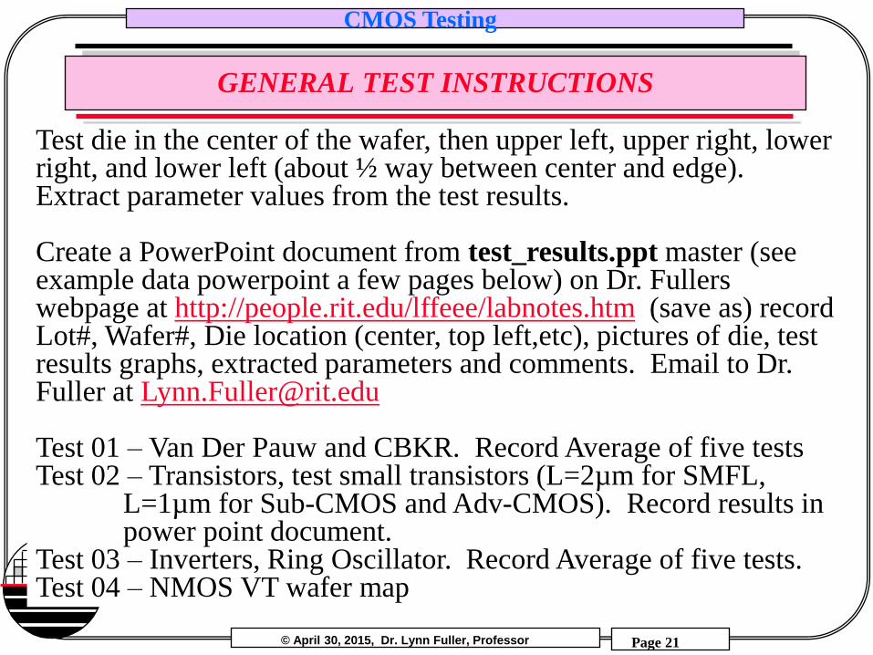
Test die in the center of the wafer, then upper left, upper right, lower right, and lower left (about ½ way between center and edge). Extract parameter values from the test results. Create a PowerPoint document from test_results.ppt master (see example data powerpoint a few pages below) on Dr. Fullers webpage at http://people.rit.edu/lffeee/labnotes.htm (save as) record Lot#, Wafer#, Die location (center, top left,etc), pictures of die, test results graphs, extracted parameters and comments. Email to Dr. Fuller at [email protected] Test 01 – Van Der Pauw and CBKR. Record Average of five tests Test 02 – Transistors, test small transistors (L=2µm for SMFL, L=1µm for Sub-CMOS and Adv-CMOS). Record results in power point document. Test 03 – Inverters, Ring Oscillator. Record Average of five tests. Test 04 – NMOS VT wafer map
© April 30, 2015, Dr. Lynn Fuller, Professor
CMOS Testing
Page 22
Rochester Institute of Technology
Microelectronic Engineering
GENERAL TEST INSTRUCTIONS
Substrate or Well Connections: Most of the test structures incorporate diffusions. In Resistors, Van der Pauw’s and Transistors the junctions between the diffusions and the substrate/wells are normally never forward biased. As a result the test engineer needs to evaluate the applied test voltages and connections to the substrate/wells and connections to the diffusions to ensure proper bias conditions. For example: a P+ Van der Pauw in an N-type Well requires that the Well connection always have the highest positive voltage that is applied. If a separate (5th pad) connection is available (not often because there are only 4 SMU’s) that can be set to a high voltage. Otherwise the substrate is normally connected to one of the four pads of the Van der Pauw. This pad can be swept with positive voltage thus keeping the substrate/well junction reverse biased.
© April 30, 2015, Dr. Lynn Fuller, Professor
CMOS Testing
Page 23
Rochester Institute of Technology
Microelectronic Engineering
GENERAL TEST INSTRUCTIONS
Each test requires you to: 1. Find the structure you want to test 2. Place the probes 3. Open the test by restoring the “testname”-1 (example PFAM-1) in
ICS, view the test setup to see what SMU’s do what. 4. Set the switch matrix for the HP4145 SMU’s to the probes you are
using, consistent with the test setup. 5. Edit the graph by making changes in the title, moving the cursors
to the correct location 6. Copy the plot using ctrl print screen, (paste into word, copy from
word to power point, crop and paste in correct location) 7. Extract the data, such as threshold voltage or LAMBDA and enter
the value in the data table in the powerpoint 8. Save the powerpoint, minimize the data plot on ICS 9. When done email the powerpoint to [email protected]
© April 30, 2015, Dr. Lynn Fuller, Professor
CMOS Testing
Page 24
Rochester Institute of Technology
Microelectronic Engineering
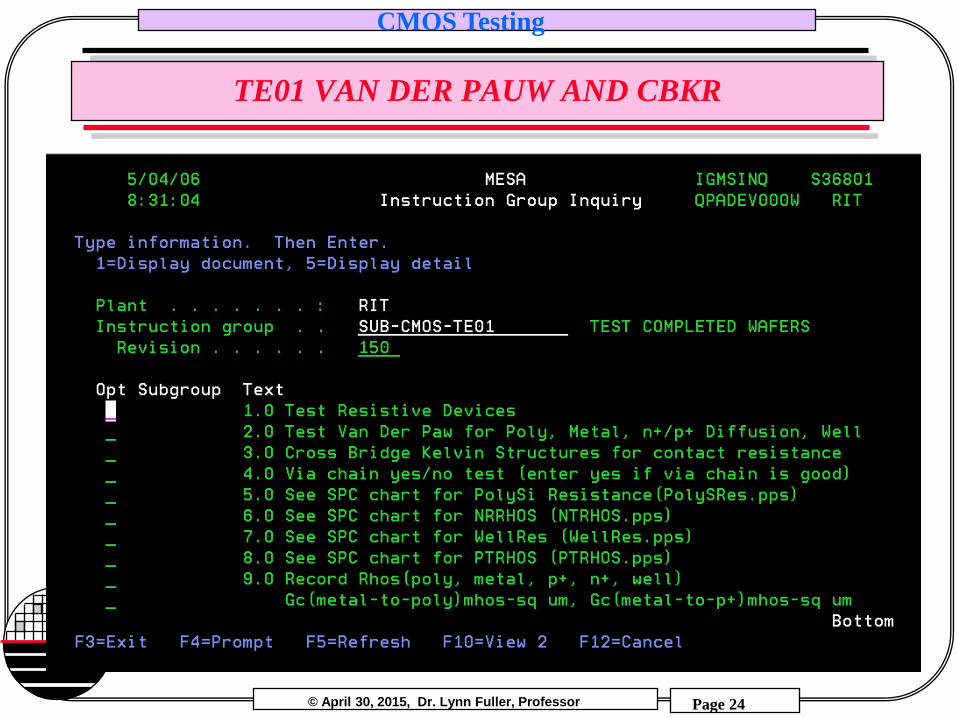
TE01 VAN DER PAUW AND CBKR
© April 30, 2015, Dr. Lynn Fuller, Professor
CMOS Testing
Page 25
Rochester Institute of Technology
Microelectronic Engineering
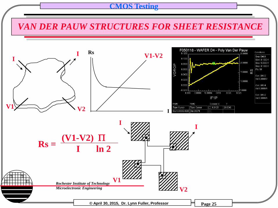
VAN DER PAUW STRUCTURES FOR SHEET RESISTANCE
I
I
V2 V1
(V1-V2)
I ln 2 Rs =
Rs
I
I
V2
V1
I V1-V2
© April 30, 2015, Dr. Lynn Fuller, Professor
CMOS Testing
Page 26
Rochester Institute of Technology
Microelectronic Engineering
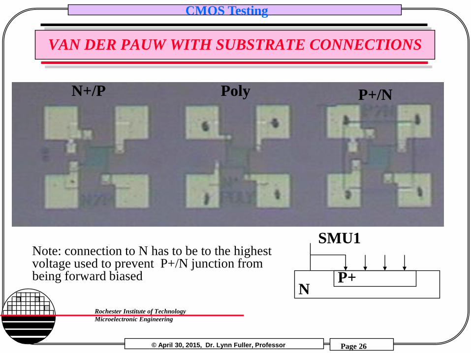
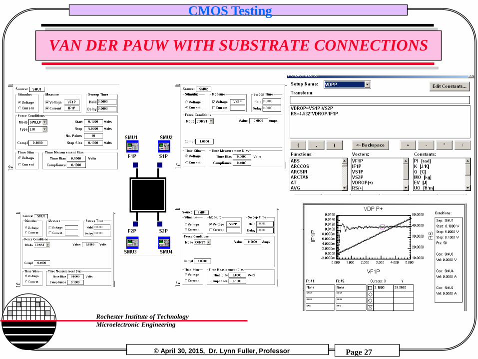
VAN DER PAUW WITH SUBSTRATE CONNECTIONS
P+/N Poly N+/P
P+ N
SMU1 Note: connection to N has to be to the highest voltage used to prevent P+/N junction from being forward biased
© April 30, 2015, Dr. Lynn Fuller, Professor
CMOS Testing
Page 27
Rochester Institute of Technology
Microelectronic Engineering
VAN DER PAUW WITH SUBSTRATE CONNECTIONS
© April 30, 2015, Dr. Lynn Fuller, Professor
CMOS Testing
Page 28
Rochester Institute of Technology
Microelectronic Engineering
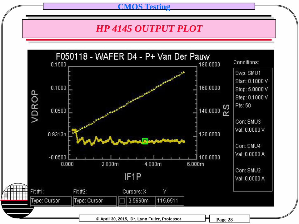
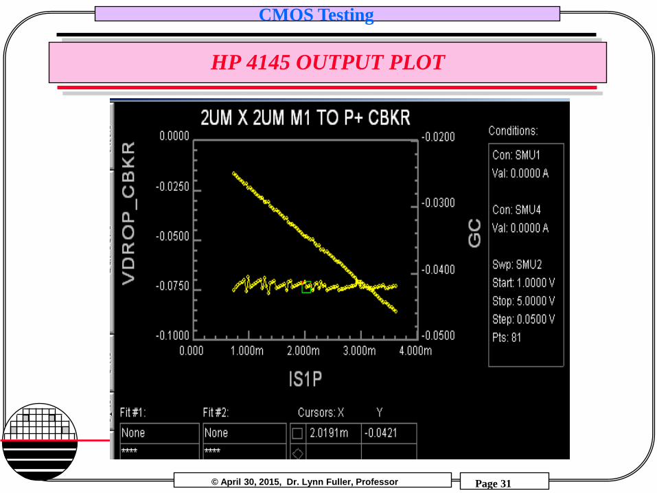
HP 4145 OUTPUT PLOT
© April 30, 2015, Dr. Lynn Fuller, Professor
CMOS Testing
Page 29
Rochester Institute of Technology
Microelectronic Engineering
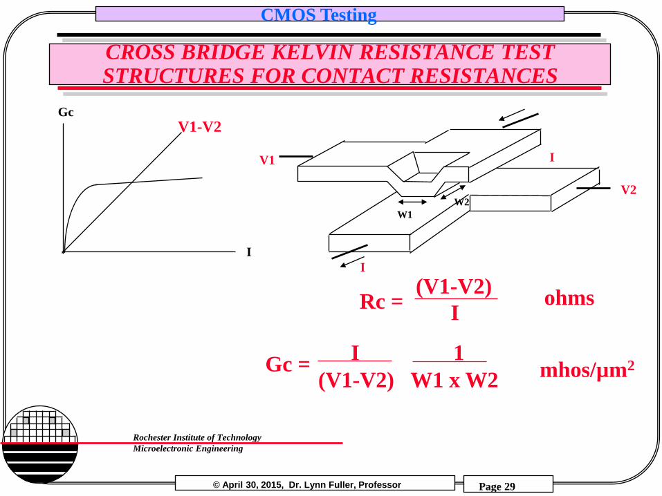
CROSS BRIDGE KELVIN RESISTANCE TEST STRUCTURES FOR CONTACT RESISTANCES
W2
W1
I
I
V2
V1
(V1-V2)
I Rc =
(V1-V2) W1 x W2
I 1 Gc =
ohms
mhos/µm2
Gc
I
V1-V2
© April 30, 2015, Dr. Lynn Fuller, Professor
CMOS Testing
Page 30
Rochester Institute of Technology
Microelectronic Engineering
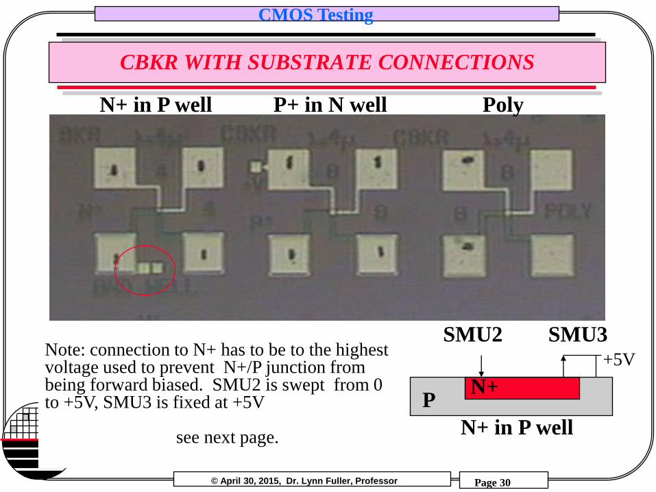
CBKR WITH SUBSTRATE CONNECTIONS
N+ in P well P+ in N well Poly
N+ P
SMU2 Note: connection to N+ has to be to the highest voltage used to prevent N+/P junction from being forward biased. SMU2 is swept from 0 to +5V, SMU3 is fixed at +5V see next page.
SMU3
N+ in P well
+5V
© April 30, 2015, Dr. Lynn Fuller, Professor
CMOS Testing
Page 31
Rochester Institute of Technology
Microelectronic Engineering
HP 4145 OUTPUT PLOT
© April 30, 2015, Dr. Lynn Fuller, Professor
CMOS Testing
Page 32
Rochester Institute of Technology
Microelectronic Engineering
TE02 TRANSISTORS
© April 30, 2015, Dr. Lynn Fuller, Professor
CMOS Testing
Page 33
Rochester Institute of Technology
Microelectronic Engineering
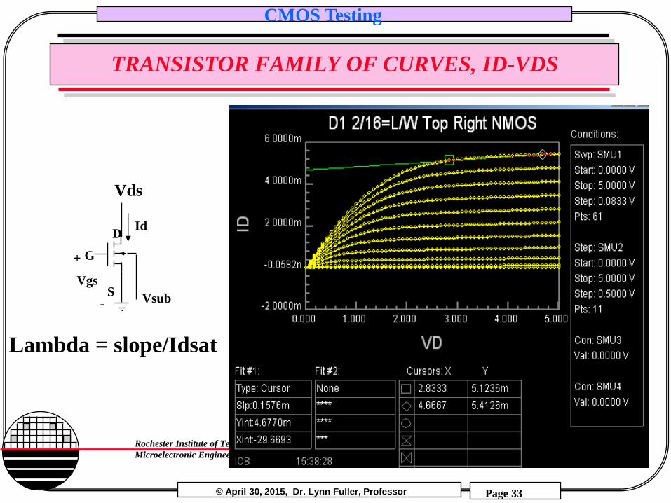
TRANSISTOR FAMILY OF CURVES, ID-VDS
G
D
S Vgs
Id
+
- Vsub
Vds
Lambda = slope/Idsat
© April 30, 2015, Dr. Lynn Fuller, Professor
CMOS Testing
Page 34
Rochester Institute of Technology
Microelectronic Engineering
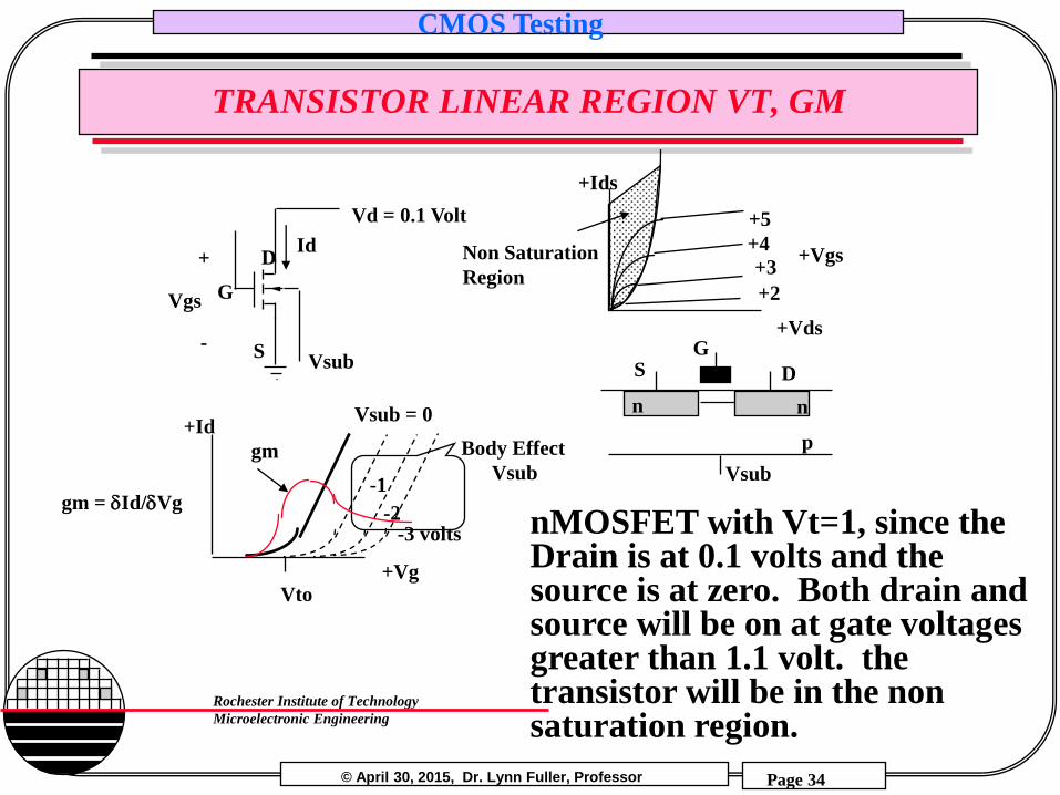
TRANSISTOR LINEAR REGION VT, GM
nMOSFET with Vt=1, since the Drain is at 0.1 volts and the source is at zero. Both drain and source will be on at gate voltages greater than 1.1 volt. the transistor will be in the non saturation region.
Vsub
n n
S G
D
p
+Vg
+Id
Vto
Vsub = 0
-2
-1
-3 volts
Body Effect
Vsub
G
D
S
Vgs
Id +
- Vsub
Vd = 0.1 Volt
+Ids
+Vgs
+Vds
+5
+4
+3
+2
Non Saturation
Region
gm
gm = Id/Vg
© April 30, 2015, Dr. Lynn Fuller, Professor
CMOS Testing
Page 35
Rochester Institute of Technology
Microelectronic Engineering
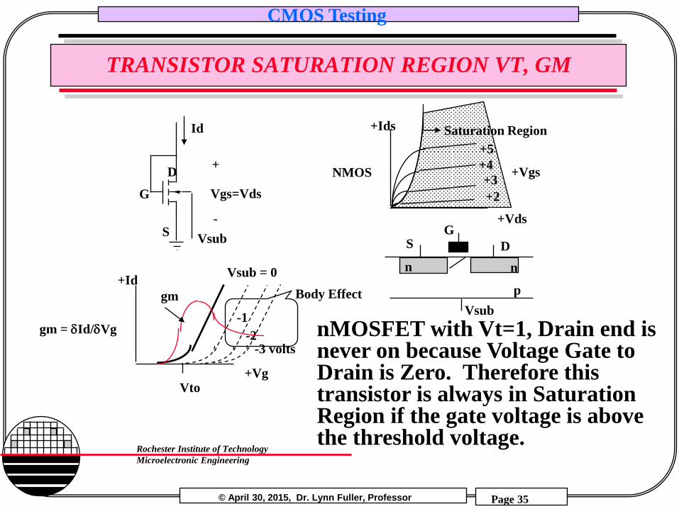
TRANSISTOR SATURATION REGION VT, GM
+Ids
+Vgs
+Vds
NMOS
+5
+4
+3
+2
Saturation Region
nMOSFET with Vt=1, Drain end is never on because Voltage Gate to Drain is Zero. Therefore this transistor is always in Saturation Region if the gate voltage is above the threshold voltage.
G
D
S
Vgs=Vds
Id
+
-
Vsub
Vsub
n n
S G
D
p
+Vg
+Id
Vto
Vsub = 0
-2
-1
-3 volts
Body Effect gm
gm = Id/Vg
© April 30, 2015, Dr. Lynn Fuller, Professor
CMOS Testing
Page 36
Rochester Institute of Technology
Microelectronic Engineering
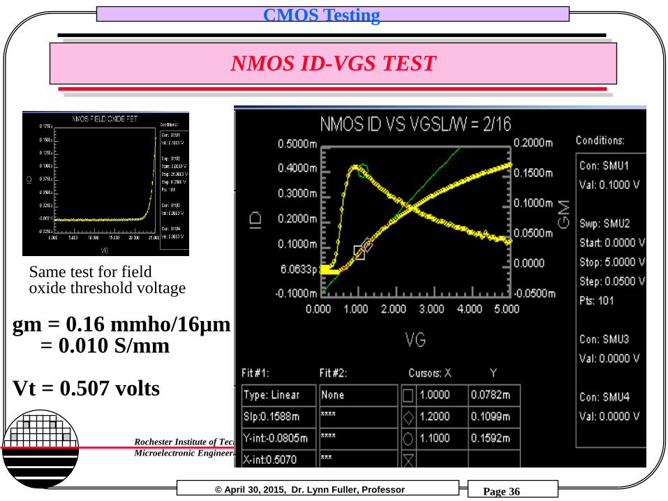
NMOS ID-VGS TEST
Same test for field oxide threshold voltage
gm = 0.16 mmho/16µm = 0.010 S/mm Vt = 0.507 volts
© April 30, 2015, Dr. Lynn Fuller, Professor
CMOS Testing
Page 37
Rochester Institute of Technology
Microelectronic Engineering
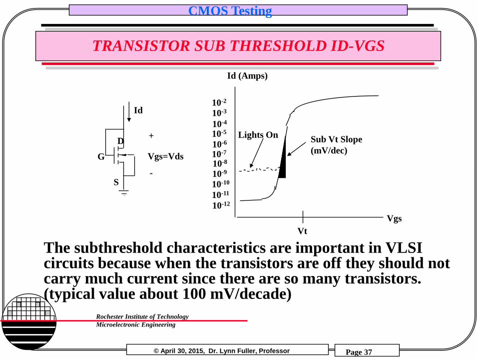
TRANSISTOR SUB THRESHOLD ID-VGS
Id (Amps)
10-5
Vgs
Vt
Sub Vt Slope
(mV/dec)
10-4
10-3
10-2
10-10
10-9
10-8 10-7
10-6
10-11
10-12
The subthreshold characteristics are important in VLSI circuits because when the transistors are off they should not carry much current since there are so many transistors. (typical value about 100 mV/decade)
Lights On
G
D
S
Vgs=Vds
Id
+
-
© April 30, 2015, Dr. Lynn Fuller, Professor
CMOS Testing
Page 38
Rochester Institute of Technology
Microelectronic Engineering
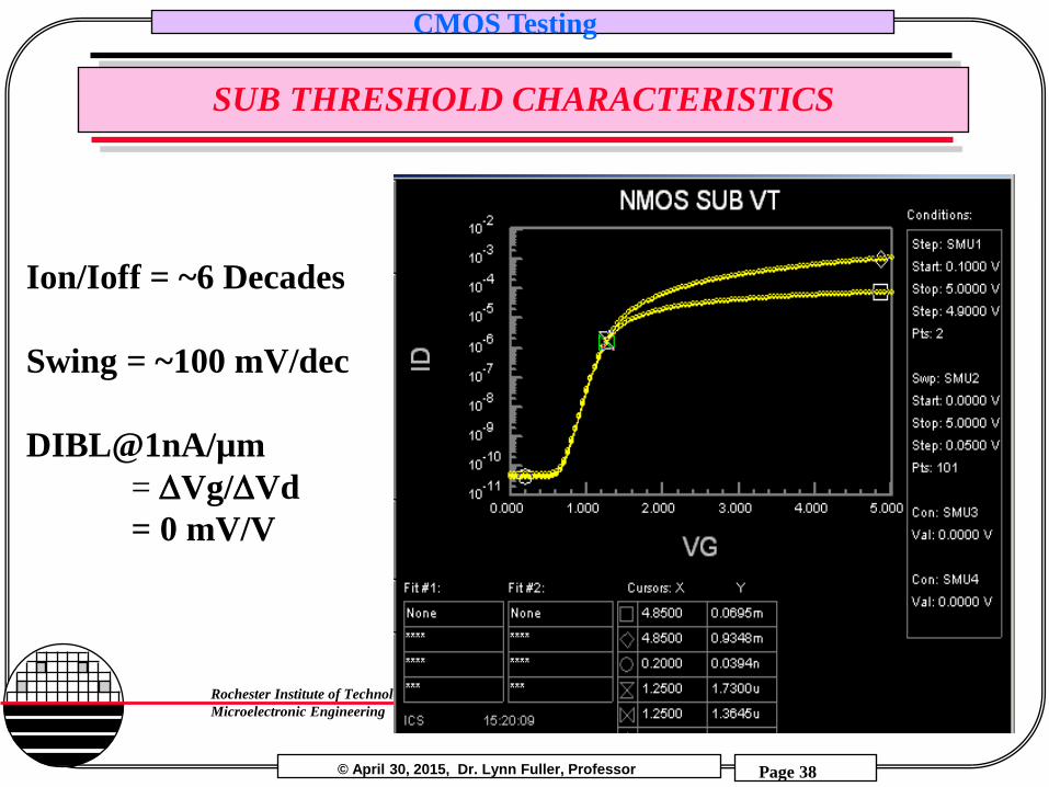
SUB THRESHOLD CHARACTERISTICS
Ion/Ioff = ~6 Decades
Swing = ~100 mV/dec
DIBL@1nA/µm
= Vg/Vd
= 0 mV/V
© April 30, 2015, Dr. Lynn Fuller, Professor
CMOS Testing
Page 39
Rochester Institute of Technology
Microelectronic Engineering
TE03 INTEGRATED CIRCUITS
© April 30, 2015, Dr. Lynn Fuller, Professor
CMOS Testing
Page 40
Rochester Institute of Technology
Microelectronic Engineering
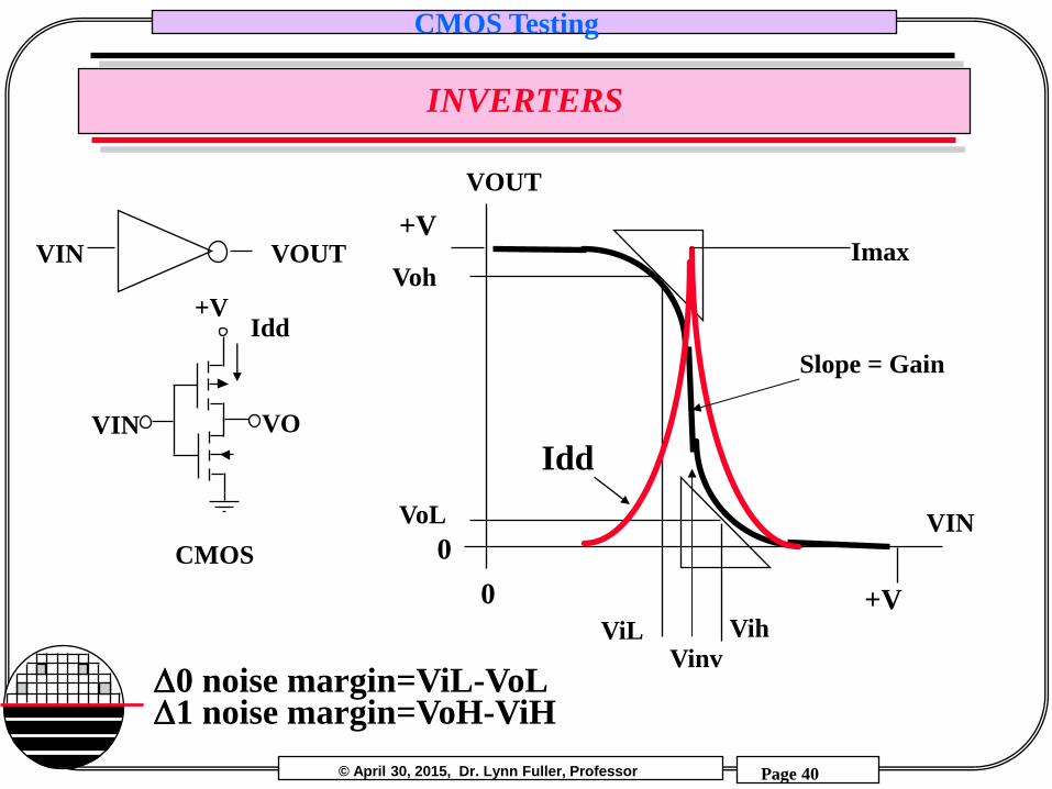
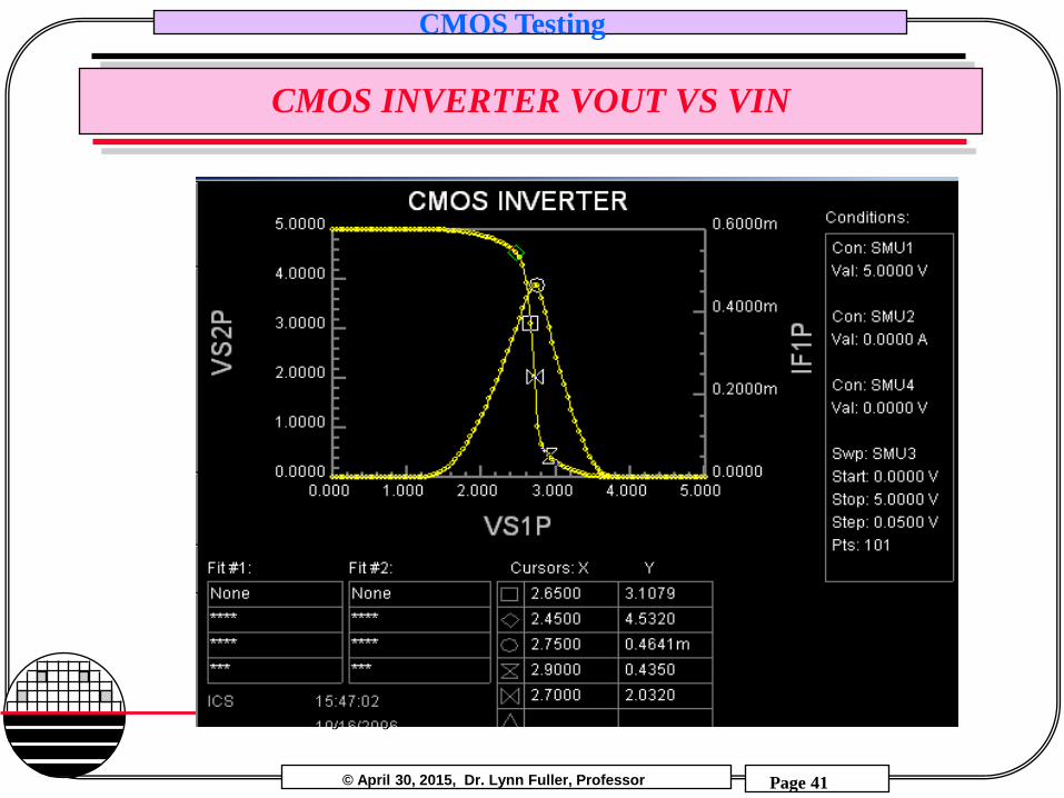
INVERTERS
VIN VOUT
VIN
CMOS
+V
VO
Idd
+V 0
0
+V
ViL
Voh
VoL
Vih
Imax
VOUT
VIN
Idd
0 noise margin=ViL-VoL 1 noise margin=VoH-ViH
Slope = Gain
Vinv
© April 30, 2015, Dr. Lynn Fuller, Professor
CMOS Testing
Page 41
Rochester Institute of Technology
Microelectronic Engineering
CMOS INVERTER VOUT VS VIN
© April 30, 2015, Dr. Lynn Fuller, Professor
CMOS Testing
Page 42
Rochester Institute of Technology
Microelectronic Engineering
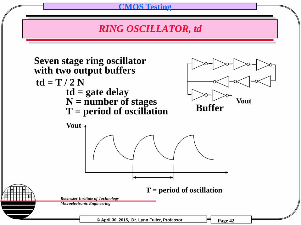
RING OSCILLATOR, td
td = T / 2 N td = gate delay N = number of stages T = period of oscillation
Vout
Seven stage ring oscillator with two output buffers
T = period of oscillation
Vout
Buffer
© April 30, 2015, Dr. Lynn Fuller, Professor
CMOS Testing
Page 43
Rochester Institute of Technology
Microelectronic Engineering
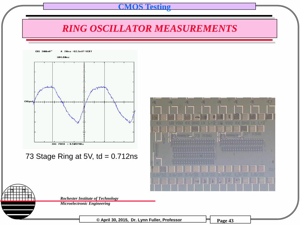
RING OSCILLATOR MEASUREMENTS
73 Stage Ring at 5V, td = 0.712ns
© April 30, 2015, Dr. Lynn Fuller, Professor
CMOS Testing
Page 44
Rochester Institute of Technology
Microelectronic Engineering
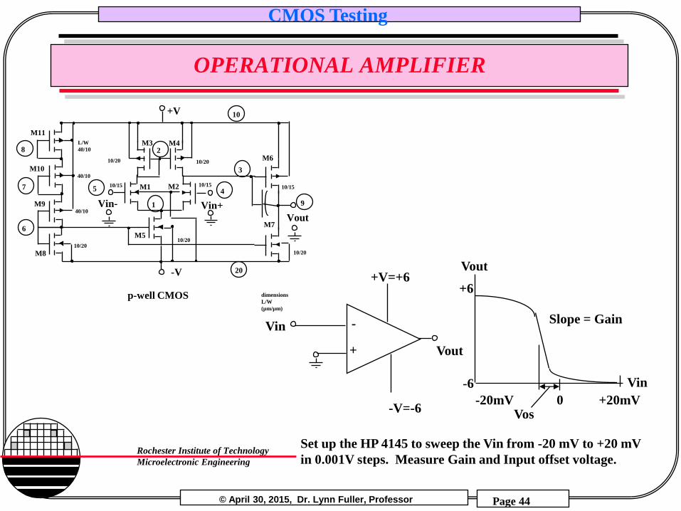
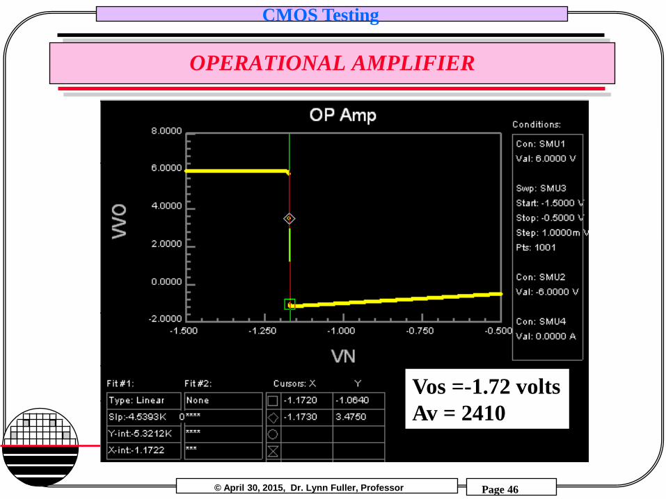
OPERATIONAL AMPLIFIER
+V
-V
Vin+
Vout
Vin-
M1 M2
M3
M5
M4
M7
M6
M8
M9
M10
M11
40/10
40/10
L/W
40/10
10/20
10/15
10/20 10/20
10/20
10/20
10/15 10/15
dimensions
L/W
(µm/µm)
p-well CMOS
8
7
6
5
1
2
3
9
4
20
10
Vout
+V=+6
-V=-6
Vin
+
-
Vin
-20mV +20mV 0 Vos
Slope = Gain
Vout
-6
+6
Set up the HP 4145 to sweep the Vin from -20 mV to +20 mV
in 0.001V steps. Measure Gain and Input offset voltage.
© April 30, 2015, Dr. Lynn Fuller, Professor
CMOS Testing
Page 45
Rochester Institute of Technology
Microelectronic Engineering
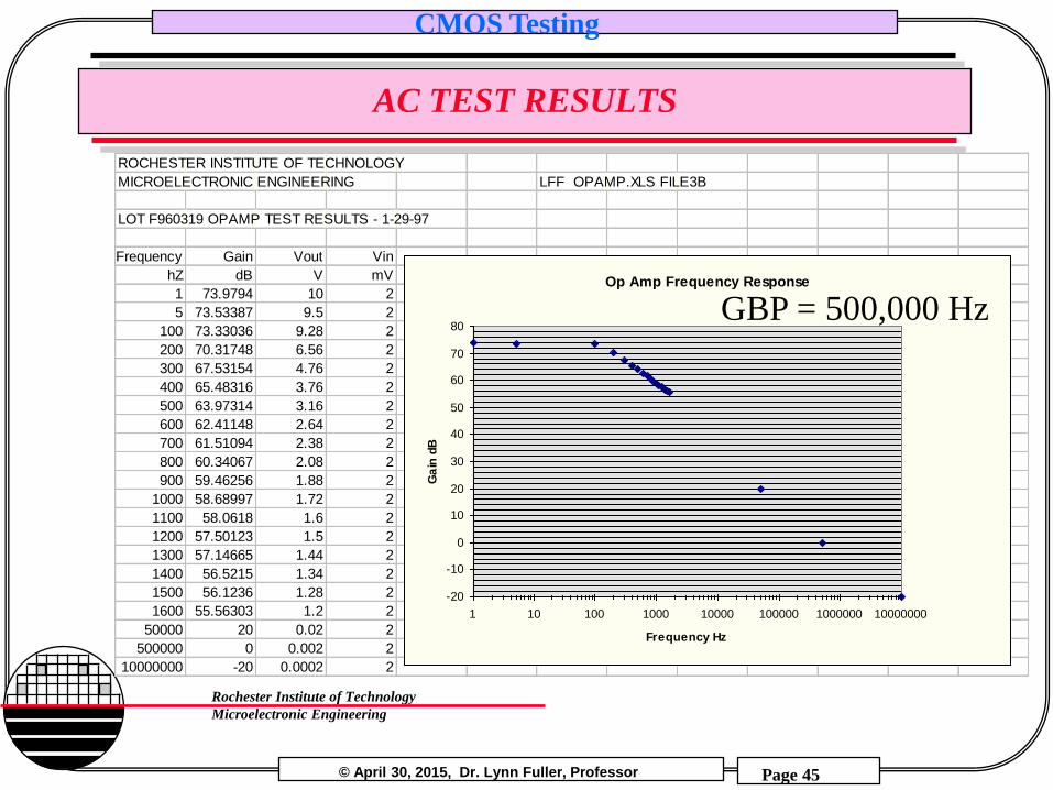
AC TEST RESULTS
ROCHESTER INSTITUTE OF TECHNOLOGY
MICROELECTRONIC ENGINEERING LFF OPAMP.XLS FILE3B
LOT F960319 OPAMP TEST RESULTS - 1-29-97
Frequency Gain Vout Vin
hZ dB V mV
1 73.9794 10 2
5 73.53387 9.5 2
100 73.33036 9.28 2
200 70.31748 6.56 2
300 67.53154 4.76 2
400 65.48316 3.76 2
500 63.97314 3.16 2
600 62.41148 2.64 2
700 61.51094 2.38 2
800 60.34067 2.08 2
900 59.46256 1.88 2
1000 58.68997 1.72 2
1100 58.0618 1.6 2
1200 57.50123 1.5 2
1300 57.14665 1.44 2
1400 56.5215 1.34 2
1500 56.1236 1.28 2
1600 55.56303 1.2 2
50000 20 0.02 2
500000 0 0.002 2
10000000 -20 0.0002 2
Op Amp Frequency Response
-20
-10
0
10
20
30
40
50
60
70
80
1 10 100 1000 10000 100000 1000000 10000000
Frequency Hz
Ga
in d
B
GBP = 500,000 Hz
© April 30, 2015, Dr. Lynn Fuller, Professor
CMOS Testing
Page 46
Rochester Institute of Technology
Microelectronic Engineering
OPERATIONAL AMPLIFIER
Vos =-1.72 volts
Av = 2410
© April 30, 2015, Dr. Lynn Fuller, Professor
CMOS Testing
Page 47
Rochester Institute of Technology
Microelectronic Engineering
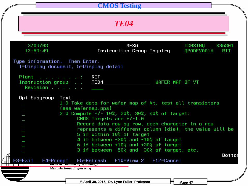
TE04
© April 30, 2015, Dr. Lynn Fuller, Professor
CMOS Testing
Page 48
Rochester Institute of Technology
Microelectronic Engineering
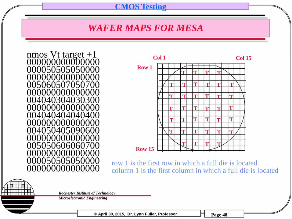
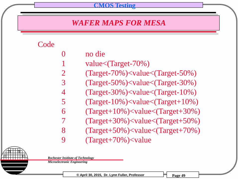
WAFER MAPS FOR MESA
T
T T
T
T T
T
T
T T
T T
T
T
T
T
T
T
T
T
T
T
T
T
T
T
T
T
T
T T
T T
T T
T
T
T
Row 1
Row 15
Col 15 Col 1 nmos Vt target +1 000000000000000 000050505050000 000000000000000 005060507050700 000000000000000 004040304030300 000000000000000 004040404040400 000000000000000 004050405090600 000000000000000 005050606060700 000000000000000 000050505050000 000000000000000
row 1 is the first row in which a full die is located column 1 is the first column in which a full die is located
© April 30, 2015, Dr. Lynn Fuller, Professor
CMOS Testing
Page 49
Rochester Institute of Technology
Microelectronic Engineering
WAFER MAPS FOR MESA
Code
0 no die
1 value<(Target-70%)
2 (Target-70%)<value<(Target-50%)
3 (Target-50%)<value<(Target-30%)
4 (Target-30%)<value<(Target-10%)
5 (Target-10%)<value<(Target+10%)
6 (Target+10%)<value<(Target+30%)
7 (Target+30%)<value<(Target+50%)
8 (Target+50%)<value<(Target+70%)
9 (Target+70%)<value
© April 30, 2015, Dr. Lynn Fuller, Professor
CMOS Testing
Page 50
Rochester Institute of Technology
Microelectronic Engineering
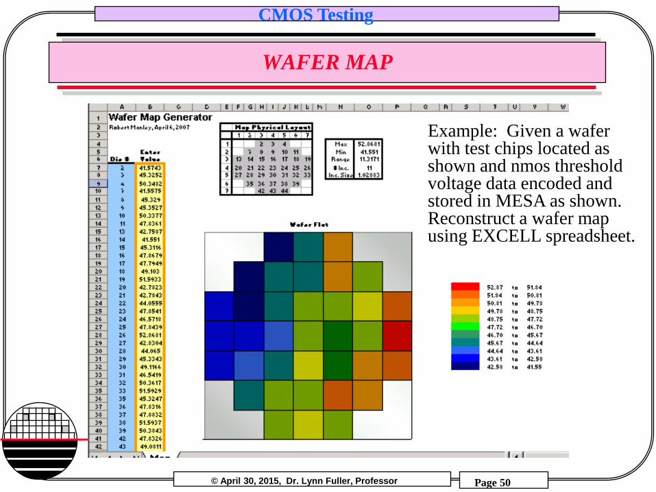
WAFER MAP
Example: Given a wafer with test chips located as shown and nmos threshold voltage data encoded and stored in MESA as shown. Reconstruct a wafer map using EXCELL spreadsheet.
PMOS Id-Vds Family of Curves
PMOS Id-Vgs
PMOS Subthreshold Characteristics
PMOS Field VT
NMOS Id-Vds Family of Curves
NMOS Id-Vgs
NMOS Subthreshold Characteristics
NMOS Field VT
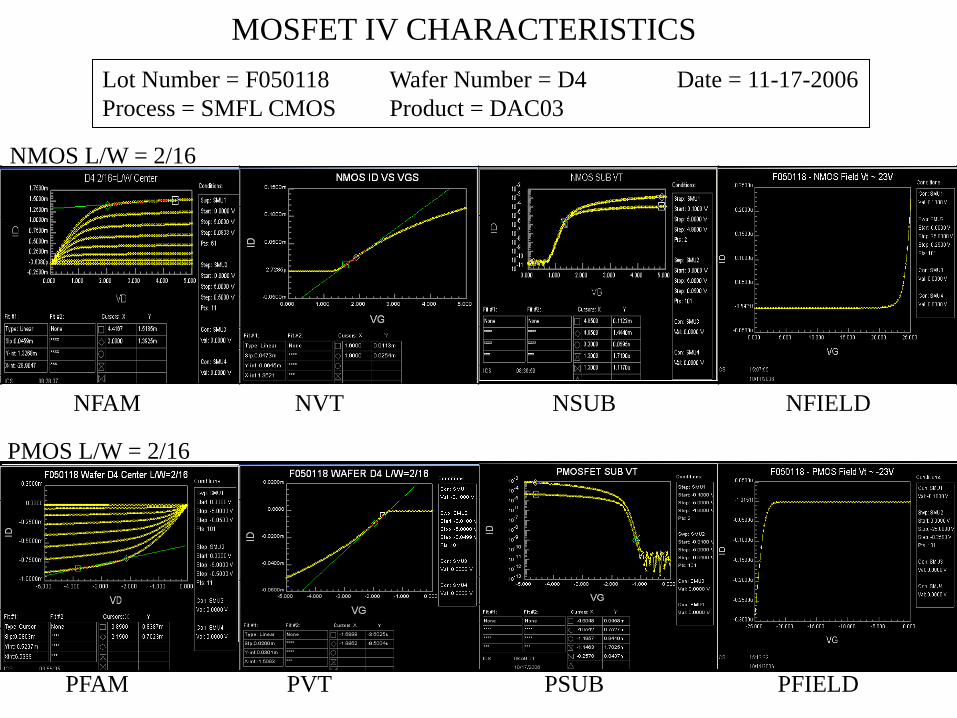
MOSFET IV CHARACTERISTICS
Lot Number = F050118 Wafer Number = D4 Date = 11-17-2006
Process = SMFL CMOS Product = DAC03
NFAM NVT NSUB NFIELD
PFAM PVT PSUB PFIELD
NMOS L/W = 2/16
PMOS L/W = 2/16
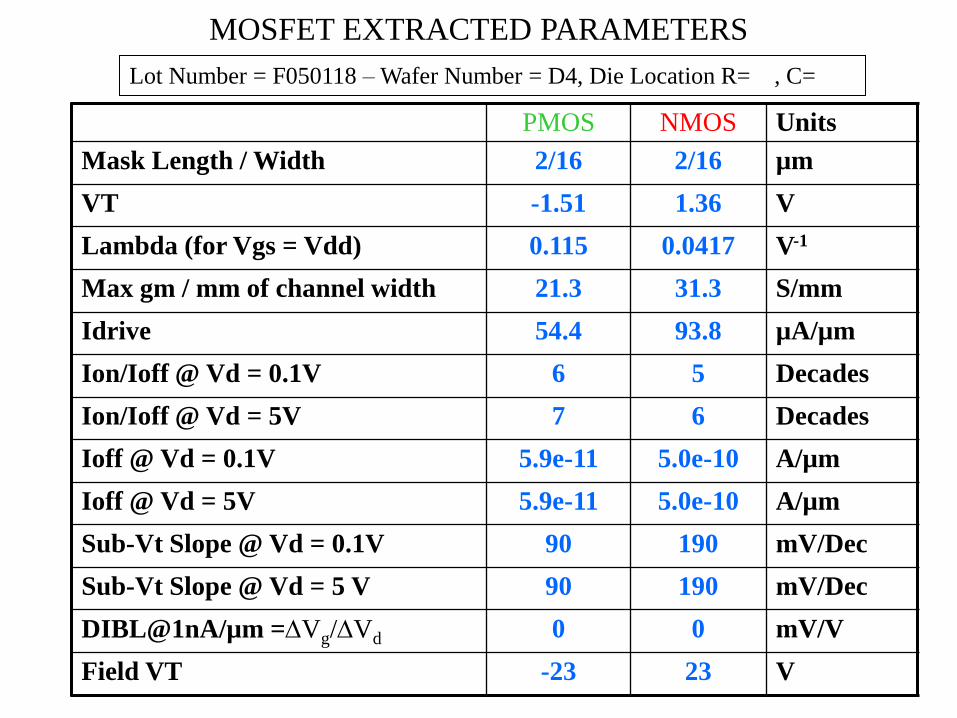
PMOS NMOS Units
Mask Length / Width 2/16 2/16 µm
VT -1.51 1.36 V
Lambda (for Vgs = Vdd) 0.115 0.0417 V-1
Max gm / mm of channel width 21.3 31.3 S/mm
Idrive 54.4 93.8 µA/µm
Ion/Ioff @ Vd = 0.1V 6 5 Decades
Ion/Ioff @ Vd = 5V 7 6 Decades
Ioff @ Vd = 0.1V 5.9e-11 5.0e-10 A/µm
Ioff @ Vd = 5V 5.9e-11 5.0e-10 A/µm
Sub-Vt Slope @ Vd = 0.1V 90 190 mV/Dec
Sub-Vt Slope @ Vd = 5 V 90 190 mV/Dec
DIBL@1nA/µm =Vg/Vd 0 0 mV/V
Field VT -23 23 V
Lot Number = F050118 – Wafer Number = D4, Die Location R= , C=
MOSFET EXTRACTED PARAMETERS
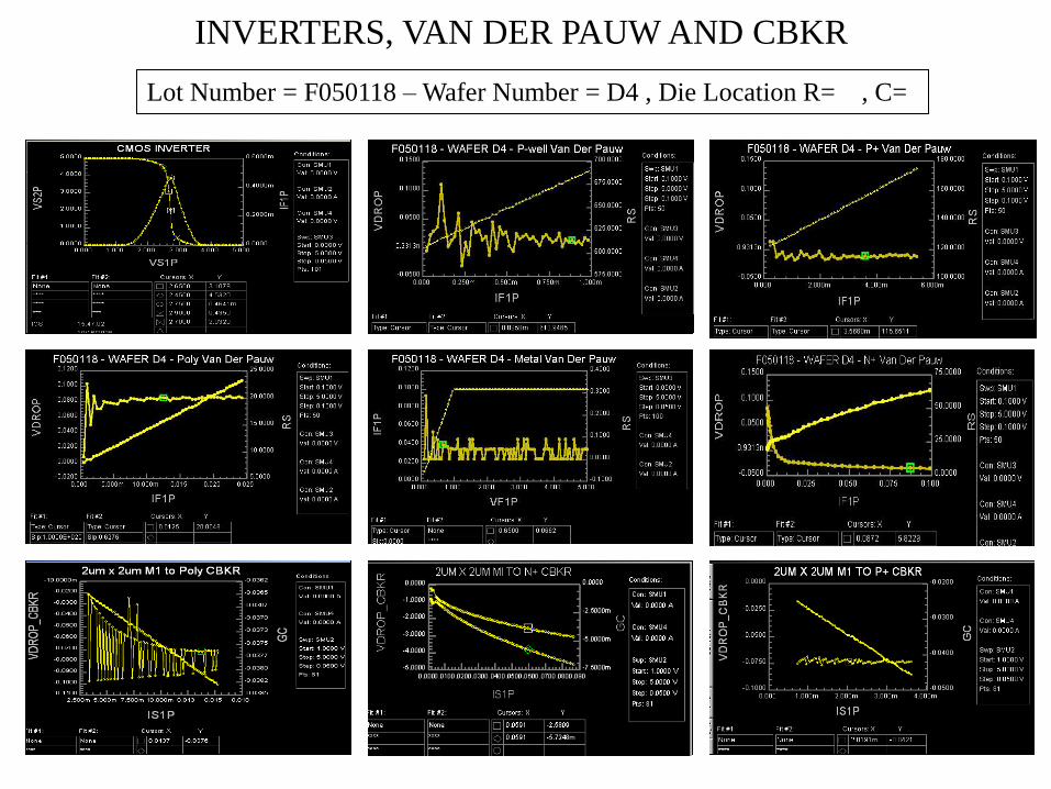
M1 to Poly
CBKR
M1 to N+
CBKR
M1 to P+
CBKR
N+
Van Der Pauw
P+
Van Der Pauw
P-Well
Van Der Pauw
Inverter Poly
Van Der Pauw
M1
Van Der Pauw
INVERTERS, VAN DER PAUW AND CBKR
Lot Number = F050118 – Wafer Number = D4 , Die Location R= , C=
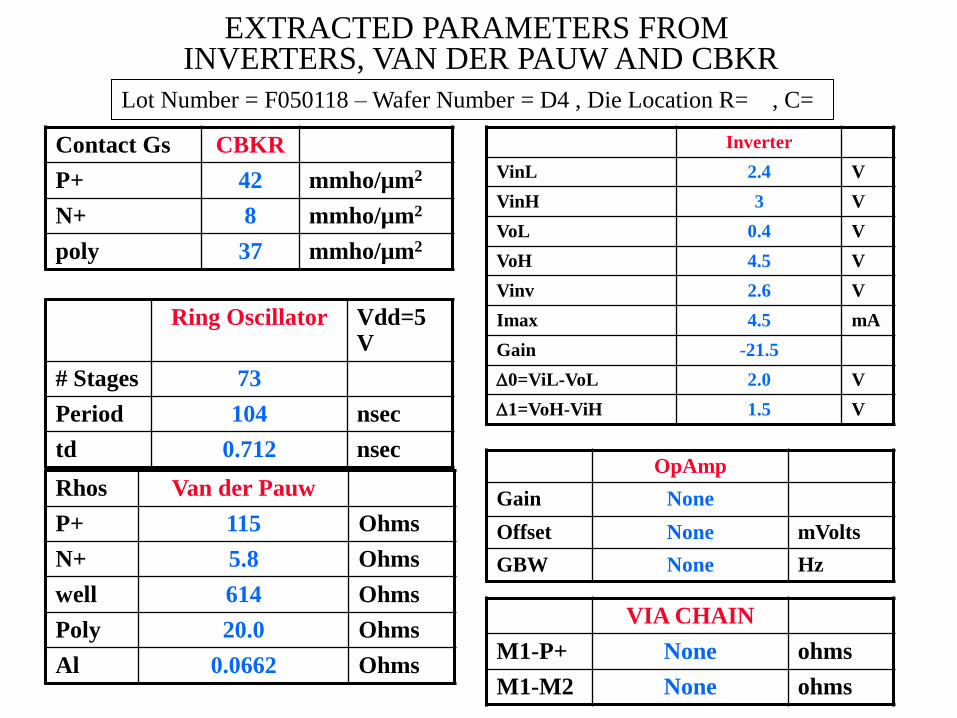
Rhos Van der Pauw
P+ 115 Ohms
N+ 5.8 Ohms
well 614 Ohms
Poly 20.0 Ohms
Al 0.0662 Ohms
Contact Gs CBKR
P+ 42 mmho/µm2
N+ 8 mmho/µm2
poly 37 mmho/µm2
OpAmp
Gain None
Offset None mVolts
GBW None Hz
Ring Oscillator Vdd=5V
# Stages 73
Period 104 nsec
td 0.712 nsec
Inverter
VinL 2.4 V
VinH 3 V
VoL 0.4 V
VoH 4.5 V
Vinv 2.6 V
Imax 4.5 mA
Gain -21.5
0=ViL-VoL 2.0 V
1=VoH-ViH 1.5 V
EXTRACTED PARAMETERS FROM INVERTERS, VAN DER PAUW AND CBKR
Lot Number = F050118 – Wafer Number = D4 , Die Location R= , C=
VIA CHAIN
M1-P+ None ohms
M1-M2 None ohms
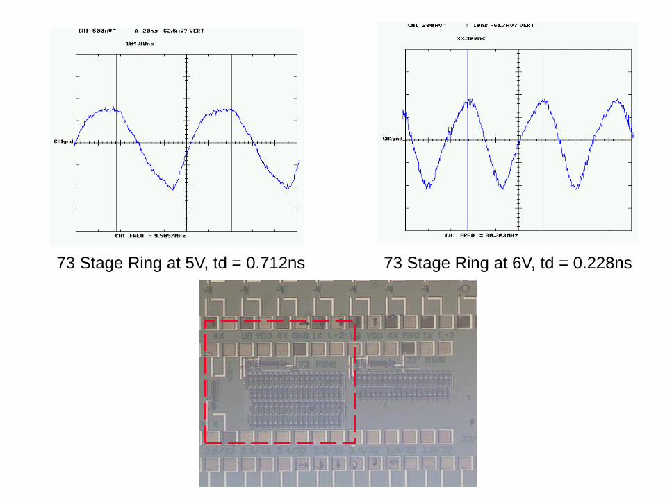
73 Stage Ring at 6V, td = 0.228ns 73 Stage Ring at 5V, td = 0.712ns
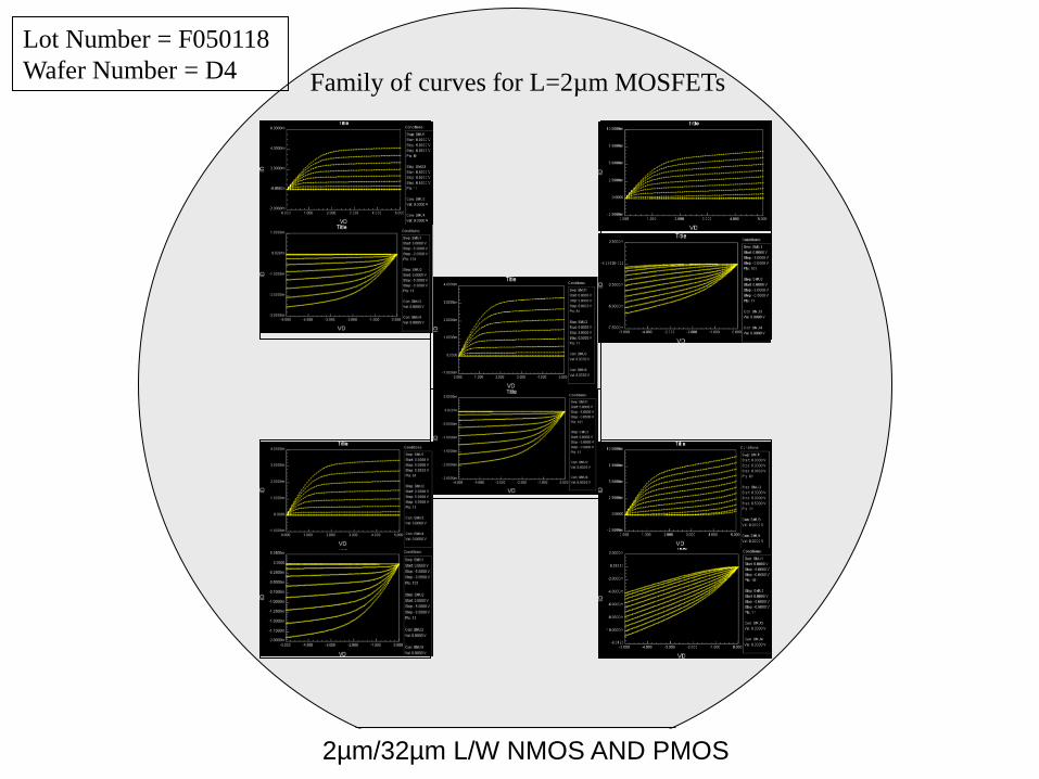
2µm/32µm L/W NMOS AND PMOS
Family of curves for L=2µm MOSFETs
Lot Number = F050118
Wafer Number = D4
© April 30, 2015, Dr. Lynn Fuller, Professor
CMOS Testing
Page 57
Rochester Institute of Technology
Microelectronic Engineering
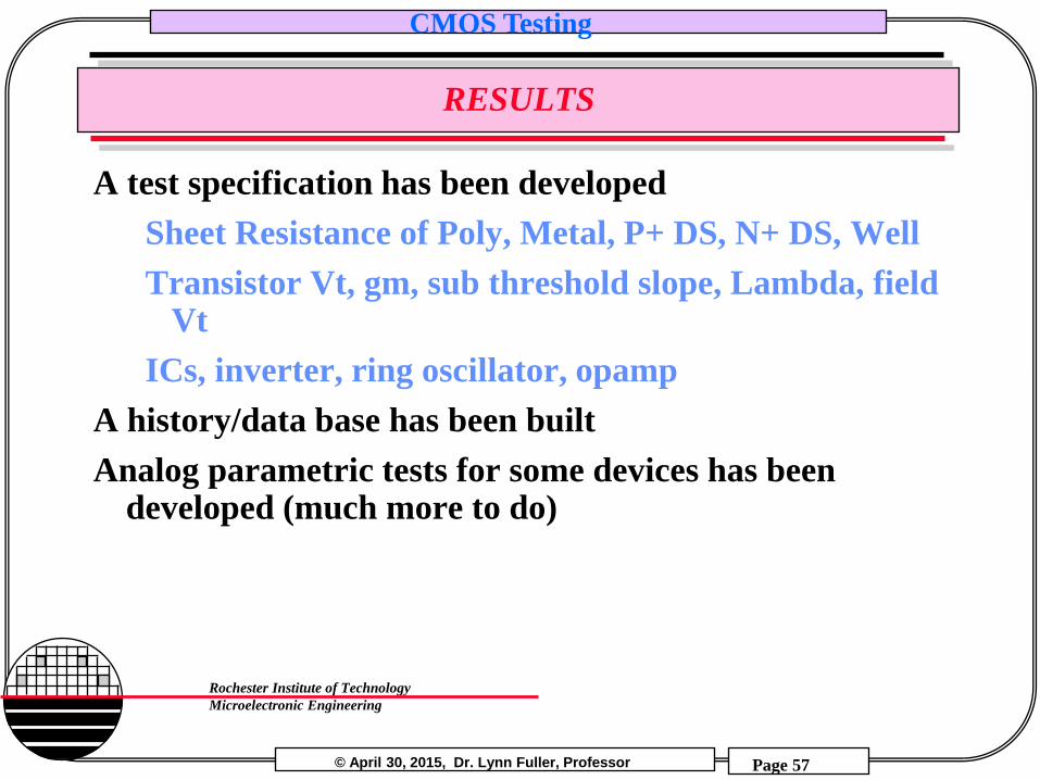
RESULTS
A test specification has been developed
Sheet Resistance of Poly, Metal, P+ DS, N+ DS, Well
Transistor Vt, gm, sub threshold slope, Lambda, field Vt
ICs, inverter, ring oscillator, opamp
A history/data base has been built
Analog parametric tests for some devices has been developed (much more to do)
© April 30, 2015, Dr. Lynn Fuller, Professor
CMOS Testing
Page 58
Rochester Institute of Technology
Microelectronic Engineering
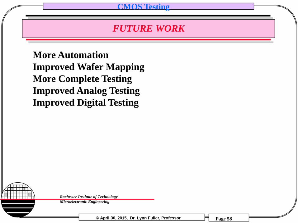
FUTURE WORK
More Automation
Improved Wafer Mapping
More Complete Testing
Improved Analog Testing
Improved Digital Testing
© April 30, 2015, Dr. Lynn Fuller, Professor
CMOS Testing
Page 59
Rochester Institute of Technology
Microelectronic Engineering
CONCLUSION
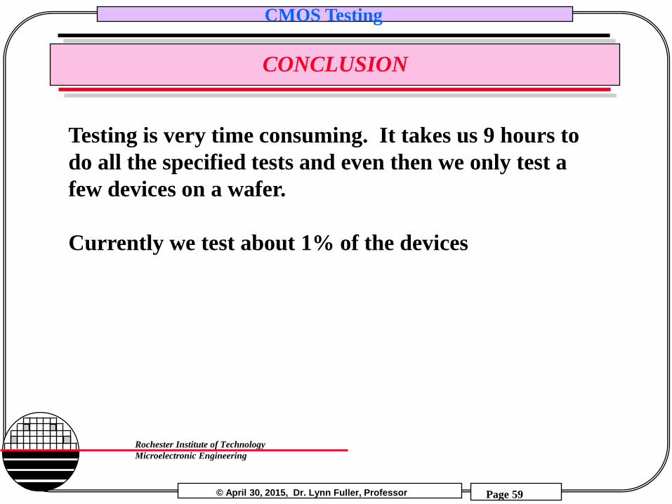
Testing is very time consuming. It takes us 9 hours to
do all the specified tests and even then we only test a
few devices on a wafer.
Currently we test about 1% of the devices
© April 30, 2015, Dr. Lynn Fuller, Professor
CMOS Testing
Page 60
Rochester Institute of Technology
Microelectronic Engineering
HOMEWORK – CMOS TEST
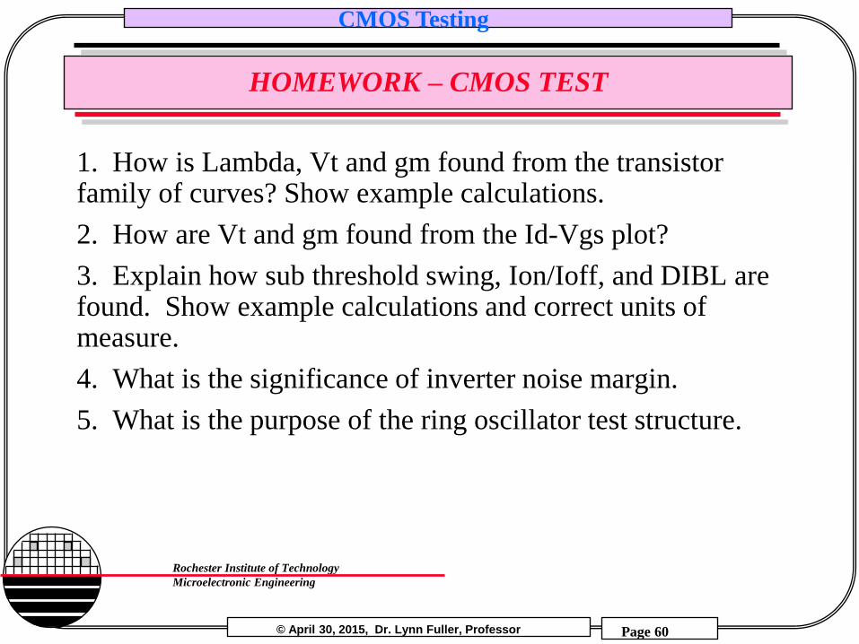
1. How is Lambda, Vt and gm found from the transistor family of curves? Show example calculations.
2. How are Vt and gm found from the Id-Vgs plot?
3. Explain how sub threshold swing, Ion/Ioff, and DIBL are found. Show example calculations and correct units of measure.
4. What is the significance of inverter noise margin.
5. What is the purpose of the ring oscillator test structure.
© April 30, 2015, Dr. Lynn Fuller, Professor
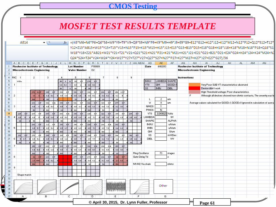
CMOS Testing
Page 61
Rochester Institute of Technology
Microelectronic Engineering
MOSFET TEST RESULTS TEMPLATE