Embed Size (px)
Citation preview
2168-6777 (c) 2020 IEEE. Personal use is permitted, but republication/redistribution requires IEEE permission. See http://www.ieee.org/publications_standards/publications/rights/index.html for more information.
This article has been accepted for publication in a future issue of this journal, but has not been fully edited. Content may change prior to final publication. Citation information: DOI 10.1109/JESTPE.2020.3037886, IEEE Journalof Emerging and Selected Topics in Power Electronics
Special Issue on Electric Machine Drives and Converters for Automotive Applications
Common-mode Voltage Reduction in VSI-fed Motor
Drives with An Integrated Active Zero-state Switch
Zhe Zhang, Student Member, IEEE, Ali M. Bazzi, Senior Member, IEEE
Abstract- Common-mode voltage produced by voltage source
inverters (VSI) is of great concern in motor drive systems.
Significant amount of conducted common-mode/bearing current
will be induced and will interfere with system operation. As an
alternative to inserting bulky passive filters to combat the
adverse effect by common-mode voltage, this paper proposes a
new topology of integrated active zero-state switch (IAZS). Minor
adjustment to the standard space vector pulse-width modulation
(SVPWM) is proposed to facilitate the use of IAZS, which
enables common-mode voltage reduction in VSI-fed motor
drives. Simulation and experimental results on a commercial VSI
are presented as proof of concept to validate the effectiveness of
proposed design in common-mode voltage reduction.
Index Terms- Voltage source inverter (VSI), motor drive, space
vector pulse-width modulation (SVPWM), common-mode voltage
(CMV) reduction.
I. INTRODUCTION
Adjustable speed drives (ASDs), also known as variable
frequency drives (VFDs), have become popular in industrial,
commercial and residential applications. They have been on
the market for decades and have a wide range of applications
ranging from motor-driven pumps, fans and compressors to
highly sophisticated electrified transportation systems. As
shown in Fig. 1, a typical motor drive system consists of
power conversion unit, power cables and a motor [1], in
addition to controllers and all necessary sensors (not shown in
the figure).
Front-end DC-link Inverter
3-ph cables Motor
Ground
Source
Power Conversion Unit
Fig. 1. Schematic of motor drive system.
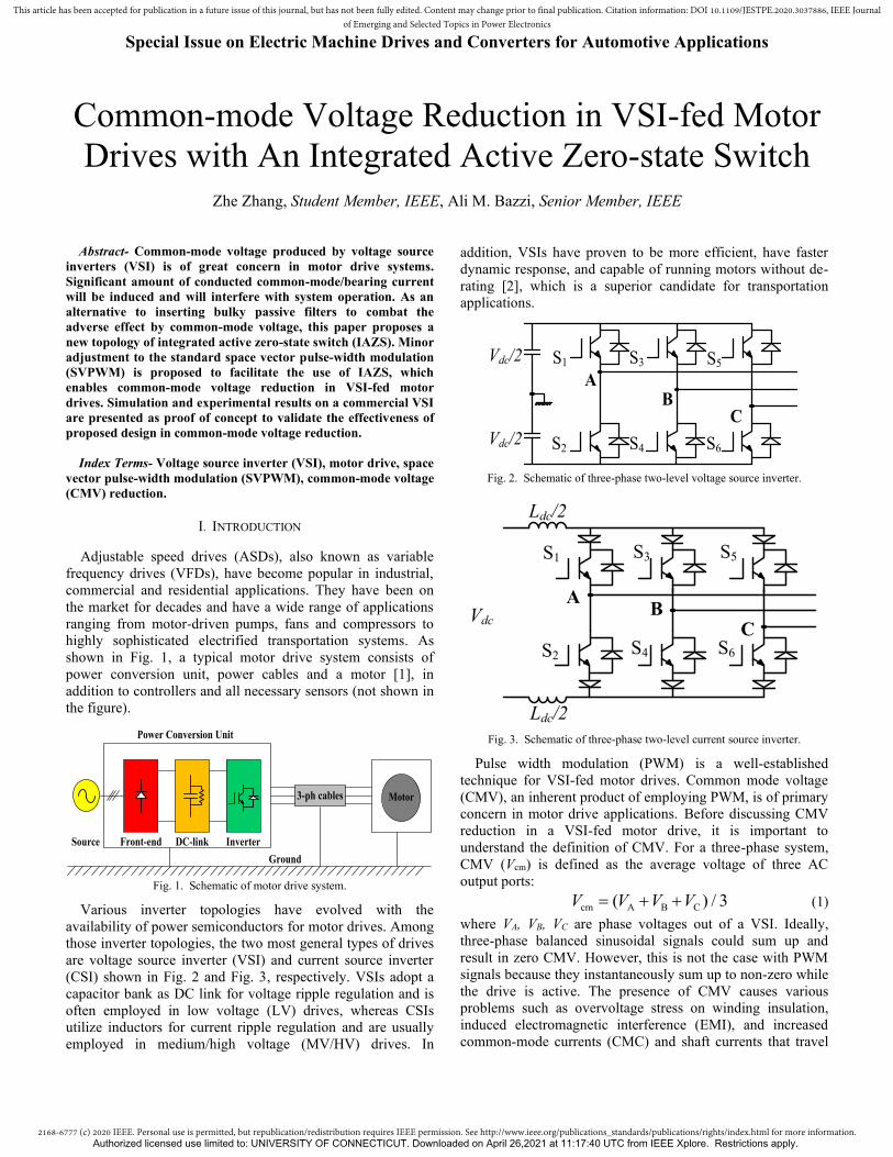
Various inverter topologies have evolved with the
availability of power semiconductors for motor drives. Among
those inverter topologies, the two most general types of drives
are voltage source inverter (VSI) and current source inverter
(CSI) shown in Fig. 2 and Fig. 3, respectively. VSIs adopt a
capacitor bank as DC link for voltage ripple regulation and is
often employed in low voltage (LV) drives, whereas CSIs
utilize inductors for current ripple regulation and are usually
employed in medium/high voltage (MV/HV) drives. In
addition, VSIs have proven to be more efficient, have faster
dynamic response, and capable of running motors without de-
rating [2], which is a superior candidate for transportation
applications.
AB
S1
S2
S3
S4
S5
S6
C
Vdc/2
Vdc/2
Fig. 2. Schematic of three-phase two-level voltage source inverter.
AB
S1
S2
S3
S4
S5
S6
CVdc
Ldc/2
Ldc/2
Fig. 3. Schematic of three-phase two-level current source inverter.
Pulse width modulation (PWM) is a well-established
technique for VSI-fed motor drives. Common mode voltage
(CMV), an inherent product of employing PWM, is of primary
concern in motor drive applications. Before discussing CMV
reduction in a VSI-fed motor drive, it is important to
understand the definition of CMV. For a three-phase system,
CMV (Vcm) is defined as the average voltage of three AC
output ports:
cm A B C( ) / 3V V V V= + + (1)
where VA, VB, VC are phase voltages out of a VSI. Ideally,
three-phase balanced sinusoidal signals could sum up and
result in zero CMV. However, this is not the case with PWM
signals because they instantaneously sum up to non-zero while
the drive is active. The presence of CMV causes various
problems such as overvoltage stress on winding insulation,
induced electromagnetic interference (EMI), and increased
common-mode currents (CMC) and shaft currents that travel
Authorized licensed use limited to: UNIVERSITY OF CONNECTICUT. Downloaded on April 26,2021 at 11:17:40 UTC from IEEE Xplore. Restrictions apply.
2168-6777 (c) 2020 IEEE. Personal use is permitted, but republication/redistribution requires IEEE permission. See http://www.ieee.org/publications_standards/publications/rights/index.html for more information.
This article has been accepted for publication in a future issue of this journal, but has not been fully edited. Content may change prior to final publication. Citation information: DOI 10.1109/JESTPE.2020.3037886, IEEE Journalof Emerging and Selected Topics in Power Electronics
Special Issue on Electric Machine Drives and Converters for Automotive Applications
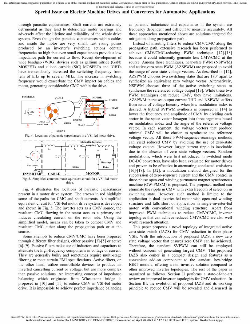
through parasitic capacitances. Shaft currents are extremely
detrimental as they tend to deteriorate motor bearings and
adversely affect the lifetime and reliability of the whole drive
system. Even though the parasitic capacitances within cables
and inside the motor are very small, fast rising pulses
produced by an inverter’s switching actions contain
frequencies so high that even small capacitances provide a low
impedance path for current to flow. Recent development of
wide bandgap (WBG) devices such as gallium nitride (GaN)
MOSFETs and silicon carbide (SiC) MOSFETs and IGBTs
have tremendously increased the switching frequency from
tens of kHz up to several MHz. The increase in switching
frequency would exacerbate the CMV impact on cables and
motor, generating considerable CMC within the drive.
INVERTERCABLE MOTOR
CABLE
CONDUCTORSHIELD
ROTOR
STATOR
FRAME
BEARING
SHAFT
GROUND
Fig. 4. Locations of parasitic capacitances in a VSI-fed motor drive.
Vcm
Cinv
Lc
Cc
Ls
Cs
Lr
Bearings
Mutual inductance
coupling
Stator Rotor
INVERTER CABLE MOTOR
Fig. 5. Simplified common-mode equivalent circuit for a VSI-fed motor
drive.
Fig. 4 illustrates the locations of parasitic capacitances
present in a motor drive system. The arrows in red highlight
some of the paths for CMC and shaft currents. A simplified
equivalent circuit for VSI-fed motor drive system is developed
and shown in Fig. 5. The inverter acts as a CMV source, the
resultant CMC flowing in the stator acts as a primary and
induces circulating current on the rotor side. Using the
simplified model, means can be taken to combat CMV and
resultant CMC either along the propagation path or at the
source.
Some attempts to reduce CMV/CMC have been proposed
through different filter designs, either passive [3]-[5] or active
[6]-[9]. Passive filters make use of inductors and capacitors to
attenuate the high-frequency components in voltage or current.
They are generally bulky and sometimes require multi-stage
filtering to meet certain EMI specifications. Active filters, on
the other hand, utilize controllable devices to produce an
inverted cancelling current or voltage, but are more complex
than passive solutions. An interesting concept of impedance
balancing which originates from Wheatstone bridge is
proposed in [10] and [11] to reduce CMV in VSI-fed motor
drive. It is impossible to achieve perfect impedance balancing
as parasitic inductance and capacitance in the system are
frequency dependent and difficult to measure accurately. All
these approaches mentioned above are solutions targeted for
mitigation along propagation path.
Instead of inserting filters to reduce CMV/CMC along the
propagation path, extensive research has been performed to
achieve CMV/CMC-reducing PWM technique [12]-[18]
because it could inherently generate less CMV/CMC at the
source. Among those techniques, near-state PWM (NSPWM)
and active zero state PWM (AZSPWM) are proposed to avoid
the usage of zero-state voltage vectors. As described in [12],
AZSPWM chooses two switching states that are 180˚ apart to
synthesize an equivalent zero voltage vector. Alternatively,
NSPWM chooses three of the active switching states to
synthesize the referenced voltage output [13]. While these two
PWM techniques can reduce CMV, they have limitations.
AZSPWM increases output current THD and NSPWM suffers
from issue of voltage linearity when low modulation index is
desired. A hybrid SVPWM synthesis is proposed in [14] to
lower the frequency and amplitude of CMV by dividing each
sector in the space vector hexagon into three segments based
on modulation index and the angle of the reference voltage
vector. In each segment, the voltage vectors that produce
minimal CMV will be chosen to synthesize the reference
voltage vector. All these PWM-sequence-rearrange methods
can yield reduced CMV by avoiding the use of zero-state
voltage vectors. However, larger current ripple is inevitable
due to the absence of zero state voltage vectors. Random
modulations, which were first introduced in switched mode
DC-DC converters, have also been evaluated for motor drives
and proven to be effective in attenuating conducted emissions
[16]-[18]. In [32], a modulation method designed for the
suppression of zero-sequence current and the CMV control in
three-phase open-end winding permanent magnet synchronous
machine (OW-PMSM) is proposed. The proposed method can
eliminate the ripple in CMV with extra freedom of selection in
switching state. However, such method is limited to the
application in dual-inverter-fed motor with open-end winding
structure and falls short of application in single-inverter-fed
motor with conventional winding structure. Apart from
improved PWM techniques to reduce CMV/CMC, inverter
topologies that can achieve reduced CMV/CMC are also well
worth research attention.
This paper proposes a novel topology of integrated active
zero-state switch (IAZS) for CMV reduction in three-phase
VSIs. With the introduction of proposed IAZS, a new zero
state voltage vector that ensures zero CMV can be achieved.
Therefore, the standard SVPWM can still be employed
without concern of generating largest CMV. The proposed
IAZS also comes in a compact design and features as a
convenient add-on component to the standard hex-bridge
IGBT module, offering a non-invasive solution compared to
other improved inverter topologies. The rest of the paper is
organized as follows. Section II performs a state-of-the-art
review on improved inverter topologies for CMV reduction. In
Section III, the evolution of proposed IAZS and its working
principle to reduce CMV will be revealed and discussed in
Authorized licensed use limited to: UNIVERSITY OF CONNECTICUT. Downloaded on April 26,2021 at 11:17:40 UTC from IEEE Xplore. Restrictions apply.
2168-6777 (c) 2020 IEEE. Personal use is permitted, but republication/redistribution requires IEEE permission. See http://www.ieee.org/publications_standards/publications/rights/index.html for more information.
This article has been accepted for publication in a future issue of this journal, but has not been fully edited. Content may change prior to final publication. Citation information: DOI 10.1109/JESTPE.2020.3037886, IEEE Journalof Emerging and Selected Topics in Power Electronics
Special Issue on Electric Machine Drives and Converters for Automotive Applications
detail. Simulation and experimental results are presented in
Section IV. Section V concludes the paper.
II. REVIEW OF IMPROVED INVERTER TOPOLOGIES IN
MOTOR DRIVES FOR CMV REDUCTION
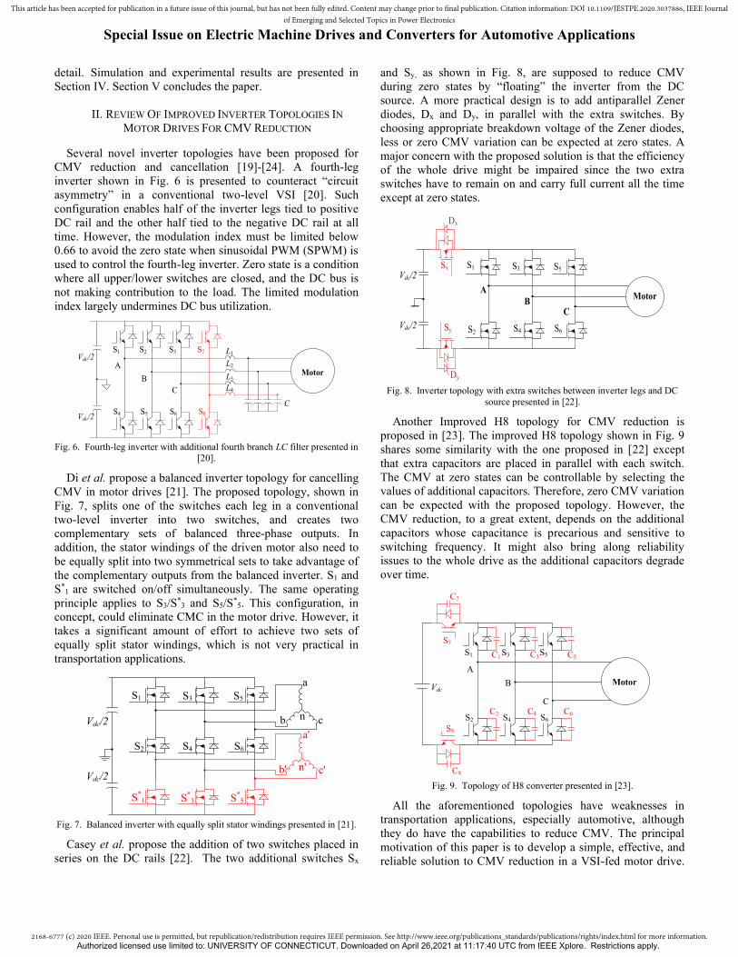
Several novel inverter topologies have been proposed for
CMV reduction and cancellation [19]-[24]. A fourth-leg
inverter shown in Fig. 6 is presented to counteract “circuit
asymmetry” in a conventional two-level VSI [20]. Such
configuration enables half of the inverter legs tied to positive
DC rail and the other half tied to the negative DC rail at all
time. However, the modulation index must be limited below
0.66 to avoid the zero state when sinusoidal PWM (SPWM) is
used to control the fourth-leg inverter. Zero state is a condition
where all upper/lower switches are closed, and the DC bus is
not making contribution to the load. The limited modulation
index largely undermines DC bus utilization.
Vdc/2
Vdc/2
Motor
S1 S2 S3
S4 S5 S6
S7
S8
L1
L2
L3
C
L4
A
B
C
Fig. 6. Fourth-leg inverter with additional fourth branch LC filter presented in
[20].
Di et al. propose a balanced inverter topology for cancelling
CMV in motor drives [21]. The proposed topology, shown in
Fig. 7, splits one of the switches each leg in a conventional
two-level inverter into two switches, and creates two
complementary sets of balanced three-phase outputs. In
addition, the stator windings of the driven motor also need to
be equally split into two symmetrical sets to take advantage of
the complementary outputs from the balanced inverter. S1 and
S*1 are switched on/off simultaneously. The same operating
principle applies to S3/S*3 and S5/S*
5. This configuration, in
concept, could eliminate CMC in the motor drive. However, it
takes a significant amount of effort to achieve two sets of
equally split stator windings, which is not very practical in
transportation applications.
Vdc/2
Vdc/2
S1
S2
S*
1
S3 S5
S4 S6
S*
3 S*
5
n
n'
a
b c
a'
b' c'
Fig. 7. Balanced inverter with equally split stator windings presented in [21].
Casey et al. propose the addition of two switches placed in
series on the DC rails [22]. The two additional switches Sx
and Sy, as shown in Fig. 8, are supposed to reduce CMV
during zero states by “floating” the inverter from the DC
source. A more practical design is to add antiparallel Zener
diodes, Dx and Dy, in parallel with the extra switches. By
choosing appropriate breakdown voltage of the Zener diodes,
less or zero CMV variation can be expected at zero states. A
major concern with the proposed solution is that the efficiency
of the whole drive might be impaired since the two extra
switches have to remain on and carry full current all the time
except at zero states.
A
B
S1
S2
S3
S4
S5
S6
C
Vdc/2
Vdc/2
Dx
Sx
Sy
Dy
Motor
Fig. 8. Inverter topology with extra switches between inverter legs and DC
source presented in [22].
Another Improved H8 topology for CMV reduction is
proposed in [23]. The improved H8 topology shown in Fig. 9
shares some similarity with the one proposed in [22] except
that extra capacitors are placed in parallel with each switch.
The CMV at zero states can be controllable by selecting the
values of additional capacitors. Therefore, zero CMV variation
can be expected with the proposed topology. However, the
CMV reduction, to a great extent, depends on the additional
capacitors whose capacitance is precarious and sensitive to
switching frequency. It might also bring along reliability
issues to the whole drive as the additional capacitors degrade
over time.
Motor
A
B
C
S3
S4
S5
S6
S1
S2
Vdc
S7
S8
C8
C7
C1 C3 C5
C2 C4 C6
Fig. 9. Topology of H8 converter presented in [23].
All the aforementioned topologies have weaknesses in
transportation applications, especially automotive, although
they do have the capabilities to reduce CMV. The principal
motivation of this paper is to develop a simple, effective, and
reliable solution to CMV reduction in a VSI-fed motor drive.
Authorized licensed use limited to: UNIVERSITY OF CONNECTICUT. Downloaded on April 26,2021 at 11:17:40 UTC from IEEE Xplore. Restrictions apply.
2168-6777 (c) 2020 IEEE. Personal use is permitted, but republication/redistribution requires IEEE permission. See http://www.ieee.org/publications_standards/publications/rights/index.html for more information.
This article has been accepted for publication in a future issue of this journal, but has not been fully edited. Content may change prior to final publication. Citation information: DOI 10.1109/JESTPE.2020.3037886, IEEE Journalof Emerging and Selected Topics in Power Electronics
Special Issue on Electric Machine Drives and Converters for Automotive Applications
The development of proposed topology is explained in the
following section.
III. DESIGN OF PROPOSED TOPOLOGY FOR CMV
REDUCTION IN A VSI-FED MOTOR DRIVE
As stated in the previous section, the DC bus does not
contribute to the load at zero state where all upper/lower
switches are closed in a conventional two-level VSI. Zero
states are desirable and necessary for synthesis of referenced
voltage. The avoidance of synthesizing referenced voltage
with zero states would result in distorted current output [25].
For ease of analysis, the mid-point of the DC bus is referenced
as ground. The main scope of this paper is to develop a new
topology that preserves the use of zero states in referenced
voltage synthesis without generating considerable CMV [26].
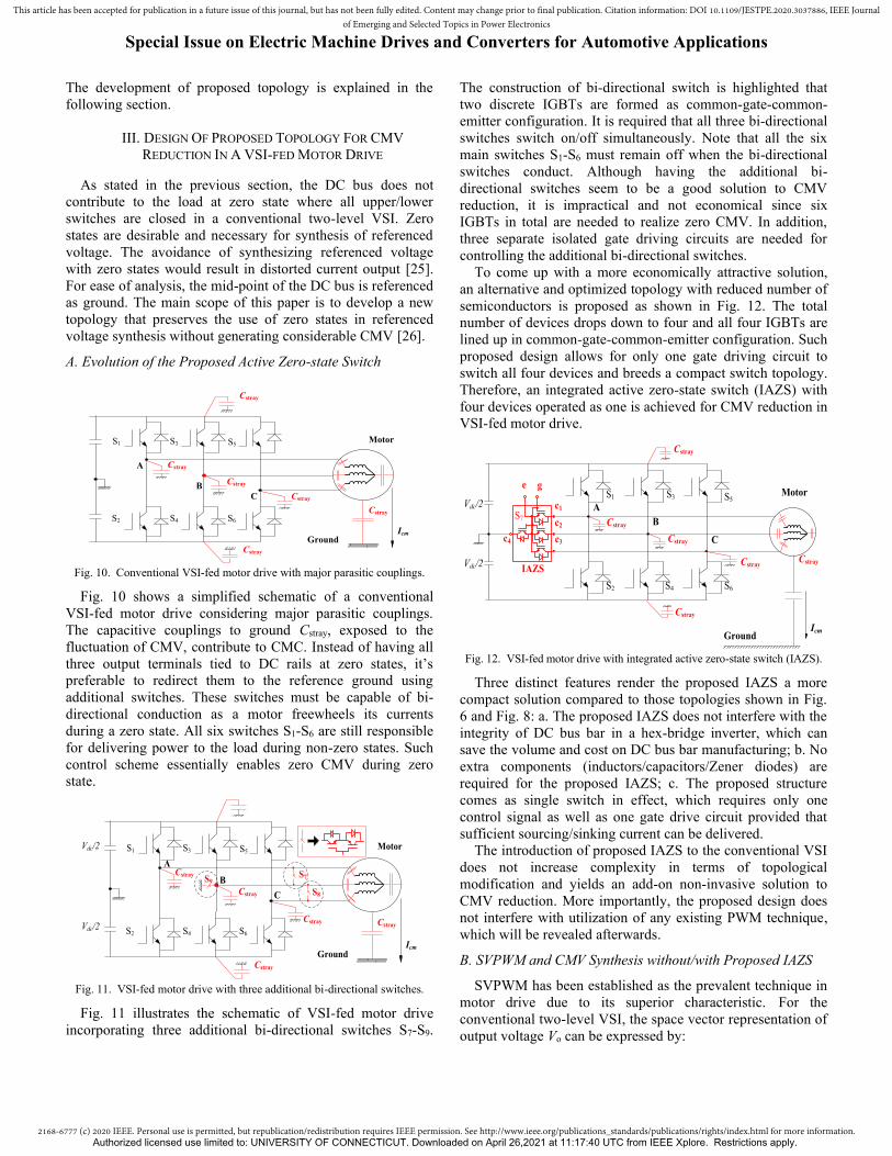
A. Evolution of the Proposed Active Zero-state Switch
Cstray
A
B
Ground
S1
S2
S3
S4
S5
S6
C
Icm
Cstray
Cstray
Cstray
Cstray
Cstray
Motor
Fig. 10. Conventional VSI-fed motor drive with major parasitic couplings.
Fig. 10 shows a simplified schematic of a conventional
VSI-fed motor drive considering major parasitic couplings.
The capacitive couplings to ground Cstray, exposed to the
fluctuation of CMV, contribute to CMC. Instead of having all
three output terminals tied to DC rails at zero states, it’s
preferable to redirect them to the reference ground using
additional switches. These switches must be capable of bi-
directional conduction as a motor freewheels its currents
during a zero state. All six switches S1-S6 are still responsible
for delivering power to the load during non-zero states. Such
control scheme essentially enables zero CMV during zero
state.
A
B
Ground
S1
S2
S3
S4
S5
S6
C
Icm
Cstray
Vdc/2
Vdc/2
Cstray
Cstray
Cstray
Cstray
S7
S8
S9
Motor
Fig. 11. VSI-fed motor drive with three additional bi-directional switches.
Fig. 11 illustrates the schematic of VSI-fed motor drive
incorporating three additional bi-directional switches S7-S9.
The construction of bi-directional switch is highlighted that
two discrete IGBTs are formed as common-gate-common-
emitter configuration. It is required that all three bi-directional
switches switch on/off simultaneously. Note that all the six
main switches S1-S6 must remain off when the bi-directional
switches conduct. Although having the additional bi-
directional switches seem to be a good solution to CMV
reduction, it is impractical and not economical since six
IGBTs in total are needed to realize zero CMV. In addition,
three separate isolated gate driving circuits are needed for
controlling the additional bi-directional switches.
To come up with a more economically attractive solution,
an alternative and optimized topology with reduced number of
semiconductors is proposed as shown in Fig. 12. The total
number of devices drops down to four and all four IGBTs are
lined up in common-gate-common-emitter configuration. Such
proposed design allows for only one gate driving circuit to
switch all four devices and breeds a compact switch topology.
Therefore, an integrated active zero-state switch (IAZS) with
four devices operated as one is achieved for CMV reduction in
VSI-fed motor drive.
A
B
Ground
S1
S2
S3
S4
S5
S6
C
Icm
Cstray
Cstray
Cstray
Cstray
Cstray
Cstray
Motorge
c1
c2
c3c4
S7
Vdc/2
Vdc/2 IAZS
Fig. 12. VSI-fed motor drive with integrated active zero-state switch (IAZS).
Three distinct features render the proposed IAZS a more
compact solution compared to those topologies shown in Fig.
6 and Fig. 8: a. The proposed IAZS does not interfere with the
integrity of DC bus bar in a hex-bridge inverter, which can
save the volume and cost on DC bus bar manufacturing; b. No
extra components (inductors/capacitors/Zener diodes) are
required for the proposed IAZS; c. The proposed structure
comes as single switch in effect, which requires only one
control signal as well as one gate drive circuit provided that
sufficient sourcing/sinking current can be delivered.
The introduction of proposed IAZS to the conventional VSI
does not increase complexity in terms of topological
modification and yields an add-on non-invasive solution to
CMV reduction. More importantly, the proposed design does
not interfere with utilization of any existing PWM technique,
which will be revealed afterwards.
B. SVPWM and CMV Synthesis without/with Proposed IAZS
SVPWM has been established as the prevalent technique in
motor drive due to its superior characteristic. For the
conventional two-level VSI, the space vector representation of
output voltage Vo can be expressed by:
Authorized licensed use limited to: UNIVERSITY OF CONNECTICUT. Downloaded on April 26,2021 at 11:17:40 UTC from IEEE Xplore. Restrictions apply.
2168-6777 (c) 2020 IEEE. Personal use is permitted, but republication/redistribution requires IEEE permission. See http://www.ieee.org/publications_standards/publications/rights/index.html for more information.
This article has been accepted for publication in a future issue of this journal, but has not been fully edited. Content may change prior to final publication. Citation information: DOI 10.1109/JESTPE.2020.3037886, IEEE Journalof Emerging and Selected Topics in Power Electronics
Special Issue on Electric Machine Drives and Converters for Automotive Applications
2 2
3 3o A B C
2( )
3
j j
V V V e V e −
= + + (2)
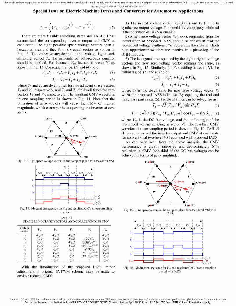
There are eight feasible switching states and TABLE I has
summarized the corresponding inverter output and CMV at
each state. The eight possible space voltage vectors span a
hexagonal area and they form six equal sectors as shown in
Fig. 13. To synthesize any desired output voltage Vref at each
sampling period Ts, the principle of volt-seconds equality
should be applied. For instance, Vref locates in sector VI as
shown in Fig. 13. Consequently, eq. (3) and (4) hold:
ref 5 5 4 4 0 0 7 7+sV T V T V T V T V T= + + (3)
5 4 0 7+sT T T T T= + + (4)
where T5 and T4 are dwell times for two adjacent space vectors
V5 and V4, respectively, and T0 and T7 are dwell times for zero
vectors V0 and V7, respectively. The resultant CMV waveform
in one sampling period is shown in Fig. 14. Note that the
utilization of zero vectors will cause the CMV of highest
magnitude, which corresponds to operating the inverter at zero
states.
V0 (000)V7 (111) V4(100)
V6 (110)V2 (010)
V3 (011)
V1 (001) V5 (101)
I
II
III
IV
V
VI
VrefθVI
Fig. 13. Eight space voltage vectors in the complex plane for a two-level VSI.
S1
S3
S5
Vcm
-Vdc / 2-Vdc / 6
Vdc / 6Vdc / 2
Ts
T0/2 T7 T0/2T5/2T4/2 T5/2 T4/2
Fig. 14. Modulation sequence for Vref and resultant CMV in one sampling
period.
TABLE I
FEASIBLE VOLTAGE VECTORS AND CORRESPONDING CMV
Voltage
vector VA VB VC Vo Vcm
V0 -Vdc/2 -Vdc/2 -Vdc/2 0 -Vdc/2
V4 Vdc/2 -Vdc/2 -Vdc/2 (2/3)Vdc -Vdc/6
V6 Vdc/2 Vdc/2 -Vdc/2 (2/3)Vdcej(π/3) Vdc/6
V2 -Vdc/2 Vdc/2 -Vdc/2 (2/3)Vdcej(2π/3) -Vdc/6
V3 -Vdc/2 Vdc/2 Vdc/2 -(2/3)Vdc Vdc/6
V1 -Vdc/2 -Vdc/2 Vdc/2 (2/3)Vdcej(4π/3) -Vdc/6
V5 Vdc/2 -Vdc/2 Vdc/2 (2/3)Vdcej(5π/3) Vdc/6
V7 Vdc/2 Vdc/2 Vdc/2 0 Vdc/2
With the introduction of the proposed IAZS, minor
adjustment to original SVPWM scheme must be made to
achieve reduced CMV:
1) The use of voltage vector V0 (0000) and V7 (0111) to
synthesize output voltage Vref should be completely inhibited
if the operation of IAZS is enabled.
2) A new zero voltage vector V8 (1xxx), originated from the
introduction of proposed IAZS, should be chosen instead for
referenced voltage synthesis. “x” represents the state in which
both upper/lower switches are inactive in a phase-leg of the
IGBT module.
3) The hexagonal area spanned by the eight original voltage
vectors and new zero voltage vector remains the same, as
shown in Fig. 15. Similarly, for Vref residing in sector VI, the
following eq. (5) and (6) hold:
ref 5 5 4 4 8 8sV T V T V T V T= + + (5)
5 4 8sT T T T= + + (6)
where T8 is the dwell time for new zero voltage vector V8
when the proposed IAZS is in use. By equating the real and
imaginary part in eq. (5), the dwell times can be solved for as:
4 3( / )sinref dc VI sT V V T= (7)
5 ( 3 / 2)( / ) ( 3 cos sin )ref dc s VI VIT V V T = − (8)
where Vdc is the DC bus voltage, and θVI is the angle of the
referenced voltage residing in sector VI. The resultant CMV
waveform in one sampling period is shown in Fig. 16. TABLE
II has summarized the inverter output and CMV at each state
for conventional two-level VSI equipped with proposed IAZS.
As can been seen from the above analysis, the CMV
performance is greatly improved and approximately 67%
reduction in CMV (one third of the DC bus voltage) can be
achieved in terms of peak amplitude.
V0 (0000)
V7 (0111) V4(0100)
V6 (0110)V2 (0010)
V3 (0011)
V1 (0001) V5 (0101)
I
II
III
IV
V
VI
Vref
V8 (1xxx)
θVI
Fig. 15. Nine space vectors in the complex plane for a two-level VSI with
IAZS.
Ts
T5/2T4/2 T5/2 T4/2T8/2T8/4 T8/4
Vcm
-Vdc / 60
Vdc / 6
S1
S3
S5
S7
Fig. 16. Modulation sequence for Vref and resultant CMV in one sampling
period with IAZS.
Authorized licensed use limited to: UNIVERSITY OF CONNECTICUT. Downloaded on April 26,2021 at 11:17:40 UTC from IEEE Xplore. Restrictions apply.
2168-6777 (c) 2020 IEEE. Personal use is permitted, but republication/redistribution requires IEEE permission. See http://www.ieee.org/publications_standards/publications/rights/index.html for more information.
This article has been accepted for publication in a future issue of this journal, but has not been fully edited. Content may change prior to final publication. Citation information: DOI 10.1109/JESTPE.2020.3037886, IEEE Journalof Emerging and Selected Topics in Power Electronics
Special Issue on Electric Machine Drives and Converters for Automotive Applications
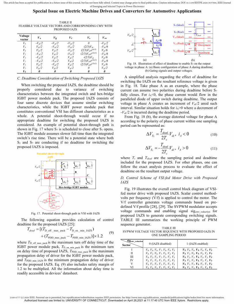
TABLE II FEASIBLE VOLTAGE VECTORS AND CORRESPONDING CMV WITH
PROPOSED IAZS
Voltage
vector VA VB VC Vo Vcm
V0 -Vdc/2 -Vdc/2 -Vdc/2 0 -Vdc/2 V4 Vdc/2 -Vdc/2 -Vdc/2 (2/3)Vdc -Vdc/6
V6 Vdc/2 Vdc/2 -Vdc/2 (2/3)Vdcej(π/3) Vdc/6
V2 -Vdc/2 Vdc/2 -Vdc/2 (2/3)Vdcej(2π/3) -Vdc/6
V3 -Vdc/2 Vdc/2 Vdc/2 -(2/3)Vdc Vdc/6
V1 -Vdc/2 -Vdc/2 Vdc/2 (2/3)Vdcej(4π/3) -Vdc/6
V5 Vdc/2 -Vdc/2 Vdc/2 (2/3)Vdcej(5π/3) Vdc/6
V7 Vdc/2 Vdc/2 Vdc/2 0 Vdc/2
V8 0 0 0 0 0
C. Deadtime Consideration of Switching Proposed IAZS
When switching the proposed IAZS, the deadtime should be
properly considered due to variance of switching
characteristics between the integrated switch and hex-bridge
IGBT power module pack. The proposed IAZS consists of
four same discrete devices that assume similar switching
characteristics, while the IGBT power module pack that
constitutes conventional VSI has different characteristics as a
whole. A potential shoot-through would occur if no
appropriate deadtime for switching the proposed IAZS is
considered. An example of potential shoot-through path is
shown in Fig. 17 where S7 is scheduled to close after S1 opens.
The IGBT module assumes slower fall time than the integrated
switch’s rise time. There will be a potential state where both
S1 and S7 are conducting if no deadtime for switching the
proposed IAZS is imposed.
Potential shoot-through
path
AB
S1
S2
S3
S4
S5
S6
C
Vdc/2
Vdc/2IAZS
Hex-bridge IGBT module
S7
Fig. 17. Potential shoot-through path in VSI with IAZS
The following equation provides calculation of control
deadtime for the proposed IAZS [25]:
D_off _ max_ pack D_on _ min_ IAZS
PDD_max_pack PDD_min_IAZS
[( )
( )] 1.2
deadT T T
T T
= −
+ − (9)
where TD_off_max_pack is the maximum turn off delay time of the
IGBT power module pack, TD_on_min_pack is the minimum turn
on delay time of proposed IAZS, TPDD_max_pack is the maximum
propagation delay of driver for the IGBT power module pack,
and TPDD_min_IAZS is the minimum propagation delay of driver
for the proposed IAZS. Eq. (9) also includes safety margin of
1.2 to be multiplied. All the information about delay time is
readily accessible in devices’ datasheet.
S1
S2
Vdc/2
Vdc/2
S7 iA<0
iA>0
A
(a)
iA>0
iA<0
Ts
Tdead
S7 (Ideal)
S7 (Real)
VA (Ideal)
VA (Real)
VA (Real)Increment
Decrement
(b)
Fig. 18. Illustration of effect of deadtime to enable S7 on the output
voltage in phase A: (a) Basic configuration of phase A during deadtime;
(b) Gating signals and output voltages.
A simplified analysis regarding the effect of deadtime for
switching the IAZS on the resultant reference voltage is given
in Fig. 18. Take phase A as an example, where the phase
current can assume two polarities during deadtime before S7
fully closes. For iA<0, the phase current would flow in the
paralleled diode of upper switch during deadtime. The output
voltage in phase A creates an increment of Vdc/2 amid such
interval. Similar situation holds for iA>0 where a decrement of
-Vdc/2 is incurred during the deadtime period.
From Fig. 18 (b), the average distorted voltage for phase A
according to the polarity of phase current within one sampling
period can be represented as:
7, 0
2
deadS dc A
s
TV V i
T = (10)
7- , 0
2
deadS dc A
s
TV V i
T = (11)
where Ts and Tdead are the sampling period and deadtime
included for the proposed IAZS. For other phases, one can
follow the exact analysis process to evaluate the effect of
deadtime on the resultant output voltage.
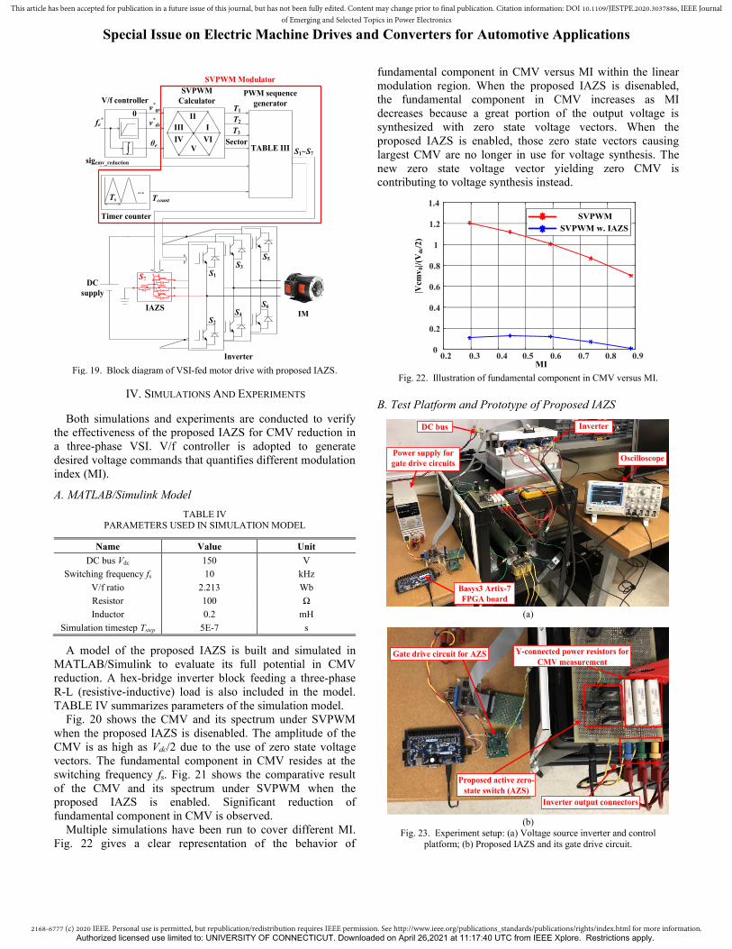
D. Control Scheme of VSI-fed Motor Drive with Proposed
IAZS
Fig. 19 illustrates the overall control block diagram of VSI-
fed motor drive with proposed IAZS. Scalar control method-
volts per frequency (V/f) is applied to control the motor. The
V/f controller generates voltage commands based on pre-
defined V/f profile [28], [29]. The SVPWM modulator accepts
voltage commands and enabling signal sigcmv_reduction for
proposed IAZS to generate corresponding switching signals.
TABLE III summarizes the working principle of PWM
sequence generator. TABLE III
SVPWM VOLTAGE VECTOR SEQUENCE WITH PROPOSED IAZS IN
ONE SAMPLING PERIOD
0 (IAZS disabled) 1 (IAZS enabled)
I V0, V4, V6, V7, V6, V4, V0 V8, V4, V6, V8, V6, V4, V8 II V0, V2, V6, V7, V6, V2, V0 V8, V2, V6, V8, V6, V2, V8
III V0, V2, V3, V7, V3, V2, V0 V8, V2, V3, V8, V3, V2, V8 IV V0, V1, V3, V7, V3, V1, V0 V8, V1, V3, V8, V3, V1, V8
V V0, V1, V5, V7, V5, V1, V0 V8, V1, V5, V8, V5, V1, V8
VI V0, V4, V5, V7, V5, V4, V0 V8, V4, V5, V8, V5, V4, V8
Sector
sigcmv_reduction
Authorized licensed use limited to: UNIVERSITY OF CONNECTICUT. Downloaded on April 26,2021 at 11:17:40 UTC from IEEE Xplore. Restrictions apply.
2168-6777 (c) 2020 IEEE. Personal use is permitted, but republication/redistribution requires IEEE permission. See http://www.ieee.org/publications_standards/publications/rights/index.html for more information.
This article has been accepted for publication in a future issue of this journal, but has not been fully edited. Content may change prior to final publication. Citation information: DOI 10.1109/JESTPE.2020.3037886, IEEE Journalof Emerging and Selected Topics in Power Electronics
Special Issue on Electric Machine Drives and Converters for Automotive Applications
V/f controller
SVPWM
Calculator
Timer counter
PWM sequence
generator
Ts Tcount
Sector
T1
T2
θe
v*
ds
v*
qs 0
fe*
S1~S7
DC
supply
IAZS
Inverter
IM
S7S1
S2
S3
S4
S5
S6
sigcmv_reduction
TABLE III
I
II
III
IVV
VI
SVPWM Modulator
T3
Fig. 19. Block diagram of VSI-fed motor drive with proposed IAZS.
IV. SIMULATIONS AND EXPERIMENTS
Both simulations and experiments are conducted to verify
the effectiveness of the proposed IAZS for CMV reduction in
a three-phase VSI. V/f controller is adopted to generate
desired voltage commands that quantifies different modulation
index (MI).
A. MATLAB/Simulink Model
TABLE IV
PARAMETERS USED IN SIMULATION MODEL
Name Value Unit
DC bus Vdc 150 V
Switching frequency fs 10 kHz
V/f ratio 2.213 Wb
Resistor 100 Ω
Inductor 0.2 mH
Simulation timestep Tstep 5E-7 s
A model of the proposed IAZS is built and simulated in
MATLAB/Simulink to evaluate its full potential in CMV
reduction. A hex-bridge inverter block feeding a three-phase
R-L (resistive-inductive) load is also included in the model.
TABLE IV summarizes parameters of the simulation model.
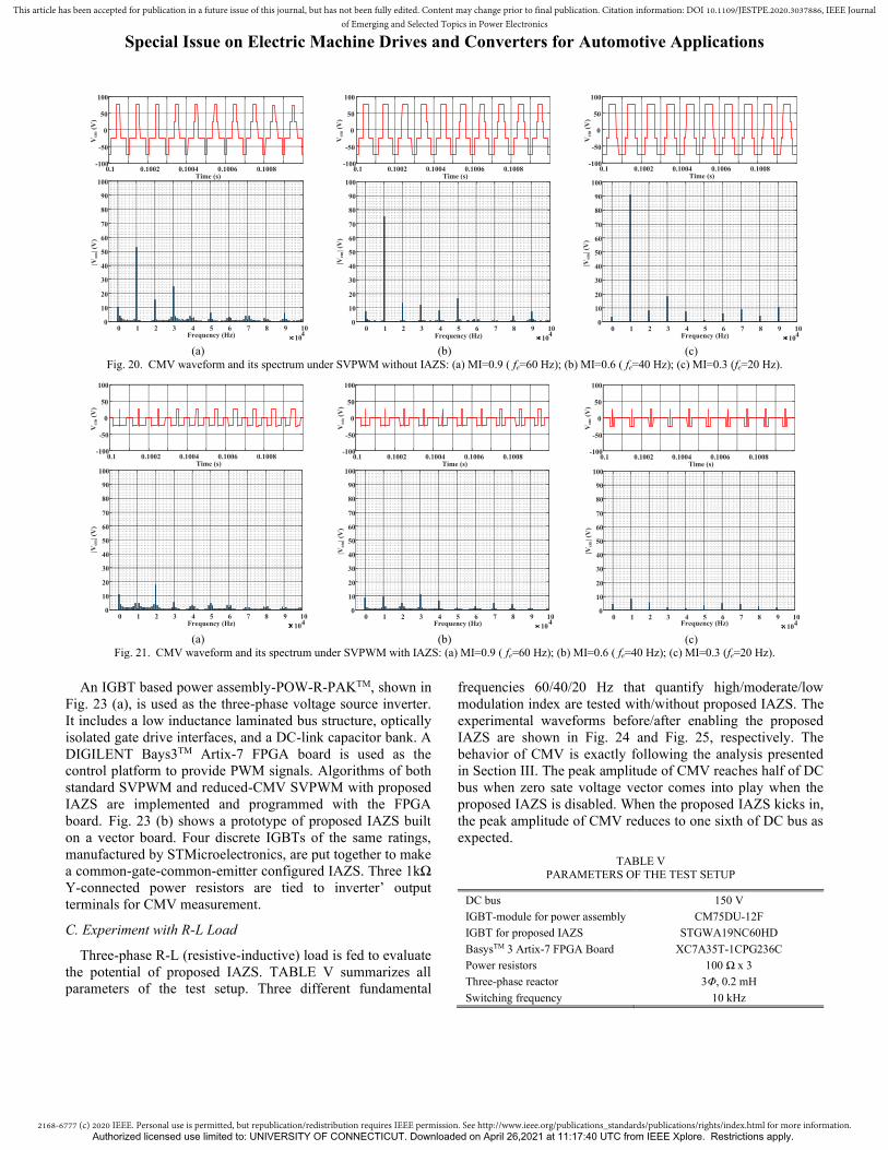
Fig. 20 shows the CMV and its spectrum under SVPWM
when the proposed IAZS is disenabled. The amplitude of the
CMV is as high as Vdc/2 due to the use of zero state voltage
vectors. The fundamental component in CMV resides at the
switching frequency fs. Fig. 21 shows the comparative result
of the CMV and its spectrum under SVPWM when the
proposed IAZS is enabled. Significant reduction of
fundamental component in CMV is observed.
Multiple simulations have been run to cover different MI.
Fig. 22 gives a clear representation of the behavior of
fundamental component in CMV versus MI within the linear
modulation region. When the proposed IAZS is disenabled,
the fundamental component in CMV increases as MI
decreases because a great portion of the output voltage is
synthesized with zero state voltage vectors. When the
proposed IAZS is enabled, those zero state vectors causing
largest CMV are no longer in use for voltage synthesis. The
new zero state voltage vector yielding zero CMV is
contributing to voltage synthesis instead.
0.2 0.3 0.4 0.5 0.6 0.7 0.8 0.90
0.2
0.4
0.6
0.8
1
1.2
1.4
SVPWM
SVPWM w. IAZS
MI
|Vcm
v0|/(V
dc/
2)
Fig. 22. Illustration of fundamental component in CMV versus MI.
B. Test Platform and Prototype of Proposed IAZS
Oscilloscope
Inverter
Basys3 Artix-7
FPGA board
Power supply for
gate drive circuits
DC bus
(a)
Proposed active zero-
state switch (AZS)
Gate drive circuit for AZS
Inverter output connectors
Y-connected power resistors for
CMV measurement
(b)
Fig. 23. Experiment setup: (a) Voltage source inverter and control
platform; (b) Proposed IAZS and its gate drive circuit.
Authorized licensed use limited to: UNIVERSITY OF CONNECTICUT. Downloaded on April 26,2021 at 11:17:40 UTC from IEEE Xplore. Restrictions apply.
2168-6777 (c) 2020 IEEE. Personal use is permitted, but republication/redistribution requires IEEE permission. See http://www.ieee.org/publications_standards/publications/rights/index.html for more information.
This article has been accepted for publication in a future issue of this journal, but has not been fully edited. Content may change prior to final publication. Citation information: DOI 10.1109/JESTPE.2020.3037886, IEEE Journalof Emerging and Selected Topics in Power Electronics
Special Issue on Electric Machine Drives and Converters for Automotive Applications
An IGBT based power assembly-POW-R-PAKTM, shown in
Fig. 23 (a), is used as the three-phase voltage source inverter.
It includes a low inductance laminated bus structure, optically
isolated gate drive interfaces, and a DC-link capacitor bank. A
DIGILENT Bays3TM Artix-7 FPGA board is used as the
control platform to provide PWM signals. Algorithms of both
standard SVPWM and reduced-CMV SVPWM with proposed
IAZS are implemented and programmed with the FPGA
board. Fig. 23 (b) shows a prototype of proposed IAZS built
on a vector board. Four discrete IGBTs of the same ratings,
manufactured by STMicroelectronics, are put together to make
a common-gate-common-emitter configured IAZS. Three 1kΩ
Y-connected power resistors are tied to inverter’ output
terminals for CMV measurement.
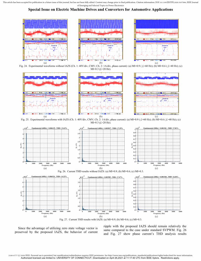
C. Experiment with R-L Load
Three-phase R-L (resistive-inductive) load is fed to evaluate
the potential of proposed IAZS. TABLE V summarizes all
parameters of the test setup. Three different fundamental
frequencies 60/40/20 Hz that quantify high/moderate/low
modulation index are tested with/without proposed IAZS. The
experimental waveforms before/after enabling the proposed
IAZS are shown in Fig. 24 and Fig. 25, respectively. The
behavior of CMV is exactly following the analysis presented
in Section III. The peak amplitude of CMV reaches half of DC
bus when zero sate voltage vector comes into play when the
proposed IAZS is disabled. When the proposed IAZS kicks in,
the peak amplitude of CMV reduces to one sixth of DC bus as
expected.
TABLE V
PARAMETERS OF THE TEST SETUP
DC bus 150 V
IGBT-module for power assembly CM75DU-12F
IGBT for proposed IAZS STGWA19NC60HD
BasysTM 3 Artix-7 FPGA Board XC7A35T-1CPG236C
Power resistors 100 Ω x 3
Three-phase reactor 3Φ, 0.2 mH
Switching frequency 10 kHz
0.1 0.1002 0.1004 0.1006 0.1008Time (s)
-100
-50
0
50
100V
cm (
V)
0 1 2 3 4 5 6 7 8 9 10Frequency (Hz)
0
10
20
30
40
50
60
70
80
90
100
104
|Vcm
| (V
)
(a)
Vcm
(V
)
-1000.1 0.1002 0.1004 0.1006 0.1008
Time (s)
-50
0
50
100
|Vcm
| (V
)
0 1 2 3 4 5 6 7 8 9 10Frequency (Hz) 10
4
0
10
20
30
40
50
60
70
80
90
100
(b)
0.1 0.1002 0.1004 0.1006 0.1008Time (s)
-100
-50
0
50
100
Vcm
(V
)|V
cm
| (V
)
0 1 2 3 4 5 6 7 8 9 10Frequency (Hz) 10
4
0
10
20
30
40
50
60
70
80
90
100
(c)
Fig. 20. CMV waveform and its spectrum under SVPWM without IAZS: (a) MI=0.9 ( fe=60 Hz); (b) MI=0.6 ( fe=40 Hz); (c) MI=0.3 (fe=20 Hz).
0 1 2 3 4 5 6 7 8 9 10Frequency (Hz) 10
4
0
10
20
30
40
50
60
70
80
90
100
|Vcm
| (V
)
0.1 0.1002 0.1004 0.1006 0.1008Time (s)
-100
-50
0
50
100
Vcm
(V
)
(a)
0.1 0.1002 0.1004 0.1006 0.1008Time (s)
-100
-50
0
50
100
0 1 2 3 4 5 6 7 8 9 10Frequency (Hz) 10
4
0
10
20
30
40
50
60
70
80
90
100
Vcm
(V
)|V
cm| (V
)
(b)
0.1 0.1002 0.1004 0.1006 0.1008Time (s)
-100
-50
0
50
100
Vcm
(V
)|V
cm
| (V
)
0 1 2 3 4 5 6 7 8 9 10Frequency (Hz)
104
0
10
20
30
40
50
60
70
80
90
100
(c)
Fig. 21. CMV waveform and its spectrum under SVPWM with IAZS: (a) MI=0.9 ( fe=60 Hz); (b) MI=0.6 ( fe=40 Hz); (c) MI=0.3 (fe=20 Hz).
Authorized licensed use limited to: UNIVERSITY OF CONNECTICUT. Downloaded on April 26,2021 at 11:17:40 UTC from IEEE Xplore. Restrictions apply.
2168-6777 (c) 2020 IEEE. Personal use is permitted, but republication/redistribution requires IEEE permission. See http://www.ieee.org/publications_standards/publications/rights/index.html for more information.
This article has been accepted for publication in a future issue of this journal, but has not been fully edited. Content may change prior to final publication. Citation information: DOI 10.1109/JESTPE.2020.3037886, IEEE Journalof Emerging and Selected Topics in Power Electronics
Special Issue on Electric Machine Drives and Converters for Automotive Applications
Since the advantage of utilizing zero state voltage vector is
preserved by the proposed IAZS, the behavior of current
ripple with the proposed IAZS should remain relatively the
same compared to the case under standard SVPWM. Fig. 26
and Fig. 27 show phase current’s THD analysis results
Zoom-in
view
(a)
Zoom-in
view
(b)
Zoom-in
view
(c)
Fig. 24. Experimental waveforms without IAZS (Ch. 1: 40V/div, CMV; Ch. 2: 1A/div, phase current): (a) MI=0.9 ( fe=60 Hz); (b) MI=0.6 ( fe=40 Hz); (c)
MI=0.3 (fe=20 Hz).
Zoom-in
view
(a)
Zoom-in
view
(b)
Zoom-in
view
(c)
Fig. 25. Experimental waveforms with IAZS (Ch. 1: 40V/div, CMV; Ch. 2: 1A/div, phase current): (a) MI=0.9 ( fe=60 Hz); (b) MI=0.6 ( fe=40 Hz); (c)
MI=0.3 (fe=20 Hz).
Fundamental (60Hz) = 0.006129 , THD= 13.63%
0 1000 2000 3000 4000 5000 6000
Frequency (Hz)
0
1
2
3
4
5
6
710
-3
|IF
| (V
)
(a)
Fundamental (40Hz) = 0.003837 , THD= 17.29%
0 1000 2000 3000 4000 5000 6000
Frequency (Hz)
0
0.5
1
1.5
2
2.5
3
3.5
4
|IF
| (V
)
10-3
(b)
Fundamental (20Hz) = 0.001301 , THD= 17.81%
0 1000 2000 3000 4000 5000 6000
Frequency (Hz)
0
0.1
0.2
0.3
0.4
0.5
0.6
0.7
0.8
0.9
110
-3
|IF
| (V
)
(c)
Fig. 26. Current THD results without IAZS: (a) MI=0.9; (b) MI=0.6; (c) MI=0.3.
Fundamental (60Hz) = 0.006524 , THD= 14.22%
0 1000 2000 3000 4000 5000 6000
Frequency (Hz)
0
1
2
3
4
5
6
710
-3
|IF
| (V
)
(a)
Fundamental (40Hz) = 0.003989 , THD= 17.47%
0 1000 2000 3000 4000 5000 6000
Frequency (Hz)
0
0.5
1
1.5
2
2.5
3
3.5
410
-3
|IF
| (V
)
(b)
Fundamental (20Hz) = 0.001548 , THD= 16.04%
0 1000 2000 3000 4000 5000 6000
Frequency (Hz)
0
0.1
0.2
0.3
0.4
0.5
0.6
0.7
0.8
0.9
110
-3
|IF
| (V
)
(c)
Fig. 27. Current THD results with IAZS: (a) MI=0.9; (b) MI=0.6; (c) MI=0.3.
Authorized licensed use limited to: UNIVERSITY OF CONNECTICUT. Downloaded on April 26,2021 at 11:17:40 UTC from IEEE Xplore. Restrictions apply.
2168-6777 (c) 2020 IEEE. Personal use is permitted, but republication/redistribution requires IEEE permission. See http://www.ieee.org/publications_standards/publications/rights/index.html for more information.
This article has been accepted for publication in a future issue of this journal, but has not been fully edited. Content may change prior to final publication. Citation information: DOI 10.1109/JESTPE.2020.3037886, IEEE Journalof Emerging and Selected Topics in Power Electronics
Special Issue on Electric Machine Drives and Converters for Automotive Applications
before/after applying the proposed IAZS. The results validate
that the introduction of proposed IAZS can still achieve
comparable THD performance in phase current to the standard
SVPWM.
Common-mode behavior of induction machine is mostly
capacitive, and its CMC is directly proportional to the
frequency of CMV [30], [31]. The behavior of CMC can be
assessed by evaluating the spectrum of CMV accordingly. Fig.
28 shows the comparative results of CMV spectrum under
different modulation index. The measured spectrum
demonstrates that the proposed IAZS can consistently achieve
a maximum of 10 dB reduction in CMV generation.
103
104
105
106
0
20
40
60
80
100
120
140
160
CMV w/o IAZS
CMV w/ IAZS
Frequency (Hz)
|Vcm
| (d
Bμ
V)
(a)
|Vcm
| (d
Bμ
V)
103
104
105
106
0
20
40
60
80
100
120
140
160
Frequency (Hz)
CMV w/o IAZS
CMV w/ IAZS
(b)
103
104
105
0
20
40
60
80
100
120
140
160
Frequency (Hz)
|Vcm
| (d
Bμ
V)
CMV w/o IAZS
CMV w/ IAZS
106
(c)
Fig. 28. Comparison of CMV spectrum: (a) MI=0.9; (b) MI=0.6; (c)
MI=0.3
D. Experiment with A 1.5-HP Induction Machine
The proposed IAZS is finally tested on a VSI-fed motor
drive. A 1.5-HP induction machine is run at its rated 60 Hz
under no load condition. CMV, phase current in the motor,
and motor speed are recorded. Fig. 29 shows the comparative
results of VSI-fed motor drive without/with proposed IAZS.
The addition of proposed IAZS does not interfere with
machine’s performance and significantly reduce CMV at the
same time. The experimental results indicate that the proposed
design can be an effective solution to CMV reduction in
automotive applications. The proposed IAZS, with its merit of
being an add-on component, can adapt to any existing VSI-fed
motor drive without compromising the drive’s performance.
(a)
(b)
Fig. 29. Test waveforms with 1.5-HP induction machine at 60 Hz (Ch. 1:
100V/div, CMV; Ch. 2: 1A/div, motor current; Ch .3: 1000RPM/div,
motor speed) (a) Without proposed IAZS; (b) With proposed IAZS.
E. Observation on Neutral Point Voltage Imbalance
IAZS enabled
IAZS
disabled
Fig. 30. Measured waveforms of voltage across upper/lower DC link
capacitors (Ch. 1: 20V/div, voltage across the upper capacitor; Ch. 2: 20V/div,
voltage across the lower capacitor).
The potential influence of proposed IAZS on neutral point
voltage is worth investigation if a split-DC bus is available
and the proposed IAZS is tied to its mid-point. The voltage
across upper/lower DC link capacitor is monitored
simultaneously before and after the proposed IAZS is enabled.
Authorized licensed use limited to: UNIVERSITY OF CONNECTICUT. Downloaded on April 26,2021 at 11:17:40 UTC from IEEE Xplore. Restrictions apply.
2168-6777 (c) 2020 IEEE. Personal use is permitted, but republication/redistribution requires IEEE permission. See http://www.ieee.org/publications_standards/publications/rights/index.html for more information.
This article has been accepted for publication in a future issue of this journal, but has not been fully edited. Content may change prior to final publication. Citation information: DOI 10.1109/JESTPE.2020.3037886, IEEE Journalof Emerging and Selected Topics in Power Electronics
Special Issue on Electric Machine Drives and Converters for Automotive Applications
The measured waveforms are shown in Fig. 30. As can be
seen, there approximately exists 3% of voltage imbalance in
the 150 V split-DC bus. However, such voltage imbalance
does not interfere with the operation of the proposed IAZS in
CMV reduction, as is demonstrated by aforementioned
experiments. Neutral point voltage imbalance with the
proposed IAZS can be tentatively resolved by applying
dynamic charge/discharge control over the DC link capacitors,
which would be further discussed in the future work.
V. CONCLUSIONS
Although improved modulation schemes that avoid
applying the zero-voltage vectors can achieve reduced CMV
to some extent, they, more or less, suffer from issues such as
increased output current THD, limited voltage linearity, and
computational complexity. This paper proposes a novel
topology of integrated active zero-state switch (IAZS) for
CMV reduction in VSI-fed motor drives. With the
introduction of proposed IAZS, a new zero state voltage
vector V8 (1xxx) that yield zero CMV is created. The proposed
IAZS facilitates the use of zero-state voltage vector in
standard SVPWM without generating the largest CMV. The
most appealing advantages of proposed IAZS are that it
features as a “plug and play” component that does not add to
the complexity of the whole system and the current THD is
not impacted at all with the proposed IAZS. Detailed analysis
is given in terms of IAZS’s working principles. Simulation
and experimental results are presented to validate the
effectiveness of proposed IAZS in reducing CMV for VSI-fed
motor drives.
ACKNOWLEDGMENT
This work was partially supported by National Science
Foundation under Award 1752297.
REFERENCES [1] H. Dai, T. M. Jahns, R. A. Torres, D. Han, and B. Sarlioglu,
“Comparative Evaluation of Conducted Common-Mode EMI in Voltage-Source and Current-Source Inverters using Wide-Bandgap Switches,” in IEEE Transportation Electrification Conference & Expo (ITEC), pp. 1-6, 2018.
[2] A. VanderMeulen and J. Maurin, Current Source Inverter vs. Voltage source Inverter Topology, White Paper WP020001EN, Eaton, USA,
2014.
[3] H. Akagi and S. Tamura, “A Passive EMI Filter for Eliminating Both Bearing Current and Ground Leakage Current from An Inverter-Drive
Motor,” IEEE Trans. Power Electron., vol. 21, no. 5, pp. 1459-469,
Sept. 2006. [4] A. Nagel and R. W. De Doncker, “Systematic design of EMI-filters for
power converters,” in Conf. Rec. IEEE-IAS Annu. Meeting, 2000, pp.
2523–2525. [5] H. Akagi, H. Hasegawa, and T. Doumoto, “Design and performance of a
passive EMI filter for use with a voltage-source PWM inverter having
sinusoidal output voltage and zero common-mode voltage,” IEEE Trans. Power Electron., vol. 19, no. 4, pp. 1069–1076, Jul. 2004.
[6] Z. Zhang, W. Chen, A. M. Bazzi, S. Ramsay, J. Czapor, J. Aslanidis, “A
new active EMI filter with virtual impedance enhancement,” 2018 IEEE Applied Power Electronics Conference and Exposition (APEC), pp.
2393-2397, 2018.
[7] Z. Zhang and A. M. Bazzi, "Modeling, Design, and Implementation of a Novel Transformer-less Feedforward-controlled Active EMI Filter for
AC-DC Power Converters," 2020 IEEE Energy Conversion Congress
and Exposition (ECCE), Detroit, MI, USA, 2020, pp. 5849-5854. [8] M. C. D. Piazza, A. Ragusa, G. Vitale, “An Optimized Feedback
Common-mode Active Filter for Vehicular Induction Motor Drives,”
IEEE Trans. Power Electron., vol. 26, no. 11, pp. 3153-3162, Nov. 2011.
[9] C. Zhu, T. H. Hubing, “An Active Cancellation Circuit for Reducing
Electrical Noise from Three-Phase AC Motor Drivers,” IEEE Trans. Electromagn. Compat., vol. 56, no. 1, pp. 60-66, Feb. 2014.
[10] L. Xing and J. Sun, “Conducted Common-Mode EMI Reduction by
Impedance Balancing,” IEEE Trans. Power Electron., vol. 27, no. 3, pp. 1084-1089, Mar. 2012.
[11] H. Zhang, L. Yang, S. Wang, and J. Puukko, “Common-Mode EMI
Noise Modeling and Reduction with Balancing Technique for Three-Level Neutral Point Clamped Topology,” IEEE Tran. Power Electron.,
vol. 64, no. 9, pp. 7563-7573, Sept. 2017.
[12] Y. Lai, S. Member, and F. Shyu, “Optimal common-mode voltage reduction PWM technique for inverter control with consideration of the
dead-time effects—Part I: Basic development,” IEEE Trans. Ind. Appl.,
vol. 40, no. 6, pp. 1605–1612, Dec. 2004. [13] E. Un and A. M. Hava, “A near-state PWM method with reduced
switching losses and reduced common-mode voltage for three-phase
voltage source inverters,” IEEE Trans. Ind. Appl., vol. 45, no. 2, pp. 782–793, Mar./Apr. 2009.
[14] A. Janabi and B. Wang, "Hybrid SVPWM Scheme to Minimize the Common-Mode Voltage Frequency and Amplitude in Voltage Source
Inverter Drives," in IEEE Transactions on Power Electronics, vol. 34,
no. 2, pp. 1595-1610, Feb. 2019. [15] S. M. Dabour, A. S. Abdel-Khalik, A. M. Massoud and S. Ahmed,
"Analysis of Scalar PWM Approach With Optimal Common-Mode
Voltage Reduction Technique for Five-Phase Inverters," in IEEE Journal of Emerging and Selected Topics in Power Electronics, vol. 7,
no. 3, pp. 1854-1871, Sept. 2019.
[16] Z. Zhang, L. Wei, Y. Cui, P. S. Murthy, P. Yi, “Active EMI Reduction of Active Front End Drives Based on Randomized Switching Frequency
PWM,” 2019 IEEE Energy Conversion Congress and Exposition
(ECCE), pp. 6438-6442, 2019.
[17] Z. Zhang, L. Wei, P. Yi, P. S. Murthy, Y. Cui, “Optimized Digital
Implementation of Carrier-based Randomized Discontinuous PWM
Technique for Active Front End (AFE) Drives,” 2019 IEEE Energy Conversion Congress and Exposition (ECCE), pp. 4390-4394, 2019.
[18] Z. Zhang, L. Wei, P. Yi, Y. Cui, P. S. Murthy and A. M. Bazzi,
"Conducted Emissions Suppression of Active Front End (AFE) Drive Based on Random Switching Frequency PWM," in IEEE Transactions
on Industry Applications, vol. 56, no. 6, pp. 6598-6607, Nov.-Dec. 2020.
[19] M. D. Manjrekar and T. A. Lipo, “An auxiliary zero state synthesizer to reduce common mode voltage in three-phase inverters,” in Proc. IEEE-
IAS Annu. Meeting, 1999, pp. 54-59.
[20] A. L. Julian, G. Oriti and T. A. Lipo, "Elimination of common-mode voltage in three-phase sinusoidal power converters," in IEEE
Transactions on Power Electronics, vol. 14, no. 5, pp. 982-989, Sept.
1999. [21] D. Han, C. T. Morris and B. Sarlioglu, "Common-Mode Voltage
Cancellation in PWM Motor Drives with Balanced Inverter Topology,"
in IEEE Transactions on Industrial Electronics, vol. 64, no. 4, pp. 2683-2688, April 2017.
[22] C. T. Morris, D. Han and B. Sarlioglu, “Reduction of common-mode
voltage and conducted EMI through three-phase inverter topology,” IEEE Trans. on Power Electron., vol. 32, no. 3, pp. 1720-1724, Mar.
2017.
[23] Y. Xiang, X. Pei, M. Wang, P. Shi, and Y. Kang, “An Improved H8 Topology for Common-Mode Voltage Reduction,” IEEE Tran. Power
Electron., vol. 34, no. 6, pp. 5352-5361, Jun. 2019.
[24] R. Rahimi, S. Farhangi, B. Farhangi, G. R. Moradi, E. Afshari and F. Blaabjerg, "H8 Inverter to Reduce Leakage Current in Transformerless
Three-Phase Grid-Connected Photovoltaic systems," in IEEE Journal of
Emerging and Selected Topics in Power Electronics, vol. 6, no. 2, pp. 910-918, June 2018.
Authorized licensed use limited to: UNIVERSITY OF CONNECTICUT. Downloaded on April 26,2021 at 11:17:40 UTC from IEEE Xplore. Restrictions apply.

2168-6777 (c) 2020 IEEE. Personal use is permitted, but republication/redistribution requires IEEE permission. See http://www.ieee.org/publications_standards/publications/rights/index.html for more information.
This article has been accepted for publication in a future issue of this journal, but has not been fully edited. Content may change prior to final publication. Citation information: DOI 10.1109/JESTPE.2020.3037886, IEEE Journalof Emerging and Selected Topics in Power Electronics
Special Issue on Electric Machine Drives and Converters for Automotive Applications
[25] D. G. Holmes, "The significance of zero space vector placement for carrier-based PWM schemes," in IEEE Transactions on Industry
Applications, vol. 32, no. 5, pp. 1122-1129, Sept.-Oct. 1996.
[26] Z. Zhang, A. M. Bazzi, A. Semin, “An Active Zero-State Switch (AZS) for Common-mode Voltage Reduction in Voltage Source Inverter (VSI)
Drives,” 2020 IEEE Applied Power Electronics Conference and
Exposition (APEC), pp. 712-717, 2020. [27] X. Zhang, Deadtime Calculation for IGBT Modules, AN2007-04,
Infineon Technologies AG, 2008.
[28] Z. Zhang, Y. Liu, A. M. Bazzi, "An improved high-performance open-loop V/f control method for induction machines," 2017 IEEE Applied
Power Electronics Conference and Exposition (APEC), pp. 615-619,
2017. [29] Z. Zhang, A. M. Bazzi, “Robust sensorless scalar control of induction
motor drives with torque capability enhancement at low speeds,” 2019
IEEE International Electric Machines and Drives Conference (IEMDC), pp. 1706-1710, 2019.
[30] M. Schinkel, S. Weber, S. Guttowski, W. John and H. Reichl, "Efficient
HF modeling and model parameterization of induction machines for time and frequency domain simulations," Twenty-First Annual IEEE
Applied Power Electronics Conference and Exposition (APEC), pp.
1181-1186, 2006. [31] O. Magdun and A. Binder, “High-frequency induction machine
modeling for common mode current and bearing voltage calculation,”
IEEE Trans. Ind. Appl., vol. 50, no. 3, pp. 1780–1790, May/Jun. 2014. [32] W. Hu, C. Ruan, H. Nian and D. Sun, "Zero-Sequence Current
Suppression Strategy with Common Mode Voltage Control for Open-End Winding PMSM Drives with Common DC Bus," in IEEE
Transactions on Industrial Electronics, doi: 10.1109/TIE.2020.2988221.
Authorized licensed use limited to: UNIVERSITY OF CONNECTICUT. Downloaded on April 26,2021 at 11:17:40 UTC from IEEE Xplore. Restrictions apply.


![[PhD 2003] [for NEG Micon Control Systems] Doubly Fed Drives for Variable Speed Wind Turbine](https://img.pdfslide.net/doc/110x75/577ce40f1a28abf1038d9c56/phd-2003-for-neg-micon-control-systems-doubly-fed-drives-for-variable-speed.jpg)