Embed Size (px)
Citation preview

Communication Systems, 5e
Chapter 7: Analog Communication Systems
A. Bruce CarlsonPaul B. Crilly
© 2010 The McGraw-Hill Companies
Chapter 7: Analog Communication Systems
• Receiver block diagram design• Image frequency bands that may cause
spurious responses (more filter requirements)• Signal Multiplexing
– Frequency division (FDM) and – Time division (TDM)
• Phase-Lock Loops (PLL)
© 2010 The McGraw-Hill Companies

Dual Downconversion Receiver
• Classical Analog Radio Processing• Digital Processing
– 1st Generation – ADC after Demod– 2nd Generation – ADC before Demod– 3rd Generation – ADC 1st IF– Future – ADC earlier? 3
Copyright © The McGraw-Hill Companies, Inc. Permission required for reproduction or display.
Figure 7.1-5
Dual Conversion Superhet
Both LOs are typically high-side LOs
4
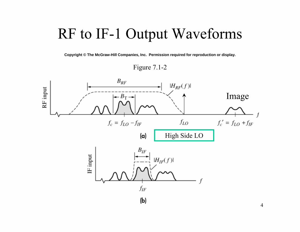
Copyright © The McGraw-Hill Companies, Inc. Permission required for reproduction or display.
Figure 7.1-2
RF to IF-1 Output Waveforms
Image
High Side LO
Image Considerations
• Real mixing always places the signal of interest band and an image band into the IF bandwidth.
• To avoid interferences:– (1) Filter out energy in the image band before mixing– (2) Use a receiver technique that cancels or nulls energy
in the image band. (complex or quadrature mixing)
5
6
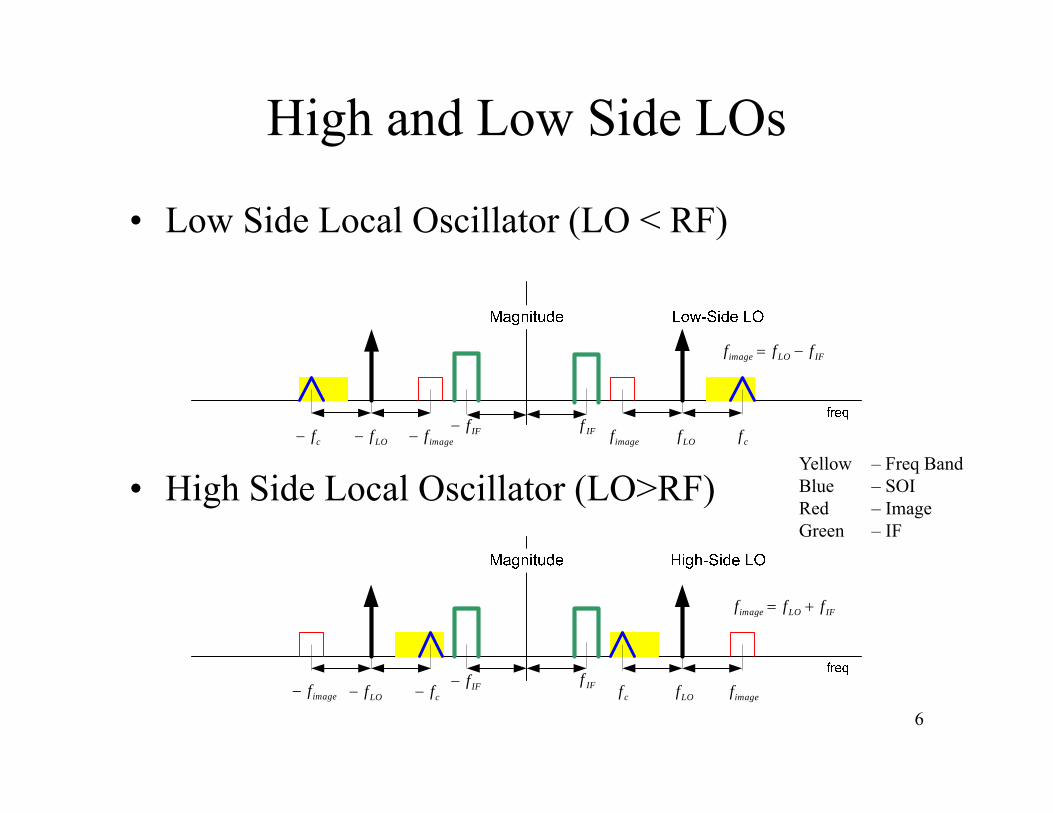
High and Low Side LOs
• Low Side Local Oscillator (LO < RF)
• High Side Local Oscillator (LO>RF)
LOfcfIFf
imagefIFfLOf cfimagef
IFLOimage fff
LOf cfIFf
imagefIFfLOfcf imagef
IFLOimage fff
Yellow – Freq BandBlue – SOIRed – ImageGreen – IF
7
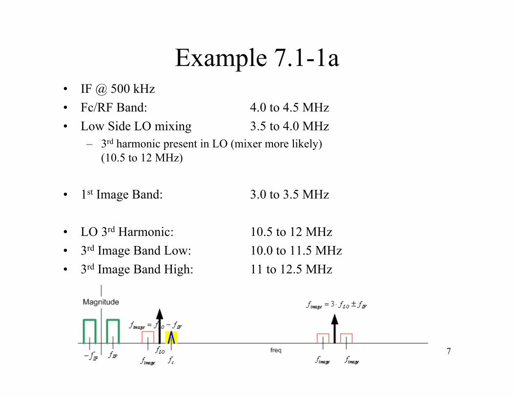
Example 7.1-1a• IF @ 500 kHz• Fc/RF Band: 4.0 to 4.5 MHz• Low Side LO mixing 3.5 to 4.0 MHz
– 3rd harmonic present in LO (mixer more likely)(10.5 to 12 MHz)
• 1st Image Band: 3.0 to 3.5 MHz
• LO 3rd Harmonic: 10.5 to 12 MHz• 3rd Image Band Low: 10.0 to 11.5 MHz• 3rd Image Band High: 11 to 12.5 MHz

8
Example 7.1-1b• IF @ 500 kHz• Fc/RF Band: 4.0 to 4.5 MHz• High Side LO Mixing 4.5 to 5.0 MHz• 3rd harmonic present in LO (mixer more likely)
– (13.5 to 15 MHz)
• 1st Image Band: 3.5 to 4.0 MHz
• LO 3rd Harmonic: 13.5 to 15MHz• 3rd Image Band Low: 13.0 to 14.5 MHz• 3rd Image Band High: 14 to 15.5 MHz
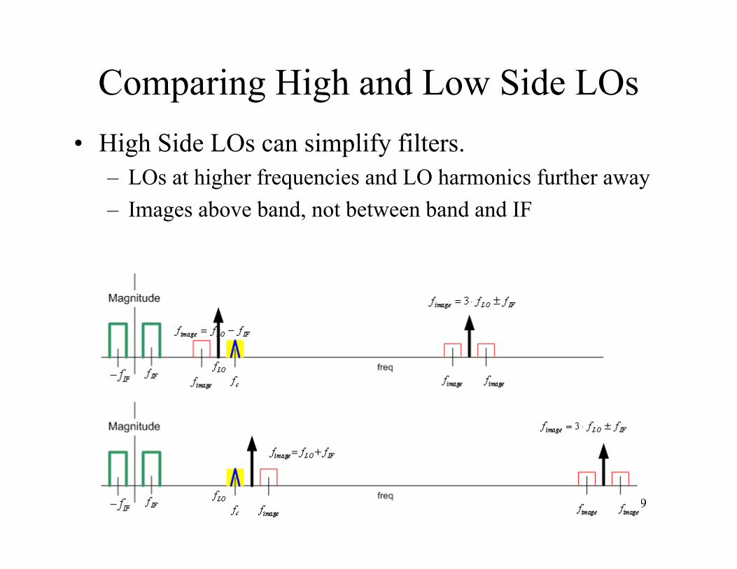
Comparing High and Low Side LOs• High Side LOs can simplify filters.
– LOs at higher frequencies and LO harmonics further away– Images above band, not between band and IF
9
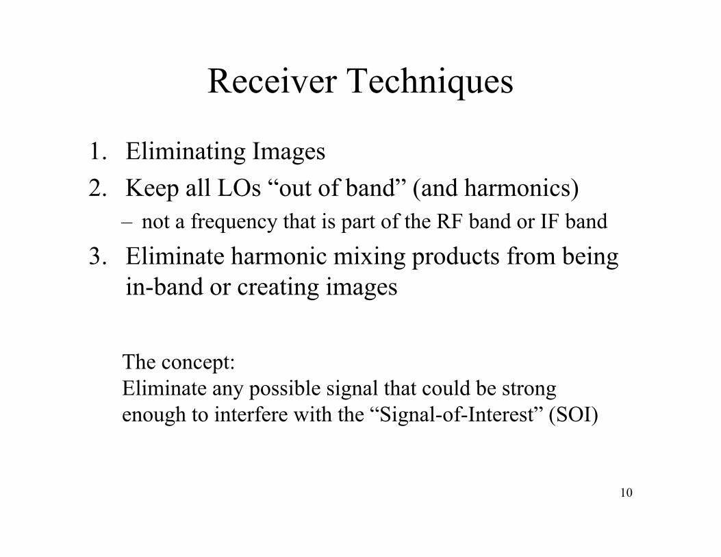
Receiver Techniques
1. Eliminating Images2. Keep all LOs “out of band” (and harmonics)
– not a frequency that is part of the RF band or IF band
3. Eliminate harmonic mixing products from being in-band or creating images
10
The concept:Eliminate any possible signal that could be strong enough to interfere with the “Signal-of-Interest” (SOI)
11
Copyright © The McGraw-Hill Companies, Inc. Permission required for reproduction or display.
Figure 7.1-3
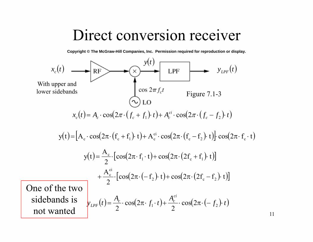
Direct conversion receiver
tf2costff2cosAtff2cosAty c2ccic1cc
tff22costf2cos2
A
tff22costf2cos2
Aty
2c2
cic
1c1c
tffAtffAtx ccicccc 21 2cos2cos
tfAtfAtycicc
LPF 21 2cos2
2cos2
One of the two sidebands is not wanted
txc
With upper and lower sidebands
ty tyLPF

Direct conversion receiver with opposite sideband (image) rejection
12Copyright © The McGraw-Hill Companies, Inc. Permission required
for reproduction or display.
Figure 7.1-4
Image Cancellation
13
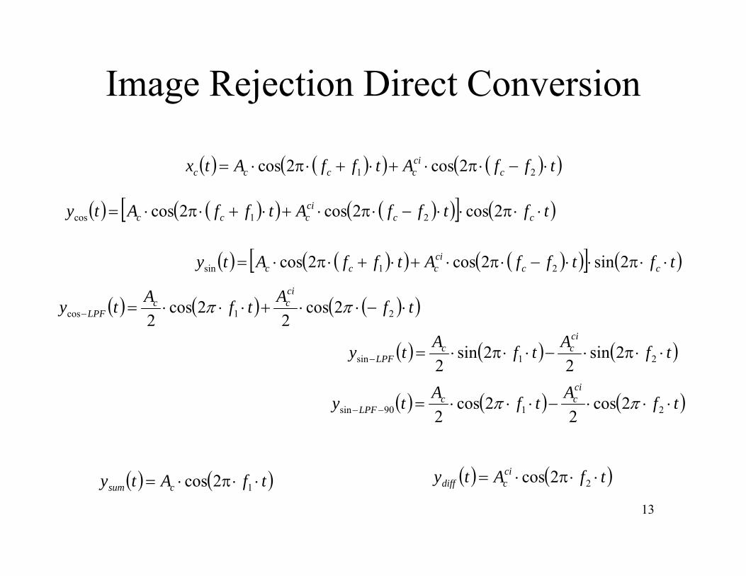
Image Rejection Direct Conversion
tftffAtffAty ccciccc 2cos2cos2cos 21cos
tfAtfAtycicc
LPF 21cos 2cos2
2cos2
tffAtffAtx ccicccc 21 2cos2cos
tfAty csum 12cos
tftffAtffAty ccciccc 2sin2cos2cos 21sin
tfAtfAtycicc
LPF 21sin 2sin2
2sin2
tfAtfAtycicc
LPF 2190sin 2cos2
2cos2
tfAty cicdiff 22cos
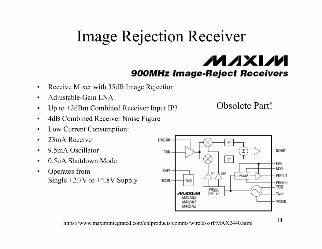
Image Rejection Receiver
• Receive Mixer with 35dB Image Rejection• Adjustable-Gain LNA• Up to +2dBm Combined Receiver Input IP3• 4dB Combined Receiver Noise Figure• Low Current Consumption:• 23mA Receive• 9.5mA Oscillator• 0.5μA Shutdown Mode• Operates from
Single +2.7V to +4.8V Supply
14https://www.maximintegrated.com/en/products/comms/wireless-rf/MAX2440.html
Obsolete Part!

15
Copyright © The McGraw-Hill Companies, Inc. Permission required for reproduction or display.
Figure 7.1-5
Double conversion receiver
Dual Conversion Superhet, typically using high side LOs
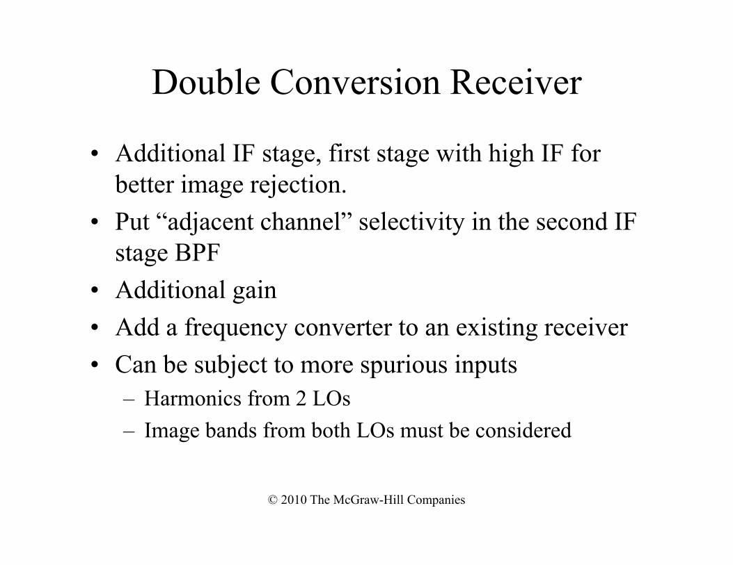
Double Conversion Receiver
• Additional IF stage, first stage with high IF for better image rejection.
• Put “adjacent channel” selectivity in the second IF stage BPF
• Additional gain• Add a frequency converter to an existing receiver• Can be subject to more spurious inputs
– Harmonics from 2 LOs– Image bands from both LOs must be considered
© 2010 The McGraw-Hill Companies
17
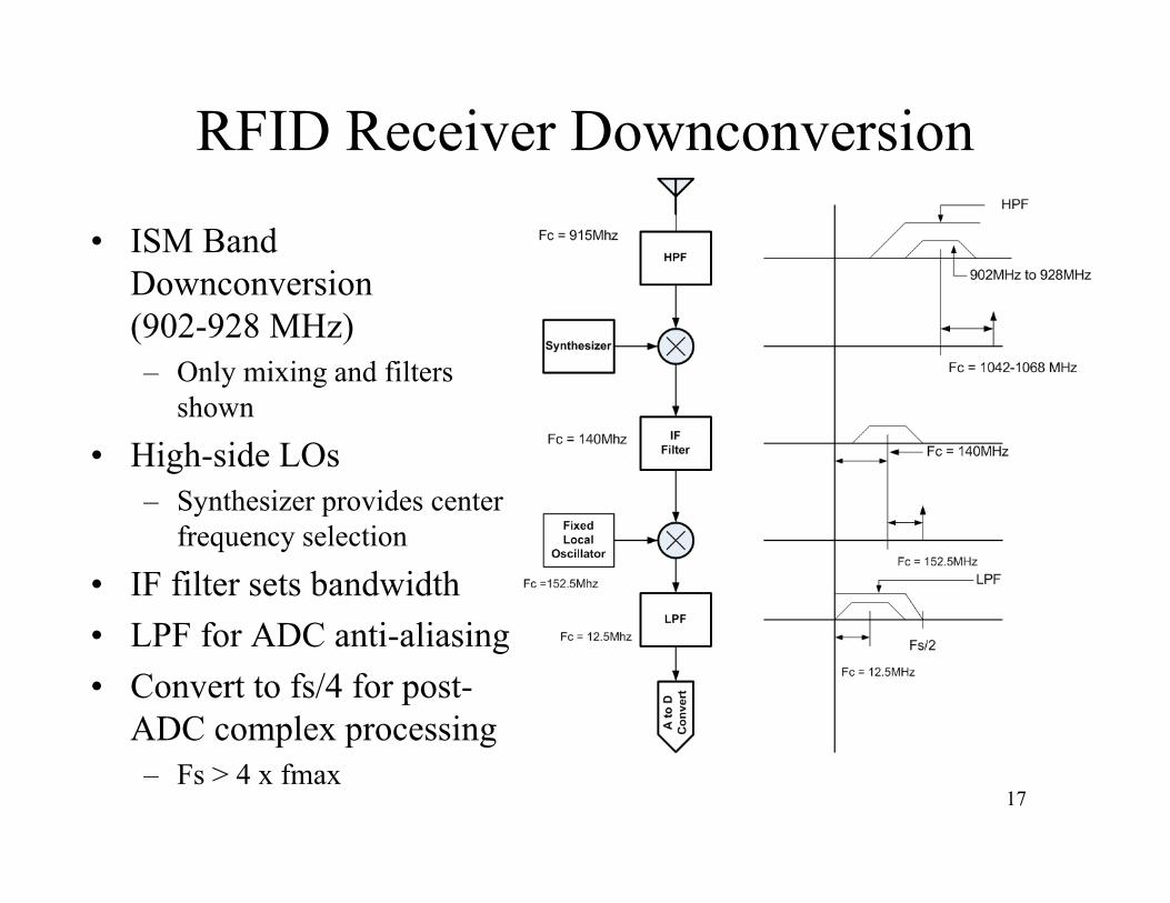
RFID Receiver Downconversion
• ISM Band Downconversion (902-928 MHz)– Only mixing and filters
shown
• High-side LOs– Synthesizer provides center
frequency selection
• IF filter sets bandwidth• LPF for ADC anti-aliasing• Convert to fs/4 for post-
ADC complex processing– Fs > 4 x fmax
18
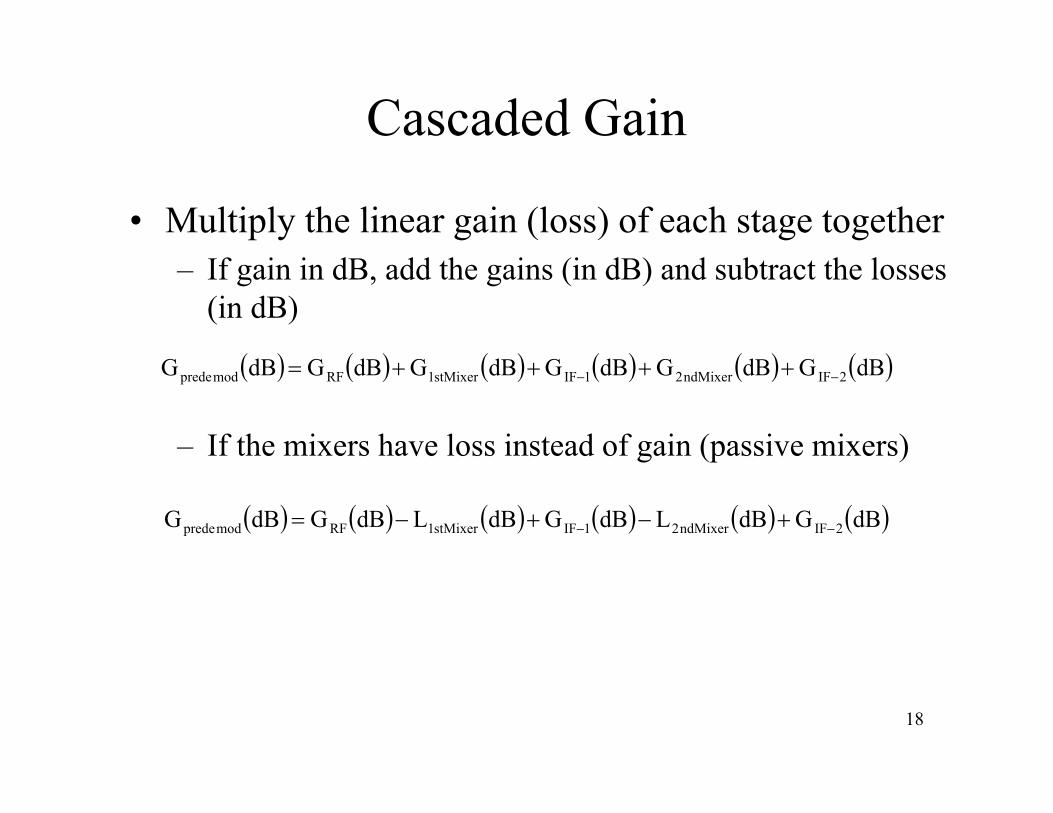
Cascaded Gain
• Multiply the linear gain (loss) of each stage together– If gain in dB, add the gains (in dB) and subtract the losses
(in dB)
– If the mixers have loss instead of gain (passive mixers)
dBGdBGdBGdBGdBGdBG 2IFndMixer21IFstMixer1RFmodprede
dBGdBLdBGdBLdBGdBG 2IFndMixer21IFstMixer1RFmodprede
19
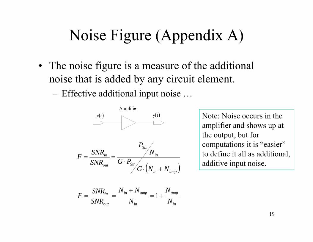
Noise Figure (Appendix A)
• The noise figure is a measure of the additional noise that is added by any circuit element.– Effective additional input noise …
ampin
Sin
in
Sin
out
in
NNGPG
NP
SNRSNRF
tx ty
in
amp
in
ampin
out
in
NN
NNN
SNRSNRF
1
Note: Noise occurs in the amplifier and shows up at the output, but for computations it is “easier” to define it all as additional, additive input noise.
20
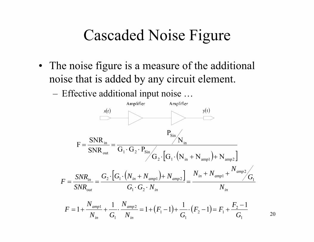
Cascaded Noise Figure
• The noise figure is a measure of the additional noise that is added by any circuit element.– Effective additional input noise …
1
212
11
2
1
1 1111111G
FFFG
FN
NGN
NF
in
amp
in
amp
2amp1ampin12
Sin21
in
Sin
out
in
NNNGGPGG
NP
SNRSNRF
tx ty
in
ampampin
in
ampampin
out
in
NG
NNN
NGGNNNGG
SNRSNRF 1
21
21
2112
21
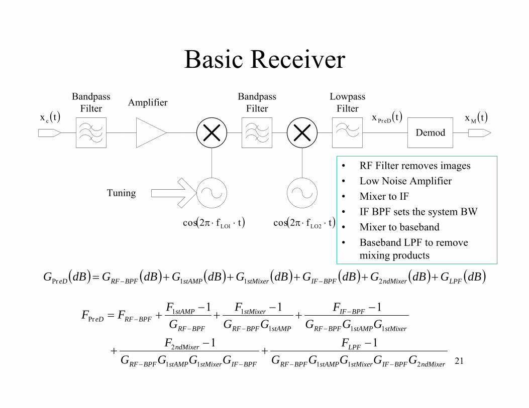
Basic Receiver
• RF Filter removes images• Low Noise Amplifier• Mixer to IF• IF BPF sets the system BW• Mixer to baseband• Baseband LPF to remove
mixing products
dBGdBGdBGdBGdBGdBGdBG LPFndMixerBPFIFstMixerstAMPBPFRFeD 211Pr
ndMixerBPFIFstMixerstAMPBPFRF
LPF
BPFIFstMixerstAMPBPFRF
ndMixer
stMixerstAMPBPFRF
BPFIF
stAMPBPFRF
stMixer
BPFRF
stAMPBPFRFeD
GGGGGF
GGGGF
GGGF
GGF
GFFF
21111
2
111
11Pr
11
111
tf2cos 1LO
tx c
Bandpass Filter
tf2cos 2LO
tx M
Amplifier Lowpass Filter
Demod
Bandpass Filter
Tuning
tx eDPr
22
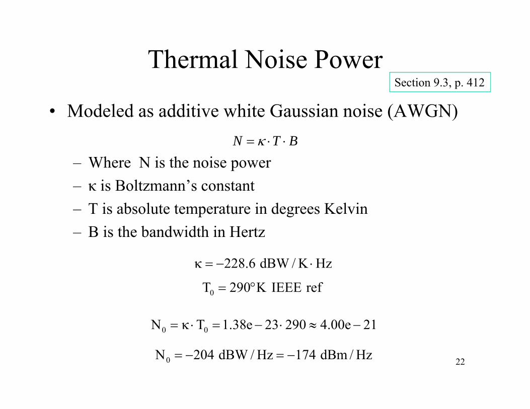
Thermal Noise Power
• Modeled as additive white Gaussian noise (AWGN)
– Where N is the noise power– κ is Boltzmann’s constant– T is absolute temperature in degrees Kelvin– B is the bandwidth in Hertz
BTN
HzK/dBW6.228
refIEEEK290T0
21e00.429023e38.1TN 00
Hz/dBm174Hz/dBW204N0
Section 9.3, p. 412

23
Receiver Operating Characteristics
• Sensitivity – minimum input value• Dynamic Range – usable signal range • Selectivity – filter out adjacent noise and
interference• Adjacent Channel Interference (ACI) Rejection
and Image Rejection• Noise Figure
Building a performance diagram for a software radio
RF Input to ADC input
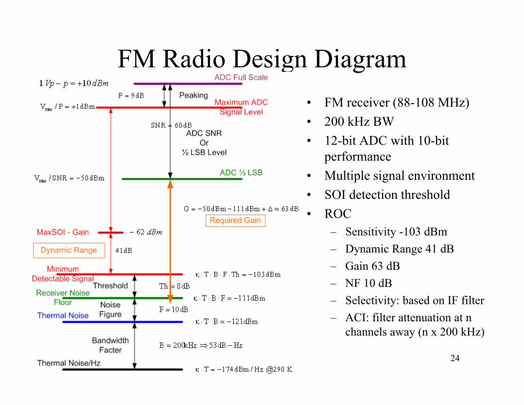
24
FM Radio Design Diagram• FM receiver (88-108 MHz)• 200 kHz BW• 12-bit ADC with 10-bit
performance• Multiple signal environment• SOI detection threshold• ROC
– Sensitivity -103 dBm– Dynamic Range 41 dB– Gain 63 dB– NF 10 dB– Selectivity: based on IF filter– ACI: filter attenuation at n
channels away (n x 200 kHz)

25
Copyright © The McGraw-Hill Companies, Inc. Permission required for reproduction or display.
Scanning Spectrum Analyzer
a) block diagram (b) amplitude responseFigure 7.1-6

26
Spectrum Analyzer Considerations
• Resolution Bandwidth – The bandwidth of the signal power measurement– Change it and the noise power must change!– IF Filter setting defines the RB
• Video Bandwidth – The filter prior to displaying the scan on the screen– Baseband filter setting
• Sweep time must support the filters!– typically adjusts with changes in RB
27
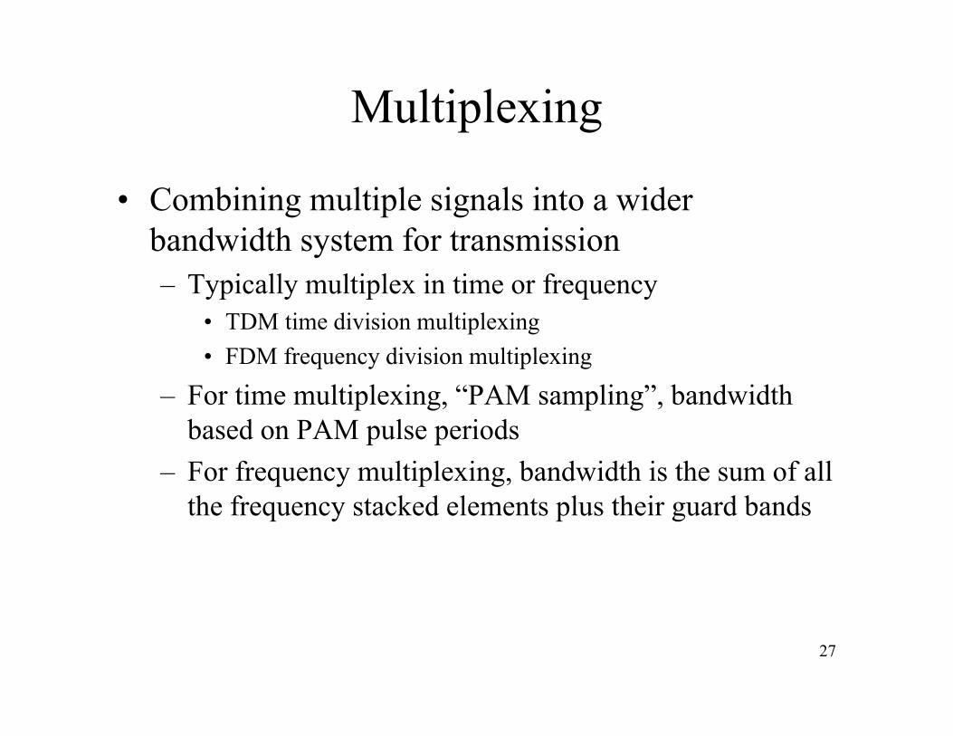
Multiplexing
• Combining multiple signals into a wider bandwidth system for transmission– Typically multiplex in time or frequency
• TDM time division multiplexing• FDM frequency division multiplexing
– For time multiplexing, “PAM sampling”, bandwidth based on PAM pulse periods
– For frequency multiplexing, bandwidth is the sum of all the frequency stacked elements plus their guard bands
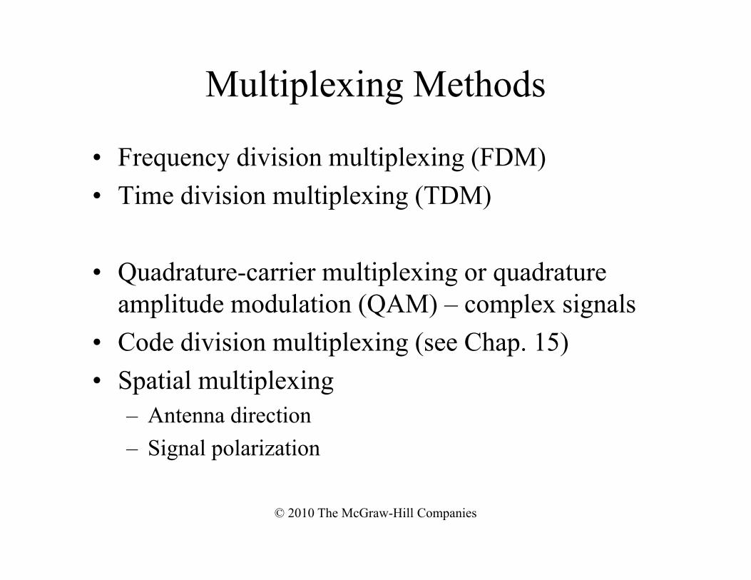
Multiplexing Methods
• Frequency division multiplexing (FDM)• Time division multiplexing (TDM)
• Quadrature-carrier multiplexing or quadrature amplitude modulation (QAM) – complex signals
• Code division multiplexing (see Chap. 15)• Spatial multiplexing
– Antenna direction– Signal polarization
© 2010 The McGraw-Hill Companies
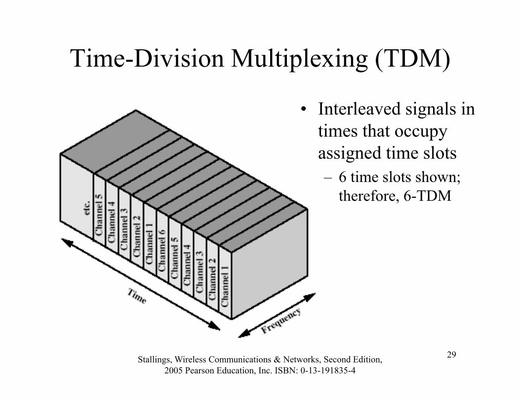
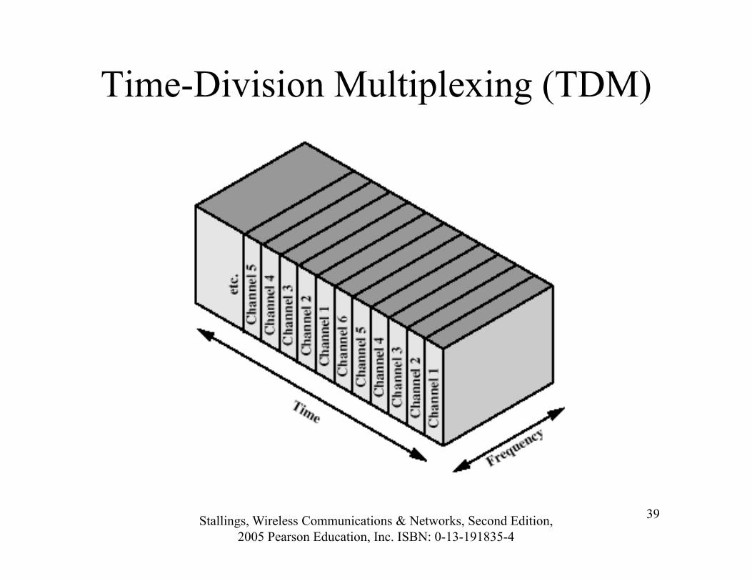
Time-Division Multiplexing (TDM)
29Stallings, Wireless Communications & Networks, Second Edition, 2005 Pearson Education, Inc. ISBN: 0-13-191835-4
• Interleaved signals in times that occupy assigned time slots– 6 time slots shown;
therefore, 6-TDM

Frequency-Division Multiplexing (FDM)
30Stallings, Wireless Communications & Networks, Second Edition, 2005 Pearson Education, Inc. ISBN: 0-13-191835-4
• Signal frequency bands stacked together, but transmitted as one wider bandwidth signal– 6 frequency bands
shown– Similar to 6 adjacent
radio stations using one transmitter
31
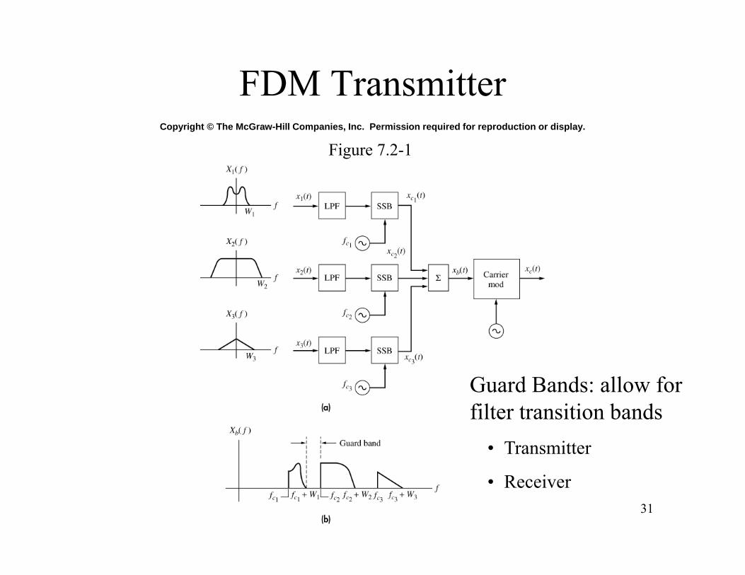
Copyright © The McGraw-Hill Companies, Inc. Permission required for reproduction or display.
Figure 7.2-1
FDM Transmitter
Guard Bands: allow for filter transition bands
• Transmitter
• Receiver
32
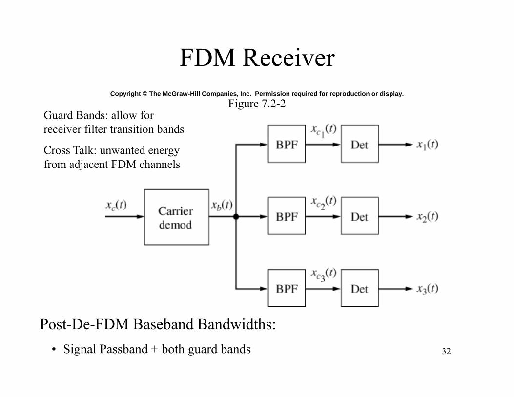
Copyright © The McGraw-Hill Companies, Inc. Permission required for reproduction or display.Figure 7.2-2
FDM Receiver
Guard Bands: allow for receiver filter transition bands
Cross Talk: unwanted energy from adjacent FDM channels
Post-De-FDM Baseband Bandwidths:• Signal Passband + both guard bands
33
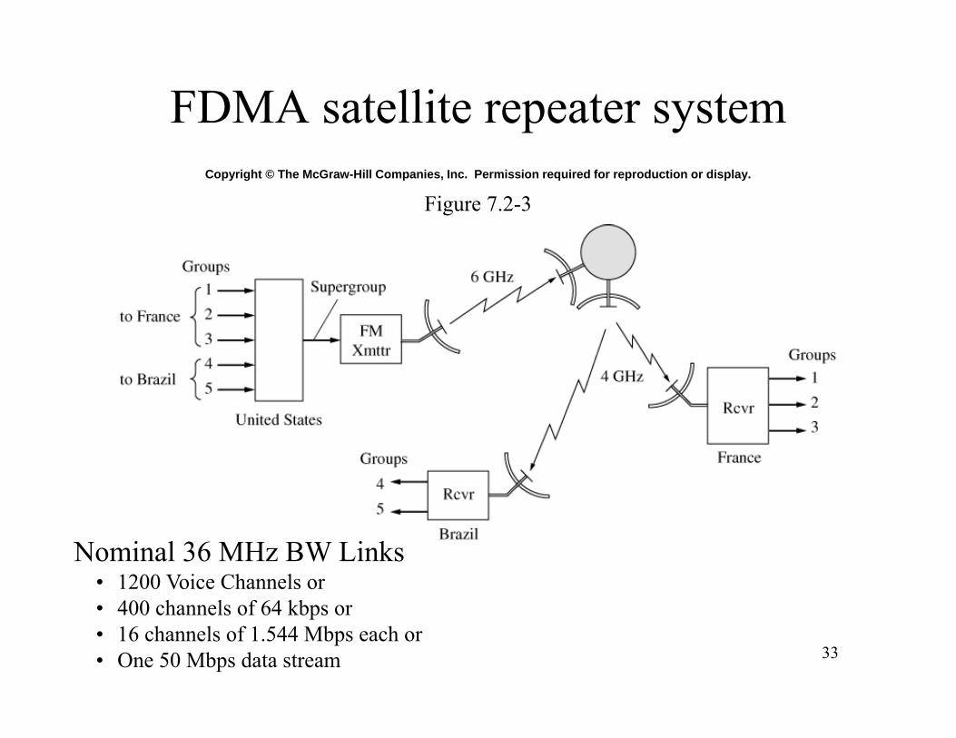
Copyright © The McGraw-Hill Companies, Inc. Permission required for reproduction or display.
Figure 7.2-3
FDMA satellite repeater system
Nominal 36 MHz BW Links• 1200 Voice Channels or• 400 channels of 64 kbps or• 16 channels of 1.544 Mbps each or• One 50 Mbps data stream

34
Copyright © The McGraw-Hill Companies, Inc. Permission required for reproduction or display.
(a) transmitter (b) baseband spectrumFigure 7.2-4
FM stereo multiplexing
FDM-FM• FDM baseband
• FM Signal
kHzBRF 250
MHzfMHz C 10888

35
Copyright © The McGraw-Hill Companies, Inc. Permission required for reproduction or display.
Figure 7.2-5
FM stereo multiplex receiver
See problems 6.1-4 & 6.1-5
kHzBIF 250
36
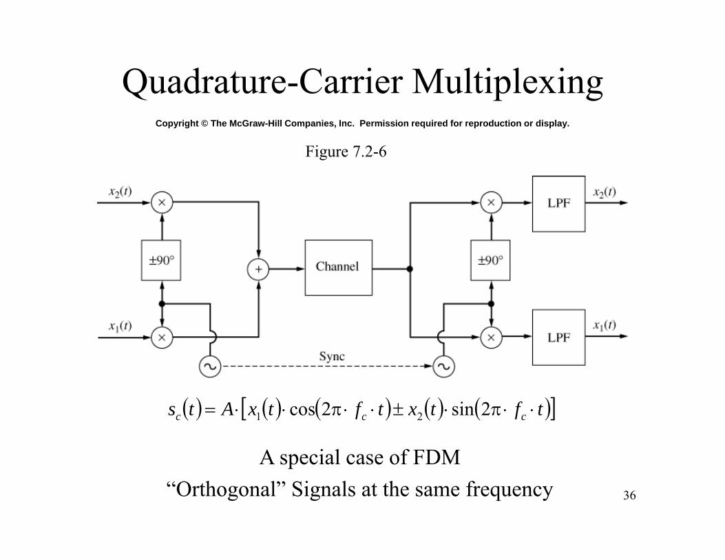
Copyright © The McGraw-Hill Companies, Inc. Permission required for reproduction or display.
Figure 7.2-6
Quadrature-Carrier Multiplexing
tftxtftxAts ccc 2sin2cos 21
A special case of FDM“Orthogonal” Signals at the same frequency
37
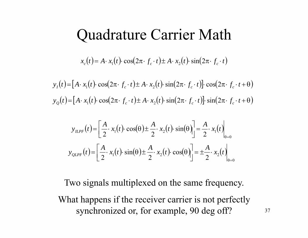
Quadrature Carrier Math
tftftxAtftxAty cccI 2cos2sin2cos 21
tftxAtftxAtx ccc 2sin2cos 21
tftftxAtftxAty cccQ 2sin2sin2cos 21
0
121 2sin
2cos
2
txAtxAtxAtyILPF
0
221 2cos
2sin
2
txAtxAtxAtyQLPF
Two signals multiplexed on the same frequency.
What happens if the receiver carrier is not perfectly synchronized or, for example, 90 deg off?
38
Quadrature FDM Channels
• Each of the frequency bands or channels may have signal that are in quadrature. – Doubling the channel capacity– Phase synchronization of the receiver with the received
waveform is required!
– A precursor to Orthogonal Frequency Division Multiplexing (OFDM)
39
Time-Division Multiplexing (TDM)
Stallings, Wireless Communications & Networks, Second Edition, 2005 Pearson Education, Inc. ISBN: 0-13-191835-4
40
Copyright © The McGraw-Hill Companies, Inc. Permission required for reproduction or display.
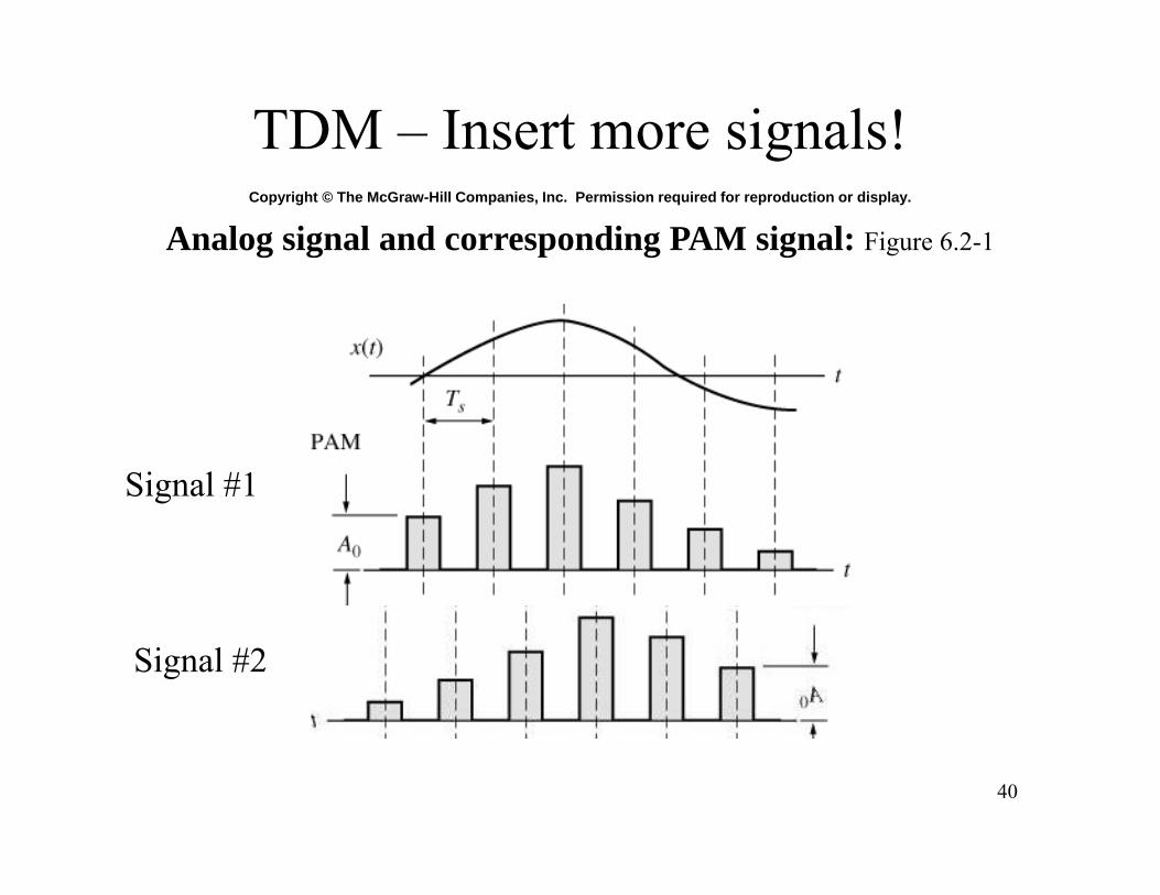
Analog signal and corresponding PAM signal: Figure 6.2-1
TDM – Insert more signals!
Signal #1
Signal #2

41
Copyright © The McGraw-Hill Companies, Inc. Permission required for reproduction or display.
(a) block diagram (b) waveformsFigure 7.2-7
TDM system
PAM inputs multiplexed in time
PAM outputs for reconstruction
42
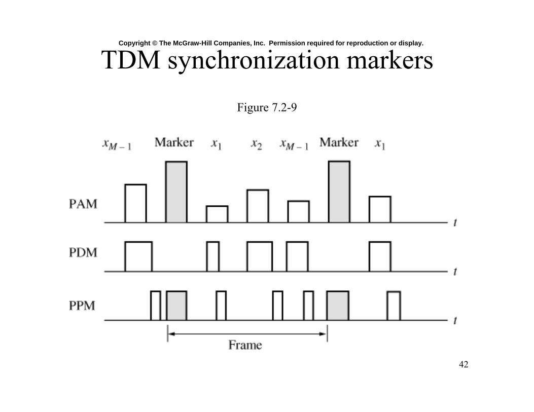
Copyright © The McGraw-Hill Companies, Inc. Permission required for reproduction or display.
Figure 7.2-9
TDM synchronization markers

43
Copyright © The McGraw-Hill Companies, Inc. Permission required for reproduction or display.
(a) TDM transmitter with baseband filtering (b) baseband waveformFigure 7.2-10
TDM Continuous Transmitter

44
Copyright © The McGraw-Hill Companies, Inc. Permission required for reproduction or display.
Cross talk in TDM
Sufficient time must be available for the receiver to transition from one PAM level to the next. Otherwise adjacent signals effect each other – defined as cross talk.
dBinTBAAk g
ctct
5.54log10 10
Guard time
B = 3dB Bandwidth
gct TBAA 2exp
Figure 7.2-12
B = 3dB Bandwidth

TDM/PPM with guard time
• Time-division-multiplexing multiple pulse-position-modulated signals.– Pulse center +/- t0
45
time
2
0t 0t
gT
MTs
0t2 gT
0t

2
2
0t 0t
gT
MTs
46
TDM/PPM with guard time
Forward and backward maximum locations, t0
22 00
tTtMT
gs
g
s TMTt
21
0
4th ed. Figure 7.2-13 is wrong: Fix - Tg is between the signal pulses
5th ed. Figure 7.2-13 is wrong: to is on opposite side of pulses

47
Comparing TDM and FDM
• TDM based on time slots– Overlap in frequency domain– Bandwidth of total signal defines cross talk– Well supported by digital circuitry, multiple mux rates– Synchronization concerns– Time based receiver, therefore less dependent upon
filter performance or ripple
• FDM based on frequency slots– Overlap in time domain– Guard bands and filtering determine cross talk– Simple frequency assignments
48
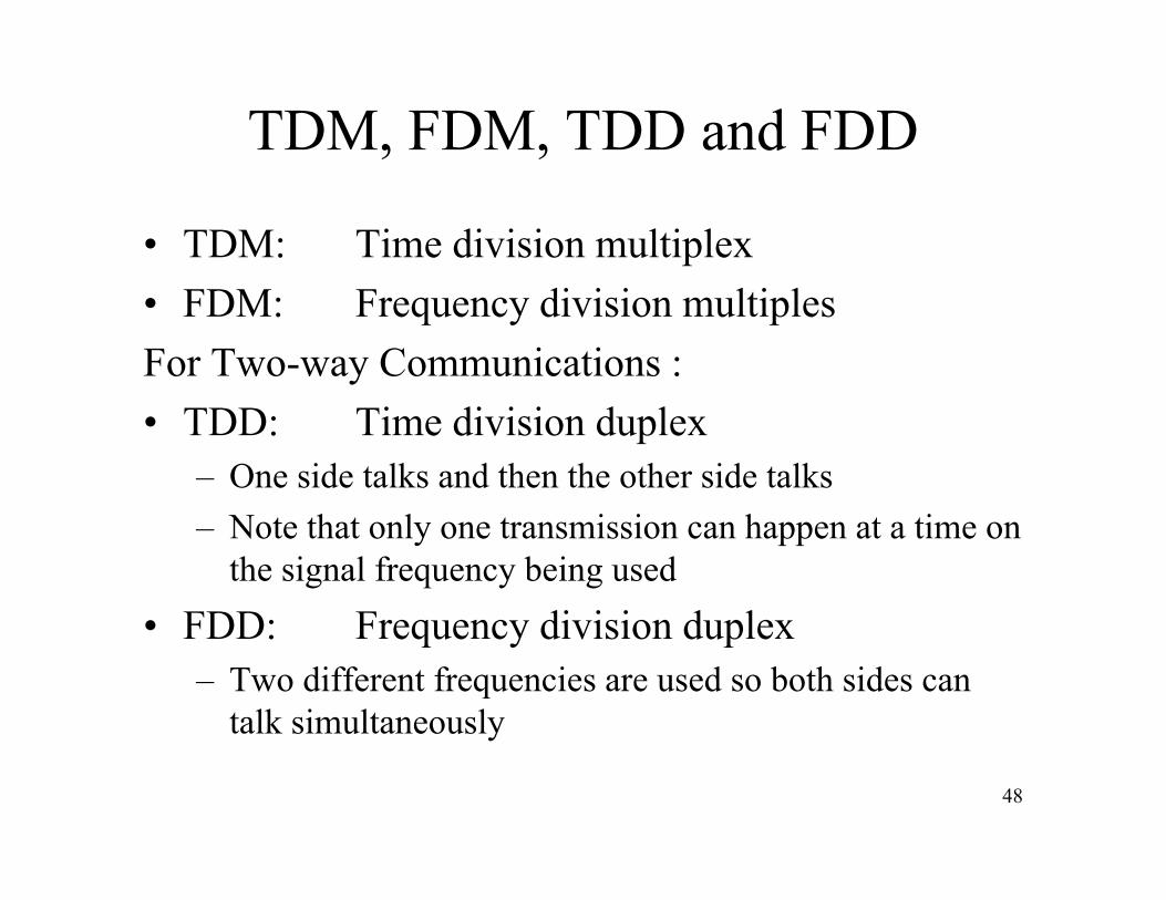
TDM, FDM, TDD and FDD
• TDM: Time division multiplex• FDM: Frequency division multiplesFor Two-way Communications :• TDD: Time division duplex
– One side talks and then the other side talks– Note that only one transmission can happen at a time on
the signal frequency being used
• FDD: Frequency division duplex– Two different frequencies are used so both sides can
talk simultaneously


![Communication Systems, 5ebazuinb/ECE4600/Ch02_3.pdf · 2020. 9. 9. · Inverse DFT ( ) IDFT[ ( )] 1 ( ) ( ) 0,1,... 1 N jnkN n x kXn xk X ne n N N ... Circular convolution both functions](https://img.pdfslide.net/doc/110x75/60daad6fab0da1213449dd88/communication-systems-5e-bazuinbece4600ch023pdf-2020-9-9-inverse-dft.jpg)