Embed Size (px)
Citation preview

COMPARISON OF CLASSICAL AND CHARGE STORAGE METHODS FOR DETERMINING CONDUCTIVITY OF THIN FILM INSULATORS
Prasanna Swaminathan
Physics Department, Utah State University Logan, UT, USA 84322-4415
Phone: (435) 797-2936 Fax: (435) 797-2492
E-mail: [email protected]
J.R. Dennison Alec Sim
Jerilyn Brunson Eric Crapo
Physics Department, Utah State University
A. R. Frederickson Caltech Jet Propulsion Laboratory
Abstract
Conductivity of insulating materials is a key parameter to determine how accumulated charge
will distribute across the spacecraft and how rapidly charge imbalance will dissipate. Classical ASTM and IEC methods to measure thin film insulator conductivity apply a constant voltage to two electrodes around the sample and measure the resulting current for tens of minutes. However, conductivity is more appropriately measured for spacecraft charging applications as the "decay" of charge deposited on the surface of an insulator. Charge decay methods expose one side of the insulator in vacuum to sequences of charged particles, light, and plasma, with a metal electrode attached to the other side of the insulator. Data are obtained by capacitive coupling to measure both the resulting voltage on the open surface and emission of electrons from the exposed surface, as well monitoring currents to the electrode. Instrumentation for both classical and charge storage decay methods has been developed and tested at Jet Propulsion Laboratory (JPL) and at Utah State University (USU). Details of the apparatus, test methods and data analysis are given here. The JPL charge storage decay chamber is a first-generation instrument, designed to make detailed measurements on only three to five samples at a time. Because samples must typically be tested for over a month, a second-generation high sample throughput charge storage decay chamber was developed at USU with the capability of testing up to 32 samples simultaneously. Details are provided about the instrumentation to measure surface charge and current; for charge deposition apparatus and control; the sample holders to properly isolate the mounted samples; the sample carousel to rotate samples into place; the control of the sample environment including sample vacuum, ambient gas, and sample temperature; and the computer control and data acquisition systems. Measurements are compared here for a number of thin film insulators using both methods at both facilities. We have found that conductivity determined from charge storage decay methods is 102 to 104 larger than values obtained from classical methods. Another Spacecraft Charging Conference presentation describes more extensive measurements made with these apparatus. This work is supported through funding from the NASA Space Environments and Effects Program and the USU Space Dynamics Laboratory Enabling Technologies Program.
https://ntrs.nasa.gov/search.jsp?R=20040111057 2020-04-27T19:24:45+00:00Z

Introduction
As interaction with the space environment builds up charge on spacecraft surfaces, the rate at which further charge accumulates will be affected. In the simplest scenario, for a fully conductive spacecraft the charge will readily redistribute over the entire satellite and will charge to the point where the incident currents from the environment fluxes are equal to emission currents. By contrast, as insulating spacecraft materials accumulate charge, their low charge mobility causes that charge to accumulate where deposited and local electric fields to rise until the leakage current from the insulators to conductors equals the accumulation current from the environment (or until the insulator actually breaks down and generates a charge pulse). Hence, conductivity of insulating materials is a key parameter to determine how accumulated charge will distribute across the spacecraft, how rapidly charge imbalance will dissipate, and what equilibrium potential an insulator will adopt under given environmental conditions [1].
Determination of values of resistivity for typical thin film insulating materials applicable to service in the space environment is problematic [1,2,3,4]. The bulk resistivity values of insulators used to model spacecraft charging have traditionally been obtained from the handbook [5] values found by the classical ASTM/IEC methods [6,7]. Classical methods use a parallel plate capacitor configuration to determine the conductivity of insulators by application of a constant voltage (E field) and the measurement of the resulting leakage current across the plates and through the insulator [6].
However, recent works have shown that these classical methods are often not applicable to situations encountered in spacecraft charging [1,2,3,4]. Conductivity is more appropriately measured for spacecraft charging applications as the "decay" of charge deposited on the surface of an insulator. Charge decay methods expose one side of the insulator in vacuum to sequences of charged particles, light, and plasma, with a metal electrode attached to the other side of the insulator. Data are obtained by capacitive coupling to measure both the resulting voltage on the open surface and emission of electrons from the exposed surface, as well monitoring currents to the electrode. When the resistivity data obtained were compared to existing ASTM data for some spacecraft insulators, the data calculated by the ASTM method was found to be higher by up to four orders of magnitude [1,2,3,4]. Results of the charge storage method have already been shown to correctly predict charging events observed in real satellite data, through modeling of pulses occurring aboard the CRESS satellite [4].
Given these results, we have concluded that classical resistivity methods are not the most appropriate methods for many spacecraft charging problems. Specifically,
1. The charge injection methods, and resulting internal charge profile and E field, are
fundamentally different for the classical and charge storage methods. The voltages developed in space are generated by impressing charge into the insulation, not by the application of voltage from a power supply onto electrodes.
2. Conductors are placed on both surfaces of the insulators in ASTM tests, whereas the spacecraft
most often has only one surface of the insulator in contact with a conductor.

3. The ASTM methods use classical ground conditions and are basically designed for the problems associated with power loss through the dielectric and not how long charge can be stored on an insulator surface or in the insulator interior [6].
4. The measurement of the leakage current is made only after few minutes of bias application in
the classical methods. Initial measurements by Frederickson at the JPL indicate that the resistivity changes with time and that to adequately characterize the change of resistance with time, requires monitoring stored charge for up to 1 month [1,2,3,4]. The resistivity data in handbooks do not take into consideration the fact that the resistivity continues to increase even after the measurement is taken. But in spacecraft modeling we need to know the how the leakage decays for as long as year or more [1,2].
This paper describes the instrumentation and methods developed to implement the charge
storage measurements and compares preliminary results of this effort with classical resistivity measurements. The work is a joint project by the Jet Propulsion Laboratory (JPL) and Utah State University (USU) sponsored through the NASA Space Environments and Effects (SEE) Program [8]. Preliminary studies using the charge storage method and further details of the methods and instrumentation are found elsewhere [1,2,3,4]. Classical Resistivity
Method
The classical method for measuring the resistivity of thin film insulators is based upon measuring current flowing through a well-defined sample structure, for which the relationship between the material’s resistivity and the sample’s resistance can be determined [6,7]. Figure 1(a) shows the preferred sample design for the ASTM-IEC or capacitor resistance method that is valid in the range of 107<ρ<1021 Ω·cm. An adjustable high voltage is applied to one sample electrode. Current flow to the sample electrode held at ground is measured by a picoammeter. A grounded guard ring serves to help establish approximately parallel electric field lines of uniform magnitude and to define the volume of material in which the measured current flows [6]. The resistance of the sample is then given by effAdR /ρ= , where ρ is the resistivity (ohm-cm), Aeff is the effective area (cm2) slightly larger than the metal electrode, and d (cm) is the sample thickness. The resistance R is determined from an I-V curve using Ohm’s law.
(a) (b) Figure 1. (a) Preferred sample design for classical resistivity
method for thin insulators. (b) Experimental setup ofclassical method at JPL.
Classical resistivity measurements can vary appreciably—from factors of two to two orders of
magnitude—due to variations in sample environments and test conditions [6]. Most reported ρ values are derived from measurements made at ambient temperature and relative humidity, which is not representative of the wide temperature range and vacuum conditions in which space hardware operates. Temperature variations can often be described as Arrhenius behavior of the form ]/exp[ TkE BAoρρ = , where ρo is a material parameter and EA is an activation energy

characteristic of a particular energy absorption process. Resistivity also changes appreciably—often orders of magnitude—with relative humidity or moisture content, particularly for thin film samples. Both ambient humidity and drying during sample conditioning need to be considered [6,9]. For example, resistivity has been shown to vary with time to the ½ power, as water diffused into or out of the sample [9]. Up to two orders of magnitude increase in ρ have been observed during vacuum pump down of polymer films [9] Further, dielectric resistivity often depends on duration and magnitude of the applied sample voltage. The observed decrease in current with time is due primarily to dielectric absorption (e.g., interfacial polarization, volume charge, rearrangement of dipoles on the molecular level, etc.) and ion migration into the electrodes; it usually has the form I(t)=A·t-m, where 0<m<1. Excessive voltage produces high internal electric fields, resulting in breakdown of the insulator when the dielectric strength is exceeded (typically, when the field exceeds 105 kV/cm) [2]. Sample impurities or surface contamination are known to substantially affect bulk resistivity and surface resistivity, respectively. Given the substantial variability in resistivity from these factors, it is essential that the sample preparation, conditioning history, and environment be well characterized and controlled for such measurements.
Classical method instrumentation at JPL
The classical method of measurement of resisitivity of thin film insulators at JPL follows the ASTM-257-99 guidelines [6], as shown in Figure 1(b). A damp cardboard is used to make more complete contact on the open face of the sample. A positive 64 V is applied for ten minutes at the end of which the current is recorded [2]. The bias polarity is then reversed and after 10 minutes the current is recorded. The resistance is defined as the ratio between the change in voltage (128 volts) and the change in current. Figure 3 shows the classical resistivity measurement from JPL as a function of time for 51 µm thick sample at 64 V [2]. Classical method instrumentation at USU
(a) (b) Figure 2. Photographs of USU capacitor resistance
apparatus (CRA). (a) View of the CRA connected to the low voltage power supply and picoammeter. (b) Top view with lid removed showing the interior and copper braid from thermal reservoir to heat sink.
The capacitive resistance
apparatus (CRA) at USU is designed as a more versatile instrument for classical resistance measurements under more tightly controlled conditions (see Fig. 2). The sample environment—including sample temperature, ambient vacuum or background gas, and humidity—can be strictly controlled. Computer automation of voltage and current measurements, together with environmental parameters, allow rapid and prolonged resistance measurements. Thus, the apparatus is capable of parametric studies of variables

that influence the resistivity, including sample material and thickness, applied voltage magnitude and duration, sample temperature, ambient gas or vacuum, and humidity.
Two independent thin film insulator samples of up to ~1 mm thick can be mounted in the
apparatus simultaneously; these are stretched over an electrically and thermally isolated Cu high voltage electrode and held smoothly in place with two polycarbonate sample clamps each. An adjustable voltage is applied using either a 0 to ±110 VDC, a 0 to 1 keV, or a 0 V to ±50 keV computer-controlled power supply, depending on the range required. Wiring to the high voltage electrode uses corona-free high voltage Teflon-insulated wire to a standard 15 kV coaxial SHV vacuum feedthrough. Current flow through the samples to two independent sample inner electrodes held at ground is measured by a dual channel picoammeter [2]. The unit is also designed to measure the punchthrough voltage of thin insulating films, by monitoring current across the sample while applying up to ±15 keV across the sample electrodes [10].
The unit is designed to control the temperature of the electrodes and the sandwiched samples to
~ ±2 °C using a standard PID temperature controller and platinum resistance thermometers. Two 70 W thermoelectric Peltier cooling units are mounted above the sample electrodes. In cooling mode, the Peltier coolers are designed to cool the sample to –100 °C and exhaust excess heat via a copper braid to an external heat sink through a O-ring-sealed compression port. In heating mode, the Peltier coolers are run with reverse voltage, drawing heat from the external heat sink. In this mode, the unit is designed to heat the electrodes up to +100°C.
The CRA aluminum-walled vacuum chamber is pumped with the same system used for the
charge storage chamber (see details below). Ultimate pressure of the CRA system is 10-5 Torr, limited by pumping speed and O-ring seals. Vacuum connections between to the CRA chamber are made using standard Quick Connect and ConflatTM fittings. The CRA vacuum chamber is also connected to a stainless steel gas handling system to allow control of the ambient gas environment composition and pressure; pressure is monitored by a standard vacuum thermocouple gauge (1 atm to 1 mTorr), a capacitance manometer (100 to 0.1 Torr), and a high pressure Si strain gauge transducer [10+6 to 100 Torr]. Results of classical resistivity methods
Figure 3 shows data obtained using the classical ASTM resistance method shown in Fig.1(b). The JPL data are for a 51 µm thick Kapton H sample from Dupont taken at room temperature and high humidity with 64 V. The USU data were obtained for Sheldahl thermal control blanket material (51 µm and 130 µm thick Kapton H with 0.1 µm vapor deposited Al) at 26±2 °C in ambient room light at 30±5% ambient relative humidity with wet electrodes for a range of voltages from 300 V to 900 V. The samples were cleaned with isopropyl alcohol.
The curves showed linear behavior on a log-log plot with a slope of ~½ and converged to
~(3±1) ·10+16 Ω·cm at ~½ hr. The published resistivity value for Dupont Kapton HN is 1·1017 Ω·cm [11]. There is no clear dependence of the data on applied voltage or sample thickness at 1 hr. Possible sources of deviation between samples include temperature, effectiveness of the voltage contacts, and drying time of the contact.
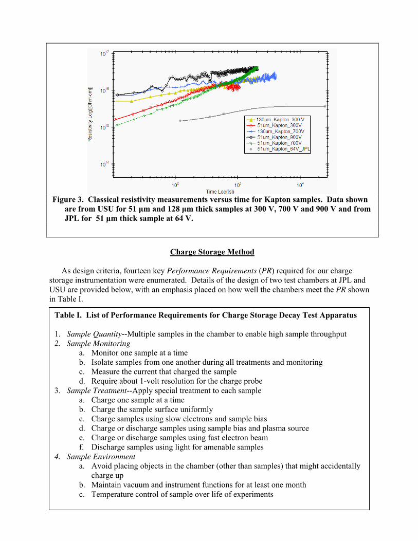
Figure 3. Classical resistivity measurements versus time for Kapton samples. Data shown
are from USU for 51 µm and 128 µm thick samples at 300 V, 700 V and 900 V and from JPL for 51 µm thick sample at 64 V.
Charge Storage Method
As design criteria, fourteen key Performance Requirements (PR) required for our charge storage instrumentation were enumerated. Details of the design of two test chambers at JPL and USU are provided below, with an emphasis placed on how well the chambers meet the PR shown in Table I.
Table I. List of Performance Requirements for Charge Storage Decay Test Apparatus 1. Sample Quantity--Multiple samples in the chamber to enable high sample throughput 2. Sample Monitoring
a. Monitor one sample at a time b. Isolate samples from one another during all treatments and monitoring c. Measure the current that charged the sample d. Require about 1-volt resolution for the charge probe
3. Sample Treatment--Apply special treatment to each sample a. Charge one sample at a time b. Charge the sample surface uniformly c. Charge samples using slow electrons and sample bias d. Charge or discharge samples using sample bias and plasma source e. Charge or discharge samples using fast electron beam f. Discharge samples using light for amenable samples
4. Sample Environment a. Avoid placing objects in the chamber (other than samples) that might accidentally
charge up b. Maintain vacuum and instrument functions for at least one month c. Temperature control of sample over life of experiments
Experimental setup of charge storage method at JPL
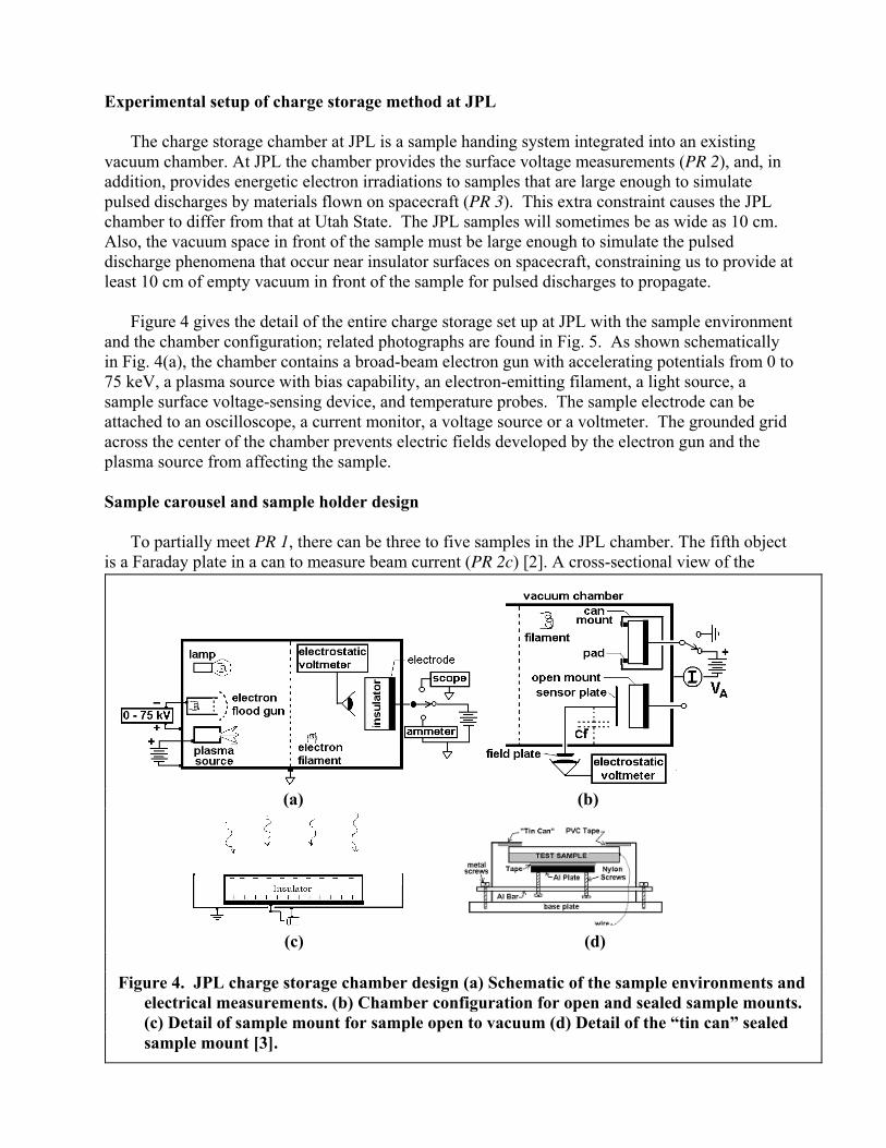
The charge storage chamber at JPL is a sample handing system integrated into an existing vacuum chamber. At JPL the chamber provides the surface voltage measurements (PR 2), and, in addition, provides energetic electron irradiations to samples that are large enough to simulate pulsed discharges by materials flown on spacecraft (PR 3). This extra constraint causes the JPL chamber to differ from that at Utah State. The JPL samples will sometimes be as wide as 10 cm. Also, the vacuum space in front of the sample must be large enough to simulate the pulsed discharge phenomena that occur near insulator surfaces on spacecraft, constraining us to provide at least 10 cm of empty vacuum in front of the sample for pulsed discharges to propagate.
Figure 4 gives the detail of the entire charge storage set up at JPL with the sample environment
and the chamber configuration; related photographs are found in Fig. 5. As shown schematically in Fig. 4(a), the chamber contains a broad-beam electron gun with accelerating potentials from 0 to 75 keV, a plasma source with bias capability, an electron-emitting filament, a light source, a sample surface voltage-sensing device, and temperature probes. The sample electrode can be attached to an oscilloscope, a current monitor, a voltage source or a voltmeter. The grounded grid across the center of the chamber prevents electric fields developed by the electron gun and the plasma source from affecting the sample.
Sample carousel and sample holder design
To partially meet PR 1, there can be three to five samples in the JPL chamber. The fifth object
is a Faraday plate in a can to measure beam current (PR 2c) [2]. A cross-sectional view of the
(a) (b)
Figure 4. JPL charge storage chamber design (a) Schematic of the sample environments and
electrical measurements. (b) Chamber configuration for open and sealed sample mounts. (c) Detail of sample mount for sample open to vacuum (d) Detail of the “tin can” sealed sample mount [3].
(d) (c)
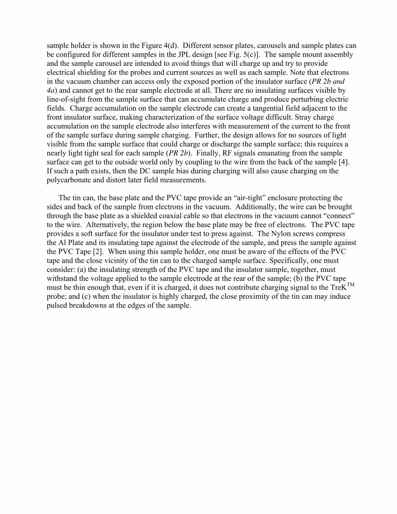
sample holder is shown in the Figure 4(d). Different sensor plates, carousels and sample plates can be configured for different samples in the JPL design [see Fig. 5(c)]. The sample mount assembly and the sample carousel are intended to avoid things that will charge up and try to provide electrical shielding for the probes and current sources as well as each sample. Note that electrons in the vacuum chamber can access only the exposed portion of the insulator surface (PR 2b and 4a) and cannot get to the rear sample electrode at all. There are no insulating surfaces visible by line-of-sight from the sample surface that can accumulate charge and produce perturbing electric fields. Charge accumulation on the sample electrode can create a tangential field adjacent to the front insulator surface, making characterization of the surface voltage difficult. Stray charge accumulation on the sample electrode also interferes with measurement of the current to the front of the sample surface during sample charging. Further, the design allows for no sources of light visible from the sample surface that could charge or discharge the sample surface; this requires a nearly light tight seal for each sample (PR 2b). Finally, RF signals emanating from the sample surface can get to the outside world only by coupling to the wire from the back of the sample [4]. If such a path exists, then the DC sample bias during charging will also cause charging on the polycarbonate and distort later field measurements.
The tin can, the base plate and the PVC tape provide an “air-tight” enclosure protecting the
sides and back of the sample from electrons in the vacuum. Additionally, the wire can be brought through the base plate as a shielded coaxial cable so that electrons in the vacuum cannot “connect” to the wire. Alternatively, the region below the base plate may be free of electrons. The PVC tape provides a soft surface for the insulator under test to press against. The Nylon screws compress the Al Plate and its insulating tape against the electrode of the sample, and press the sample against the PVC Tape [2]. When using this sample holder, one must be aware of the effects of the PVC tape and the close vicinity of the tin can to the charged sample surface. Specifically, one must consider: (a) the insulating strength of the PVC tape and the insulator sample, together, must withstand the voltage applied to the sample electrode at the rear of the sample; (b) the PVC tape must be thin enough that, even if it is charged, it does not contribute charging signal to the TreKTM
probe; and (c) when the insulator is highly charged, the close proximity of the tin can may induce pulsed breakdowns at the edges of the sample.
(a)
(b)
2
1
3 4
5
(c)
Figure 5. (a) Internal design of JPL charge storage chamber. (b) Photograph showing JPL chamber with door closed. (c) Carousel mounted to the door of the vacuum chamber on left half; the body of the vacuum chamber on right. Five samples are on this carousel: clockwise from 1-O’clock: (1) a square sample of circuit board material in the fully open mounting; (2) the mirror in the “air-tight” can; (3) and (4) two mirrors in an open configuration; and last (5) a carbon-coated metal in a can acting as a beam current monitor. When the door is closed, the carousel extends about 8 cm into the vacuum chamber and rubs against a carbon-coated aluminum plate called the shutter. The shutter is tightly affixed to the walls of the chamber.
(a) (b) (c)
(d) (e)
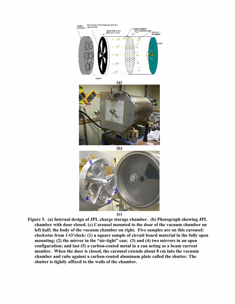
Figure 6. (a) Diagram of TreKTM probe dimensions. (b) Schematic of the TreKTM field probe and the sample configuration. (c) Details of the samples suspended across an opening in a thin aluminum plate with adhesive tape. (d) Structure of JPL can sample holder and field plate assembly inside the vacuum. The can covers the PLLA and its interior baffle. The grounded can does not contact the baffle nor the center screw that is connected to the sensor plate nor the PMMA. The second “baffle” and the stiff copper sensor wire are attached to the sensor plate screw and connect to the field plate via a short flexible clip lead and the center conductor of a BNC vacuum feed through. (e) One-inch copper field plate close to the TreKTM probe outside the vacuum [1].
TreKTM Probe Assembly
An electrostatic voltmeter [12] is used at both JPL and USU, that can sense surface voltages from –20 kV to +20 kV relative to local “ground,” and from this infer local surface charge distributions [51 (PR 2c). The TreKTM probe arrangement, its dimensions and the chamber photographs at JPL are shown in Fig. 6. The TreKTM voltmeter is actually composed of an electric field sensor and an adjustable voltage source. An internal sensor monitors the electric field that penetrates into the hole in the face of the TreKTM probe’s metal box. The circuits adjust the potential of the metal box until it attains nearly the potential of the nearby high voltage (HV) surface, at which condition there is zero field penetrating into the small hole. A standard voltmeter is used to measure the potential of the box, and the sample surface potential is proportional to the box potential. No electrical contact is made to the nearby HV surface. In addition, as the box

voltage approaches the nearby HV surface voltage, the effective capacitance of the box to that surface approaches zero.
The electron beam, low-energy electron treatments, light photon treatments, thermal
treatments, or other treatments of the samples must not affect the capacitor sensing circuit that brings the sample surface voltages out of the vacuum chamber. At JPL a custom capacitance transfer probe was constructed to make electric field measurements at sample surfaces in situ in the vacuum chamber, using a TreKTM probe external to the chamber; this isolates the sensitive TreKTM probe from the sample treatments.
Figures 6(c), (d) and (e) shows the JPL sample arrangement, TreKTM probe structure and the
probe outside the vacuum. Key aspects of our design are the geometry, construction and materials of the field probe, voltage sensor plate, connecting wire, and wire vacuum feedthrough. In addition, the coupling to the charge probe assembly—particularly the voltage sensor plate—to the sample and sample electrode are important. Both the mountings and the samples themselves must be coordinated so that the measurement technique corresponds to the physical and mathematical modeling. The spacing between the biased field-generating plate and the field probe is much smaller than the extent of the probe. Therefore, between the flat surface of the probe and the flat plate the electric field is plane-parallel. Note that surfaces at other voltages must be relatively far from the flat plate so as not to alter the field between the plate and the probe. We determined that a 12 mm x 12 mm flat plate spaced 3 mm from the probe satisfied this condition, even with most of the probe surrounded with protective copper pipe.
Sample treatment
The arrangement for charging and measuring the voltage on an insulated surface at JPL is defined in Figure 9(a). The insulated surface of the sample faces the electron source and/or the field probe. The other surface of the sample is metalized and connected to wiring so that it can be biased relative to ground, and relative to the electron source, or monitored for currents. The diameter of the center electrode on the sample is 4.6 cm and its area is 16.6 cm2. The diameter of the opening on the aluminum mount is 5.08 cm. A grounded reference sample is used to establish the zero of the field probe.
An electron-emitting filament is used to provide uniform surface charge that does not penetrate
far into the sample [PR 3(b)]. A positive bias is applied to the rear sample electrode. The filament source is used to inject electrons into the vacuum; slowly raising the sample electrode voltage to, say, 1 kV, one gently charges the sample with electrons that impact the sample with less than 25 eV and develops 1 kV across the sample. The filament source is then turned off, the rear sample electrode grounded, and a 1 kV voltage is measured on the front surface of the insulator sample with the capacitance transfer probe and TReKTM probe. This method places the electrons gently onto the front surface, not deeper into the bulk of the insulator. The field in the sample is therefore ideal for our measurements. Measurement of total current flow with an electrometer as the sample electrode is changed from 1 kV to ground, as well as the sample electrode voltage, can be used to determine the current required to charge the sample [PR 2(c )] and to estimate the sample dielectric constant.
Alternately, a broad-beam electron gun with accelerating potentials from 0 to 75 keVA is
available on the JPL chamber for uniform, stable charge deposition at energies in the few keV
regimes near the second crossover energy and at higher energies for study of internal sample charging [see Fig. 5(a)]. Charging induced by electron irradiation is strongly modified by the electron-hole pairs that the irradiation generates in the insulator. High field effects at 106 V/cm act strongly on the electron-hole pairs and on electrons in shallow traps to provide extended conductivity. Visible light can be used to investigate conduction by electrons (or holes) emitted from shallow trapping levels. The qualitative physics of such processes in solid dielectrics has long been known, and some instrumentation is developed here for measuring the effects in practical spacecraft charging applications.
As shown schematically in Fig. 4(a), the JPL chamber also has an integral plasma source with
bias capabilities, plus W-filament and UV light sources. PR 3(d) requires the capability to charge or discharge of samples using sample bias with the sample electrode and a plasma source. Charging with electrons from the plasma can, in general, be accomplished more effectively with the low energy flood gun described above. But charging with positive ions is best accomplished with a plasma source. The plasma source is used while rear sample electrode is biased negative in order to get ions onto the surface. This is useful, for example, to see if ions chemically diffuse and produce conduction in insulating polymers when electrons do not, or to study about atomic diffusion in dielectrics. Further details of the use of the various sources is provided in Frederickson [2]. Specifically, this reference describes calibration of the TreKTM probe and charge transfer probe, measurement of sample capacitance and leakage currents, investigations of the electric field (or charge) profile developed by charge injection with high energy electrons (up to 75 keV), studies of light-induced conductivity and emission, investigations of electric field enhanced conductivity, and surface emission occurring after irradiation (Malter Effect) related to negative electron affinity.
Experimental setup of charge storage method at USU
The USU charge storage chamber is a second-generation system designed such that up to 32 samples can be tested simultaneously in a controlled, stable vacuum environment for the duration of month-long experiments.
Chamber design and capabilities
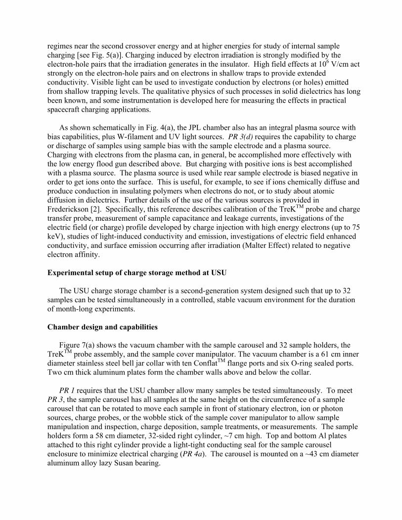
Figure 7(a) shows the vacuum chamber with the sample carousel and 32 sample holders, the TreKTM probe assembly, and the sample cover manipulator. The vacuum chamber is a 61 cm inner diameter stainless steel bell jar collar with ten ConflatTM flange ports and six O-ring sealed ports. Two cm thick aluminum plates form the chamber walls above and below the collar.
PR 1 requires that the USU chamber allow many samples be tested simultaneously. To meet
PR 3, the sample carousel has all samples at the same height on the circumference of a sample carousel that can be rotated to move each sample in front of stationary electron, ion or photon sources, charge probes, or the wobble stick of the sample cover manipulator to allow sample manipulation and inspection, charge deposition, sample treatments, or measurements. The sample holders form a 58 cm diameter, 32-sided right cylinder, ~7 cm high. Top and bottom Al plates attached to this right cylinder provide a light-tight conducting seal for the sample carousel enclosure to minimize electrical charging (PR 4a). The carousel is mounted on a ~43 cm diameter aluminum alloy lazy Susan bearing.
Each sample can be positioned in front of a single field probe using a rotary feedthrough to facilitate the very large number of precise field measurements required in the long-term studies. Rotation is accomplished with astandard vacuum rotary feedthough mounted below the carousel, shown iFigure 7(b). The
rotary shaft flange is attached to the center of the sample carousel base plate; this couples the basplate to the rotary feedthough shaft. The angular position of the sample carousel is set by fitting a pin into one of 32 holes on a rotary motion positioning plate attached to the rotating exterotary feedthrough. The four holes visible in the rotary shaft flange [see Fig. 7(a)] provide accefor coaxial electrical cables and cryogen lines from the feedthroughs below into the sample carousel enclosure. Two 20-pin electrical feedthroughs, mounted on a six-way cross, provide access for the coaxial leads to each sample electrode. A four-lead MHV electrical connector attached to another port of the six-way cross; lead connections are made to a Faraday cupdiagnostics on the sample carousel. A solenoid vacuum valve is connected to the six-way cross; this provides a connection from the turbo pump vacuum system to the charge storage chamber. All electrical connections are made inside the sample carousel enclosure to minimize electrical noise and to prevent extraneous sample charging. The cryogen feedthrough is also attached to the six-way cross. One sample position on the sample carousel has a flat metal sample to serve as both field probe calibrator and as the zero-set sample. Other positions will have a Faraday cup and UV sensitive photodiode to calibrate the flux of the charged particle and photon radiation, respectively (PR 2c and 3f).
(a) (b) Figure 7 (a) Interior view of the USU charge storage chamber
showing the (A) sample carousel, (B) sample holders, (C) charge probe assembly, (D) sample cover manipulator, and (E) electron gun port. (b) Detail of vacuum rotary feedthrough that allows the sample on the carousel to be moved in front of the electron gun, TreKTM probe, etc.
n the
e
rior of the ss
is and other
Sample holder design
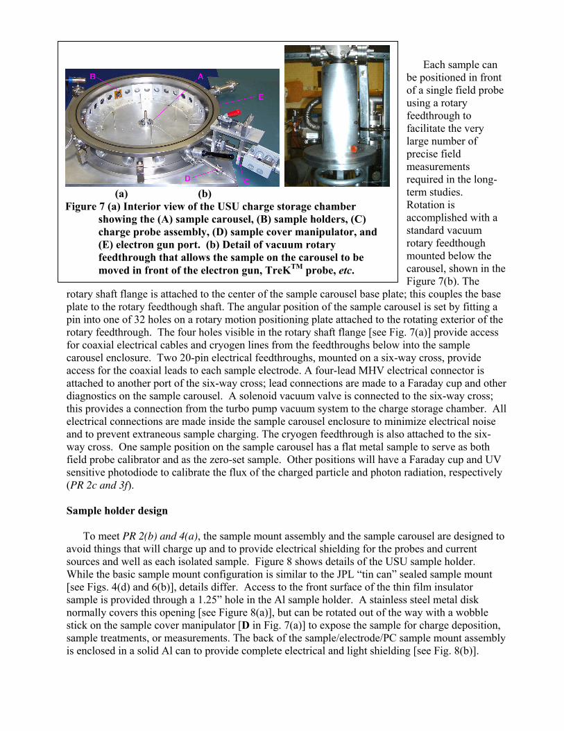
To meet PR 2(b) and 4(a), the sample mount assembly and the sample carousel are designed to avoid things that will charge up and to provide electrical shielding for the probes and current sources and well as each isolated sample. Figure 8 shows details of the USU sample holder. While the basic sample mount configuration is similar to the JPL “tin can” sealed sample mount [see Figs. 4(d) and 6(b)], details differ. Access to the front surface of the thin film insulator sample is provided through a 1.25” hole in the Al sample holder. A stainless steel metal disk normally covers this opening [see Figure 8(a)], but can be rotated out of the way with a wobble stick on the sample cover manipulator [D in Fig. 7(a)] to expose the sample for charge deposition, sample treatments, or measurements. The back of the sample/electrode/PC sample mount assembly is enclosed in a solid Al can to provide complete electrical and light shielding [see Fig. 8(b)].
The sample mounting configuration to the Al sample holder is functionally equivalent to that used in the JPL design [see Fig. 6(c)]. A ~250 µm Kapton tape on the inner surface of the sample holder isolates it from the front surface of the sample. Each insulating sample is mounted with UHV compatible glue on its own ~50 mm diameter polycarbonate sample mount [see Fig. 8(c)]. A thin back electrode made of ~125 µm thick Cu foil, ~3.8 cm in diameter, with no guard electrode, is glued topolycarbonate sample mount. An electrical connection to the back electrode is made via a phosphor bronze spring held in place with a Be-Cu clip and screw on the polycarbonate sample mount using UHV compatible KaptonTM-coated coaxial ground-shielded cable leading out the back. The sample/electrode/PC sample mount assembly is then mounted (using two Nylon screws) to one of the 32 sample holders on the sample carousel. Stainless steel set screws are inserted into the front of the two through-tapped holes to prevent the insulating surface of these nylon screws from being visible to incident electrons. A Be-Cu tension relief clamp visible on the bottom of the sample holder provides strain relief for the coaxial cable.
the
TreKTM Probe Details
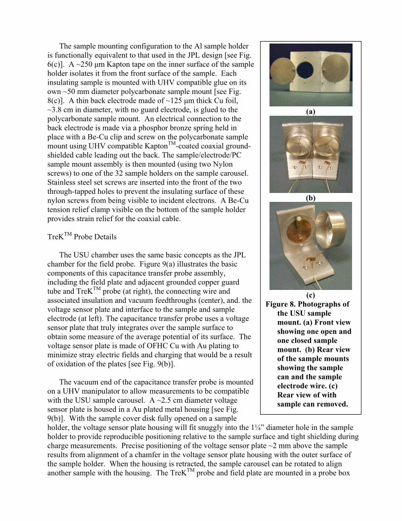
The USU chamber uses the same basic concepts as the JPL chamber for the field probe. Figure 9(a) illustrates the basic components of this capacitance transfer probe assembly, including the field plate and adjacent grounded copper guard tube and TreKTM probe (at right), the connecting wire and associated insulation and vacuum feedthroughs (center), and. the voltage sensor plate and interface to the sample and sample electrode (at left). The capacitance transfer probe uses a voltage sensor plate that truly integrates over the sample surface to obtain some measure of the average potential of its surface. The voltage sensor plate is made of OFHC Cu with Au plating to minimize stray electric fields and charging that would be a result of oxidation of the plates [see Fig. 9(b)].
The vacuum end of the capacitance transfer probe is mounted
on a UHV manipulator to allow measurements to be compatible with the USU sample carousel. A ~2.5 cm diameter voltage sensor plate is housed in a Au plated metal housing [see Fig. 9(b)]. With the sample cover disk fully opened on a sample holder, the voltage sensor plate housing will fit snuggly into the 1¼” diameter hole in the sample holder to provide reproducible positioning relative to the sample surface and tight shielding during charge measurements. Precise positioning of the voltage sensor plate ~2 mm above the sample results from alignment of a chamfer in the voltage sensor plate housing with the outer surface of the sample holder. When the housing is retracted, the sample carousel can be rotated to align another sample with the housing. The TreKTM probe and field plate are mounted in a probe box
(a)
(b)
(c) Figure 8. Photographs of
the USU sample mount. (a) Front view showing one open and one closed sample mount. (b) Rear view of the sample mounts showing the sample can and the sample electrode wire. (c) Rear view of with sample can removed.

[see Fig. 9(2)], that move with the voltage sensor plate maintaining the precise 3 mm gap between the TreKTM probe and field plate. Sample Treatment
A custom designed miniature W-filament low energy flood gun, described in more detail in Thomson [13,14], is a source of monochromatic low energy electrons required to meet PR 3(c). To meet PR 3(e), a medium energy electron flood gun will be installed for uniform, stable charge deposition at energies in the few keV regime near the second crossover energy for the insulators to be studied. The gun will be mounted on an available ConflatTM flange on the vacuum chamber to allow charging of one sample at a time [PR 3(a)]. Beam currents and beam profiles will be monitored with a standard Faraday cup mounted on the sample carousel.
To provide optical access to the samples to treat samples with UV/VIS light and to discharge
samples using light [PR 3(f)], a standard UV-grade sapphire viewport mounted on a Conflat flange is attached to the chamber bell jar collar [see Fig. 7(a)]. Broadband W-filament and Dueterium or Hg discharge sources and IR/VIS/UV quasi-monochromatic LED external light sources can be mounted on the viewport flange as required. An additional quartz viewport is available for visual inspection of the samples. Both viewports are equipped with external covers to block light from entering the chamber, light that might result in sample charging through the photoelectric effect, except when des
grounded electrode
sample
field plate
TreK probe
connecting wire
(a)
(b) (c)
Figure 9. (a) Schematic of charge probe assembly showing the TreKTM probe and grounded copper guard tube (right), capacitance transfer probe–consisting of field plate, connecting wire and voltage sensor plate (center), and sample and grounded sample electrode (left) (b) Photograph of the USU TreKTM probe assembly with translation mechanism. (c) Translation mechanism mounted on the vacuum chamber with the sample electrode and the TreKTM
probe box attached.
ired.
tely one
Sample environment-vacuum system and temperature
In order to measure long charge decay time constants, one must provide continuous high vacuum testing, without exposure to even partial vacuum, with approximameasurement per sample per day for about a month (PR 4b). Gas conduction activated by background radiation is a limitation for our methods. It will slowly discharge samples, or bring charge from one sample to another. The vacuum system

must therefore work steadily at an operating pressure of ~10-7 Torr. Figure 10 gives the details of the vacuum system used at USU. The vacuum chamber uses a 55 liter/sec turbomolecular pump backed by a ~150 liter/s, two-stage, direct-drive, rotary-vane mechanical vacuum pump with a bakeable molecular sieve trap to minimize contamination due to backstreaming. Pressure is measured by a low-pressure nude UHV ion gauge (10-5 to 10-10 Torr), an intermediate pressure Convectron gauge (10-4 to 10+3 Torr), and a high pressure Si strain gauge transducer (100 to 10+6 Torr). Relative humidity is monitored over a 0% to 100% range with a 2% accuracy using a standard gauge.
The experiment environment requires temperature control of the samples over the lifetime of
the experiments, on the order of a month (PR 4c). Typical experiments to compare temperature dependence with theory for polymer insulator resistivity require ~±50 °C about room temperature [2]. Temperature control of the entire sample carousel is provided by two heat reservoirs attached to the carousel base plate. The unit is designed to control the temperature of the samples and entire sample carousel to ~±5 °C using a standard PID temperature controller and platinum resistance thermometers. Thermal isolation of the sample carousel from the rest of the chamber results from the weak thermal link across the lazy Susan bearing. The heat reservoirs can be filled with cooled or heated water from a closed loop system in contact with an external temperature bath, or with liquid nitrogen or other cryogens; they can also be heated with resistance heaters. Alternately, the heat reservoirs can act as thermal reservoirs to dissipate excess heat, via a heat transfer fluid, from four 70 W thermoelectric Peltier cooling units. The Peltier coolers, situated below the heat reservoirs in thermal contact with the carousel base plate, are designed to control the sample to ±100 °C.
Computer interface
To meet PR 4(a) to maintain vacuum and instrument functions for the life of the experiments (on the order of one month), a PC computer has been assembled with extensive hardware and software interface capabilities. Instrumentation control is implemented using LabviewTM to automate the data collection and sample manipulation, to facilitate rapid surface charge measurements thereby minimizing the likelihood of disturbing charge on the samples. Analog inputs on the standard data acquisition card (DAC) are used to monitor various voltage signals including: output from the high voltage supply; temperature controller signals; beam voltage, filament current, and extractor voltage from the electron flood gun power supply and medium energy electron gun controller; and the electrostatic field strength from the TreKTM probe controller. Digital outputs from the DAC card are used to enable the output of the low voltage and high voltage power supplies, to trigger a
L
H
G K
B J
I
A
F
DCE
Figure 11. Assembly of the charge storage chamber vacuum system A—Turbo pump controller B— Nude UHV ion gauge C— Automatic solenoid valve D— Gas handling system valve E— Solenoid valve F— Bakeable molecular sieve trap G— Exhaust oil mist filter H—Vacuum gauge controller I— ~150 litre/s mech. vacuum pump J— High pressure Si strain gauge transducer K— Turbo molecular pump L— Convectron gauge

reading of the TreKTM probe controller, and to provide beam blanking signals to the electron gun controllers. In addition, a GPIB interface card and USB ports are used to control instruments including power supplies, multimeters, and electrometers.
(a) (b)
Figure 11. (a) Surface voltage decay measurement on four samples. The top three curves are for 25 µm (proprietary) silicate glass samples, initially charged to -300 VDC. The bottom sample is for a 0.8 mm thick FR4 circuit board, initially charged to -600 V DC. (b) Surface voltage decay for the two polyimide samples. Low-energy electron charging occurred at 0 days and resulted in the solid data points. Electron beam charging occurred at 23.7 days resulting in the open data points
A serial port-interfaced vacuum gauge controller is used monitor and control all vacuum gauges and vacuum processes for the charge storage chamber, the capacitance resistance apparatus, the gas handling system, and the turbo pumped vacuum system. The vacuum gauge controller reads signals from two UHV nude ion gauges, two low vacuum Convectron gauges, a low vacuum thermocouple gauge, an intermediate pressure capacitance manometer, a high pressure Si strain gauge, and a relative humidity gauge. The vacuum gauge controller also monitors digital input from the turbo pump controller and sentry valve and uses internal relays to open and close the Varian solenoid-controlled valve, the turbo vent valve, and small solenoid valves to the capacitance resistance apparatus and the gas handling system. The correct order of valve operation and pump restart in the event of a power failure or vacuum interrupt is controlled by the vacuum controller. Power to the vacuum controller, computer, valves and turbo pump controller are provided by an uninterruptible power supply in the event of power failure or surges. Results of charge storage method
Figures 11(a) [1] and 11(b) [2] show charge storage decay curves for six different materials. In each case, the resistivity is two to four orders of magnitude larger than that obtained with classical methods. For example, the charge storage value of resistivity for aluminum-backed 51 µm Kapton H samples [11] was >5·10+19 Ω·cm [see Fig. 11(b)], compared to a value of ~(3±1) ·10+16 Ω·cm measured with classical methods (see Fig. 3).

Acknowledgments
This work was supported by the NASA Space Environments and Effects (SEE) Program [8] and a USU Space Dynamics Laboratory Enabling Technologies Program Research Grant.

References
1. A.R. Frederickson, C. E. Benson and J. F. Bockman, “Measurement of Charge Storage and Leakage in Polyimides,” Nuclear Instruments and Methods in Physics Research B, 454-60, 2003.
2. A.R. Frederickson and J. R. Dennison, “Measurement of Conductivity and Charge Storage
in Insulators Related to Spacecraft Charging,” accepted for publication in IEEE Trans. Nuc. Sci., Dec. 2003.
3. J.R. Dennison, C.D. Thomson, J. Kite, V. Zavyalov, Jodie Corbridge, “Materials
Characterization At Utah State University: Facilities And Knowledgebase Of Electronic Properties Of Materials Applicable To Spacecraft Charging,” Proceedings of the 8th Spacecraft Charging Technology Conference, October 20-24, 2003, Huntsville, Alabama.
4. A.Robb Frederickson and Donald H. Brautigam, “Mining CRRES IDM Pulse Data and
CRRES Environmental Data to Improve Spacecraft Charging/Discharging Models and Guidelines,” Final Report: NASA SEE Program Contract No. NAS7-1407, Task Order 10676, 2003; to be published.
5. W. Tillar Shugg, Handbook of Electrical and Electronic Insulating Materials, 2nd Ed; The
Guide to Plastics by the Editors of Modern Plastics Encyclopedia, McGraw Hill, Inc., N.Y., 1970.
6. ASTM D 257-99, “Standard Test Methods for DC Resistance or Conductance of Insulating
Materials” (American Society for Testing and Materials, 100 Barr Harbor drive, West Conshohocken, PA 19428, 1999).
7. IEC 93, International Electrotechnical Commission Publication 93, Methods of Test for
Volume Resistivity and Surface Resistivity of Solid Electrical Insulating Materials, Second Edition, 1980.
8. J.R.Dennison and A.R.Frederickson, “Electronic properties of materials with application
to spacecraft charging”, NASA Space Environments and Effects (SEE) Program Grant NAS8- 02031,.2002-2004.
9. J. M. Bodeau, private communications, 2003. 10. J.R. Dennison, A. R. Frederickson, Prasanna Swaminathan, “Charge Storage, Conductivity
And Charge Profiles Of Insulators As Related To Spacecraft Charging,” Proceedings of the 8th Spacecraft Charging Technology Conference, October 20-24, 2003, Huntsville, Alabama.
11. Kapton polyimide film product information: Physical Properties, Report H-38492-1,
(Dupont, Wilmington, DE, February, 1997); http://www.dupontteijinfilms.com/ , June 20, 2002; The Red Book, RB 1, (Sheldahl Technical Materials, Northfield MN, 1995); http://www.sheldahl.com/Product/TechMaterials.htm , June 20, 2002.

12. Operators Manual, Model 341A, High Voltage Electrostatic Voltmeter, Trek, Inc., 11601 Maple Ridge Road, Medina, New York 14103, USA. Telephone: 1 (800) 367-8735 or 1 (585) 798-3140, http://www.trekinc.com/ .
13. C.D. Thomson, Measurements of the Secondary Electron Emission Properties of
Insulators, Ph.D. dissertation, Utah State University, 2004. 14. C.D. Thomson, V. Zavyalov, J.R. Dennison, Jodie Corbridge, “Electron Emission
Properties Of Insulator Materials Pertinent To The International Space Station,” Proceedings of the 8th Spacecraft Charging Technology Conference, October 20-24, 2003, Huntsville, Alabama.
15. J.R. Dennison, W.Y. Chang, N. Nickles, J. Kite, C.D. Thomson, Jodie Corbridge, and Carl
Ellsworth, “Final Report Part III: Materials Reports,” NASA Space Environments and Effects Program Grant, “Electronic Properties of Materials with Application to Spacecraft Charging,” September 2002; Available in electronic format through NASA SEE as part of the SEE Charge Collector Knowledgebase.