Embed Size (px)
Citation preview

© 2016 IEEE
IEEE Journal of Emerging and Selected Topics in Power Electronics (JESTPE), Vol. 4, No. 2, pp. 638-656, June 2016
Comprehensive Conceptualization, Design, and Experimental Verification of a Weight-OptimizedAll-SiC 2 kV/700 V DAB for an Airborne Wind Turbine
C. Gammeter,F. Krismer,J. W. Kolar
This material is published in order to provide access to research results of the Power Electronic Systems Laboratory / D-ITET / ETH Zurich. Internal or personal use of this material is permitted. However, permission to reprint/republish this material for advertising or promotional purposes or for creating new collective works for resale or redistribution must be obtained from the copyright holder. By choosing to view this document, you agree to all provisions of the copyright laws protecting it.

638 IEEE JOURNAL OF EMERGING AND SELECTED TOPICS IN POWER ELECTRONICS, VOL. 04, NO. 2, JUNE 2016
Comprehensive Conceptualization, Design, andExperimental Verification of a Weight-Optimized
All-SiC 2 kV/700 V DAB for anAirborne Wind Turbine
Christoph Gammeter, Student Member, IEEE, Florian Krismer, Member, IEEE,and Johann W. Kolar, Fellow, IEEE
Abstract— This paper details the design, implementation, andexperimental verification of a minimum weight input seriesoutput parallel structured dual active bridge (DAB) converter foran airborne wind turbine system. The main power components ofthe DAB converter, particularly the bridge circuits, the activelycooled high-frequency transformer and inductor, and the coolingsystem, which largely contribute to the total system weight, aredesigned and realized based on multiobjective considerations,i.e., with respect to weight and efficiency. Furthermore, thedesign includes all necessary considerations to realize a fullyfunctional prototype, i.e., it also considers the auxiliary supply,the control for a stable operation of the system, which alsocomprises an input filter, over the specified operating range, andthe start-up and shut down procedures. These considerationsshow the complex interactions of the various system parts andreveal that a comprehensive conceptualization is necessary toarrive at a reliable minimum weight design. Experimental resultsvalidate the proposed design procedure for a realized lightweightDAB hardware prototype with a rated power of 6.25 kW. Theprototype weighs 1.46 kg, i.e., features a power-to-weight ratioof 4.28 kW/ kg (1.94 kW/ lb), and achieves a maximum full-loadefficiency of 97.5%.
Index Terms— Aerospace electronics, airborne windturbine (AWT), dc–dc power converters, power electronics,renewable energy, wind power generation.
I. INTRODUCTION
INCREASING consumption of electric energy,environmental issues, and limited availability of fossil
fuels have led to a multitude of developments related tothe generation of electricity from renewable energy sources.One innovative system in this context is the airborne windturbine (AWT) detailed in [1], which generates electricity fromhigh-altitude winds. High-altitude winds are known to be morestable and faster than the winds close to the ground level andthus enable a more reliable and effective generation of electricenergy [1], [2]. The considered AWT is a flying wing with
Manuscript received April 29, 2015; revised July 16, 2015; acceptedJuly 18, 2015. Date of publication July 21, 2015; date of currentversion April 29, 2016. Recommended for publication by AssociateEditor P. Mattavelli.
The authors are with the Power Electronic Systems Laboratory, SwissFederal Institute of Technology Zurich, Zurich 8092, Switzerland (e-mail:[email protected]; [email protected]; [email protected]).
Color versions of one or more of the figures in this paper are availableonline at http://ieeexplore.ieee.org.
Digital Object Identifier 10.1109/JESTPE.2015.2459378
Fig. 1. Electrical system of the AWT. Four bidirectional dc–dc converterslink eight voltage source rectifiers to a power transmission tether (≈1 km).The ground station, i.e., a bidirectional dc–ac converter, connects the tetherto the three-phase grid. Four single converter cells form a bidirectionaldc–dc converter with a dc port voltage V2 of up to 8 kV.
air-powered on-board power generators and is tied tothe ground with an approximately 1-km-long tether. Thetether, a combination of fiber and cable, provides boththe required mechanical strength and the electrical linkto the ground station [1]–[4], which is connected to themedium-voltage (MV) grid.
The greatest challenge with respect to the realization ofthe electric system of the considered AWT, with a totalmaximum input power of 100 kW, is to achieve a lightweighttether [1]–[4], lightweight generators [1], [5]–[10], and powerconverters [1], [11]–[27]. From related investigations detailedin [1], the electrical system shown in Fig. 1 emerges, whichuses low-voltage (LV) generators and inverters, operated froma dc bus voltage ranging from 650–750 V, dc–dc convertersthat convert the LV dc bus voltage into a high tether voltageof up to 8 kV, the tether itself, and the ground station.The AWT system considers four identical dc–dc converters forsafety reasons. With the proposed electrical system structure,a failure of any on-board power conversion system componentwill result at most in the loss of two propulsion systems.
2168-6777 © 2015 IEEE. Personal use is permitted, but republication/redistribution requires IEEE permission.See http://www.ieee.org/publications_standards/publications/rights/index.html for more information.
GAMMETER et al.: CONCEPTUALIZATION, DESIGN, AND EXPERIMENTAL VERIFICATION OF A WEIGHT-OPTIMIZED ALL-SiC 2 kV/700 V DAB 639
TABLE I
SPECIFICATIONS FOR THE AWT DC–DC TRANSMISSION SYSTEM
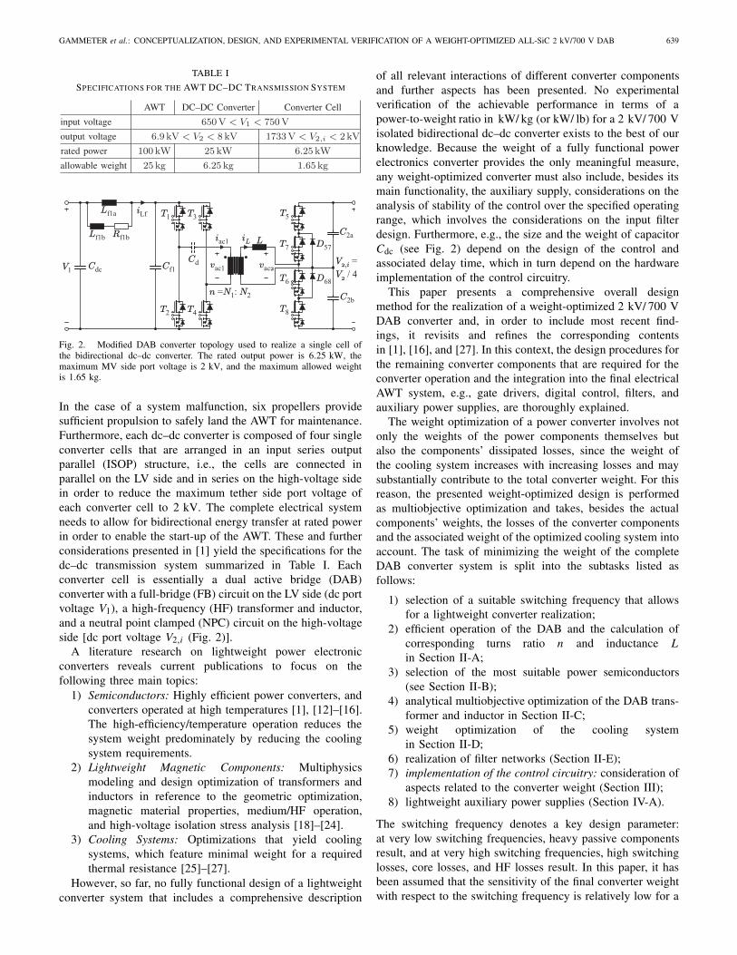
Fig. 2. Modified DAB converter topology used to realize a single cell ofthe bidirectional dc–dc converter. The rated output power is 6.25 kW, themaximum MV side port voltage is 2 kV, and the maximum allowed weightis 1.65 kg.
In the case of a system malfunction, six propellers providesufficient propulsion to safely land the AWT for maintenance.Furthermore, each dc–dc converter is composed of four singleconverter cells that are arranged in an input series outputparallel (ISOP) structure, i.e., the cells are connected inparallel on the LV side and in series on the high-voltage sidein order to reduce the maximum tether side port voltage ofeach converter cell to 2 kV. The complete electrical systemneeds to allow for bidirectional energy transfer at rated powerin order to enable the start-up of the AWT. These and furtherconsiderations presented in [1] yield the specifications for thedc–dc transmission system summarized in Table I. Eachconverter cell is essentially a dual active bridge (DAB)converter with a full-bridge (FB) circuit on the LV side (dc portvoltage V1), a high-frequency (HF) transformer and inductor,and a neutral point clamped (NPC) circuit on the high-voltageside [dc port voltage V2,i (Fig. 2)].
A literature research on lightweight power electronicconverters reveals current publications to focus on thefollowing three main topics:
1) Semiconductors: Highly efficient power converters, andconverters operated at high temperatures [1], [12]–[16].The high-efficiency/temperature operation reduces thesystem weight predominately by reducing the coolingsystem requirements.
2) Lightweight Magnetic Components: Multiphysicsmodeling and design optimization of transformers andinductors in reference to the geometric optimization,magnetic material properties, medium/HF operation,and high-voltage isolation stress analysis [18]–[24].
3) Cooling Systems: Optimizations that yield coolingsystems, which feature minimal weight for a requiredthermal resistance [25]–[27].
However, so far, no fully functional design of a lightweightconverter system that includes a comprehensive description
of all relevant interactions of different converter componentsand further aspects has been presented. No experimentalverification of the achievable performance in terms of apower-to-weight ratio in kW/ kg (or kW/ lb) for a 2 kV/ 700 Visolated bidirectional dc–dc converter exists to the best of ourknowledge. Because the weight of a fully functional powerelectronics converter provides the only meaningful measure,any weight-optimized converter must also include, besides itsmain functionality, the auxiliary supply, considerations on theanalysis of stability of the control over the specified operatingrange, which involves the considerations on the input filterdesign. Furthermore, e.g., the size and the weight of capacitorCdc (see Fig. 2) depend on the design of the control andassociated delay time, which in turn depend on the hardwareimplementation of the control circuitry.
This paper presents a comprehensive overall designmethod for the realization of a weight-optimized 2 kV/ 700 VDAB converter and, in order to include most recent find-ings, it revisits and refines the corresponding contentsin [1], [16], and [27]. In this context, the design procedures forthe remaining converter components that are required for theconverter operation and the integration into the final electricalAWT system, e.g., gate drivers, digital control, filters, andauxiliary power supplies, are thoroughly explained.
The weight optimization of a power converter involves notonly the weights of the power components themselves butalso the components’ dissipated losses, since the weight ofthe cooling system increases with increasing losses and maysubstantially contribute to the total converter weight. For thisreason, the presented weight-optimized design is performedas multiobjective optimization and takes, besides the actualcomponents’ weights, the losses of the converter componentsand the associated weight of the optimized cooling system intoaccount. The task of minimizing the weight of the completeDAB converter system is split into the subtasks listed asfollows:
1) selection of a suitable switching frequency that allowsfor a lightweight converter realization;
2) efficient operation of the DAB and the calculation ofcorresponding turns ratio n and inductance Lin Section II-A;
3) selection of the most suitable power semiconductors(see Section II-B);
4) analytical multiobjective optimization of the DAB trans-former and inductor in Section II-C;
5) weight optimization of the cooling systemin Section II-D;
6) realization of filter networks (Section II-E);7) implementation of the control circuitry: consideration of
aspects related to the converter weight (Section III);8) lightweight auxiliary power supplies (Section IV-A).
The switching frequency denotes a key design parameter:at very low switching frequencies, heavy passive componentsresult, and at very high switching frequencies, high switchinglosses, core losses, and HF losses result. In this paper, it hasbeen assumed that the sensitivity of the final converter weightwith respect to the switching frequency is relatively low for a

640 IEEE JOURNAL OF EMERGING AND SELECTED TOPICS IN POWER ELECTRONICS, VOL. 04, NO. 2, JUNE 2016
switching frequency close to the optimal switching frequency,i.e., a flat optimum. For this reason, the complete AWT sys-tem has initially been optimized for six different switch-ing frequencies ( fs = 50 kHz, 80 kHz, 100 kHz, 125 kHz,160 kHz, and 200 kHz), using simplified models and practice-oriented assumptions; the obtained results suggest a switchingfrequency of approximately 100 kHz. With the determinedswitching frequency, the remaining items 2)–8) of the listcan be processed in the given sequence in order to optimizethe DAB converter with respect to minimum weight. Finally,Section V presents the experimental results demonstratingthe achieved performance of 4.28 kW/ kg (1.94 kW/ lb) of aprototype system, and this paper concludes with an outlookin Section VI.
II. MINIMUM WEIGHT POWER CONVERTER
This section details the design or the selection of powercomponents suitable for a lightweight power converter,i.e., power semiconductors, HF transformer and inductor, andthe components of the filter networks. Prior to this, however,the converter’s turns ratio, n, and HF inductance, L, needto be determined in order to allow for the calculation of alloperating-point-dependent voltage and current waveforms theDAB converter is subject to.
A. Optimal Converter Operation, Optimal n and L
The investigated DAB converter is operated most efficientlyat V1/n ≈ V2,i/2 with the conventional phase shift modula-tion (CPM) scheme [28]. Thus, the turns ratio of the DABtransformer is
n = V1
V2,i/2= 750 V
1 kV= 0.75. (1)
The CPM scheme needs to be slightly modified, since theMV side NPC converter requires a minimum freewheelingtime of 250 ns in order to ensure an equal distribution of theblocking voltages across the switches T5, . . . , T8 [16]. Withthis, the voltage and the current waveforms shown in Fig. 3(a)result, i.e., a maximum duty cycle of the NPC converter ofD2 = (0.5 − 250 ns · fs) = 0.475 results. The correspondingmaximum allowable DAB inductance, L, for a maximum dutycycle of the NPC converter and the specified rated power isdetermined with
L = min(V1V2,i )
4n fsPi,maxηexp
[ϕmax
π
(1 − ϕ2
max
π2
)−
(1
2− D2
)2]
= 107 µH (2)
calculated for Pi,max = 6.25 kW, a conservative value ofthe expected efficiency,1 ηexp = 95%, and the maximumsteady-state phase angle ϕmax = π/4 (in order to maintaina good controllability at low output power, typically
1For a more accurate estimation of the expected efficiency, it needs to bepart of the converter optimization, i.e., ηexp is a result of each particularconverter design. However, a relatively small impact of a minor changeof ηexp, e.g., from 95%–97.5%, on the final losses and total weight is expectedand, therefore, ηexp = 95% is maintained throughout the whole converterdesign procedure. The conservative value of 95% is selected in order to takea slight safety margin for the required cooling system into account.
Fig. 3. (a) Voltage and current waveforms calculated for a singleDAB converter (V1 = 700 V, V2,i = 1.9 kV, Pi = 6.25 kW/ηexp,ηexp = 95%, n = 0.75, L = 107 µH, and fs = 100 kHz); the NPC converteron the MV side requires a freewheeling time of 250 ns. (b) Power transfercharacteristics of the DAB (see [28]), V1/V2,i = 0.375 = constant; maximumpower transfer is achieved for ϕ = ±π/2. Dashed line: rms inductor currentIL (ϕ) at the nominal operation.
TABLE II
TRANSFORMER, CAPACITOR, AND SEMICONDUCTOR CURRENTS
OF A SINGLE DAB CONVERTER MODULE WITH
Pi = 6.25 kW/ηexp AND ηexp = 95% [1]
ϕmax ∈ [π/4, π/3]). With known values of n and L, thecharacteristic converter currents can be calculated using themethods presented in [28]. These currents are summarizedin Table II.
B. Power Semiconductors
SiC power semiconductors are considered to be mostsuitable with respect to low losses and, subsequently, lowweights of the heat sinks required for active cooling. Forthe MV side NPC converter, normally ON SiC JFETs in aTO-247 package with breakdown voltages of 1700 V andlow ON-state resistances of 150 m� at 125 °C are selected.Each SiC JFET is connected in series to a LV p-channel SiMOSFET (FDMS6681Z, RDS,ON = 3.2 m�), and a gate driverespecially dedicated to SiC JFETs operates both devices (hereInfineon’s 1EDI30J12CP EiceDriver is used), to gain normallyOFF properties. The LV side FB converter employs SiC JFETswith breakdown voltages of 1200 V and ON-state resistancesof 100 m� at 125 °C. Again, one LV p-channel Si MOSFET(FDMS6681Z, RDS,ON = 3.2 m�) is connected

GAMMETER et al.: CONCEPTUALIZATION, DESIGN, AND EXPERIMENTAL VERIFICATION OF A WEIGHT-OPTIMIZED ALL-SiC 2 kV/700 V DAB 641
in series to each JFET, and the 1EDI30J12CP EiceDriver isused.2
1) Considered Weight: The weight attributed to the powersemiconductors is equal to the sum of the weights ofthe eight JFETs, p-channel MOSFETs, and gate drivers,and the belonging PCB. This weight does not include thecooling systems’ weights, which are separately consideredin Section II-D.
The total weight of all JFETs and p-channel MOSFETsis msemi = 48.8 g, and the PCB and connector’s weightis 49 g. The total weight of all gate drivers is mdrv = 24 g.This includes eight 1EDI30J12CP EiceDriver devices, theconnected SMD resistors and capacitors, and the corre-sponding part of the PCB with an estimated total surfaceof 500 mm2 (for the two layer PCB with a height of 1.6 mm,an average density of 2.24 g/cm3 is assumed).
2) Conduction and Switching Losses: For the optimizationof the cooling system, presented in Section II-D, the lossesgenerated by the converter’s semiconductors need to be known.The considered loss model accounts for conduction andswitching losses.
The conduction losses are calculated based on the ON-statechannel resistance at an assumed junction temperatureof 125 °C (see [29])
PT1,2,3,4,cond = 4 · RDS,ON,I I 2T1,2,3,4,rms = 4 · RDS,ON,I
I 2ac1,rms
2(3)
PT5,6,7,8,cond = 4 · RDS,ON,II I 2T5,6,7,8,rms = 4 · RDS,ON,II
I 2L ,rms
2(4)
with RDS,ON,I = 100 m� and RDS,ON,II = 150 m�.In the realized converter prototype, each previously used
cascode circuit of a JFET and an n-channel MOSFET(see [16]) is replaced by a series connection of a JFET anda p-channel MOSFET in order to reduce the effective outputcapacitance of each power switch and to achieve a furtherreduction of the switching losses. Dedicated gate driversfeaturing direct drive technology (1EDI30J12CP manufacturedby Infineon) ensure normally OFF properties of the powerswitches. The corresponding switching losses have been mea-sured according to [16] (double pulse measurement) on thefinal converter PCB in order to account for the implications ofparasitic components, e.g., the inductance of the commutationloop. The JFETs are thermally connected to a heat plateto enable switching loss measurements at different junctiontemperatures (Tj = 25 °C and 125 °C are considered).Different switching operations result for the half-bridge (HB)and the NPC converters, due to structural differences of thesecircuits. In this context, the reader is kindly referred to [1],
2No competitive SiC MOSFETs have been available at the time whenthe design of the investigated converter has started. Meanwhile, competitive1200 V MOSFETs are available. Thus, the SiC JFETs of the LV side FBcould be replaced by SiC MOSFETs (e.g., C2M0025120D manufactured byCREE), which would lower the losses at full load by approximately 20 Wand increase the full-load efficiency by 0.3%. Thus, some further weightreduction is feasible with SiC MOSFETs, since the series-connectedLV p-channel MOSFETs are not required. The lower losses, furthermore,would allow a slight reduction of the weight of the heat sink.
Fig. 4. Measured SiC JFET switching energies with the (1EDI30J12CP) andexternal gate resistances {ROFF , RON } = {1 �, 2.6 �} being used. (a) InfineonIJW120R070T1 1.2 kV/70 m� in an HB configuration. (b) Infineon sample1.7 kV/100 m� in an NPC configuration. (c) and (d) Circuit diagrams usedto measure the switching energies in (a) and (b), respectively.
which thoroughly discusses the respective details. In summary,the switching losses of a HB converter, shown in Fig. 4(a),thus only depend on the instantaneous port voltage, V1, andoutput current, iHB. The switching losses of the NPC converter[Fig. 4(b)] additionally depend on the previous states of theswitches T5–T8: for the NPC converter, different switchinglosses result if vNPC switches from ±V2,i to zero [edge withlabel I in Fig. 4(d)] or if vNPC switches from zero to ±V2,i
(Edge II).Fig. 4(a) shows the switching losses measured for the
FB converter at V1 = 650 V and 750 V and Tj = 25 °Cand 125 °C. For positive currents iHB, the condition forZVS is, theoretically, fulfilled and for negative currentsiHB hard switching occurs. According to these results,low switching losses of less than 10 µJ can be achievedfor 1 A < iHB < 8 A.
Fig. 4(b) shows the results obtained for the NPC converter.Similar switching losses are measured for the HB and theNPC converter if the switching operation labeled I in Fig. 4(d)is present. For 2 A < iNPC < 10 A, increased switching lossesresult for Edge II, due to residual turn-ON losses [1].
In Fig. 4(a) and (b), there is a rapid increase in the switchingenergies when the current is approaching zero. For currents0 < iHB < 1 A and 0 < iNPC < 2 A, the semiconductor’seffective output capacitances are incompletely charged ordischarged during the dead-time intervals, i.e., residual

642 IEEE JOURNAL OF EMERGING AND SELECTED TOPICS IN POWER ELECTRONICS, VOL. 04, NO. 2, JUNE 2016
Fig. 5. (a) Considered configuration of the actively cooled HF transformerand inductor (from [1]). (b) Cross section cut through the realized transformerwindings showing the HF litz wires being embedded in the epoxy resin, whichis used for the isolation; the turns ratio is n = NLV/NMV = 21/28, both theHF litz are 200 × 71 µm. The magnified image in the bottom-right cornerenables a detailed view on the embedded HF litz wire.
drain-to-source voltages remain for the switches that are turnedON after the dead-time intervals elapsed and, as a consequence,hard switching operations with turn ON losses result [30].
The switching losses generated by the switches T1 . . . T4and T5 . . . T8 are calculated with
PT1,2,3,4,sw = 2 fs[Esw(V1, iHB1,Tj ) + Esw(V1, iHB2, Tj )] (5)
PT5,6,7,8,sw = 2 fs[Esw,I (V2,i , iNPC1, Tj )
+ Esw,II(V2,i , iNPC2, Tj )] (6)
respectively; iHB1, iHB2, iNPC1, and iNPC2 denote theinstantaneous switch currents at switching, i.e., iHB1 denotesthe current switched by T1 and T2, iHB2 is the currentswitched by T3 and T4, iNPC1 is the current switched byT5 and T6, and iNPC2 is the current switched by T7 and T8[see Figs. 2 and 4(c) and (d)]. The switching energies are,in the case of negative slopes of the voltages vHB and vNPC,evaluated for currents iHB and iNPC flowing in the directionsdefined in Fig. 4(c) and (d), respectively. The switchingenergies for positive and negative voltage slopes are equal,since in the steady-state operation, only the signs of thebridges’ output voltages and currents change during the secondhalf of the switching period.
C. Optimization of the DAB Transformer and Inductor
The optimization of the DAB transformer and inductor isbased on the configuration shown in Fig. 5(a), where boththe transformer and the inductor employ ferrite E-cores; theselected configuration realizes active cooling by means of thedepicted copper plates and heat pipes, which conduct copperand core losses to a heat sink. The theoretical optimizationis conducted in [1], and the obtained results are used forrealization; Table III lists the design parameters of the finallyimplemented DAB transformer and inductor. Compared withthe previously obtained optimization results presented in [1],HF litz wires with increased numbers of strands are usedin order to lower the maximum hot-spot temperatures of theLV and the MV side windings. The hot spots are located in
TABLE III
PARAMETERS OF THE DAB TRANSFORMER AND INDUCTOR
the windings’ end turns, where the selected active coolingsetup is least effective. Furthermore, the formerly suggestedinsulation material, Teflon, has been replaced by epoxy resinin order to eliminate the creepage path between the adjacenttransformer windings and between the windings and the core.The MV side winding is surrounded with 2-mm-thick epoxyresin and is considered to withstand dc voltages of morethan 10 kV [31]–[34]. Fig. 5(b) shows a cross-sectionalview through the LV and the MV side transformer windings,embedded in epoxy resin, and reveals that the enlarged HFlitz wires could still be situated into the available space.The weight of the realized DAB transformer and inductor,including the copper plates, and the heat pipes is 522 g.
D. Minimum Weight Cooling System
The DAB converter requires a cooling system with threeseparate heat sinks to dissipate the heat generated by the JFETsof the NPC and the FB converters and to actively cool theHF transformer and inductor. Due to the ISOP structure of thedc–dc converter system (see Fig. 1), voltages up to 4.75 kVare present between the LV and the MV sides of the firstand the fourth DAB converters. Therefore, the galvanic iso-lation between the MV side heat sink and all LV sidecomponents, including the heat sink used to cool theHF transformer and inductor, of which the core is referredto the potential of the minus port of the LV side, needs tobe designed accordingly. Furthermore, the heat sink used forthe switches of the FB converter is thermally isolated fromthe heat sink used to cool the magnetic components, becausethese heat sinks are operated on different temperatures.3
The design of the cooling system is based on the previouslycalculated maximum losses given in [16],4 which are
Ploss,FB = 57 W, Ploss,NPC = 50 W, Ploss,mag = 80 W.
Fig. 6 shows the equivalent thermal networks forall three cooling systems. The thermal networksshown in Fig. 6(a) and (b) consider one heat sourceper JFET, the corresponding junction-to-case thermalresistances, Rth, j-c, the thermal resistances of the isolatingthermal interfaces, Rth,c-hs, and the thermal resistances
3In the case of a common heat sink for the LV side FB converter and themagnetic components, the LV side semiconductors would heat up the magneticcomponents additionally.
4The revision of the switching loss measurements, using the direct drivetechnology, presented in Section II-B has been carried out with the finalconverter setup, which already required the fully functional cooling system.For this reason, the achieved reduction of the switching losses was unknownat the time the cooling system was designed.

GAMMETER et al.: CONCEPTUALIZATION, DESIGN, AND EXPERIMENTAL VERIFICATION OF A WEIGHT-OPTIMIZED ALL-SiC 2 kV/700 V DAB 643
Fig. 6. Thermal networks of the three cooling systems. (a) LV sidesemiconductors. (b) MV side semiconductors. (c) Transformer and inductor.
of the heat sinks themselves. For reliability, the junctiontemperatures are limited to 120 °C. With this, the thermalresistances shown in Fig. 6, and the losses listed in [16], theworst case base plate temperatures of the heat sinks requiredfor the FB and the NPC converters are
ϑhs,max,FB = 120 °C − 14.25 W × 0.94 K/W = 106 °C (7)
ϑhs,max,NPC = 120 °C − 12.5 W × 0.94 K/W = 108 °C (8)
respectively. With a maximum allowed operating ambienttemperature of ϑamb,max = 40 °C, the thermal resistancerequired for the two heat sinks is calculated according to
Rth,S-a,max,FB = ϑhs,max,FB − ϑamb,max
4 × 14.25 W= 1.17 K/W (9)
Rth,S-a,max,NPC = ϑhs,max,NPC − ϑamb,max
4 × 12.5 W= 1.37 K/W. (10)
A similar calculation is conducted for the heat sink used tocool the HF transformer and inductor, which leads to thecorresponding base plate temperature and the required thermalresistance of the heat sink
ϑhs,max,mag = 77 °C (11)
Rth,S-a,max,tr+ind = ϑhs,max,mag − ϑamb,max
80 W= 0.46 K/W. (12)
In the quest for achieving a minimum weightDAB converter, different heat sink configurations havebeen investigated, and the configuration shown in Fig. 7,which employs four heat sink halves, has been identified to bemost suitable with respect to minimum weight. Two heat sinkhalves are used to cool the HF transformer and inductor (due tothe comparably low value of Rth,S-a,max,tr+ind, i.e., a relativelyhigh cooling capability is required) and the remaining twohalves cool the HB and the NPC converters, respectively.The heat sink used to cool the magnetic componentsrequires a base plate size of Ahs,tr+in = 40 mm × 80 mmto accommodate all heat pipes and ferrite cores. The samebase plate size is used for the remaining two heat sink halvesin order to allow for a simplified construction of theDAB converter and to allow for sufficiently large
Fig. 7. CAD model of the final cooling system configuration. Heat pipesfrom the transformer and inductor connect to the heat sinks on both sides.Thermal and electrical insulation separates the heat sinks for the LV and theMV side semiconductors from the heat sinks cooling the transformer andinductor.
Fig. 8. Minimum cooling system weights, calculated with the optimizationalgorithm detailed in [27], for different base plates to ambient thermalresistances of the different cooling system halves, i.e., mcs = mheat sink halve+(mfan + mduct + miso)/2. Only the 40 mm × 40 mm fans in Table IV areconsidered.
distances between adjacent JFETs due to voltage isolationrequirements.
Fig. 8 shows the minimum cooling system weights,calculated with the optimization algorithm detailed in [27],for different base plates to ambient thermal resistances of thedifferent cooling system halves, i.e., mcs = mheat sink halve +(mfan + mduct + miso)/2; this optimization considers the fanslisted in Table IV. Because the airflows through the heat sinksare coupled, only symmetric heat sink geometries areconsidered, i.e., the heat sinks cooled by one fan feature thesame pressure drop characteristics. The properties of the result-ing minimum weight cooling systems are listed in Table V.The total weight of the cooling system is
mcs,total = mcs,FB + mcs,tr+ind + mcs,NPC
= (75 + 2 × 75 + 75) g = 300 g. (13)

644 IEEE JOURNAL OF EMERGING AND SELECTED TOPICS IN POWER ELECTRONICS, VOL. 04, NO. 2, JUNE 2016
TABLE IV
40 mm × 40 mm AXIAL FANS CONSIDERED IN THE OPTIMIZATION
TABLE V
COOLING SYSTEM PROPERTIES THAT FEATURE SYMMETRIC
HEAT SINKS FOR ALL THREE COOLING SYSTEMS
E. Design of the Filter Networks
The dc–dc converter is part of a generator/drive system,i.e., power electronic converters are connected to both sides.The DAB converter, therefore, is not required to fulfill specificconducted electromagnetic compatibility standards. Still, filternetworks are needed in order to allow for proper converteroperation and to enable the DAB converter cells to beembedded in the ISOP structure, as shown in Fig. 1.5 Fig. 2shows the employed filter networks and the following listmotivates the need for the different filter components.
1) The capacitors Cf1, C2a, and C2b are part of the convertertopology, provide low inductive commutation loops, andstabilize the supply voltages of the bridges.
2) The network formed with Lf1a, Lf1b, and Rf1b enablesthe straightforward paralleling of different DAB con-verter cells on the LV sides (Lf1b and Rf1b introducedamping at the resonance frequency). For this reason,the LV side port currents of each converter cell, iLf, asshown in Fig. 2, are separately measured and controlled(see Section III).
3) The capacitor Cdc is used for energy storage. In theISOP configuration, shown in Fig. 1, a single capacitoris used for four DAB converter cells together. Thecapacitance of this single dc capacitor then is equal tofour times the dc capacitance of a single cell. In the
5On the MV side, four 25 kW DAB converter systems, each composedof four single DAB converter cells, are operated in parallel. Therefore,each 25 kW DAB converter system requires a decoupling inductance witha damping network (see the LV side filter network, as shown in Fig. 2) atthe corresponding MV side dc port. For each of these networks, a weightof 70 g is estimated, which is less than the additionally allowed weightof 400 g (see Section V-A).
TABLE VI
LV FILTER COMPONENTS OF THE DAB
case of stand-alone testing of a single cell, e.g., forthe purpose of verifying the operability and the achievedefficiency of a single cell (which is the case inthis paper), Cdc is populated on the PCB of a singleDAB converter cell.
The emphasis of the filter design is to achieve reliableconverter operation, and no analytical weight optimization iscarried out, because of the relatively little contributions ofthe weights of both filters to the total weight of a singleDAB converter cell, i.e., total weights of 93 g and 59 g andrelative weight contributions of 6% and 4% result for theMV and the LV side filters, respectively. For this reason andfor better readability of the work at hand, the conducted filterdesign is presented in the Appendix. Table VI lists the weightsof the employed LV filter component.
III. CONTROL: CONCEPT AND IMPLEMENTATION
At this point, all main power components have beendesigned or selected. A fully operational DAB converter,however, requires additional circuitries for digital control andauxiliary power supplies, which also add to the total weight.Section III-A details the concept employed for the digital con-trol of four DAB converter cells operated in the ISOP structure.Due to the required galvanic isolation, additional circuitcomponents, i.e., optical transmitters, receivers, and fibers, areneeded to establish digital signaling paths between the LV andthe MV sides. Section III-B details the implemented circuit,which requires solely six such signal paths in order to achievelow weight. For better readability of this paper, the design ofthe digital controllers is given in Appendix C.
A. Concept
The ground station controls the voltage applied to the tetherat the ground V ′
2 (see Fig. 1), which defines the voltage at the

GAMMETER et al.: CONCEPTUALIZATION, DESIGN, AND EXPERIMENTAL VERIFICATION OF A WEIGHT-OPTIMIZED ALL-SiC 2 kV/700 V DAB 645
Fig. 9. Master and slave control block diagram of the dc–dc converter witha feedforward of the instantaneous power requirements of the motor invertersPVSI1 and PVSI2.
MV side dc port of the DAB converter system according tothe discussion presented in Appendix A. The DAB can adjustthe tether current, since the ground station adapts to the actualtether current. Thus, at the MV dc port, the DAB convertersystem is free to control the actual operating power by meansof current control. This property, in combination with thebidirectional power capability, renders the DAB convertersystem to be the ideal component regarding the stabilizationof the LV side dc voltage, V1.
Fig. 9 shows the block diagram for the control of one DABconverter system (out of four), which consists of four seriesconnected DAB converter cells and features a total powerof 25 kW. The following list summarizes the functionalitiesof the different blocks.
1) The power management unit determines the set valuesfor the current controllers of all DAB converter cells inorder to control the LV side dc bus voltage, V1. Thecalculation of the reference current, ILf,ref, in addition,includes the dc port currents of both motor inverters inorder to reduce the required energy buffering capabilityof Cdc + Cf1 (see Appendix B).
2) A master and slave control strategy is chosen to balancethe output voltages of all four DAB converter cells: themaster module controls the input voltage V1, and theslave modules ensure an equal distribution of the outputvoltage V2,i = V2,ref = (1/4)V2. The master moduleprovides the reference value V2,ref to the slave modulesas reference, such that each slave module can adjust itsown transferred power, in order to balance the seriesconnected dc links.
3) The current control loop of each converter cell is realizedon the LV side and according to [35].
B. Implementation
Fig. 10 shows the block diagram of the implementeddigital control hardware. Each converter cell incorporates
Fig. 10. Schematic of the control hardware implementated on eachDAB converter cell.
a microcontroller (TMS320F28335), which handles thecommunication between the connected converter cells and theLV side FPGA, monitors currents and voltages, implementsthe digital control, and calculates the switching times t1, t2,and t3 for minimum transformer rms current accordingto [28]. The FPGA on the LV side (LFXP2-5E-5TN144C)runs a state machine that generates the gate signals forthe LV side FB converter and determines the current stateof the MV side NPC converter, which is 0, 1, 2, or 3(for vac2 = −V2,i , 0, V2,i , or to turn all switches OFF
due to a fault on the LV side, respectively). The stateof the NPC converter is transferred to a second FPGAlocated at the MV side (LCMXO2-640HC-4TG100I) bymeans of two optical fibers (2 bits). This second FPGAgenerates the gate signals for the HV side NPC converter.The control of both the HB and the NPC convertersconsiders the dead-time intervals with durationsof 120 ns.
The proposed implementation requires two further opticalcommunication lines between the LV and MV sides, totransmit the value of the actual port voltage, V2,i , using anRS232 protocol with a baud rate of 2.5 MBd and to signalize afault because of an instantaneous overcurrent.6 Finally, a daisychain connection of all four series connected DAB convertercells is achieved with another two optical communicationlines. These are needed for an initial synchronization of allfour NPC converters and to quickly signalize a fault conditionbetween the different converter cells.
The total weight of the digital control circuitry (includ-ing PCB, optical transmitters, receivers, and fibers) is 133 g(for one DAB converter cell), the total weight the opticaltransmitters, receivers, and fibers is 24.6 g.
IV. AUXILIARY POWER SUPPLIES AND START-UP
Two auxiliary power supplies, situated at the LV andthe MV sides, respectively, provide power to the belongingcontrol, measurement, and gate driver circuits. Section IV-Adetails the design and the implementation of these auxiliarypower supplies, which are based on a resonant L LC convertertopology, achieve low switching losses (ZVS), high switching
6Two protection circuits compare the absolute values of the transformercurrents on the LV and the MV sides, |iac,1| and |iL ,1|, to maximum setvalues. The respective FPGA signals a fault in the case of an instantaneousovercurrent situation, which turns OFF the DAB converter system within lessthan one microsecond.
646 IEEE JOURNAL OF EMERGING AND SELECTED TOPICS IN POWER ELECTRONICS, VOL. 04, NO. 2, JUNE 2016
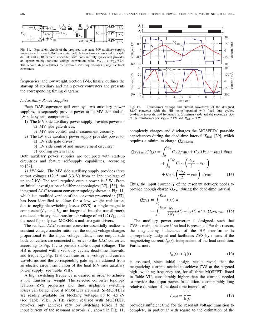
Fig. 11. Equivalent circuit of the proposed two-stage MV auxiliary supply,implemented for each DAB converter cell. A transformer connected to a splitdc link and a HB, which is operated with constant duty cycles and providesan approximately constant voltage conversion ratio, Vaux ≈ V2,i/57.4.The second stage regulates the required auxiliary voltages using LV buckconverters.
frequencies, and low weight. Section IV-B, finally, outlines thestart-up of auxiliary and main power converters and presentsthe corresponding timing diagram.
A. Auxiliary Power Supplies
Each DAB converter cell employs two auxiliary powersupplies, to separately provide power to all MV side and allLV side system components.
1) The MV side auxiliary power supply provides power to:a) MV side gate drives;b) MV side control and measurement circuitry.
2) The LV side auxiliary power supply provides power to:a) LV side gate drives;b) LV side control and measurement circuitry;c) cooling system fans.
Both auxiliary power supplies are equipped with start-upcircuitries and feature self-supply capabilities, accordingto [37].
1) MV Side: The MV side auxiliary supply provides threeoutput voltages (12, 5, and 3.3 V) from an input voltage ofup to 2 kV. The total required output power is 3 W. Froman initial investigation of different topologies [37], [38], theintegrated L LC resonant converter topology shown in Fig. 11,which is a modified version of the converter presented in [37],has been identified to allow for a low weight realization,due to negligible switching losses (ZVS), a single magneticcomponent (Lσ and Lμ are integrated into the transformer),a reduced primary side transformer voltage of ±(1/2)V2,i , andthe need for only two MOSFETs and two gate drivers.
The realized L LC resonant converter essentially realizes aconstant voltage transfer ratio, i.e., the output voltage changesproportional to the input voltage. Thus, three output sidebuck converters are connected in series to the L LC converter,according to Fig. 11, to provide stable output voltages. TheHB is operated with fixed duty cycles, dead-time intervals,and frequency. Fig. 12 shows transformer voltage and currentwaveforms and the corresponding gate signals attained froman electric circuit simulation of the final MV side auxiliarypower supply (see Table VIII).
A high switching frequency is desired in order to achievea low transformer weight. The selected converter topologyfeatures ZVS properties and, thus, negligible switchinglosses can be achieved if MOSFETs are used [Si-MOSFETsare readily available for blocking voltages up to 4.5 kV(see Table VII)]. A HB circuit realized with MOSFETs,however, only achieves very low switching losses if theinput current of the resonant network, i1, shown in Fig. 11,
Fig. 12. Transformer voltage and current waveforms of the designedL LC converter with the HB being operated with fixed duty cycles,dead-time intervals, and frequency at (a) primary side and (b) secondary sideof the transformer for V2,i = 2 kV and Paux = 3 W.
completely charges and discharges the MOSFETs’ parasiticcapacitances during the dead-time interval Tdead [39], whichrequires a minimum charge QZVS,min
QZVS,min(V2,i) =∫ V2,i
0Coss(vHB) + Coss(V2,i − vHB) dvHB
+∫ V2,i
0CTr,1
(V2,i
2− vHB
)
+ CPCB
(V2,i
2− vHB
)dvHB. (14)
Thus, the input current i1 of the resonant network needs toprovide enough charge QZVS during the dead-time interval
QZVS =∫ Tdead
0i1(t) dt
=∫ Tdead
0
N2
k N1i2(t) + iμ(t) dt ≥ QZVS,min. (15)
The auxiliary power converter is designed, such thatZVS is maintained even if no load is presented. For this reason,the magnetizing inductance of the HF transformer isappropriately designed and facilitates ZVS by means of themagnetizing current, iμ(t), independent of the load condition.Furthermore
iμ(t) ≈ i1(t) (16)
is assumed, since initial design results reveal that themagnetizing currents needed to achieve ZVS at the targetedhigh switching frequency are, for all three MOSFETs listedin Table VII, considerably higher than the currents neededto provide the output power. In addition, a comparably longrelative duration of the dead-time interval of
Tdead = 1
6
1
fs(17)
provides sufficient time for the resonant voltage transition tocomplete, in particular with regard to the estimation of the

GAMMETER et al.: CONCEPTUALIZATION, DESIGN, AND EXPERIMENTAL VERIFICATION OF A WEIGHT-OPTIMIZED ALL-SiC 2 kV/700 V DAB 647
TABLE VII
CHARACTERISTIC VALUES DETERMINED FOR THREE DIFFERENT
Si-MOSFETs WITH MAXIMUM DRAIN SOURCE
VOLTAGES OF 4.5 kV
Fig. 13. Voltage waveform at rated input voltage of V2,i = 2 kV andPaux = 3 W. The smooth transitions of the auxiliary transformer voltagewaveform show that the ZVS conditions are fulfilled.
maximum feasible switching frequency, which is estimated inthe following.
Due to the long relative dead time (17), the waveform of thetransformer magnetizing current, iμ(t), is approximated witha sinusoidal waveform (see Fig. 12)
iμ(t) ≈ Iμ,peak sin (2π fst). (18)
With this and (15), the charge QZVS can be calculated
QZVS =∫ 1/(12 fs)
−1/(12 fs)Iμ,peak cos (2π fst) dt = Iμ,peak
2π fs. (19)
Subsequently, under the assumption that QZVS = QZVS,minand with (16)–(18), the conduction losses of the MOSFETs
PT,loss = Rds,ON I 2T,rms = Rds,ON I 2
μ,peak4π − 3
√3
24π(20)
can be calculated, which are limited to
PT ,loss, max = Tj − Tamb
Rth, j-c + Rth,c-a≈ 80 °C
60 K/W≈ 1.3 W (21)
per MOSFET, since passive cooling without additional heatsink is considered [40]. The maximum switching frequencyis obtained from (19) and (20), by eliminating Iμ,peak, forQZVS = QZVS,min
fs ≤√
6PT ,loss,max
π(4π − 3√
3)
1√Rds,ON QZVS,min
. (22)
Table VII summarizes the characteristic values for threeSi-MOSFETs with blocking voltages of 4.5 kV and forCTr,1 = 2 pF and CPCB = 3 pF. Based on this result, the
Fig. 14. (a) MV side auxiliary transformer with four E 13/7/4 N87 corepairs next to a one cent (Euro) coin. (b) 3-D printed bobbin, with 180 turnsof 0.1-mm-diameter and 7 turns of 0.45-mm-diameter enameled copper wire.(c) Schematic of the chosen winding topology, which features a low primarywinding capacitance CTr,1 [41].
switch IXTA02N450HV is selected. However, a reduced finalswitching frequency of fs = 200 kHz, well below the calcu-lated theoretical maximum frequency of fs,max = 345 kHz isselected, since (22) is an approximation and neglects turn OFF
losses and conduction losses due to the load current.According to (19) and (20), the peak value of the
magnetizing current is bounded to
2π fs QZVS,min < Iμ,peak <
√24π
4π − 3√
3
PT ,loss,max
Rds,ON
55 mA < Iμ,peak < 94 mA (23)
which requires a transformer primary inductance of
L1 = Lσ + Lμ = V2,i/2
Iμ,peak
1
2π fs∈ [8.45 mH, 14.5 mH]. (24)
In order to adjust the primary inductance independent ofthe number of primary turns and yield a great number ofdegrees of freedom, stacked E-core transformer designs withan air gap in the magnetic path are considered. The windingtopology is chosen, such that a small parasitic primary windingcapacitance results [41]. Fig. 13 shows the implementedMV auxiliary transformer and a schematic of the windingtopology.
For a given core cross-sectional area Ac, the number ofprimary turns must be
N1 ≥ V2,i/2
4 fs Ac Bmax(25)
with the maximum flux density Bmax = 150 mT for theconsidered ferrite cores. In order to calculate the numberof secondary turns, the leakage inductance Lσ needs to beestimated first to determine the transformer coupling
k =√
Lμ
Lμ + Lσ. (26)
The number of secondary turns is chosen, such that thetransformer output voltage does not exceed the maximumtolerated auxiliary dc-link voltage Vaux,max = 36 V providedto the auxiliary buck converters under no-load conditions(see Fig. 11)
N2 = V2,i/2
k N1· Vaux,max. (27)
648 IEEE JOURNAL OF EMERGING AND SELECTED TOPICS IN POWER ELECTRONICS, VOL. 04, NO. 2, JUNE 2016
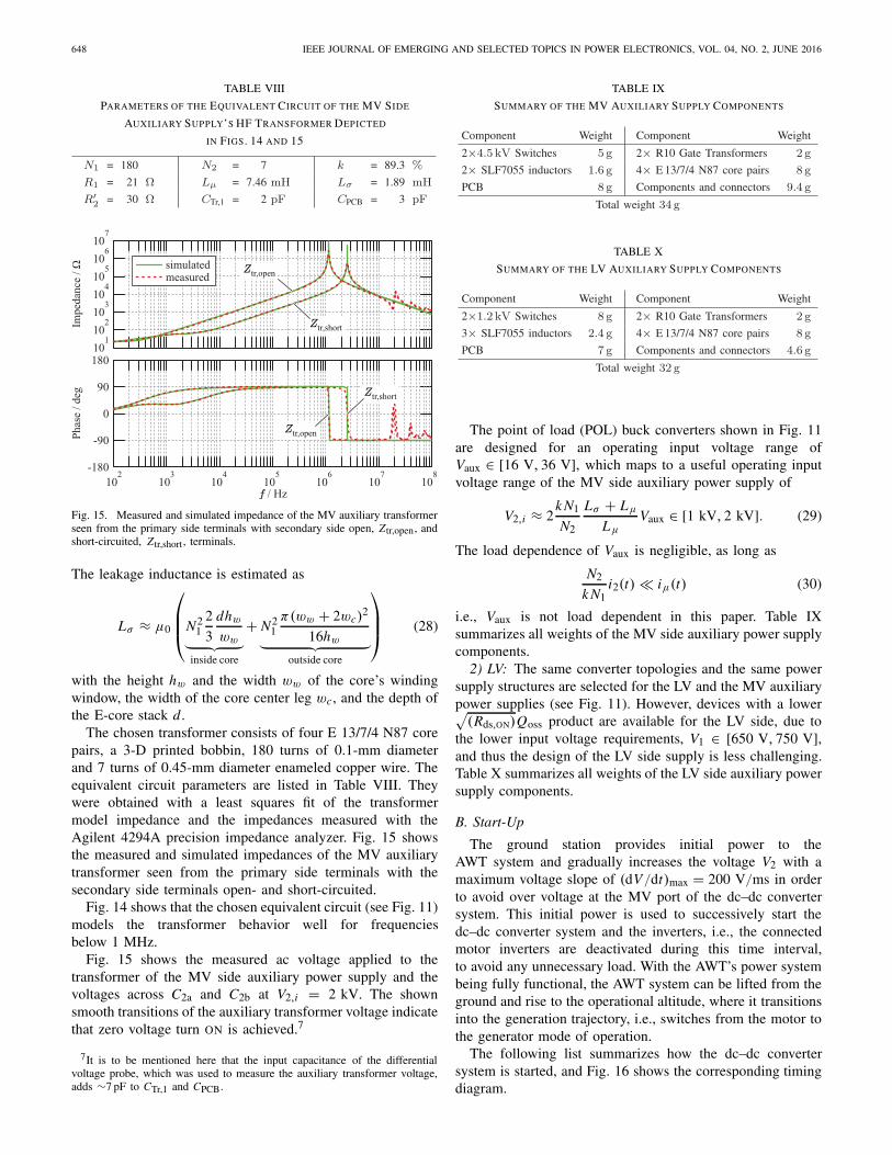
TABLE VIII
PARAMETERS OF THE EQUIVALENT CIRCUIT OF THE MV SIDE
AUXILIARY SUPPLY’S HF TRANSFORMER DEPICTED
IN FIGS. 14 AND 15
Fig. 15. Measured and simulated impedance of the MV auxiliary transformerseen from the primary side terminals with secondary side open, Ztr,open, andshort-circuited, Ztr,short, terminals.
The leakage inductance is estimated as
Lσ ≈ μ0
⎛⎜⎜⎝N2
12
3
dhw
ww︸ ︷︷ ︸inside core
+ N21
π(ww + 2wc)2
16hw︸ ︷︷ ︸outside core
⎞⎟⎟⎠ (28)
with the height hw and the width ww of the core’s windingwindow, the width of the core center leg wc, and the depth ofthe E-core stack d .
The chosen transformer consists of four E 13/7/4 N87 corepairs, a 3-D printed bobbin, 180 turns of 0.1-mm diameterand 7 turns of 0.45-mm diameter enameled copper wire. Theequivalent circuit parameters are listed in Table VIII. Theywere obtained with a least squares fit of the transformermodel impedance and the impedances measured with theAgilent 4294A precision impedance analyzer. Fig. 15 showsthe measured and simulated impedances of the MV auxiliarytransformer seen from the primary side terminals with thesecondary side terminals open- and short-circuited.
Fig. 14 shows that the chosen equivalent circuit (see Fig. 11)models the transformer behavior well for frequenciesbelow 1 MHz.
Fig. 15 shows the measured ac voltage applied to thetransformer of the MV side auxiliary power supply and thevoltages across C2a and C2b at V2,i = 2 kV. The shownsmooth transitions of the auxiliary transformer voltage indicatethat zero voltage turn ON is achieved.7
7It is to be mentioned here that the input capacitance of the differentialvoltage probe, which was used to measure the auxiliary transformer voltage,adds ∼7 pF to CTr,1 and CPCB.
TABLE IX
SUMMARY OF THE MV AUXILIARY SUPPLY COMPONENTS
TABLE X
SUMMARY OF THE LV AUXILIARY SUPPLY COMPONENTS
The point of load (POL) buck converters shown in Fig. 11are designed for an operating input voltage range ofVaux ∈ [16 V, 36 V], which maps to a useful operating inputvoltage range of the MV side auxiliary power supply of
V2,i ≈ 2k N1
N2
Lσ + Lμ
LμVaux ∈ [1 kV, 2 kV]. (29)
The load dependence of Vaux is negligible, as long as
N2
k N1i2(t) iμ(t) (30)
i.e., Vaux is not load dependent in this paper. Table IXsummarizes all weights of the MV side auxiliary power supplycomponents.
2) LV: The same converter topologies and the same powersupply structures are selected for the LV and the MV auxiliarypower supplies (see Fig. 11). However, devices with a lower√
(Rds,ON)Qoss product are available for the LV side, due tothe lower input voltage requirements, V1 ∈ [650 V, 750 V],and thus the design of the LV side supply is less challenging.Table X summarizes all weights of the LV side auxiliary powersupply components.
B. Start-Up
The ground station provides initial power to theAWT system and gradually increases the voltage V2 with amaximum voltage slope of (dV/dt)max = 200 V/ms in orderto avoid over voltage at the MV port of the dc–dc convertersystem. This initial power is used to successively start thedc–dc converter system and the inverters, i.e., the connectedmotor inverters are deactivated during this time interval,to avoid any unnecessary load. With the AWT’s power systembeing fully functional, the AWT system can be lifted from theground and rise to the operational altitude, where it transitionsinto the generation trajectory, i.e., switches from the motor tothe generator mode of operation.
The following list summarizes how the dc–dc convertersystem is started, and Fig. 16 shows the corresponding timingdiagram.

GAMMETER et al.: CONCEPTUALIZATION, DESIGN, AND EXPERIMENTAL VERIFICATION OF A WEIGHT-OPTIMIZED ALL-SiC 2 kV/700 V DAB 649
Fig. 16. Timing diagram of the DAB start-up sequence.
Fig. 17. Equivalent circuit of the additional circuitry facil-itating a smooth start-up of the system. The transient voltagesupressoion (TVS) diodes clamp the voltages across C2a and C2bin order to protect the NPC dc-link capacitors and semiconductor switches.The linear regulator, implemented as a series connection of bipolartransistors, [42], provides the initial power and is turned OFF when the 15 Vbuck converter provides its regulated output voltage.
1) V2,i/2 < 500 V (0 < t < t1 in Fig. 16): A linearregulator, realized with 12 bipolar transistors(FCX605TA) connected in series [42], suppliesthe IRS27951 self-oscillating IC of the MV sideauxiliary power supply continuously. The convertersystem is designed, such that the linear regulator doesnot overheat for V2,i < 1 kV. Furthermore, unequalvoltages VC2a and VC2b result due to unequal currentsbeing drawn from C2a and C2b. TVS diodes withclamping voltages of 1.2 kV (see Fig. 17) are used toprevent critical over voltage situations.
2) 500 V < V2,i/2 < 650 V (t1 < t < t2 in Fig. 16):Above 1 kV, the 15 V POL buck converter provides astable output voltage to the MV side auxiliary supply.Thus, the auxiliary power supply operates in the self-sustainable mode, and the linear regulator is turned OFF.All three POL converters shown in Fig. 17 provide stableoutput voltages.
3) V2,i/2 > 650 V (Start-Up Mode of the DAB Converter,t2 < t < t3 in Figs. 1 and 2): The MV side NPCconverters are in active operation while the LV side FBremains passive as a diode rectifier. The FPGAs locatedat the DAB converters’ MV sides communicate witheach other to achieve a synchronous start at t = t2and, thereafter, linearly increase the duty ratios D2 from0 to 0.475 within 2 s. With this strategy, the LV sidedc-link voltage, V1, is built up at a limited maximumtether rms current of 1 A.
4) V1 > 500 V (t4 < t in Fig. 16): All LV side auxiliarypower supplies and the complete circuitries needed forthe digital control are started up and self-sustaining. Themain microcontrollers initiate the respective DAB con-verters in order to make them ready for closed-loopcontrol.
V. EXPERIMENTAL RESULTS
A. Hardware PrototypeFig. 18 shows the Pareto-front determined for a single
DAB converter cell. Based on this Pareto-front, the design
Fig. 18. Pareto-front calculated for a single DAB converter cell; thedifferent dots depicted in this graph correspond to different designs of theHF transformer and inductor presented in [1, Fig. 27]. The presented hardwareprototype is a realization of the rightmost design point, which leads to themaximum feasible power to the weight ratio of 4.35 kW/ kg at a calculatedefficiency of 97.1%.
Fig. 19. 6.25 kW converter prototype. (top) Front view. (bottom) Rear viewwithout the LV side components. The total system weight is 1.46 kg. Theachieved power to the weight ratio is 4.28 kW/ kg, and the power densityis 5.15 kW/ dm3.
point which leads to the maximum power to the weight ratioof 4.35 kW/ kg, at a calculated efficiency of 97.1%, has beenselected for the hardware implementation. The correspondingrealized converter prototype is shown in Fig. 19. Thetotal weight of this 6.25 kW converter system is 1.46 kg,its power to weight ratio is 4.28 kW/ kg (1.94 kW/ lb),and the power density is 5.15 kW/ dm3. This leaves amargin of 100 g/cell, with respect to the specifications listedin Table I, to facilitate the interconnections and eventuallyrequired additional filter components (see Section II-E).Fig. 20(a) and (b) shows the partitioning of theDAB weight by function and materials, respectively.

650 IEEE JOURNAL OF EMERGING AND SELECTED TOPICS IN POWER ELECTRONICS, VOL. 04, NO. 2, JUNE 2016
Fig. 20. Pie charts of the partitioning of the DAB weight by (a) functionand (b) materials. The total system weight is 1.46 kg.
Fig. 21. Measured voltage and current waveforms at nominal load.
According to Fig. 20(a), the total weight of transformer,inductor, and cooling system is ∼60% of the total systemweight. This result confirms the strong impact of thesecomponents’ weights on the total system weight and justifiesthe selected optimization strategy. The DAB converter system,however, also requires the remaining converter parts, of whichthe weights of the remaining circuits add up to 29% andstructural elements, e.g., screws, add up to 11% of the totalweight.
According to Fig. 20(b), the transformer core and windingaccount for 31% and 5% of the total system weight,respectively. Furthermore, the weight needed for the trans-former cooling system accounts for 14% of the totalweight.
B. Efficiency and Temperature Measurement
Fig. 21 shows the measured voltage and current waveformsat nominal load, and Fig. 22 shows the measurement setup.A series and parallel interconnection of four 600 V/10 Adc power supplies (Xantrex XDC 600-10) provides sufficient
Fig. 22. Schematic of the measurement setup with four Xantrex XDC 600-10dc-power supplies and a Yokogawa WT3000 precision power analyzer.
Fig. 23. Measured losses and efficiency of the DAB converter cell prototype.All operating points feature the voltage conversion ratio V2,i = 2V1/n.
Fig. 24. Measured temperatures of the DAB converter cell prototype. Thetemperatures are scaled to 40 °C ambient temperature. All operating pointsfeature the voltage conversion ratio V2,i = 2V1/n.
voltage and current to the LV side of the DAB converter.The 1 mH inductor decouples the dc power supplies fromthe DAB converter in order to prevent parasitic oscillationsbetween the output capacitors of the dc power supplies andthe LV side dc link. A Yokogawa WT3000 precision poweranalyzer measures the dc input and output powers. TheDAB converter controls the output voltage to V2,i = 2V1/n.An adjustable resistive load, attached to the positive andnegative terminals of the MV side dc link, is used to setthe requested output power. The converter has reachedthermal equilibrium in every single measurement point. Fig. 23summarizes the obtained loss and the efficiency measure-ment results. The converter achieves a maximum efficiencyof 97.5% at V1 = 700 V and P2,i = 5 kW.
Fig. 24 shows the measured temperature rises of thefour heat sink halves and the hot spots of the MV and
GAMMETER et al.: CONCEPTUALIZATION, DESIGN, AND EXPERIMENTAL VERIFICATION OF A WEIGHT-OPTIMIZED ALL-SiC 2 kV/700 V DAB 651
the LV side transformer windings8 with respect to an ambientair temperature of 40 °C. The temperature measure-ments are carried out with k-type thermocouples andFluke 187 multimeters.
Fig. 24 shows the dependence of the loss allocation withvarying load P2. For the LV side FB, the losses are to beattributed predominantly to conduction losses, while thecontribution of the ZVS losses are comparably small at theswitching frequency of 100 kHz. The measured ZVS lossesand the corresponding temperature rises are well belowthe losses original estimated in [1]. This difference canbe attributed to the use of the dedicated JFET EiceDriver1EDI30J12CP instead of a JFET n-channel MOSFET cascadeconfiguration, as in [16]. The same holds true for theZVS losses at the MV side NPC bridge leg. However, forloads below P2 = 3 kW, the switching losses, due to residualturn ON or partial ZVS losses of the NPC bridge leg,are considerably larger than the losses at the rated powerof P2 = 6.25 kW. In this paper, the maximum temperaturerise of the MV side heat sink (at P2 = 1 kW and V2,i = 2 kV)is ∼50 °C and significantly exceeds the allowed temperaturerise of 40 °C. However, with further control efforts, the lossesat low transferred powers can be reduced, e.g., through powercycling strategies. This will be the subject of future work.For the transformer and the inductor, the total losses approx-imately double from P2 = 1 kW to full output power rangeP2 = 6.25 kW, which shows an approximately even distribu-tion between the core and the winding losses. For the magneticcomponent, the measured MV winding hot-spot temperatureis most sensitive to the transferred power. This result is to beexpected and underlines the need for an active cooling systemthat reduces the thermal resistance of the MV winding, whichis engulfed by a 2 mm layer of electric insulation.
The power consumption of the MV side auxiliary powersupply is ∼7 W, and the LV side auxiliary power supplyrequires an input power of approximately 12 W, since it alsoprovides power to the two fans for the cooling system.
At the designed operating point, V1 = 650 V,V2,i = 1733 V, and P2,i = 6.25 W, the calculated and themeasured efficiencies are 97.3% and 97%, respectively.
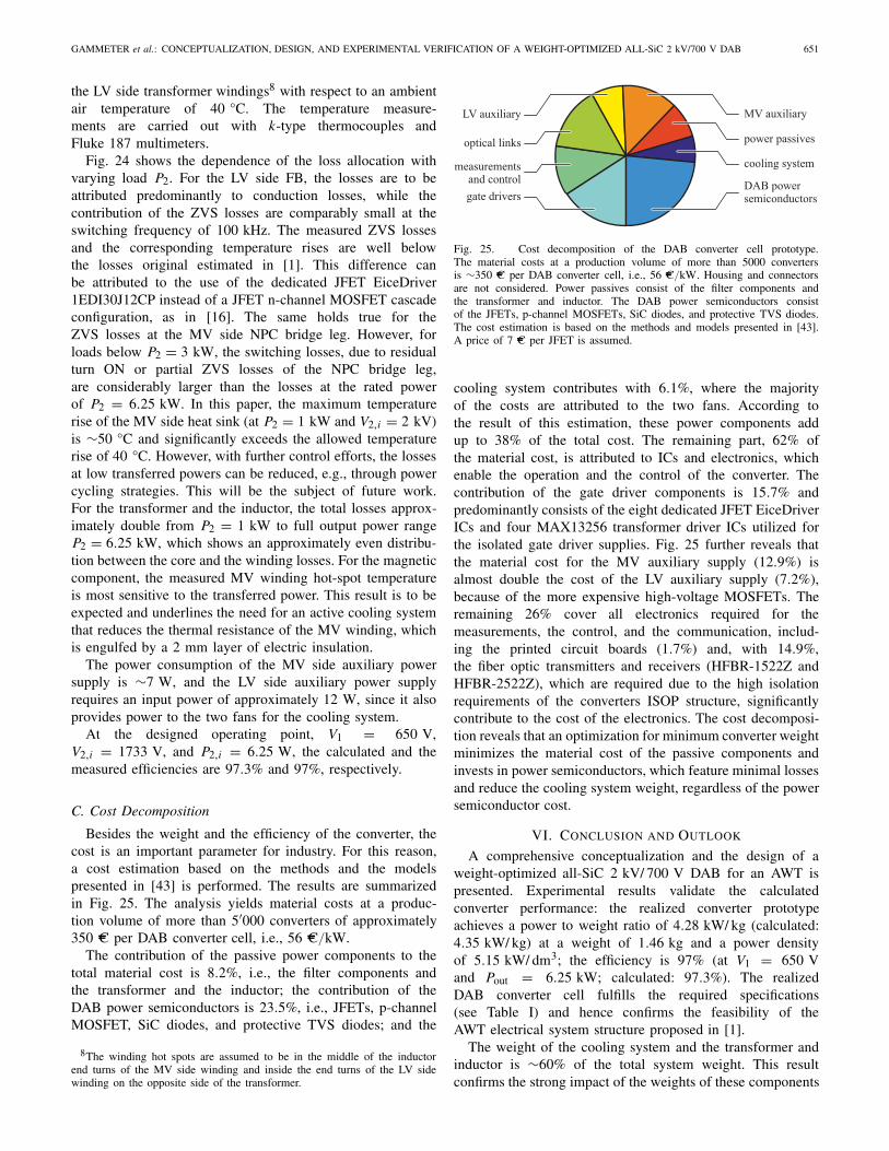
C. Cost Decomposition
Besides the weight and the efficiency of the converter, thecost is an important parameter for industry. For this reason,a cost estimation based on the methods and the modelspresented in [43] is performed. The results are summarizedin Fig. 25. The analysis yields material costs at a produc-tion volume of more than 5′000 converters of approximately350 C per DAB converter cell, i.e., 56 C/kW.
The contribution of the passive power components to thetotal material cost is 8.2%, i.e., the filter components andthe transformer and the inductor; the contribution of theDAB power semiconductors is 23.5%, i.e., JFETs, p-channelMOSFET, SiC diodes, and protective TVS diodes; and the
8The winding hot spots are assumed to be in the middle of the inductorend turns of the MV side winding and inside the end turns of the LV sidewinding on the opposite side of the transformer.
Fig. 25. Cost decomposition of the DAB converter cell prototype.The material costs at a production volume of more than 5000 convertersis ∼350 C per DAB converter cell, i.e., 56 C/kW. Housing and connectorsare not considered. Power passives consist of the filter components andthe transformer and inductor. The DAB power semiconductors consistof the JFETs, p-channel MOSFETs, SiC diodes, and protective TVS diodes.The cost estimation is based on the methods and models presented in [43].A price of 7 C per JFET is assumed.
cooling system contributes with 6.1%, where the majorityof the costs are attributed to the two fans. According tothe result of this estimation, these power components addup to 38% of the total cost. The remaining part, 62% ofthe material cost, is attributed to ICs and electronics, whichenable the operation and the control of the converter. Thecontribution of the gate driver components is 15.7% andpredominantly consists of the eight dedicated JFET EiceDriverICs and four MAX13256 transformer driver ICs utilized forthe isolated gate driver supplies. Fig. 25 further reveals thatthe material cost for the MV auxiliary supply (12.9%) isalmost double the cost of the LV auxiliary supply (7.2%),because of the more expensive high-voltage MOSFETs. Theremaining 26% cover all electronics required for themeasurements, the control, and the communication, includ-ing the printed circuit boards (1.7%) and, with 14.9%,the fiber optic transmitters and receivers (HFBR-1522Z andHFBR-2522Z), which are required due to the high isolationrequirements of the converters ISOP structure, significantlycontribute to the cost of the electronics. The cost decomposi-tion reveals that an optimization for minimum converter weightminimizes the material cost of the passive components andinvests in power semiconductors, which feature minimal lossesand reduce the cooling system weight, regardless of the powersemiconductor cost.
VI. CONCLUSION AND OUTLOOK
A comprehensive conceptualization and the design of aweight-optimized all-SiC 2 kV/ 700 V DAB for an AWT ispresented. Experimental results validate the calculatedconverter performance: the realized converter prototypeachieves a power to weight ratio of 4.28 kW/ kg (calculated:4.35 kW/ kg) at a weight of 1.46 kg and a power densityof 5.15 kW/ dm3; the efficiency is 97% (at V1 = 650 Vand Pout = 6.25 kW; calculated: 97.3%). The realizedDAB converter cell fulfills the required specifications(see Table I) and hence confirms the feasibility of theAWT electrical system structure proposed in [1].
The weight of the cooling system and the transformer andinductor is ∼60% of the total system weight. This resultconfirms the strong impact of the weights of these components
652 IEEE JOURNAL OF EMERGING AND SELECTED TOPICS IN POWER ELECTRONICS, VOL. 04, NO. 2, JUNE 2016
on the total system weight and justifies the reason for theweight optimization to focus on these components.
The switching losses are decreased (compared with [1])through the evolution of the SiC technology, i.e., due tothe JFET direct drive technology. This and the fact that thetransformer core material accounts for 31% of the total systemweight suggest that a DAB operated at a higher switchingfrequency may have the potential for a further weightreduction.
The MV winding is the first component to reach itsthermal limit, in spite of the fact, that the transformer coolingsystem accounts for 14% of the total system weight. Dueto this reason, different transformer topologies, which do notengulf the winding with a large thermal insulation, may allowfor a further weight reduction. Respective investigations andoptimizations are subject to future work.
The presented comprehensive weight-optimized design ofthe 6.25 kW DAB converter cell, used as part of a 25 kWISOP structured dc–dc converter, considers multiobjectiveoptimization and takes, besides the actual components weights,the losses of the converter components and the associatedweight of the required optimized cooling system into account.Furthermore, the weights of the additional circuitries requiredfor the converter operation and the integration into the finalelectrical AWT system, i.e., gate drivers, digital control,filters, and auxiliary power supplies, are also considered. Theconverter design detailed in this paper, thus points out thetechnological limits the DAB converter is subject to and isnot limited to the considered AWT application.
The weight optimization of components is of uttermostimportance for not only AWTs but for airborne applications ingeneral, since each additional kilogram of weight carried in anaircraft increases the fuel consumption by 2900 liter keroseneper year [44]. With respect to a power converter not only theweight of the power components but also efficiency plays amajor role, since the weight of the converters cooling systemincreases with increasing losses and, most often, substantiallycontributes to the total converter weight; from practicalexperience, it is estimated that 1 kW of losses involves 10 kgof secondary cooling equipment [46]. For this reason, thepresented design procedure has to be seen in a more generalcontext as guideline for the realization of lightweight powerconverters for airborne applications.
APPENDIX
DESIGN OF THE FILTER NETWORKS
The presented design approach employs the simplifieddynamic DAB converter model developed in [35] and thenetworks connected to the LV and the MV sides. Fig. 26shows the considered network, which consists of two currentsources to model the inner most part of the DAB converter,a LV side C LC filter with damping network, and, on theMV side, the equivalent sum of the MV filter capacitors, C2,and the equivalent circuits of the tether and the ground station,i.e., the rectifier/inverter system located on the ground, thatare relevant for a single DAB converter cell. For the groundstation, no weight limitation applies and, for this reason,a sufficiently large dc-link capacitance C3 at the ground station
Fig. 26. Equivalent circuit of the AWT power electronic system [1], includingthe simplified circuit model of the DAB presented in [35] (instead of theassumed ideal transformer in [1]).
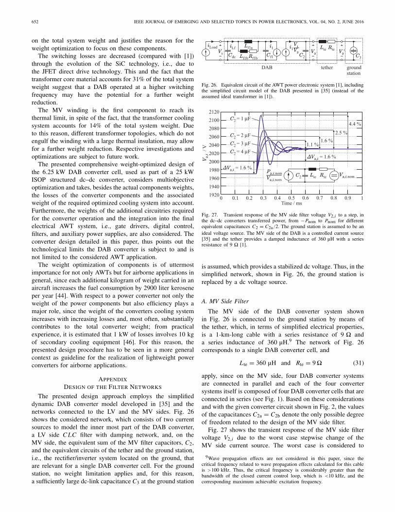
Fig. 27. Transient response of the MV side filter voltage V2,i to a step, inthe dc–dc converters transferred power, from −Pnom to Pnom for differentequivalent capacitances C2 = C2a/2. The ground station is assumed to be anideal voltage source. The MV side of the DAB is a controlled current source[35] and the tether provides a damped inductance of 360 µH with a seriesresistance of 9 � [1].
is assumed, which provides a stabilized dc voltage. Thus, in thesimplified network, shown in Fig. 26, the ground station isreplaced by a dc voltage source.
A. MV Side Filter
The MV side of the DAB converter system shownin Fig. 26 is connected to the ground station by means ofthe tether, which, in terms of simplified electrical properties,is a 1-km-long cable with a series resistance of 9 � anda series inductance of 360 µH.9 The network of Fig. 26corresponds to a single DAB converter cell, and
L te = 360 µH and Rte = 9 � (31)
apply, since on the MV side, four DAB converter systemsare connected in parallel and each of the four convertersystems itself is composed of four DAB converter cells that areconnected in series (see Fig. 1). Based on these considerationsand with the given converter circuit shown in Fig. 2, the valuesof the capacitances C2a = C2b denote the only possible degreeof freedom related to the design of the MV side filter.
Fig. 27 shows the transient response of the MV side filtervoltage V2,i due to the worst case stepwise change of theMV side current source. The worst case is considered to
9Wave propagation effects are not considered in this paper, since thecritical frequency related to wave propagation effects calculated for this cableis >100 kHz. Thus, the critical frequency is considerably greater than thebandwidth of the closed current control loop, which is <10 kHz, and thecorresponding maximum achievable excitation frequency.
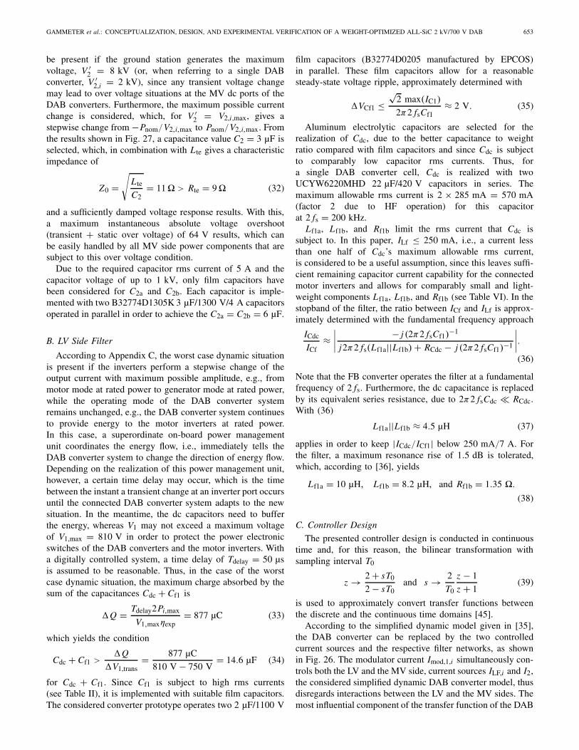
GAMMETER et al.: CONCEPTUALIZATION, DESIGN, AND EXPERIMENTAL VERIFICATION OF A WEIGHT-OPTIMIZED ALL-SiC 2 kV/700 V DAB 653
be present if the ground station generates the maximumvoltage, V ′
2 = 8 kV (or, when referring to a single DABconverter, V ′
2,i = 2 kV), since any transient voltage changemay lead to over voltage situations at the MV dc ports of theDAB converters. Furthermore, the maximum possible currentchange is considered, which, for V ′
2 = V2,i,max, gives astepwise change from −Pnom/V2,i,max to Pnom/V2,i,max. Fromthe results shown in Fig. 27, a capacitance value C2 = 3 µF isselected, which, in combination with L te gives a characteristicimpedance of
Z0 =√
L te
C2= 11 � > Rte = 9 � (32)
and a sufficiently damped voltage response results. With this,a maximum instantaneous absolute voltage overshoot(transient + static over voltage) of 64 V results, which canbe easily handled by all MV side power components that aresubject to this over voltage condition.
Due to the required capacitor rms current of 5 A and thecapacitor voltage of up to 1 kV, only film capacitors havebeen considered for C2a and C2b. Each capacitor is imple-mented with two B32774D1305K 3 µF/1300 V/4 A capacitorsoperated in parallel in order to achieve the C2a = C2b = 6 µF.
B. LV Side Filter
According to Appendix C, the worst case dynamic situationis present if the inverters perform a stepwise change of theoutput current with maximum possible amplitude, e.g., frommotor mode at rated power to generator mode at rated power,while the operating mode of the DAB converter systemremains unchanged, e.g., the DAB converter system continuesto provide energy to the motor inverters at rated power.In this case, a superordinate on-board power managementunit coordinates the energy flow, i.e., immediately tells theDAB converter system to change the direction of energy flow.Depending on the realization of this power management unit,however, a certain time delay may occur, which is the timebetween the instant a transient change at an inverter port occursuntil the connected DAB converter system adapts to the newsituation. In the meantime, the dc capacitors need to bufferthe energy, whereas V1 may not exceed a maximum voltageof V1,max = 810 V in order to protect the power electronicswitches of the DAB converters and the motor inverters. Witha digitally controlled system, a time delay of Tdelay = 50 µsis assumed to be reasonable. Thus, in the case of the worstcase dynamic situation, the maximum charge absorbed by thesum of the capacitances Cdc + Cf1 is
�Q = Tdelay2Pi,max
V1,maxηexp= 877 µC (33)
which yields the condition
Cdc + Cf1 >�Q
�V1,trans= 877 µC
810 V − 750 V= 14.6 µF (34)
for Cdc + Cf1. Since Cf1 is subject to high rms currents(see Table II), it is implemented with suitable film capacitors.The considered converter prototype operates two 2 µF/1100 V
film capacitors (B32774D0205 manufactured by EPCOS)in parallel. These film capacitors allow for a reasonablesteady-state voltage ripple, approximately determined with
�VCf1 ≤√
2 max(IC1)
2π2 fsCf1≈ 2 V. (35)
Aluminum electrolytic capacitors are selected for therealization of Cdc, due to the better capacitance to weightratio compared with film capacitors and since Cdc is subjectto comparably low capacitor rms currents. Thus, fora single DAB converter cell, Cdc is realized with twoUCYW6220MHD 22 µF/420 V capacitors in series. Themaximum allowable rms current is 2 × 285 mA = 570 mA(factor 2 due to HF operation) for this capacitorat 2 fs = 200 kHz.
Lf1a, Lf1b, and Rf1b limit the rms current that Cdc issubject to. In this paper, ILf ≤ 250 mA, i.e., a current lessthan one half of Cdc’s maximum allowable rms current,is considered to be a useful assumption, since this leaves suffi-cient remaining capacitor current capability for the connectedmotor inverters and allows for comparably small and light-weight components Lf1a, Lf1b, and Rf1b (see Table VI). In thestopband of the filter, the ratio between ICf and ILf is approx-imately determined with the fundamental frequency approach
ICdc
ICf≈
∣∣∣∣ − j (2π2 fsCf1)−1
j2π2 fs(Lf1a||Lf1b) + RCdc − j (2π2 fsCf1)−1
∣∣∣∣.(36)
Note that the FB converter operates the filter at a fundamentalfrequency of 2 fs. Furthermore, the dc capacitance is replacedby its equivalent series resistance, due to 2π2 fsCdc RCdc.With (36)
Lf1a||Lf1b ≈ 4.5 µH (37)
applies in order to keep |ICdc/ICf1| below 250 mA/7 A. Forthe filter, a maximum resonance rise of 1.5 dB is tolerated,which, according to [36], yields
Lf1a = 10 µH, Lf1b = 8.2 µH, and Rf1b = 1.35 �.
(38)
C. Controller Design
The presented controller design is conducted in continuoustime and, for this reason, the bilinear transformation withsampling interval T0
z → 2 + sT0
2 − sT0and s → 2
T0
z − 1
z + 1(39)
is used to approximately convert transfer functions betweenthe discrete and the continuous time domains [45].
According to the simplified dynamic model given in [35],the DAB converter can be replaced by the two controlledcurrent sources and the respective filter networks, as shownin Fig. 26. The modulator current Imod,1,i simultaneously con-trols both the LV and the MV side, current sources ILF,i and I2,the considered simplified dynamic DAB converter model, thusdisregards interactions between the LV and the MV sides. Themost influential component of the transfer function of the DAB

654 IEEE JOURNAL OF EMERGING AND SELECTED TOPICS IN POWER ELECTRONICS, VOL. 04, NO. 2, JUNE 2016
converter without filter networks, GDAB,0 = ILF,i/Imod,1,i ,identified in [35] is the time delay introduced by the digitalcontrol system, Tc = 50 µs
GDAB,0(s) = ILF,i
Imod,1,i= e−sTc (40)
and the total open-loop transfer function of a DAB convertercell, Gi,ol(s), is
Gi,ol(s) = ILF,i
Imod,1,i= ZCf1
ZLf1 + ZCf1GDAB,0,
ZLf1 = sLf1a(Rf1b + sLf1b)
sLf1a + (Rf1b + sLf1b), and ZCf1 = 1
sCf1.
(41)
The transfer functions of the Proportional Integral (PI)controllers are [35]
Gc = Kpz − (1 − Tc/Ti)
z − 1z→s= Kp
(1 − Tc
2Ti+ 1
sTi
)(42)
with gain Kp, integral time constant Ti, and controller updateperiod time Tc. The discrete time transfer function of a movingaverage filter of filter order Ns is
Havg = 1
Ns
Ns−1∑k=0
1
zkz→s= 1
Ns
Ns−1∑k=0
(2 − sTs
2 + sTs
)k
(43)
with Ns = 8 and Ts = 1.25 µs is applicable in this paper.Hence, the voltages V1 and V2,i and the filter currents ILF,iare sampled and averaged eight times within each switchingperiod.
In order to achieve a high bandwidth of the currentcontroller, and because the transfer function Gi,ol is essentiallya second-order low-pass filter with a time delay, the currentcontrollers are designed with the optimum amount methodwith a selected phase margin of ϕI = 60°. For this, the cornerfrequency of the current controller’s transfer function, fi,I =1/(2πTi,I), is set equal to the frequency, where Gi,ol showsmaximum resonant gain∣∣∣∣Gi,ol
(j
2π
Ti,I
)∣∣∣∣ = max∣∣Gi,ol
∣∣. (44)
The current controller gain Kp,I is adjusted to achieve a phasemargin of ϕI = 60 ° at the cross over frequency ωϕ,I of theloop gain
Fol,I = Gc,IGi,ol Havg (45)
by solving
� [Fol,I(jωϕ,I)|Kp,I→1] != ϕI − π (46)
in order to determine ωϕ,I and, subsequently∣∣Fol,I(jωϕ,I)∣∣ != 1 (47)
to determine Kp,I. The loop gain for the voltage controllerused to control V1 then becomes
Fol,V1 = Gc,V1Gcl,I Havg with Gcl,I = Fol,I
1 + Fol,I(48)
Fig. 28. Bode plots of the plant’s transfer function Gi,ol , the open-loop gainsFol,I, Fol,V1, and Fol,V2, and the closed-loop transfer functions Gcl,I, Gcl,V1,and Gcl,V2.
TABLE XI
DC–DC CONVERTER CONTROL PARAMETERS
L
i.e., Gcl,I is the transfer function of the closed currentcontrol loop. Fig. 28 shows all resulting open- and closed-loopgains.
The voltage controller of V1 stabilizes the voltage of thedc bus on the LV side and, for this purpose, alters thereference current ILF,ref. This voltage controller is designedwith the symmetric optimum method [35], for a phase marginof ϕV1 = 60 °. With this, the controller parametersKp,V1 = 44.1 mA/V and Tp,V1 = 5.83 ms result.
Finally, the voltage controllers for the MV side voltages ofthe slave modules, V2,2, V2,3, and V2,4, need to be designed.The MV side filter capacitors realize a capacitive voltagedivider, which enables voltage balancing in the case oftime varying output currents, i.e., ac currents. These voltagecontrollers, therefore, need to compensate unbalancing dueto slowly varying output current deviations of the differ-ent modules. For this reason, the respective closed-loopbandwidths can be set to a comparably low value
ωϕ,V2 = ωϕ,V2,2 = ωϕ,V2,3 = ωϕ,V2,4 = ωϕ,V1/10 (49)
i.e., an order of magnitude below ωϕ,V1 is selected(see Fig. 28), in order to avoid interactions between thevoltage controller used to stabilize V1 and the MV sidevoltage controllers. The controllers are designed accordingto the symmetric optimum method for a phase margin ofϕV1 = 60 °. Table XI summarizes the resulting controllerparameters.
GAMMETER et al.: CONCEPTUALIZATION, DESIGN, AND EXPERIMENTAL VERIFICATION OF A WEIGHT-OPTIMIZED ALL-SiC 2 kV/700 V DAB 655
REFERENCES
[1] J. W. Kolar et al., “Conceptualization and multi-objective optimizationof the electric system of an airborne wind turbine,” IEEE J. Emerg. Sel.Topics Power Electron., vol. 1, no. 2, pp. 73–103, Jun. 2013.
[2] J. Adhikary and S. K. Panda, “Generation and transmission of electricalenergy in high-altitude wind power generating system,” IEEE J. Emerg.Sel. Topics Power Electron., vol. 3, no. 2, pp. 459–470, Jun. 2015,doi: 10.1109/JESTPE.2015.2388702.
[3] E. Murtola, S. M. Neuhold, and P. Anliker, “Hyperelastic high voltageconductor for electric drilling,” in Proc. 4th Int. Conf. CMOO, Oct. 2005,pp. 1–11.
[4] S. M. Neuhold, “A hyper elastic conductor for bulk energy transfer inthe wall of spoolable tubes for electric deep drilling,” Ph.D. dissertation,Dept. Swiss Federal Inst. Technol. Zurich, ETH Zürich, Zürich,Switzerland, 2007.
[5] P. Ragot, M. Markovic, and Y. Perriard, “Optimization of electric motorfor a solar airplane application,” IEEE Trans. Ind. Appl., vol. 42, no. 4,pp. 1053–1061, Jul./Aug. 2006.
[6] Y. Perriard, P. Ragot, and M. Markovic, “Brushless DC motor optimiza-tion process—Choice between standard or straight tooth shape,” in Proc.41st IEEE Ind. Appl. Soc. Annu. Meeting, Tampa, FL, USA, Oct. 2006,pp. 1898–1904.
[7] P. Ragot, P. Germano, M. Markovic, and Y. Perriard, “Brushless DCmotor for a solar airplane application: Comparison between simulationsand measurements,” in Proc. IEEE Ind. Appl. Soc. Annu. Meeting,Edmonton, AB, Canada, Oct. 2008, pp. 1–6.
[8] M. van der Geest, H. Polinder, J. A. Ferreira, and D. Zeilstra, “Opti-mization and comparison of electrical machines using particle swarmoptimization,” in Proc. 20th IEEE Int. Conf. Elect. Mach. (ICEM),Marseille, France, Sep. 2012, pp. 1380–1386.
[9] M. van der Geest, H. Polinder, J. A. Ferreira, and D. Zeilstra,“Machine selection and initial design of an aerospace starter/generator,”in Proc. IEEE Int. Electr. Mach. Drives Conf. (IEMDC), May 2013,pp. 196–203.
[10] C. Gammeter, Y. Drapela, A. Tüysüz, and J. W. Kolar, “Weight opti-mization of a machine for airborne wind turbines,” in Proc. 40th Annu.Conf. IEEE Ind. Electron. Soc. (IECON), vol. 1. Dallas, TX, USA,Oct./Nov. 2014, pp. 950–958.
[11] J. Adhikari, A. K. Rathore, and S. K. Panda, “Modular interleaved soft-switching DC-DC converter for high-altitude wind energy application,”IEEE J. Emerg. Sel. Topics Power Electron., vol. 2, no. 4, pp. 727–738,Dec. 2014.
[12] S. Mounce, B. McPherson, R. Schupbach, and A. B. Lostetter, “Ultra-lightweight, high efficiency SiC based power electronic converters forextreme environments,” in Proc. IEEE Aerosp. Conf., Big Sky, MT, USA,Mar. 2006, doi: 10.1109/AERO.2006.1655979.
[13] J. Millan, P. Godignon, X. Perpina, A. Perez-Tomas, and J. Rebollo,“A survey of wide bandgap power semiconductor devices,” IEEE Trans.Power Electron., vol. 29, no. 5, pp. 2155–2163, May 2014.
[14] B. Wrzecionko, D. Bortis, and J. W. Kolar, “A 120 °C ambient tem-perature forced air-cooled normally-off SiC JFET automotive invertersystem,” IEEE Trans. Power Electron., vol. 29, no. 5, pp. 2345–2358,May 2014.
[15] M. Schweizer and J. W. Kolar, “Design and implementation of a highlyefficient three-level T-type converter for low-voltage applications,” IEEETrans. Power Electron., vol. 28, no. 2, pp. 899–907, Feb. 2013.
[16] R. A. Friedemann, F. Krismer, and J. W. Kolar, “Design of a minimumweight dual active bridge converter for an airborne wind turbine system,”in Proc. 27th Appl. Power Electron. Conf. Expo. (APEC), Orlando, FL,USA, Feb. 2012, pp. 509–516.
[17] D. Rothmund, G. Ortiz, T. Guillod, and J. W. Kolar, “10 kV SiC-basedisolated DC-DC converter for medium voltage-connected solid-statetransformers,” in Proc. 30th Appl. Power Electron. Conf. Expo. (APEC),Charlotte, NC, USA, Mar. 2015, pp. 1096–1103.
[18] M. R. Islam, G. Lei, Y. Guo, and J. Zhu, “Optimal design of high-frequency magnetic links for power converters used in grid-connectedrenewable energy systems,” IEEE Trans. Magn., vol. 50, no. 11,Nov. 2014, Art. ID 2006204.
[19] W. Water and J. Lu, “Shielding analysis of high-frequency coaxialtransformers used for electric vehicle on-board charging systems,” IEEETrans. Magn., vol. 49, no. 7, pp. 4005–4008, Jul. 2013.
[20] W. Wang, K. W. E. Cheng, K. Ding, and T. F. Chan, “A polymer-bonded magnetic core for high-frequency converters,” IEEE Trans.Magn., vol. 48, no. 11, pp. 4328–4331, Nov. 2012.
[21] R. A. Jabr, “Application of geometric programming to transformerdesign,” IEEE Trans. Magn., vol. 41, no. 11, pp. 4261–4269, Nov. 2005.
[22] G. Ortiz, M. Leibl, J. W. Kolar, and O. Apeldoorn, “Medium frequencytransformers for solid-state-transformer applications—Design and exper-imental verification,” in Proc. 10th IEEE Int. Conf. Power Electron.Drive Syst. (PEDS), Kitakyushu, Japan, Apr. 2013, pp. 1285–1290.
[23] G. Ortiz, J. Biela, and J. W. Kolar, “Optimized design of mediumfrequency transformers with high isolation requirements,” in Proc. 36thAnnu. Conf. IEEE Ind. Electron. Soc. (IECON), Phoenix, AZ, USA,Nov. 2010, pp. 631–638.
[24] T. Guillod, J. E. Huber, G. Ortiz, A. De, C. M. Franck, and J. W. Kolar,“Characterization of the voltage and electric field stresses in multi-cell solid-state transformers,” in Proc. IEEE Energy Convers. Congr.Expo. (ECCE), Pittsburgh, PA, USA, Sep. 2014, pp. 4726–4734.
[25] M. B. Dogruoz and M. Arik, “On the conduction and convection heattransfer from lightweight advanced heat sinks,” IEEE Trans. Compon.Packag. Technol., vol. 33, no. 2, pp. 424–431, Jun. 2010.
[26] P. Ning, F. Wang, and K. D. T. Ngo, “Forced-air coolingsystem design under weight constraint for high-temperatureSiC converter,” IEEE Trans. Power Electron., vol. 29, no. 4,pp. 1998–2007, Apr. 2014.
[27] C. Gammeter, F. Krismer, and J. W. Kolar, “Weight optimization ofa cooling system composed of fan and extruded fin heat sink,” IEEETrans. Ind. Appl., vol. 51, no. 1, pp. 509–520, Jan./Feb. 2015.
[28] F. Krismer and J. W. Kolar, “Closed form solution for minimumconduction loss modulation of DAB converters,” IEEE Trans. PowerElectron., vol. 27, no. 1, pp. 174–188, Jan. 2012.
[29] F. Krismer and J. W. Kolar, “Accurate power loss model derivation of ahigh-current dual active bridge converter for an automotive application,”IEEE Trans. Ind. Electron., vol. 57, no. 3, pp. 881–891, Mar. 2010.
[30] J. Everts, F. Krismer, J. Van den Keybus, J. Driesen, and J. W. Kolar,“Charge-based ZVS soft switching analysis of a single-stage dualactive bridge AC-DC converter,” in Proc. IEEE Energy Convers. Congr.Expo. (ECCE), Denver, CO, USA, Sep. 2013, pp. 4820–4829.
[31] R. Kotte, E. Gockenbach, and H. Borsi, “About the breakdown andpartial discharge behavior of different heat-resistant cast resins,” inProc. 6th Int. Conf. Properties Appl. Dielectr. Mater., vol. 2. 2000,pp. 583–586.
[32] A. Kaindl, L. Schön, R. Röckelein, and H. Borsi, “Influence ofprocessing parameters on electrical insulation properties for epoxy-resinmaterials-an investigation by experiment and finite element analysissimulation,” in Proc. Conf. Rec. IEEE Int. Symp. Elect. Insul., Apr. 2000,pp. 48–51.
[33] M. Beyer, W. Boeck, K. Möller, and W. Zaengl, Hochspannungstechnik.Berlin, Germany: Springer-Verlag, 1986.
[34] R. Schifani and V. Gagliardo, “Partial discharge patterns and agingphenomena at different temperatures in filled and unfilled epoxy,by a modified CIGRE setup, method I,” in Proc. IEEE 5th Int.Conf. Conduction Breakdown Solid Dielectr. (ICSD), Jul. 1995,pp. 329–333.
[35] F. Krismer and J. W. Kolar, “Accurate small-signal model for the digitalcontrol of an automotive bidirectional dual active bridge,” IEEE Trans.Power Electron., vol. 24, no. 12, pp. 2756–2768, Dec. 2009.
[36] R. W. Erickson, “Optimal single resistors damping of input filters,” inProc. 14th Appl. Power Electron. Conf. Expo. (APEC), vol. 2. Dallas,TX, USA, Mar. 1999, pp. 1073–1079.
[37] K. H. Edelmoser, H. Ertl, and F. Zach, “A multi-cell switch-mode power-supply concept featuring inherent input voltage balancing,” in Proc. 10thWSEAS Int. Conf. Circuits, Syst., Commun. Comput. (CSCC), Athens,Greece, Jul. 2006, pp. 201–206.
[38] M. Kasper, D. Bortis, and J. W. Kolar, “Novel high voltage conversionratio ‘Rainstick’ DC/DC converters,” in Proc. IEEE Energy Convers.Congr. Expo. (ECCE), Denver, CO, USA, Sep. 2013, pp. 789–796.
[39] R. L. Steigerwald, “A review of soft-switching techniques in highperformance DC power supplies,” in Proc. IEEE 21st Int. Conf. Ind.Electron., Control, Instrum. (IECON), vol. 1. Nov. 1995, pp. 1–7.
[40] STMicroelectronics. Data Sheet, STB20NM60-1—STP20NM60FP—STB20NM60—STP20NM60—STW20NM60, Revision 12 1/18. [Online].Available: http://www.st.com/, accessed Feb. 2015.
[41] L. Dalessandro, F. da Silveira Cavalcante, and J. W. Kolar, “Self-capacitance of high-voltage transformers,” IEEE Trans. Power Electron.,vol. 22, no. 5, pp. 2081–2092, Sep. 2007.
[42] H. Ertl, T. Wiesinger, and J. W. Kolar, “Active voltage balancing ofDC-link electrolytic capacitors,” IET Power Electron., vol. 1, no. 4,pp. 488–496, Dec. 2008.
[43] R. Burkart and J. W. Kolar, “Component cost models for multi-objectiveoptimizations of switched-mode power converters,” in Proc. IEEEEnergy Convers. Congr. Expo. (ECCE), Denver, CO, USA, Sep. 2013,pp. 2139–2146.

656 IEEE JOURNAL OF EMERGING AND SELECTED TOPICS IN POWER ELECTRONICS, VOL. 04, NO. 2, JUNE 2016
[44] C. Soutis, “Fibre reinforced composites in aircraft construction,” Progr.Aerosp. Sci., vol. 41, no. 2, pp. 143–151, 2005.
[45] A. V. Oppenheim and R. W. Schafer, Discrete-Time Signal Processing,3rd ed. Delhi, India: Pearson Higher Education, Aug. 2009.
[46] H. P. Feustel and J. Koszescha, “ECPE-roadmap 2025 automotive& aerospace power electronics,” in Proc. ECPE Roadmap Workshop,Munich, Germany, Mar. 2015.
Christoph Gammeter (S’13) received theM.Sc. degree from the Swiss Federal Institute ofTechnology (ETH) Zurich, Zürich, Switzerland,in 2012, where he is currently pursuing thePh.D. degree with the Power Electronics SystemsLaboratory.
He is with ETH Zurich, where he is involved inweight-optimized converters.
Florian Krismer (S’05–M’12) received theM.Sc. degree from the Vienna Universityof Technology, Vienna, Austria, in 2004, andthe Ph.D. degree from the Power ElectronicSystems Laboratory, Swiss Federal Institute ofTechnology (ETH) Zurich, Zürich, Switzerland,in 2011.
He is currently a Post-Doctoral Fellow with thePower Electronic Systems Laboratory, ETH Zurich.His current research interests include the analysis,design, and optimization of high-current and
high-frequency power converters.
Johann W. Kolar (F’10) received the M.Sc. andPh.D. (summa cum laude) degrees from the ViennaUniversity of Technology, Vienna, Austria.
He is currently a Full Professor and the Head ofthe Power Electronic Systems Laboratory with theSwiss Federal Institute of Technology (ETH) Zurich,Zürich, Switzerland. He has authored over 600 scien-tific papers in international journals and conferenceproceedings, and has filed over 100 patents. Hiscurrent research interests include ultracompact andultraefficient converter topologies, employing latest
power semiconductor technology, such as SiC and GaN, solid-state transform-ers, power supplies on chip, and ultrahigh speed and bearingless motors.
Dr. Kolar has proposed numerous novel pulsewidth modulation convertertopologies, and modulation and control concepts, such as the Vienna Rectifier,the Swiss Rectifier, and the Three-Phase AC-AC Sparse Matrix Converter. Hereceived nine IEEE TRANSACTIONS Prize Paper Awards, eight IEEE Con-ference Prize Paper Awards, the SEMIKRON Innovation Award in 2014, andthe ETH Zurich Golden Owl Award 2011 for Excellence in Teaching.