Embed Size (px)
Citation preview

Computation and measurement of aberrations in low energy
electron microscopy
Rudolf M Tromp
IBM T.J. Watson Research Center, Yorktown Heights, NY 10598
Kamerlingh Onnes Laboratory, Leiden University, The Netherlands

IBM/SPEC (AC)-LEEM/PEEM Design: ~30 instruments sold
gun
condenser
lenses
prism
array
projector
lenses
objective
lens
sample
screen
R.M.Tromp, M. Mankos, M.C. Reuter, A.W. Ellis, M. Copel
Surface Review and Letters 5 , 1189 (1998)
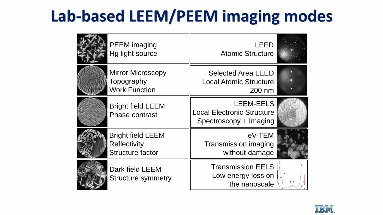
Lab-based LEEM/PEEM imaging modes
Selected Area LEED
Local Atomic Structure
200 nm
Dark field LEEM
Structure symmetry
Mirror Microscopy
Topography
Work Function
PEEM imaging
Hg light source
LEED
Atomic Structure
LEEM-EELS
Local Electronic Structure
Spectroscopy + Imaging
Bright field LEEM
Phase contrast
Bright field LEEM
Reflectivity
Structure factor
Transmission EELS
Low energy loss on
the nanoscale
eV-TEM
Transmission imaging
without damage

Lab-based LEEM/PEEM imaging modes
ARRES
Empty state
band structure
SPA-LEED-PLD
Atomic Layer Oscillations
during PLD growth
LEEM potentiometry
Contact-less nanoscale
device measurements
LEEM lithography
Structure fabrication
with few eV electrons
CBED
Local Atomic and
Electronic structure
SPA-LEED
Local strain
measurement
PEEM-ARPES
Filled state
band structure
LEEM-IV Imaging
Local Atomic Structure
2-5 nm
SPLEEM
Magnetic domain
imaging
IV-SPLEEM
Magnetic quantum
Well asymmetry

Synchrotron-based PEEM imaging modes
Picosecond
Resolution
Imaging
Linear Magnetic
Dichroism
Antiferromagnetism
PEEM-IV Imaging
20 nm resolution
Local chemistry
Dynamic Imaging
In-situ processing
Elemental/chemical
Cryo-PEEM
Solid State
Bio, soft matter
Localized Spectroscopy
Elemental, chemical
Magnetic, Valence
Circular Magnetic
Dichroism
Ferromagnetism
Valence Band Imaging
Surface, bulk
Topological
Biological Imaging
Organic, Inorganic
Elemental, chemical
Plasmonics
Dynamics, geometry

5 mm
BL
ML
Buffer
IBM/SPECS PEEM with an integrated imaging energy analyser: ARPES
R. M. Tromp et al., J. Phys. Cond. Matter 21 314007 (2009)
Epitaxial Graphene/6H-SiC(0001)Magnetic prism
Entrance slit
Objective
Sample
Selected area aperture
Contrast aperture
MCP screen
Dark-field imaging with bands
5 mm
BLML
min max
min maxReal spacek-space
Søren Ulstrup
Eli Rotenberg

J. Jobst, J. Kautz, D. Geelen, R.M. Tromp, S.J. van der MolenNature Comm. 6, 8926 (2015)
ARRESAngle ResolvedReflectedElectronSpectroscopy
H. Hibino et al.PRB 77 (2008) 075413

Empty State Bands Bulk hBN
J. Jobst, A. v.d. Torren, E. Krasovski, J. Bagley, C.R. Dean, R.M. Tromp, S.J. v.d. Molen

ARPES and ARRES for graphite and hBN
J. Jobst, A. v.d. Torren, E. Krasovskii, J. Bagley, C.R. Dean, R.M. Tromp, S.J. v.d. Molen, Nature communications 7 (2016) 13621
ARRES
ARPES
Eugene Krasovskii(Trieste, 2008)
hBN 12 eV
Complex bandstructureplus electron scatting
Single pixel in image: 10 nm

‘Instead of angular scan of a parallel beam, why not use a convergent beam?’ asked Frank Meyer zu Heringdorf
Jian-Min ZuoCBED 100 keV
Frank Meyer zu Heringdorf et al.CB-LEED for Graphene on Pt(111)
Spherical aberration limits spot size

Ronchigrams in LEEM
Real space
(0,0)
(1,0)
SE
CB-LEED, ronchigram, diffraction plane
8 mrad< ~100 nm
Overexposed central spot
Underexposed surroundingsSpot diameter < 100 nm
real space
real space
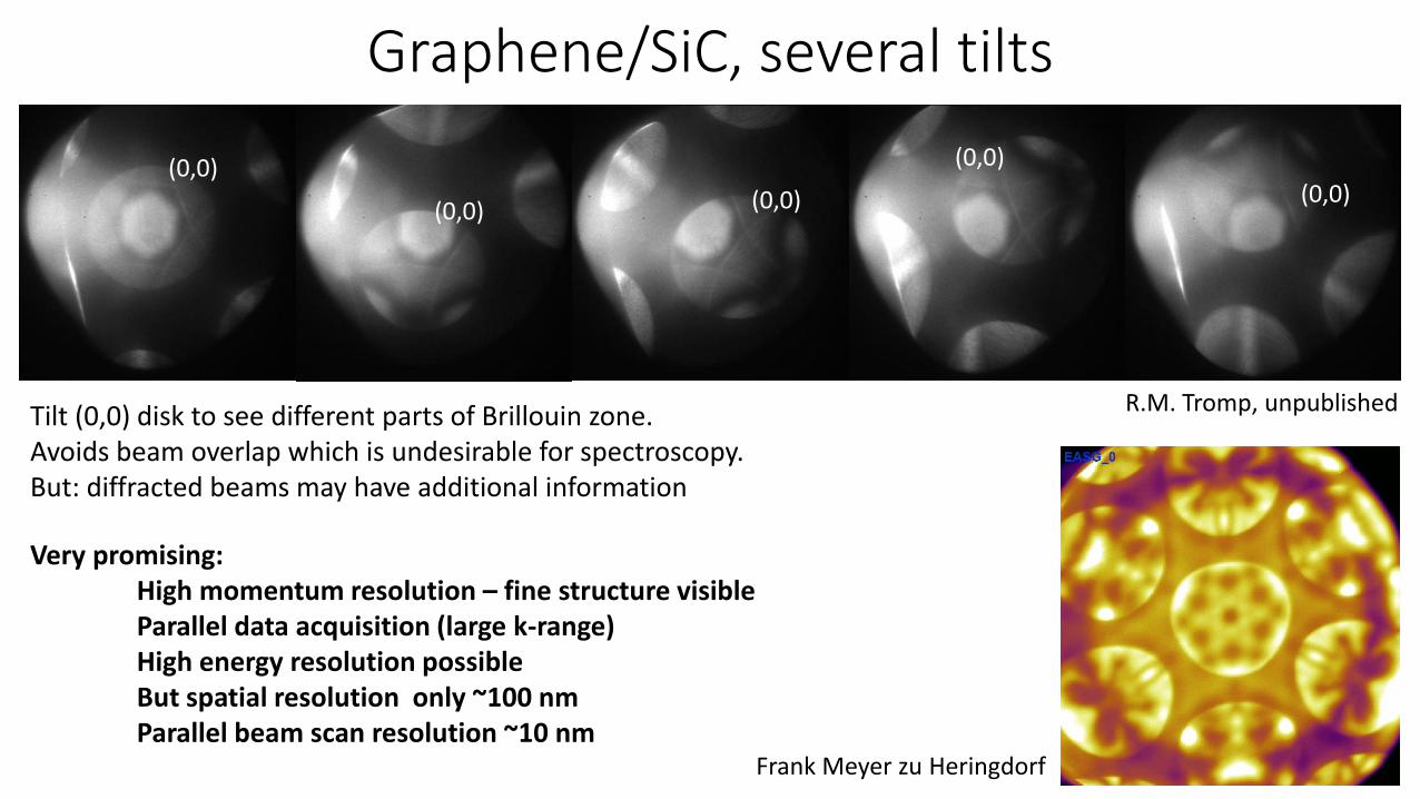
Graphene/SiC, several tilts
Tilt (0,0) disk to see different parts of Brillouin zone.Avoids beam overlap which is undesirable for spectroscopy.But: diffracted beams may have additional information
(0,0)(0,0)
(0,0)
(0,0)
(0,0)
R.M. Tromp, unpublished
Frank Meyer zu Heringdorf
Very promising:High momentum resolution – fine structure visibleParallel data acquisition (large k-range)High energy resolution possibleBut spatial resolution only ~100 nmParallel beam scan resolution ~10 nm

𝐾 Γ 𝑀
CB-LEED/ARRES: Conduction-electron
Band structure
CBED/ARPES/ARRES
CBED: Valence-electron density
J.M
. Zu
o, M
. Kim
, M. O
’Kee
ffe,
J. S
pen
ceD
irec
t o
bse
rvat
ion
of
d-o
rbit
al h
ole
s in
Cu
-Cu
bo
nd
ing
in C
u2O
NA
TUR
E 4
01
(1
99
9)
49
-52
ARPES:Valence-electronBand structure

Aberration Correction in Electron Optics:Walter Henneberg / Alfred Recknagel 1937

US Patent
7348566
R.M
. T
rom
p,
J.B
. H
annon
, A
.W.
Elli
s, W
. W
an, A
. B
erg
haus,
O.
Sch
aff,
Ultra
m.
11
0(2
01
0)
85
2-8
61
C3 = -Cc = L√(E/E0)
Aberrations strongly energy dependent
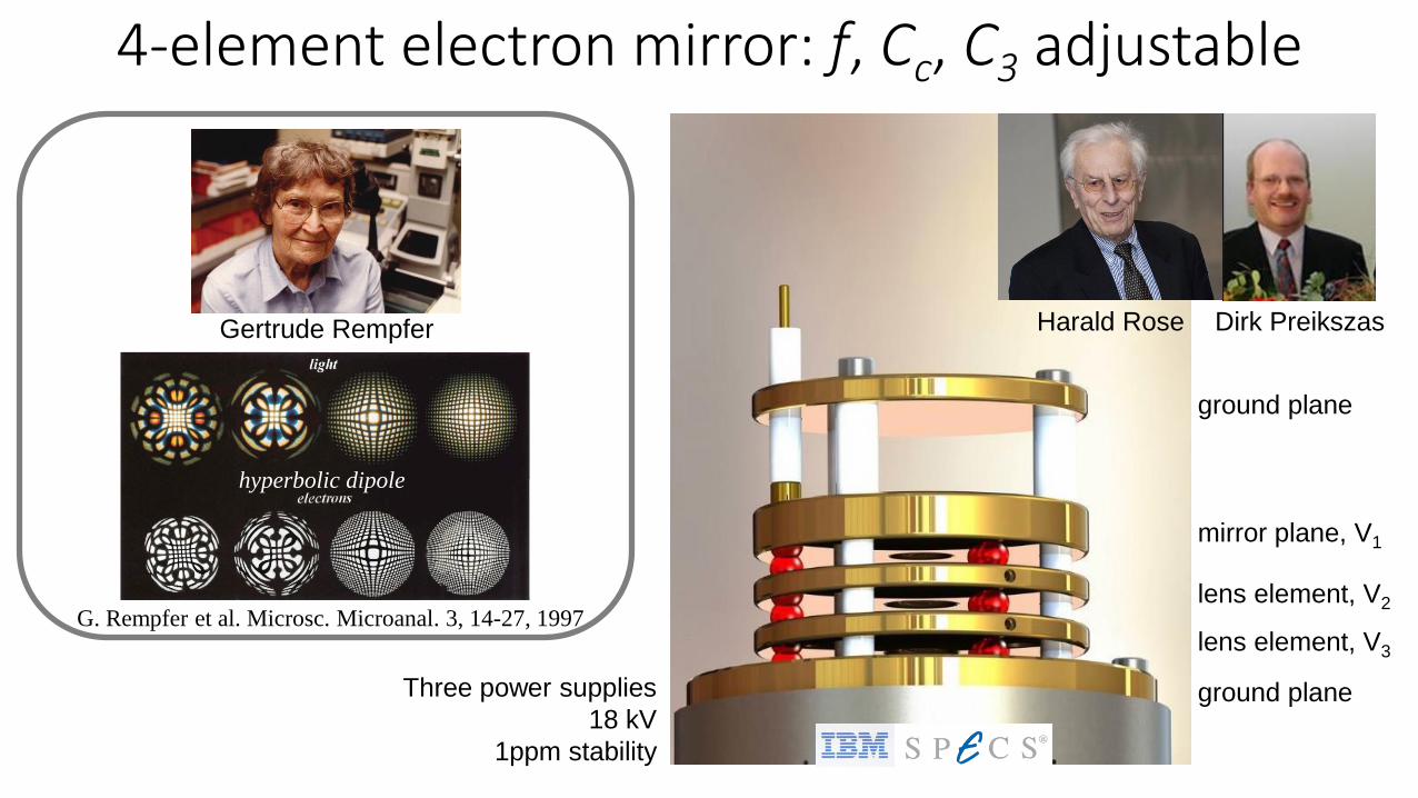
4-element electron mirror: f, Cc, C3 adjustable
Gertrude Rempfer
G. Rempfer et al. Microsc. Microanal. 3, 14-27, 1997
ground plane
lens element, V3
ground plane
mirror plane, V1
lens element, V2
Three power supplies
18 kV
1ppm stability
Harald Rose Dirk Preikszas
hyperbolic dipole

D Preikszas -3.1936 -0.11646 -531.8 -8.747E5 -9.62
B Lencova -3.1936 -0.12008 -495 -1.18E6 -9.60
B Lencova/J Zlamal -3.1936 -487 -1.29E6
E Munro et al 1995 -3.1936 -667 -28.7E6 -8.40
FiniteDifference
BEM
Author(s) Voltage image Z C3 C5 Cc
CPO 'benchmark‘ -3.198593 -0.119994(2) -532.37(6) -8.90(3)E5 -9.623(4)
D Preikszas -3.198593 -0.120000 -532.9 -8.743E5 -9.62
R Tromp (Munro) -3.198612 -0.120000 -532.89 -8.737E5 -9.624
Boundary Element vs. Finite Difference
Source: CPO user manual, xmpl2d17, mirror with negative aberrations, Frank Read

◘ ◘◘
◘
◘
◘
◘◘
◘ ◘ ◘◘◘ ◘ ◘ ◘◘
◘
◘
◘ ◘ ◘ ◘◘
◘
◘
◘ ◘ ◘ ◘◘
◘
◘
◘ ◘ ◘ ◘◘
◘
◘
◘
◘
◘ ◘◘
◘◘ ◘ ◘ ◘
◘
◘
◘
◘◘ ◘◘ ◘
◘
◘
◘ ◘ ◘ ◘◘
◘◘
◘
◘ ◘◘
◘
◘ ◘ ◘◘
◘
◘ ◘◘
◘
◘
◘ ◘◘
◘◘ ◘
◘
◘
● ● ●●
●
●
● ● ●●
●●
● ● ● ●●
●
●
● ● ● ● ●●
●
● ● ● ● ●●
●● ● ● ● ● ●
●● ● ● ● ●
●●
● ● ● ● ●●
●
● ● ● ● ●●
● ● ● ●●
● ●
●● ● ●
●●●
●●●
●●● ●
● ● ● ● ●
● ● ●
●V3-V2=7000
V3-V2=0
V1=-1200
V1=-1800
-4E3
0
2E3
-2E3
Cs
(m)
-Cc (m)
◘●
V1=-1200
V1=-1800
0 10 20 30
Correlation of first and higher order properties
focus aberrations
R.M. Tromp, J.B. Hannon, A.W. Ellis, W. Wan, A. Berghaus, O. Schaff, Ultram. 110 (2010) 852
d=
17
5 m
m
object/image
1% error 50-100% error

First order properties, first order of business
Adjustable parameter:
V1 offset of 10 V
(out of 16500, i.e. 0.06% )
V1=-1800
V1=-1200
TEM Grid
R.M
. Tro
mp, J
.B. H
annon, W
. Wan, A
. Berg
haus, O
. Schaff,
Ultra
mic
roscopy
http
://dx.d
oi.o
rg/1
0.1
016/j.u
ltram
ic.2
012.0
7.0
16

To correct we must measure
But what?
And how?
Heike Kamerlingh Onnes:
‘Door meten tot weten’

Diffracted (LEED) beams
C3 > 0 displacements linear +cubic
Si(111)(7x7) 5.4 eV
In practice change defocus:
d = C1.a + C3.a3
A. Berghaus O. Schaff J. Hannon
R.M. Tromp, J.B. Hannon, W. Wan, A. Berghaus, O. Schaff,
Ultramicroscopy http://dx.doi.org/10.1016/j.ultramic.2012.07.016
Direct visualization of C3 using micro-illumination

R.M. Tromp, J.B. Hannon, W. Wan, A. Berghaus, O. Schaff,
Ultramicroscopy http://dx.doi.org/10.1016/j.ultramic.2012.07.016
Measurement and Correction of C3

mirror
cathode lens
An achromat for photons…… and electrons?
dense flint
crown
??
Cc = -L√(E/E0)

mirror dispersion (Ccc)
Chromatic aberration of the mirror is not constant
MIRDA -MEBS

How to measure chromatic aberration?
E+E0E0
+
cath
od
e
ano
de
len
s
Defocus changes with take-off energy E0, and with final energy E+E0, both.

Three options:1. Gun voltage (E+E0) constant, change sample voltage: changes E0, but not E+E0
Measures uniform field aberration only, not magnetic lens, not electron mirror2. Use photoelectrons, change sample bias: changes E, but not E0
Measures magnetic lens and mirror, but not uniform field3. Change gun voltage, sample bias constant: changes both E0 and E+E0
Measures all threeBUT: also changes deflection angles through prism arrays and sample illuminationMUST adjust illumination for each data point + large off-axis aberrations in mirror path
How to measure chromatic aberration?
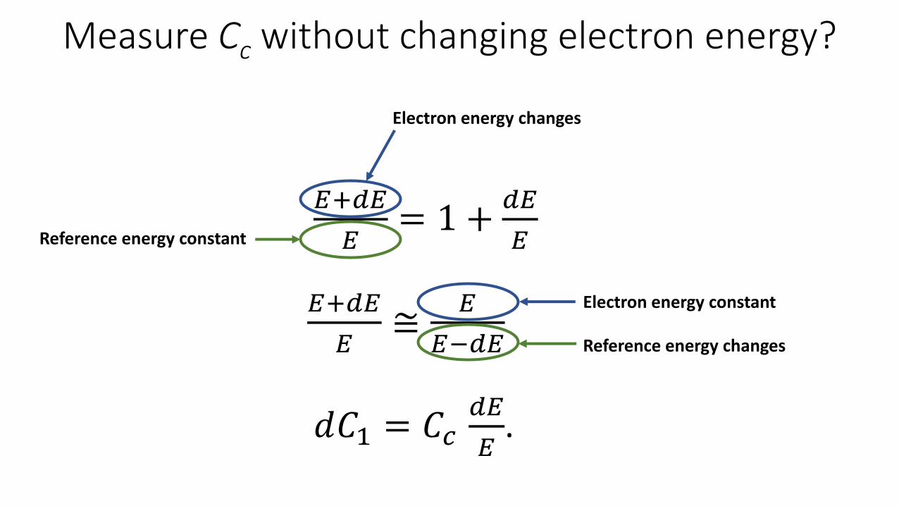
𝐸+𝑑𝐸
𝐸= 1 +
𝑑𝐸
𝐸
𝑑𝐶1 = 𝐶𝑐𝑑𝐸
𝐸.
𝐸+𝑑𝐸
𝐸≅
𝐸
𝐸−𝑑𝐸
Electron energy constant
Reference energy changes
Electron energy changes
Reference energy constant
Measure Cc without changing electron energy?

Reference energy = nominal column energyAll focal lengths are fixed relative to the nominal column energy.
Now:- Keep electron energy fixed (no problems with alignment)- Change reference energy, but keep all focal lengths constant for the reference energy.
𝒅𝑽
𝑽=
𝒅𝑬
𝑬(electrostatic lenses and electron mirror elements)
𝒅𝑰
𝑰=
𝟏
𝟐
𝒅𝑬
𝑬(magnetic lenses)
Measure Cc without changing electron energy?

Raytracing (MEBS):
Change electron energy
Change reference energy
Correct for objective lens reference excitation
= to better than 1:105
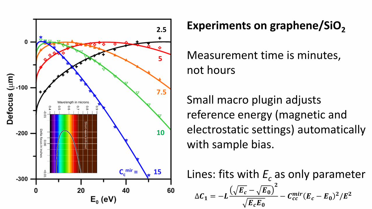
∆𝑪𝟏 = −𝑳𝑬𝒄 − 𝑬𝟎
𝟐
𝑬𝒄𝑬𝟎− 𝑪𝒄𝒄
𝒎𝒊𝒓 𝑬𝒄 − 𝑬𝟎𝟐/𝑬𝟐
A little trick to measure Cc with fixed electron energy
Ccmir = 15
7.5
5
2.5
10
Experiments on graphene/SiO2
Measurement time is minutes,not hours
Small macro plugin adjusts reference energy (magnetic and electrostatic settings) automatically with sample bias.
Lines: fits with Ec as only parameter
∆𝑪𝟏 = −𝑳𝑬𝒄 − 𝑬𝟎
𝟐
𝑬𝒄𝑬𝟎− 𝑪𝒄𝒄
𝒎𝒊𝒓 𝑬𝒄 − 𝑬𝟎𝟐/𝑬𝟐

Mirror Optics Mirrors :- Have been around a long time (Recknagel)- Can correct Cc, C3, (C5)- Are very compact compared to multipole optics- Are used successfully in LEEM/PEEM, SEM- Have promise for LV-TEM- Are relatively poorly understood- But raytracing has excellent predictive value
If we learn how to control dispersion (Ccc),
then we can make a PEEM apochromat
(resolution 2x, transmission 10x).
Maybe the most poorly understood
component in electron optics
CHANGE SIGN

Does the shape of the mirror matter?
Not here….

Does the shape of the mirror matter?
…or here….

The reflecting equipotential is far away, and can be either concave or convex…
How to design for desired properties? Can we flip the sign of Ccc?

Jim HannonArt Ellis
Weishi Wan
Johannes JobstTobias de JongDaniel Geelen
Sense Jan van der Molen
Oliver SchaffAlexander Kaiser
Andreas Berghaus
Eugene Krasovksii
Frank Meyer zu Heringdorf
Mark Reuter2017 AVS Hanyo Award
Arthur Ellis2010 AVS Hanyo Award

(a) (b) (c)
When, at the court of Chou, he first inspected the ancestral shrines and the arrangements for the great annual sacrifices to Heaven and Earth, he exclaimed: “As we use a glass to examine the forms of things, so must we study the past to understand the present.” (said about Confucius 551–479 BC)
Relevant geometric and chromatic aberrations

IV scan in Convergent Beam
Data set: ZBVH
• Convergent Beam Diffraction• Graphene / Ir(111)• Incident electron beam is
made convergent• LEED Spots fill entire screen
(and overlap)
• Works With and WithoutEnergy Filtering
• This series is without energy filtering, as can be judged by the secondaries that disperse to the left of the picture at about STV=6 eV
Frank Meyer zu Heringdorf et al.
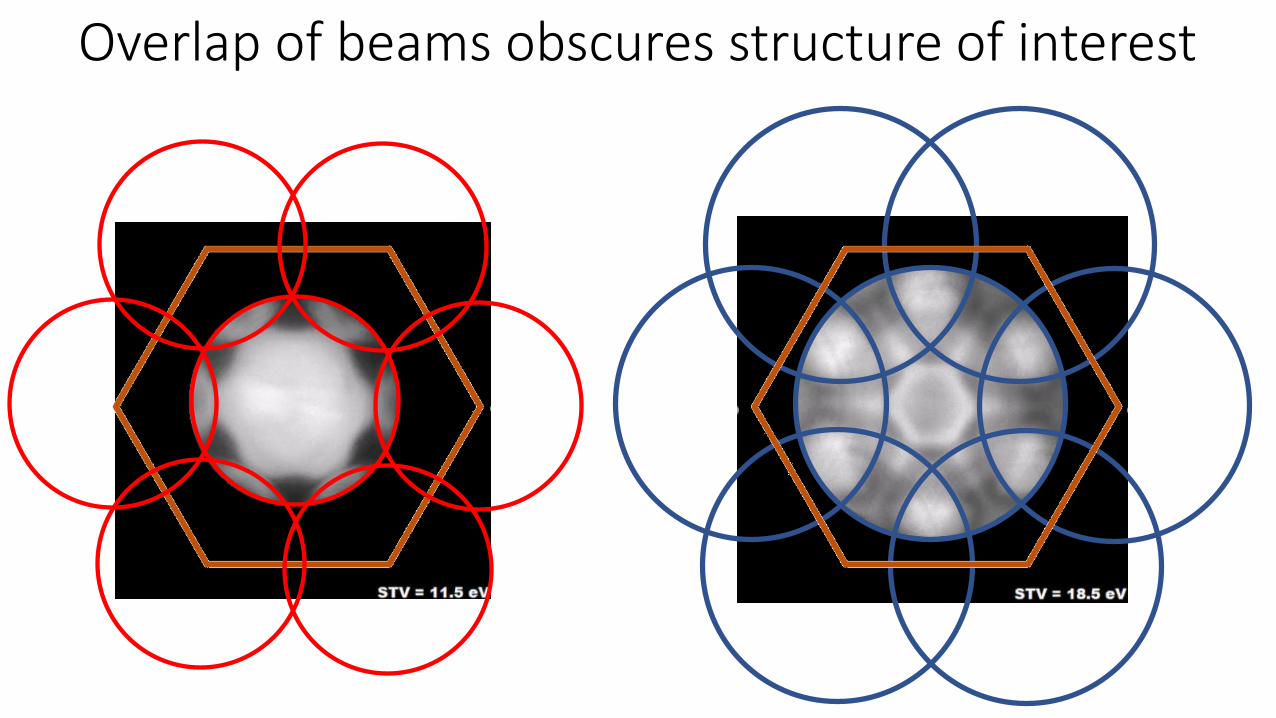
Overlap of beams obscures structure of interest