Embed Size (px)
Citation preview
Application ReportSLOA044 - March 2000
1
Conditioning a Switch-Mode Power SupplyCurrent Signal Using TI OP Amps
Larry Spaziani AAP Precision Analog
ABSTRACT
The switch-mode power supply primary current is often sensed using a power resistor. Using an opamp to amplify the current-sense signal can reduce cost and improve noise performance andefficiency. This report reviews the advantages of using an op amp circuit and analyzes the designcriteria needed to choose the proper op amp.
Contents
Introduction 2. . . . . . . . . . . . . . . . . . . . . . . . . . . . . . . . . . . . . . . . . . . . . . . . . . . . . . . . . . . . . . . . . . . . . . . . . . . . . Circuit Design 3. . . . . . . . . . . . . . . . . . . . . . . . . . . . . . . . . . . . . . . . . . . . . . . . . . . . . . . . . . . . . . . . . . . . . . . . . . . Advantages 4. . . . . . . . . . . . . . . . . . . . . . . . . . . . . . . . . . . . . . . . . . . . . . . . . . . . . . . . . . . . . . . . . . . . . . . . . . . . . . Choosing the Op Amp 5. . . . . . . . . . . . . . . . . . . . . . . . . . . . . . . . . . . . . . . . . . . . . . . . . . . . . . . . . . . . . . . . . . . . Conclusion 7. . . . . . . . . . . . . . . . . . . . . . . . . . . . . . . . . . . . . . . . . . . . . . . . . . . . . . . . . . . . . . . . . . . . . . . . . . . . . .
List of Figures
1 Typical Rsense Method and Proposed Op-Amp Method for Sensing PrimarySide Switch Current 2. . . . . . . . . . . . . . . . . . . . . . . . . . . . . . . . . . . . . . . . . . . . . . . . . . . . . . . . . . . . . . . . . . .
2 Current Sense Waveforms 6. . . . . . . . . . . . . . . . . . . . . . . . . . . . . . . . . . . . . . . . . . . . . . . . . . . . . . . . . . . . . . .
List of Tables
1 Suggested Texas Instruments Op Amps for Current Sensing 7. . . . . . . . . . . . . . . . . . . . . . . . . . . . . . . . . .
SLOA044
2 Conditioning a Switch-Mode Power Supply Current Signal Using TI OP Amps
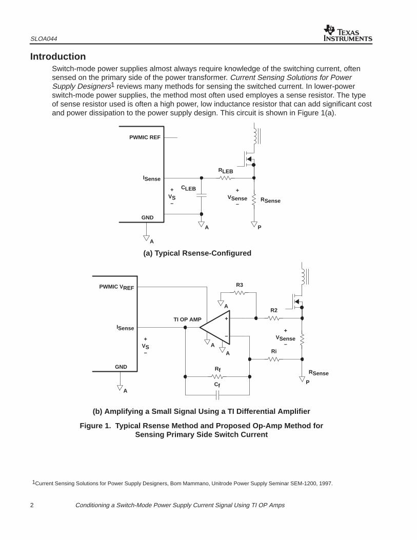
IntroductionSwitch-mode power supplies almost always require knowledge of the switching current, oftensensed on the primary side of the power transformer. Current Sensing Solutions for PowerSupply Designers1 reviews many methods for sensing the switched current. In lower-powerswitch-mode power supplies, the method most often used employes a sense resistor. The typeof sense resistor used is often a high power, low inductance resistor that can add significant costand power dissipation to the power supply design. This circuit is shown in Figure 1(a).
(b) Amplifying a Small Signal Using a TI Differential Amplifier
(a) Typical Rsense-Configured
ISense
PWMIC REF
GND
+VS–
RLEB
CLEB
RSense
+VSense
–
A
PA
–
+
ISense
PWMIC VREF
GND
+VS–
R2
Cf
RSense
+VSense
–
A
P
Ri
TI OP AMP
Rf
A
A
R3
A
Figure 1. Typical Rsense Method and Proposed Op-Amp Method forSensing Primary Side Switch Current
1Current Sensing Solutions for Power Supply Designers, Bom Mammano, Unitrode Power Supply Seminar SEM-1200, 1997.
SLOA044
3 Conditioning a Switch-Mode Power Supply Current Signal Using TI OP Amps
To overcome the cost and power dissipation of such power resistors, the circuit of Figure 1(b) isproposed. Using a differential amplifier made up of a low-power op amp and discrete resistorscan result in several advantages including lower power dissipation (efficiency), noise immunity,cost, and programmability.
Circuit Design
A switch-mode power supply often switches current on the primary side of a transformer througha MOSFET and measures the primary current with a sense resistor (Rsense) as shown inFigure 1(a). The pulse width modulator IC (PWM) usually requires a current-sense signal (Vs) inorder to provide short-circuit protection or for use in current mode control, or for both protectionand control. The peak value of Vs depends on the PWM IC used, but it is typically 1 volt.
The value of the sense resistor Rsense in Figure 1(a) is chosen based on the peak value of theprimary-side current (Ipeak) and the required value of Vs. Therefore, Rsense is determined by:
Rsense VsIpeak
The power dissipation in Rsense is based on the RMS value of the primary-side current (Irms),which depends on the peak value as well as on the waveshape and the duty cycle. The powerdissipated is:
Psense = Irms2 × Rsense
As an example, let:
Ipeak = 6.67 AIrms = 4 AVs = 1 V
These values result in an Rsense of 0.15 Ω, and a power dissipation in Rsense equal to 2.4watts. Typically, a 5-W-rated resistor would be used in this application.
The circuit of Figure 1(b) can be used to significantly reduce the cost and power dissipation ofRsense. First, let us review how the circuit of Figure 1(b) operates. This op-amp circuit isconfigured as a typical differential amplifier. The circuit operates by multiplying the differentialsense signal (Vsense) by the differential gain of the op-amp circuit. If Rf = R3 and Ri = R2, thisgain is:
Gain RfRi
and Vs VsenseRfRi
Using the previous example, assume that the design goal is to use a lower-power sense resistorwith a standard value, such as a 0.01-Ω resistor rated at 0.5 W, and to limit the dissipation of thisresistor to no more than 0.25 W. From this information, the gain of the circuit can be calculated.
Psense = Irms2 × Rsense = (4 Arms)2 × 0.01 Ω = 0.16 W
Vsense = Ipeak × Rsense = 6.67 Apk × 0.01 Ω = 66.7 mV
Gain VsVsense
1 V
66.7 mV 15
Based on these results, let Rf = R3 = 15 kΩ and Ri = R2 = 1 kΩ in Figure 1(b).
SLOA044
4 Conditioning a Switch-Mode Power Supply Current Signal Using TI OP Amps
Advantages
Power Dissipation and Efficiency:The power dissipation of the sense resistor (Rsense) used in the second example results in animprovement of 2.4 W – 0.16 W = 2.24 W, which can result in a significant increase in efficiencyas well.
Board Area:The reduction in power rating results in a much smaller sense resistor. Consider for example thefollowing sense resistors from Vishay Dale (www.vishay.com): WSR-3 3-watt surface-mount andthe WSL 1/2-watt surface-mount resistors. The 3-watt device requires six times the board areaof the 1/2 watt device and also needs significant copper area to dissipate the heat. The 1/2-wattresistor combined with a SOT-23 op amp and sense resistors result in approximately the sameoverall board area. Therefore, there is no significant advantage or disadvantage in board area.
Cost:The cost tradeoff in this design is not just the cost of a high-power resistor versus the cost of thelower-power resistor plus the op-amp circuit. The following considerations can also be maderegarding cost:
• Reduced bill of materials and reduced-size inventory: custom or semicustom power-supplydesigns often choose sense resistors for the particular peak current and sense voltagerequired for each design. This can result in each individual power supply design requiring aunique value and power rating, resulting in many sense resistors in the company’s inventory.By utilizing one standard component, such as a 0.01-Ω, 0.5-watt resistor, each individualpower supply design can be customized by changing the gain of the resistors around the opamp circuit. This also helps cost by allowing volume buying of one resistor.
• Through-hole construction versus surface mount: The cost of manufacturing largethrough-hole power resistors should be compared to that of manufacturing standardsurface-mount components such as lower-power sense resistors, ICs, and standard SMDresistors.
• Thermal: The cost of additional cooling due to higher power dissipation should beconsidered.
Programmability:The peak current of the switch-mode power supply can vary due to minor design or outputspecification changes, or for various other reasons. The ability to easily adjust the gain of the opamp circuit offers power-supply designers easy programmability by allowing changes to thecircuit performance without having to change the sense resistor. These changes can be due tocontrol-loop changes, or to power supply specification changes such as input-voltage range or output-voltage and current changes, all of which affect the primary-side peakcurrent.
SLOA044
5 Conditioning a Switch-Mode Power Supply Current Signal Using TI OP Amps
Noise/performance:Several factors of this op amp design will improve performance with regard to noise immunity ofthe sensed current signal:
• Lower-inductance resistors: lower-power-rated resistors have smaller bodies and are almostalways surface-mount devices. This results in significantly-less series inductance, producingless ringing and fewer noise spikes on the current signal.
• Differential sensing: differential sensing of the current signal results in an accuratemeasurement of the primary-side current without the ground variation (ground bounce)becoming a factor. This is not the case in the circuit of Figure 1(a), where the current sensingis single-ended.
• Separating the grounds: the sense voltage (Vs) is often used by the PWM IC for both controland current limit protection. It is important to isolate the analog ground of the PWM IC fromthe noisy power ground of the sense resistor. The circuit of Figure 1(b) allows the designer touse grounds that vary slightly. It also allows the power-supply designer to place the senseresistor away from the PWM IC using the op amp to buffer the signal. The op amp should beground-referenced to the same analog ground as the PWM IC.
Choosing the Op Amp
Size and number of channels:The op amp chosen is typically a single channel op amp as only one is required. TexasInstruments offers-single channel op amps in SOT-23, MSOP 8-pin, and SOIC 8-pin packages.
Rail-to-rail input or output:The input signal to the op amp is the sense voltage (Vsense), which is ground referenced.However, the peak voltage of Vsense is typically very low and will not approach the positivepower supply voltage of the op amp. Therefore, a rail-to-rail input op amp is not required. All ofTexas Instruments single supply CMOS operational amplifiers can accept input signals as low asthe ground.
The output signal of the op amp is the Vs signal, which typically swings from 0 V to 1 V. The loadcurrent into the PWM IC is typically quite small, and therefore does not significantly limit thechoice of op amps. Almost all of Texas Instruments single-supply CMOS op amps are capable ofswinging to ground on the output. The load current into the PWM IC is typically quite small, andtherefore will not significantly limit the choice of op amps.
Powering the Op Amp:It is recommended to power the op amp from the reference output of the PWM IC used in thepower supply. This reference is often 5.0 V, but can be lower. TI offers single-channel op ampsthat work from supply voltages as low as 2.5 V, such as the TLV2771. The reference output ofthe PWM IC (such as the UC384x and UCC380x family of PWM controllers) is often able tosupply output drives of several milliamperes, which is adequate to power many op amps. The opamp should be grounded to the same analog ground used by the PWM IC. The current requiredby the op amp is the ICC current as well as the drive current. A feedback resistor (Rf) valuebetween 10 kΩ and 100 kΩ is recommended to limit the drive current.

SLOA044
6 Conditioning a Switch-Mode Power Supply Current Signal Using TI OP Amps
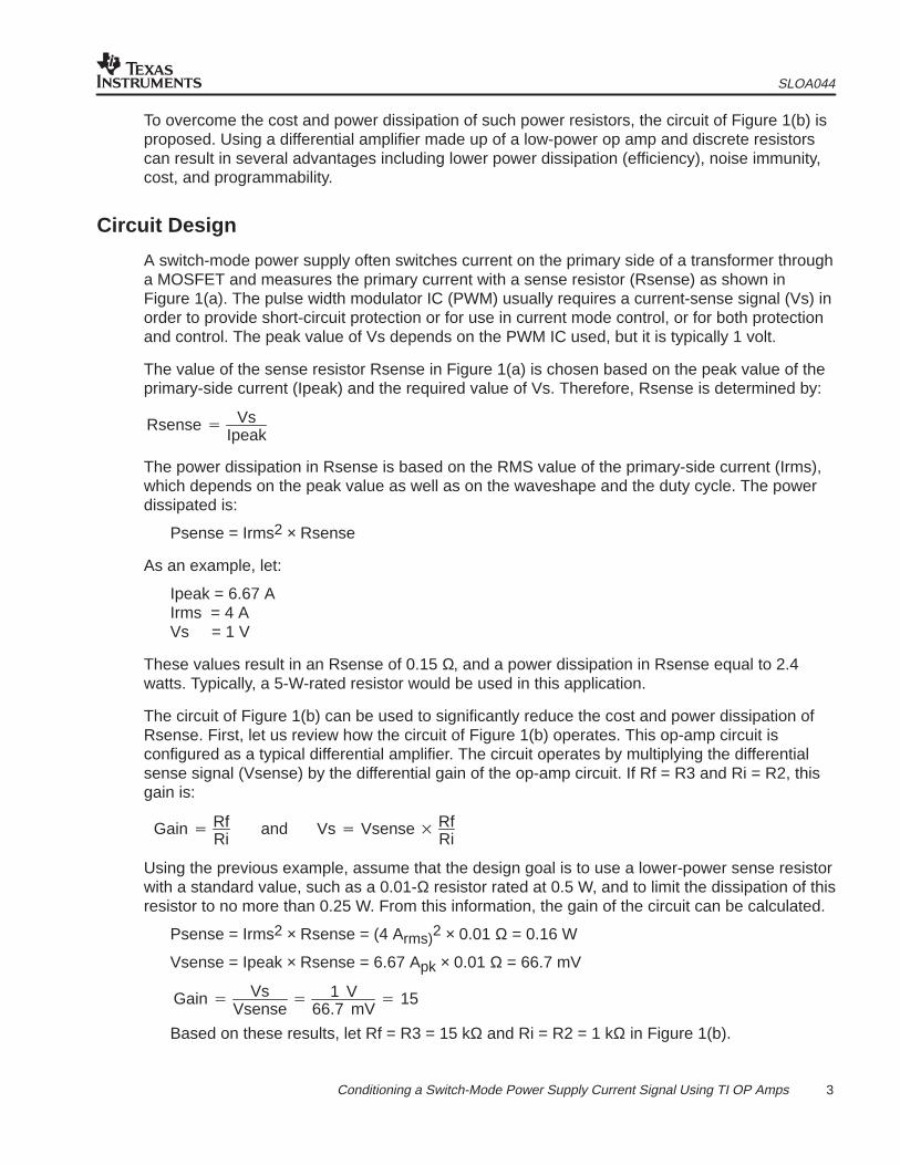
Slew rate and gain-bandwidth product:
trise tfall
1/fs
VSENSE VS
Figure 2. Current Sense Waveforms
Figure 2 shows a representation of Vsense, the current-sense signal across the sense resistor,and Vs, the filtered signal desired at the PWM IC. The leading edge of Vsense contains a spikethat is due to parasitic elements in the power supply, including reverse recovery of diodes andcapacitance of the MOSFET. This spike is undesirable and can be filtered out using thefeedback capacitor Cf, as shown in Figure 1(b). The filter time-constant is often set to be three tofour times the rise time of this spike. The filter’s pole must be set low enough to filter the leadingedge spike, but not so low that the current ramp signal is distorted. The filter pole must thereforebe set above the switching frequency (fs) of the switch-mode power supply. This can beexpressed as:
fc 1(2 RfCf)
1
(8 trise)and fc 3 fs
So, for a rise time (tr) of 100 ns and a 100-kHz switching frequency, this corner frequency wouldbe set to 400 kHz. In this case the limiting factor is the time constant.
Because the circuit filters out frequencies above fc, the gain-bandwidth (GBW) product of the opamp used can be easily calculated as:
GBW fcGain fcRfRi
For the earlier example where the gain was set to 15, and with a 400-kHz corner frequency, theGBW for the desired op amp is calculated to be 6 MHz.
SLOA044
7 Conditioning a Switch-Mode Power Supply Current Signal Using TI OP Amps
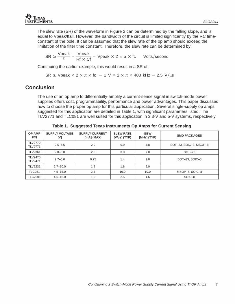
The slew rate (SR) of the waveform in Figure 2 can be determined by the falling slope, and isequal to Vpeak/tfall. However, the bandwidth of the circuit is limited significantly by the RC time-constant of the pole. It can be assumed that the slew rate of the op amp should exceed thelimitation of the filter time constant. Therefore, the slew rate can be determined by:
SRVpeak
VpeakRfCf
Vpeak 2 fc Voltssecond
Continuing the earlier example, this would result in a SR of:
SR Vpeak 2 fc 1 V 2 400 kHz 2.5 Vs
Conclusion
The use of an op amp to differentially-amplify a current-sense signal in switch-mode powersupplies offers cost, programmability, performance and power advantages. This paper discusseshow to choose the proper op amp for this particular application. Several single-supply op ampssuggested for this application are detailed in Table 1, with significant parameters listed. TheTLV2771 and TLC081 are well suited for this application in 3.3-V and 5-V systems, respectively.
Table 1. Suggested Texas Instruments Op Amps for Current Sensing
OP AMPP/N
SUPPLY VOLTAGE[V]
SUPPLY CURRENT[mA] (MAX)
SLEW RATE[V/us] (TYP)
GBW[MHz] (TYP) SMD PACKAGES
TLV2770TLV2771
2.5–5.5 2.0 9.0 4.8 SOT–23, SOIC–8, MSOP–8
TLV2361 2.0–5.0 2.5 3.0 7.0 SOT–23
TLV2470TLV2471
2.7–6.0 0.75 1.4 2.8 SOT–23, SOIC–8
TLV2231 2.7–10.0 1.2 1.6 2.0
TLC081 4.5–16.0 2.5 16.0 10.0 MSOP–8, SOIC–8
TLC2201 4.6–16.0 1.5 2.5 1.6 SOIC–8
IMPORTANT NOTICE
Texas Instruments and its subsidiaries (TI) reserve the right to make changes to their products or to discontinueany product or service without notice, and advise customers to obtain the latest version of relevant informationto verify, before placing orders, that information being relied on is current and complete. All products are soldsubject to the terms and conditions of sale supplied at the time of order acknowledgment, including thosepertaining to warranty, patent infringement, and limitation of liability.
TI warrants performance of its semiconductor products to the specifications applicable at the time of sale inaccordance with TI’s standard warranty. Testing and other quality control techniques are utilized to the extentTI deems necessary to support this warranty. Specific testing of all parameters of each device is not necessarilyperformed, except those mandated by government requirements.
Of course, customers are responsible for their applications using TI components.
In order to minimize risks associated with the customer’s applications, adequate design and operatingsafeguards must be provided by the customer to minimize inherent or procedural hazards.
TI assumes no liability for applications assistance or customer product design. TI does not warrant or representthat any license, either express or implied, is granted under any patent right, copyright, mask work right, or otherintellectual property right of TI covering or relating to any combination, machine, or process in which suchsemiconductor products or services might be or are used. TI’s publication of information regarding any thirdparty’s products or services does not constitute TI’s approval, warranty or endorsement thereof.
Copyright 2000, Texas Instruments Incorporated


![[OPAMP] Analog Devices - Practical Design Techniques for Sensor Signal Conditioning](https://img.pdfslide.net/doc/110x75/552701bf550346f0358b4610/opamp-analog-devices-practical-design-techniques-for-sensor-signal-conditioning.jpg)