Embed Size (px)
Citation preview
C
Simpo PD
Only
F Password Remover Unregistered Version - http://www.simpopdf.com
onfid
entia
l for
truly
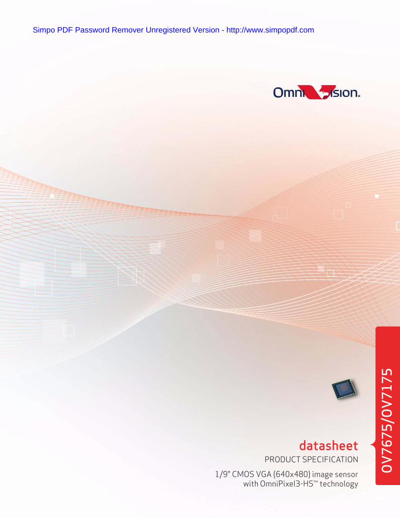
datasheetPRODUCT SPECIFICATION
1/9" CMOS VGA (640x480) image sensorwith OmniPixel3-HS™ technology
OV
7675
/OV
7175

C
Simpo PD
Only
F Password Remover Unregistered Version - http://www.simpopdf.com
onfid
entia
l for
truly
i
Simpo PDF Password Remover Unregistered Version - http://www.simpopdf.com
Con
fiden
tial for
truly Only
00Copyright © 2009 OmniVision Technologies, Inc. All rights reserved.
This document is provided “as is” with no warranties whatsoever, including any warranty of merchantability, non-infringement, fitness for any particular purpose, or any warranty otherwise arising out of any proposal, specification, or sample.
OmniVision Technologies, Inc. and all its affiliates disclaim all liability, including liability for infringement of any proprietary rights, relating to the use of information in this document. No license, expressed or implied, by estoppel or otherwise, to any intellectual property rights is granted herein.
The information contained in this document is considered proprietary to OmniVision Technologies, Inc. and all its affiliates. This information may be distributed to individuals or organizations authorized by OmniVision Technologies, Inc. to receive said information. Individuals and/or organizations are not allowed to re-distribute said information.
Trademark InformationOmniVision and the OmniVision logo are registered trademarks of OmniVision Technologies, Inc. OmniPixel3-HS and VarioPixel are
trademarks of OmniVision Technologies, Inc.
All other trademarks used herein are the property of their respective owners.
To learn more about OmniVision Technologies, visit www.ovt.com.OmniVision Technologies is publicly traded on NASDAQ under the symbol OVTI.
CMOS VGA (640 x 480) image sensor with OmniPixel3-HS™ technology
datasheet (CSP3)PRODUCT SPECIFICATION
version 2.0october 2009
10.13.2009 PRODUCT SPECIFICATION proprietary to OmniVision Technologies
CMOS VGA (640 x 480) image sensor with OmniPixel3-HS™ technologyOV7675/OV7175
Simpo PDF Password Remover Unregistered Version - http://www.simpopdf.com
Con
fiden
tial for
truly Only
proprietary to OmniVision Technologies PRODUCT SPECIFICATION version 2.0

ly
iii
Simpo PDF Password Remover Unregistered Version - http://www.simpopdf.com
ordering informationOV07675-A23A (color, lead-free) 23-pin CSP3
OV07175-A23A (b&w, lead-free) 23-pin CSP3
00applicationscellular phones
toys
PC multimedia
digital still cameras
nl for
truly O00features
support for image sizes: VGA (640x480), QVGA (320x240) and QQVGA (160x120)
support for output formats: YUV4:2:2, Raw RGB, ITU656, RGB565
digital video port (DVP) parallel output interface
on-chip phase lock loop (PLL)
built-in 1.5V regulator for core
capable of maintaining register values at power down
programmable controls for frame rate, mirror and flip, AEC/AGC, and windowing
support for horizontal and vertical sub-sampling
automatic image control functions: automatic exposure control (AEC), automatic white balance (AWB) and automatic black level calibration (ABLC)
image quality controls: defect pixel correction and lens shading correction
support for black sun cancellation
standard serial SCCB interface
parallel I/O tri-state configurability and programmable polarity
module size: 6 mm x 6 mm
Con
fiden
tia00key specificationsactive array size: 640x480
power supply: analog: 2.6 ~ 3.0Vcore: 1.5V DC + 5% (internal regulator)I/O: 1.71 ~ 3.0V
power requirements: active: 98 mWstandby: 60 µW
temperature range: operating: -30°C to 70°C (see table 8-2)stable image: 0°C to 50°C (see table 8-2)
output formats: YUV422, Raw RGB, ITU656, RGB565
lens size: 1/9"
lens chief ray angle: 21° (see figure 10-2)
input clock frequency: 1.5 ~ 27 MHz (see table 8-5)
scan mode: progressive
maximum image transfer rate: (see table 2-1 for details)
sensitivity: 1800 mV/(Lux-sec)
shutter: rolling shutter
S/N ratio: 38 dB
dynamic range: 71 dB
maximum exposure interval: 510 x tROW
pixel size: 2.5 µm x 2.5 µm
dark current: 10 mV/sec @ 60°C
well capacity: 12 Ke-
fixed pattern noise (FPN): 1% of VPEAK-TO-PEAK
image area: 1640 µm x 1220 µm
package dimensions: 2815 x 2825 µm
10.13.2009 PRODUCT SPECIFICATION proprietary to OmniVision Technologies

C
CMOS VGA (640 x 480) image sensor with OmniPixel3-HS™ technologyOV7675/OV7175
Simpo PDF Password Remover Unregistered Version - http://www.simpopdf.com
ly
l for
truly On
onfid
entia
proprietary to OmniVision Technologies PRODUCT SPECIFICATION version 2.0

v
Simpo PDF Password Remover Unregistered Version - http://www.simpopdf.com
Con
fiden
tial for
truly Only
00table of contents
1 signal descriptions 1-1
2 system level description 2-1
2.1 format and frame rate 2-3
2.2 power up sequence 2-3
2.2.1 power up with internal DVDD 2-3
2.3 power management 2-4
2.4 power ON reset generation 2-4
2.5 DOVDD power requirements 2-4
2.6 system clock control 2-4
3 block level description 3-1
3.1 pixel array structure 3-1
4 image sensor core digital functions 4-1
4.1 mirror and flip 4-1
4.2 image windowing 4-2
4.3 test pattern 4-3
4.4 AEC/AGC algorithms 4-4
4.4.1 exposure control 4-4
4.4.2 exposure time 4-4
4.4.3 banding filter 4-4
4.4.4 manual exposure control 4-6
4.4.5 automatic exposure control (AEC) 4-6
4.4.6 average based AEC/AGC 4-7
4.4.7 gain control 4-8
4.4.8 automatic gain control (AGC) 4-8
5 image sensor processor digital functions 5-1
5.1 white balance control 5-1
5.2 automatic white balance 5-1
5.3 manual white balance 5-2
5.4 gamma control 5-2
5.5 gamma slope calculation 5-3
5.6 color matrix 5-4
5.6.1 RGB to YUV conversion matrix 5-5
5.7 lens correction (LENC) 5-5
10.13.2009 PRODUCT SPECIFICATION proprietary to OmniVision Technologies

CMOS VGA (640 x 480) image sensor with OmniPixel3-HS™ technologyOV7675/OV7175
Simpo PDF Password Remover Unregistered Version - http://www.simpopdf.com
Con
fiden
tial for
truly Only
6 image sensor output interface digital functions 6-1
6.1 digital video port (DVP) 6-1
6.1.1 overview 6-1
6.1.2 VGA timing 6-1
7 register tables 7-1
8 operating specifications 8-1
8.1 absolute maximum ratings 8-1
8.2 functional temperature 8-1
8.3 DC characteristics 8-2
8.4 AC characteristics 8-3
9 mechanical specifications 9-1
9.1 physical specifications 9-1
9.2 IR reflow specifications 9-2
10 optical specifications 10-1
10.1 sensor array center 10-1
10.2 lens chief ray angle (CRA) 10-2
proprietary to OmniVision Technologies PRODUCT SPECIFICATION version 2.0

vii
Simpo PDF Password Remover Unregistered Version - http://www.simpopdf.com
Con
fiden
tial for
truly Only
00list of figures
figure 1-1 pin diagram 1-2
figure 2-1 OV7675/OV7175 block diagram 2-1
figure 2-2 reference design schematic (CSP3) 2-2
figure 2-3 power up timing with internal DVDD 2-3
figure 3-1 sensor array region color filter layout 3-1
figure 4-1 mirror and flip samples 4-1
figure 4-2 image windowing 4-2
figure 4-3 test pattern 4-3
figure 4-4 average based AEC/AGC 4-7
figure 5-1 gamma curve 5-2
figure 5-2 lens correction function 5-6
figure 6-1 VGA timing diagram 6-1
figure 6-2 QVGA timing diagram 6-1
figure 6-3 QQVGA timing diagram 6-2
figure 9-1 package specifications 9-1
figure 9-2 IR reflow ramp rate requirements 9-2
figure 10-1 sensor array center 10-1
figure 10-2 chief ray angle (CRA) 10-2
10.13.2009 PRODUCT SPECIFICATION proprietary to OmniVision Technologies

CMOS VGA (640 x 480) image sensor with OmniPixel3-HS™ technologyOV7675/OV7175
Simpo PDF Password Remover Unregistered Version - http://www.simpopdf.com
Con
fiden
tial for
truly Only
proprietary to OmniVision Technologies PRODUCT SPECIFICATION version 2.0

ix
Simpo PDF Password Remover Unregistered Version - http://www.simpopdf.com
Con
fiden
tial for
truly Only
00list of tables
table 1-1 signal descriptions 1-1
table 2-1 format and frame rate 2-3
table 2-2 DOVDD power requirements 2-4
table 4-1 image windowing control functions 4-1
table 4-2 image windowing control functions 4-2
table 4-3 test pattern selection control 4-3
table 4-4 exposure time registers 4-5
table 4-5 exposure control mode registers 4-6
table 4-6 average based AEC/AGC registers 4-7
table 4-7 AGC general control registers 4-8
table 5-1 white balance control registers 5-1
table 5-2 related registers and parameters registers 5-3
table 5-3 color matrix related register and parameter 5-4
table 5-4 LENC related registers 5-5
table 7-1 system control registers 7-1
table 8-1 absolute maximum ratings 8-1
table 8-2 functional temperature 8-1
table 8-3 DC characteristics (-30°C < TA < 70°C) 8-2
table 8-4 AC characteristics (TA = 25°C, VDD-A = 2.8V, VDD-IO = 2.8V) 8-3
table 8-5 timing characteristics 8-3
table 9-1 package dimensions 9-1
table 9-2 reflow conditions 9-2
table 10-1 CRA versus image height plot 10-2
10.13.2009 PRODUCT SPECIFICATION proprietary to OmniVision Technologies

CMOS VGA (640 x 480) image sensor with OmniPixel3-HS™ technologyOV7675/OV7175
Simpo PDF Password Remover Unregistered Version - http://www.simpopdf.com
Con
fiden
tial for
truly Only
proprietary to OmniVision Technologies PRODUCT SPECIFICATION version 2.0

1-1
Simpo PDF Password Remover Unregistered Version - http://www.simpopdf.com
Con
fiden
tial for
truly Only
1 signal descriptionstable 1-1 lists the signal descriptions and their corresponding pin numbers for the OV7675/OV7175 image sensor. The package information is shown in section 9.
table 1-1 signal descriptions
pin number
signal name
pin type
description
A1 SCL input SCCB clock input
A2 SDA I/O SCCB data
A3 AGND ground analog ground
A4 VREF1 reference internal reference: through a 0.1µF capacitor to analog ground
A5 D0 I/O bit[0] of parallel output port / input (LSB)
B1 NC – no connect
B2 AVDD power analog power (2.6 ~ 3.0V)
B3 PWDN input power down, active high (hardware standby when PWDN is high)
B4 D2 I/O bit[2] of parallel output port / input
B5 D1 I/O bit[1] of parallel output port / input
C3 VREF2 reference internal reference: through a 0.1µF capacitor to analog ground
C4 XVCLK input system clock input
C5 D3 I/O bit[3] of parallel output port / input
D1 NC – no connect
D2 PCLK I/O pixel clock output / input
D3 D6 I/O bit[6] of parallel output port / input
D4 D4 I/O bit[4] of parallel output port / input
D5 DGND ground digital core logic and I/O ground
E1 HREF I/O horizontal reference (data valid) output
E2 VSYNC I/O vertical synchronization (VSYNC)
E3 D7 I/O bit[7] of parallel output port / input (MSB)
E4 D5 I/O bit[5] of parallel output port / input
E5 DOVDD power power of I/O circuit (1.7 ~ 3.0V)
10.13.2009 PRODUCT SPECIFICATION proprietary to OmniVision Technologies

CMOS VGA (640 x 480) image sensor with OmniPixel3-HS™ technologyOV7675/OV7175
Simpo PDF Password Remover Unregistered Version - http://www.simpopdf.com
Con
fiden
tial for
truly Only
figure 1-1 pin diagram
OV7675/ OV7175
A1
SCL
A2
SDA
A3
AGND
A4
VREF1
A5
D0
B1
NC
B2
AVDD
B3
PWDN
B4
D2
B5
D1
C3
VREF2
C4
XVCLK
C5
D3
D1
NC
D2
PCLK
D3
D6
D4
D4
D5
DGND
E1
HREF
E2
VSYNC
E3
D7
E4
D5
E5
DOVDD
7675_CSP_DS_1_1
proprietary to OmniVision Technologies PRODUCT SPECIFICATION version 2.0
2-1
Simpo PDF Password Remover Unregistered Version - http://www.simpopdf.com
Con
fiden
tial for
truly Only
2 system level description
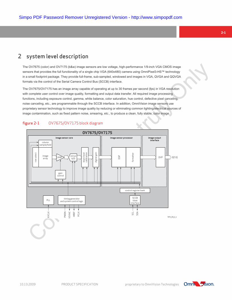
The OV7675 (color) and OV7175 (b&w) image sensors are low voltage, high-performance 1/9-inch VGA CMOS image sensors that provides the full functionality of a single chip VGA (640x480) camera using OmniPixel3-HS™ technology in a small footprint package. They provide full-frame, sub-sampled, windowed and images in VGA, QVGA and QQVGA formats via the control of the Serial Camera Control Bus (SCCB) interface.
The OV7675/OV7175 has an image array capable of operating at up to 30 frames per second (fps) in VGA resolution with complete user control over image quality, formatting and output data transfer. All required image processing functions, including exposure control, gamma, white balance, color saturation, hue control, defective pixel canceling, noise canceling, etc., are programmable through the SCCB interface. In addition, OmniVision image sensors use proprietary sensor technology to improve image quality by reducing or eliminating common lighting/electrical sources of image contamination, such as fixed pattern noise, smearing, etc., to produce a clean, fully stable, color image.
figure 2-1 OV7675/OV7175 block diagram
columnsample/hold
image sensor core
OV7675/OV7175image sensor processor image output
interface
row
sel
ect
blac
k le
vel
calib
rati
on
digi
tal g
ain
PLL
control register bank
SCCBslave
interface
timing generatorand system control logic
DSPimage
array
gaincontrol
XV
CLK
PWD
N
VSY
NC
HR
EF
PCLK
SCL
SDA
AMP 10-bitA/D D[7:0]DVP
7675_DS_2_1
form
atte
r
10.13.2009 PRODUCT SPECIFICATION proprietary to OmniVision Technologies

CMOS VGA (640 x 480) image sensor with OmniPixel3-HS™ technologyOV7675/OV7175
Simpo PDF Password Remover Unregistered Version - http://www.simpopdf.com
Con
fiden
tial for
truly Only
figure 2-2 reference design schematic (CSP3)
U1
OV7675/ OV7175
CSP3
D7 D7E3
D6 D6D3
D5 D5E4
D4 D4D4
D3 D3C5
D2 D2B4
D1 D1B5
D0 D0A5
NC
B1
AVDDB2
VREF1VREF1 A4
VREF2VREF2 C3
AGNDA3
DOVDDE5
DGNDD5
PWDNPWDN B3
PCLK
PCLK
D2
HR
EFH
REF
E1
VSY
NC
VSY
NC
E2
XV
CLK
XV
CLK
C4
SIO
CSC
LA
1
SIO
DSD
AA
2
NC
D1
VREF1T1
VREF2T2
AGNDT3
DGNDT4
VSYNCT5
HREFT6
PCLKT7
DG
ND
AG
ND
DOVDD
V33
AVDD
C8
0.1μ
F-06
03
C7
0.1μ
F-06
03
C6
0.1μ
F-06
03
C5
0.1μ
F-06
03
AG
ND
DG
ND
J2CO
N32
A
D0D2 2
D2D4 4
D4D6 6
D3D1 1
D5D3 3
D7D5 5
D6D8 8D9D7 7
PWDN1PWDN 10RESET9
SIODSIOD 12NC11
SIOCSIOC 14HREFHREF 13
GND 16VSYNCVSYNC 15
GND 18PCLKPCLK 17
XVCLKXCLK 20PWR19
GND 22PWR21
D0 24D123
NC 26NC25
NC 28NC27
NC 30NC29
GND 32GND31
C13
10μF
/16V
+
R1 10-0603 PWDN3DGND
1
2DOVDD
J1A
GN
D
AG
ND
OUT 3VIN2
GND1
U2XC6203E2802P-SOT89
2.8V
C1
1μF-
0603
AVDD 2.8V
C2
10μF
/6V
-EIA
-A
V33
C4
10μF
/6V
-EIA
-A
L1 3.3μH-L1008
C3
0.1μ
F-06
03
DG
ND
DG
ND
OUT 3VIN2
GND1
U3XC62FP1802-SOT89
1.8V
C9
1μF-
0603
DOVDD 1.8V
C10
10μF
/6V
-EIA
-A
V33
C12
10μF
/6V
-EIA
-A
L2 3.3μH-L1008
C11
0.1μ
F-06
03
7675_CSP_DS_2_2
proprietary to OmniVision Technologies PRODUCT SPECIFICATION version 2.0

2-3
Simpo PDF Password Remover Unregistered Version - http://www.simpopdf.com
Con
fiden
tial for
truly Only
2.1 format and frame rate
The OV7675/OV7175 supports the following formats YUV422, RAW RGB, ITU656, and RGB565.
2.2 power up sequence
2.2.1 power up with internal DVDD
When powering up with the internal DVDD and SCCB access during the power ON period, the following conditions must occur:
1. if VDD-IO and VDD-A are turned ON at the same time, make sure VDD-IO becomes stable before VDD-A becomes stable
2. PWDN is active high with an asynchronized design (does not need clock)3. PWDN must go high during the power up period4. for PWDN to go low, power up must first become stable (AVDD to PWDN > 5 ms)5. master clock XVCLK should provide at least 1 ms before host accesses sensor’s I2C6. host can access I2C bus (if shared) during entire period. 20 ms after PWDN goes low goes high if reset is
inserted after PWDN goes low, host can access sensor’s SCCB to initialize sensor
figure 2-3 power up timing with internal DVDD
table 2-1 format and frame rate
format resolution frame rate scaling method pixel clock (YUV/RAW)
VGA 640x480 30 fps full 24/12 MHz
QVGA 320x240 60 fps sub sampling from VGA 24/12 MHz
QQVGA 160x120 240 fps cropped and window from center of VGA 24/12 MHz
VDD_IO(DOVDD)
VDD_A(AVDD)
SCCB activity is okay during entire period
power down
VDD_IO first, then VDD_A, and rising time is less than 5 ms
PWDN
SCCB
note T0 ≥ 0 ms: delay from VDD_IO stable to VDD_A stableT2 ≥ 5 ms: delay from VDD_A stable to sensor power up stableif PWDN is not used, sensor SCCB is accessible after TO + T2
T0
T2
power on period
7675_DS_2_3
10.13.2009 PRODUCT SPECIFICATION proprietary to OmniVision Technologies
CMOS VGA (640 x 480) image sensor with OmniPixel3-HS™ technologyOV7675/OV7175
Simpo PDF Password Remover Unregistered Version - http://www.simpopdf.com
Con
fiden
tial for
truly Only
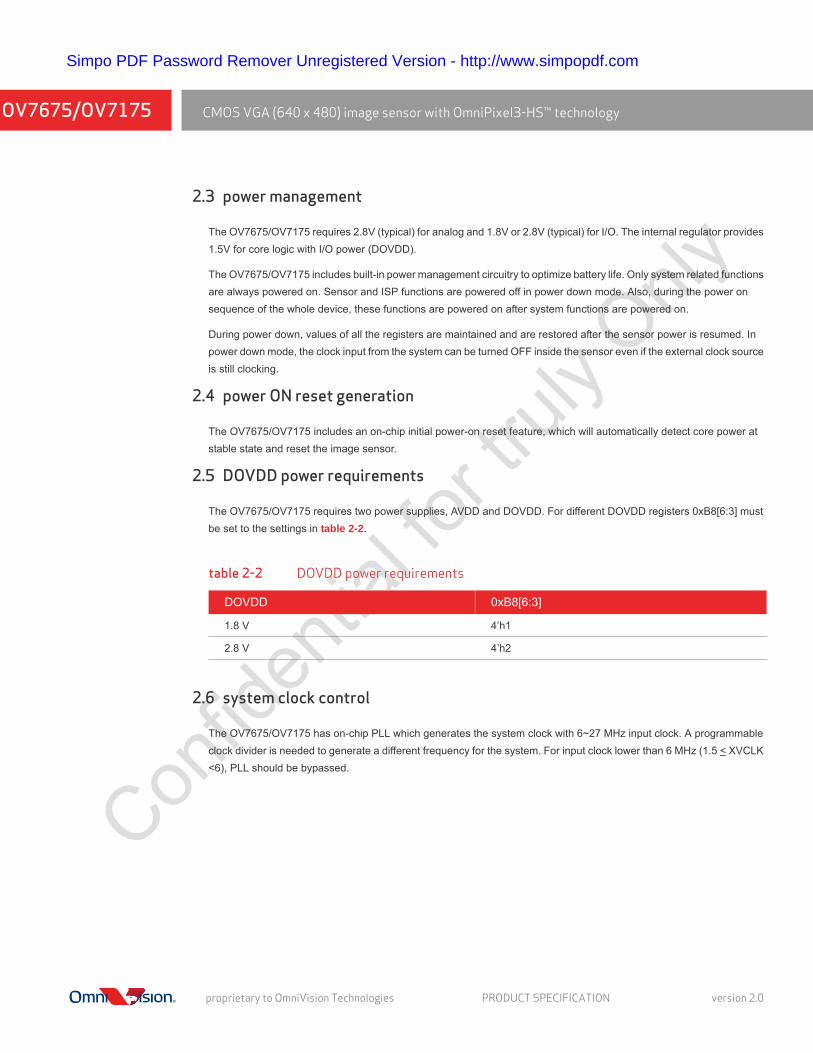
2.3 power management
The OV7675/OV7175 requires 2.8V (typical) for analog and 1.8V or 2.8V (typical) for I/O. The internal regulator provides 1.5V for core logic with I/O power (DOVDD).
The OV7675/OV7175 includes built-in power management circuitry to optimize battery life. Only system related functions are always powered on. Sensor and ISP functions are powered off in power down mode. Also, during the power on sequence of the whole device, these functions are powered on after system functions are powered on.
During power down, values of all the registers are maintained and are restored after the sensor power is resumed. In power down mode, the clock input from the system can be turned OFF inside the sensor even if the external clock source is still clocking.
2.4 power ON reset generation
The OV7675/OV7175 includes an on-chip initial power-on reset feature, which will automatically detect core power at stable state and reset the image sensor.
2.5 DOVDD power requirements
The OV7675/OV7175 requires two power supplies, AVDD and DOVDD. For different DOVDD registers 0xB8[6:3] must be set to the settings in table 2-2.
2.6 system clock control
The OV7675/OV7175 has on-chip PLL which generates the system clock with 6~27 MHz input clock. A programmable clock divider is needed to generate a different frequency for the system. For input clock lower than 6 MHz (1.5 < XVCLK <6), PLL should be bypassed.
table 2-2 DOVDD power requirements
DOVDD 0xB8[6:3]
1.8 V 4’h1
2.8 V 4’h2
proprietary to OmniVision Technologies PRODUCT SPECIFICATION version 2.0

3-1
Simpo PDF Password Remover Unregistered Version - http://www.simpopdf.com
Con
fiden
tial for
truly Only
3 block level description
3.1 pixel array structure
The OV7675/OV7175 sensor has an image array of 656 columns by 504 rows (330,624 pixels). figure 3-1 shows a cross-section of the image sensor array.
The color filters are arranged in a Bayer pattern. The primary color BG/GR array is arranged in line-alternating fashion. Of the 330,624 pixels, 322,752 (656x492) are active pixels and can be output.
The sensor array design is based on a field integration read-out system with line-by-line transfer and an electronic shutter with a synchronous pixel read-out scheme.
figure 3-1 sensor array region color filter layout
B GbGr R
B GbGr R
B GbGr R
B GbGr R
B GbGr R
B GbGr R
B GbGr R
B GbGr R
B GbGr R
B GbGr R
B GbGr R
B GbGr R
B GbGr R
B GbGr R
B GbGr R
B GbGr R
B GbGr R
B GbGr R
B GbGr R
B GbGr R
B GbGr R
B GbGr R
B GbGr R
B GbGr R
B GbGr R
B GbGr R
B GbGr R
B GbGr R
B GbGr R
B GbGr R
B GbGr R
B GbGr R
B GbGr R
B GbGr R
B GbGr R
B GbGr R
B GbGr R
B GbGr R
B GbGr R
B GbGr R
B GbGr R
B GbGr R
B GbGr R
B GbGr R
B GbGr R
B GbGr R
B GbGr R
B GbGr R
0 1 2 3 4 5 650
651
652
653
654
655
1415
500501502503
row
s
columns
dummydummydummydummy
dummydummydummydummy
13121110
98
3210
B GbGr R
B GbGr R
B GbGr R
B GbGr R
B GbGr R
B GbGr R
B GbGr R
B GbGr R
B GbGr R
B GbGr R
B GbGr R
B GbGr R
dummydummy
7654
dum
my
dum
my
dum
my
dum
my
dum
my
dum
my
dum
my
dum
my
dum
my
dum
my
dum
my
dum
my
dum
my
dum
my
dum
my
dum
my
B GbGr R
B GbGr R
B GbGr R
B GbGr R
B GbGr R
B GbGr R
B GbGr R
B GbGr R
B GbGr R
B GbGr R
B GbGr R
B GbGr R
B GbGr R
B GbGr R
B GbGr R
B GbGr R
B GbGr R
B GbGr R
B GbGr R
B GbGr R
B GbGr R
B GbGr R
B GbGr R
B GbGr R
B GbGr R
B GbGr R
B GbGr R
6 7 8 9 10 11
B GbGr R
B GbGr R
B GbGr R
B GbGr R
B GbGr R
B GbGr R
B GbGr R
B GbGr R
B GbGr R
B GbGr R
B GbGr R
B GbGr R
B GbGr R
B GbGr R
B GbGr R
B GbGr R
B GbGr R
B GbGr R
B GbGr R
B GbGr R
B GbGr R
B GbGr R
B GbGr R
B GbGr R
B GbGr R
B GbGr R
B GbGr R
B GbGr R
B GbGr R
B GbGr R
B GbGr R
B GbGr R
B GbGr R
B GbGr R
B GbGr R
B GbGr R
644
645
646
647
648
649
B GbGr R
B GbGr R
B GbGr R
B GbGr R
B GbGr R
B GbGr R
B GbGr R
B GbGr R
B GbGr R
498499
dummydummydummy
activepixel
activepixel
7675_DS_3_1
10.13.2009 PRODUCT SPECIFICATION proprietary to OmniVision Technologies

CMOS VGA (640 x 480) image sensor with OmniPixel3-HS™ technologyOV7675/OV7175
Simpo PDF Password Remover Unregistered Version - http://www.simpopdf.com
Con
fiden
tial for
truly Only
proprietary to OmniVision Technologies PRODUCT SPECIFICATION version 2.0

4-1
Simpo PDF Password Remover Unregistered Version - http://www.simpopdf.com
Con
fiden
tial for
truly Only
4 image sensor core digital functions
4.1 mirror and flip
The OV7675/OV7175 provides Mirror and Flip read-out modes, which respectively reverse the sensor data read-out order horizontally and vertically (see figure 4-1).
figure 4-1 mirror and flip samples
table 4-1 image windowing control functions
address
register name
default value
R/W
description
0x1E MVFP 0x01 RW
Mirror/VFlip EnableBit[5]: Mirror
0: Normal image1: Mirror image
Bit[4]: VFlip enable0: Normal image1: Vertically flip image
Foriginal image
F
flipped image
Fmirrored image
F
mirrored and flippedimage
7675_DS_4_1
10.13.2009 PRODUCT SPECIFICATION proprietary to OmniVision Technologies

CMOS VGA (640 x 480) image sensor with OmniPixel3-HS™ technologyOV7675/OV7175
Simpo PDF Password Remover Unregistered Version - http://www.simpopdf.com
Con
fiden
tial for
truly Only
4.2 image windowing
The OV7675/OV7175 windowing feature allows the users to define the active pixels used in the final image (frame) as required for low-resolution applications. Selecting the Start/Stop Row/Column addresses (modifying window size and/or position) does not change the frame or data rate. When windowing is enabled, the HREF signal is asserted to be consistent with the programmed 'active' horizontal and vertical region.
figure 4-2 image windowing
table 4-2 image windowing control functions
register address description
0x17[7:0], 0x32[2:0] horizontal frame (HREF column) start
0x18[7:0], 0x32[5:3] horizontal frame (HREF column) stop
0x19[7:0], 0x03[2:0] vertical frame (row) start
0x1A[7:0], 0x03[5:3] vertical frame (row) stop
framewindowingzoom area
image sensing area
vert
ical
fram
e en
d{0
x1A
[7:0
], 0x
03[5
:3]}
++
vert
ical
fram
e st
art
{0x1
9[7:
0], 0
x03[
2:0]
}
480
lines
VR
EF(w
indo
win
g m
ode)
VR
EF(f
ull r
esol
utio
n)
VSY
NC
horizontal frame end{0x18[7:0], 0x32[5:3]}
+ +
horizontal frame start{0x17[7:0], 0x32[2:0]}
492
row
s656 columns
640 pixels
HREF(windowing mode)
HREF(full resolution)
HSYNC
7675_DS_4_2
proprietary to OmniVision Technologies PRODUCT SPECIFICATION version 2.0

4-3
Simpo PDF Password Remover Unregistered Version - http://www.simpopdf.com
Con
fiden
tial for
truly Only
4.3 test pattern
For testing purposes, the OV7675 offers one type of test pattern, color bar.
figure 4-3 test pattern
table 4-3 test pattern selection controla
a. only for VGA
address
register name
default value
R/W
description
0x71 COM17 0x00 RWBit[7]: Color bar enable
0: Disabled1: Enabled
color bar
10.13.2009 PRODUCT SPECIFICATION proprietary to OmniVision Technologies

CMOS VGA (640 x 480) image sensor with OmniPixel3-HS™ technologyOV7675/OV7175
Simpo PDF Password Remover Unregistered Version - http://www.simpopdf.com
Con
fiden
tial for
truly Only
4.4 AEC/AGC algorithms
4.4.1 exposure control
The OV7675/OV7175 supports both automatic and manual exposure control modes. The exposure time is defined as the interval from the cell pre-charge to the end of the photo-induced current measurement and can be controlled manually or by using the AEC function. This exposure control uses a ’rolling’ shutter, which means the exposure time is set on a row-by-row basis rather than on a frame-by-frame basis.
4.4.2 exposure time
Exposure time unit is the interval of row, as shown below.
tExposure = AEC[15:0] x tRow interval
where AEC[15:0] is set by register {0x07[5:0], 0x10[7:0], 0x04[1:0]}
AEC[15:0] = {0x07[5:0], 0x10[7:0], 0x04[1:0]}
The OV7675 array always output, VGA resolution, the row interval is
tRow interval = 2 x (784 + Dummy Pixels) x tINT CLK,
and AEC[15:0] is limited by the number of rows of VGA resolution plus the number of dummy lines.
Note that both the AEC and AGC functions are interactive so registers and functions may be common to both. Also, in general, the AEC is the primary control and will be adjusted before the AGC (AGC acts to adjust and center the AEC).
The algorithm used for the electronic exposure control is based on luminance of the full, center quarter, or center half image. The exposure is optimized for a “normal” scene that assumes the subject is well lit relative to the background.
4.4.3 banding filter
The OV7675/OV7175 also provides a rolling horizontal band eliminate function in auto exposure mode. A banding filter is deployed to filter out the banding effect caused by the 50/60 Hz lighting. To enable this function, register 0x13[5] must be set to high. The OV7675/OV7175 only supports manual banding filter.
In 50 or 60Hz flicker light, the exposure time must be a multiple of the flicker interval to avoid band shown on the image. For 50Hz light, the exposure time must be
tExposure = N/100
and for 60Hz light, the exposure time must be
tExposure = N/120
where N is a positive integer.
proprietary to OmniVision Technologies PRODUCT SPECIFICATION version 2.0

4-5
Simpo PDF Password Remover Unregistered Version - http://www.simpopdf.com
Con
fiden
tial for
truly Only
Since the exposure time AEC[15:0] is based on row interval, the AEC needs to know 1/100 second and 1/120 second is equal to how many rows. Banding filter registers, BD50st and BD60st, are used to set 1/100 and 1/120 second. The banding filter can be calculated by:
where maximum exposure equals to the number of lines per frame plus the number of dummy lines minus 2.
The OV7675/OV7175 can also disable the banding filter to allow for any exposure time value. When banding filter is enabled, the OV7675/OV7175 also allows the exposure time to be less than 1/120 or 1/100 second under strong light condition, by setting register 0x13[4] to 1.
table 4-4 summarizes the registers of exposure time and how to set the banding filter.
table 4-4 exposure time registers (sheet 1 of 2)
address register name description
0x04 COM1 Bit[1:0]: Exposure time, the unit is tRow intervalAEC[15:0] = {0x07[5:0], 0x10[7:0], 0x04[1:0]}
0x10 AEC Bit[7:0]: Exposure time, the unit is tRow intervalAEC[15:0] = {0x07[5:0], 0x10[7:0], 0x04[1:0]}
0x07 AECHH Bit[5:0]: Exposure time, the unit is tRow intervalAEC[15:0] = {0x07[5:0], 0x10[7:0], 0x04[1:0]}
0x13 COM8
Bit[5]: Banding filter enable/disable0: Disable banding filter, the exposure time can be any number1: Enable banding filter, the exposure time must be N/100 or
N/120 second.
0x3B COM11
Bit[3]: Manual banding filter selection (effective only when COM11[4] = 0)0: Select the value of register 0x50 as banding filter (60Hz)1: Select the value of register 0x4F as banding filter (50Hz)
0xE1 REGE1 Bit[1:0]: Banding filter for 50Hz[9:8]Banding filter for 50Hz[9:0] = (0xE1[1:0],0x9D[7:0])
0x9D BD50ST Bit[7:0]: Banding filter for 50Hz[7:0]Banding filter for 50Hz[9:0] = (0xE1[1:0],0x9D[7:0])
0xE1 REGE1 Bit[3:2]: Banding filter for 60Hz[9:8]Banding filter for 60Hz[9:0] = (0xE1[3:2],0x9E[7:0])
0x9E BD60ST Bit[7:0]: Banding filter for 60Hz[7:0]Banding filter for 60Hz[9:0] = (0xE1[3:2],0x9E[7:0])
banding filter value = for 60Hz=120 x tRow interval
1
120
framerate x maximum exposure
banding filter value = for 50Hz=100 x tRow interval
1
100
framerate x maximum exposure
10.13.2009 PRODUCT SPECIFICATION proprietary to OmniVision Technologies
CMOS VGA (640 x 480) image sensor with OmniPixel3-HS™ technologyOV7675/OV7175
Simpo PDF Password Remover Unregistered Version - http://www.simpopdf.com
Con
fiden
tial for
truly Only
4.4.4 manual exposure control
The OV7675/OV7175 works in manual exposure mode when register 0x13[0] is low. In manual exposure control mode the companion backend processor can fully control the OV7675/OV7175 image exposure. The companion backend processor may write exposure values to AEC [15:0] according to its corresponding Automatic Exposure Control (AEC) algorithm.
The companion processor also needs to set correct exposure time to avoid banding in flicker light. Refer to section 3.3.1 and 3.3.2 for the exposure time calculation.
4.4.5 automatic exposure control (AEC)
The AEC function allows for the image sensor to adjust the exposure without external command or control. The OV7675/OV7175 supports average based AEC. Note that both AEC and AGC functions are controlled by the same algorithm and share the same registers of the algorithm parameter. In general, the AEC is the primary control and will be adjusted before the AGC (AGC acts to adjust and center the AEC).
The average based AEC/AGC defines the fast operating region in which the AEC/AGC adjusts the image luminance very fast by increasing the exposure time and gain adjustment.
0xA5 BD50MAX Bit[7:0]: Banding filter maximum step for 50Hz light source
0xAB BD60MAX Bit[7:0]: Banding filter maximum step for 60Hz light source
0x3B COM11
Bit[1]: Exposure time option0: Limit the minimum exposure time to 1/100 or 1/120 second
in any light condition when banding filter is enabled1: Allow exposure time to be less than 1/100 or 1/120 second
under strong light conditions when banding filter is enabled
table 4-5 exposure control mode registers
address register name description
0x13 COM8Bit[7]: AEC operation speed
0: Normal speed1: Fast speed
0x13 COM8Bit[6]: AEC step size limit
0: Unlimited step size1: Step size limited to vertical bank
0x13 COM8Bit[3]: Pixel level exposure ON/OFF selection
0: Limit the minimum exposure time to 1 line1: Allow exposure time less than 1 line
0x13 COM8Bit[0]: AEC enable
0: Disable AEC1: Enable AEC
table 4-4 exposure time registers (sheet 2 of 2)
address register name description
proprietary to OmniVision Technologies PRODUCT SPECIFICATION version 2.0

4-7
Simpo PDF Password Remover Unregistered Version - http://www.simpopdf.com
Con
fiden
tial for
truly Only
4.4.6 average based AEC/AGC
As shown in figure 4-4, the average based AEC/AGC algorithm makes the average value of the luminance converge to the Stable Operating Region step by step. Outside the Control Zone, the AEC/AGC adjusts exposure time and gain by big steps to lower luminance quickly. Inside the Control Zone and outside the Stable Operating range, the AEC/AGC adjusts exposure time and gain by small step to make the luminance level converge to the Stable Operating Region smoothly. Inside Stable Operating Region, the AEC/AGC does not adjust exposure time and gain anymore. table 4-6 summarizes the control registers of the average based AEC/AGC.
figure 4-4 average based AEC/AGC
table 4-6 average based AEC/AGC registers
address register name description
0x24 AEW Bit[7:0]: Upper limit of the Stable Operating Region
0x25 AEB Bit[7:0]: Lower limit of the Stable Operating Region
0x26 VPT Bit[7:4]: High nibble of upper limit of fast mode control zoneThe upper limit is {0x26[7:4], 4’h0}
0x26 VPT Bit[3:0]: High nibble of lower limit of fast mode control zoneThe lower limit is {0x26[3:0], 4’h0}
0x0D COM4
Bit[5:4]: Average option (must be same value as 0x0D[7:6])00: Full window01: 1/2 window1x: 1/4 window
0x42 COM17
Bit[5:4]: Average option (must be same value as 0x42[5:4])00: Full window01: 1/2 window1x: 1/4 window
control zone stable operating region
desired convergence
7675_DS_4_4
10.13.2009 PRODUCT SPECIFICATION proprietary to OmniVision Technologies

CMOS VGA (640 x 480) image sensor with OmniPixel3-HS™ technologyOV7675/OV7175
Simpo PDF Password Remover Unregistered Version - http://www.simpopdf.com
Con
fiden
tial for
truly Only
4.4.7 gain control
The OV7675/OV7175 supports both automatic gain control (AGC) and manual gain control modes.
4.4.7.1 manual gain controlThe manual gain control mode allows for the companion backend processor to control the OV7675/OV7175 gain value. The companion backend chip can write gain values to register {0x03[7:6],0x00[7:0]} according to its gain control algorithm. The formula to calculate gain from register value is:
The gain to register value correlation is shown in table 4-7.
4.4.8 automatic gain control (AGC)
The AGC function allows the image sensor to adjust image luminance by changing gain without external command or control. Register setting 0x13[2] enables or disables AGC function. When AGC function is enabled, gain is automatically adjusted and the result is saved in register 0x00[6:0]. The maximum gain is limited by gain ceiling (refer to table 4-7). When the AGC function is disabled, the gain control is still active, and user can change the gain setting.
The AGC uses the same algorithm as the AEC and shares most of the control registers with the AEC. table 4-7 summarizes the general controls for the AGC. To achieve best image quality, the sensor always increases exposure time prior to gain and reduces gain prior to exposure time.
table 4-7 AGC general control registers
address register name description
0x13 REG13Bit[2]: AGC function auto/manual selection
0: manual gain control1: automatic gain control enable
0x00 GAIN
Bit[7:0]: Gain setting. Read-only when AGC is enabled. When AGC is disabled, these registers can be programmed manually
.
0x03 VREF
Bit[7:6]: Gain setting. Read-only when AGC is enabled. When AGC is disabled, these registers can be programmed manually
.
0x14 REG14
Bit[6:4]: Automatic gain ceiling - maximum AGC value000: 2x001: 4x010: 8x011: 16x100: 32x101 64x110: 128x111: Not used
gain = (0x03[7] + 1) x (0x03[6] + 1) x (0x00[7] + 1) (0x00[6] + 1) x
(0x00[5] + 1) x (0x00[4] + 1) x ( + 1)0x00[3:0]
16
gain = (0x03[7] + 1) x (0x03[6] + 1) x (0x00[7] + 1) (0x00[6] + 1) x
(0x00[5] + 1) x (0x00[4] + 1) x ( + 1)0x00[3:0]
16
gain = (0x03[7] + 1) x (0x03[6] + 1) x (0x00[7] + 1) (0x00[6] + 1) x
(0x00[5] + 1) x (0x00[4] + 1) x ( + 1)0x00[3:0]
16
proprietary to OmniVision Technologies PRODUCT SPECIFICATION version 2.0
5-1
Simpo PDF Password Remover Unregistered Version - http://www.simpopdf.com
Con
fiden
tial for
truly Only
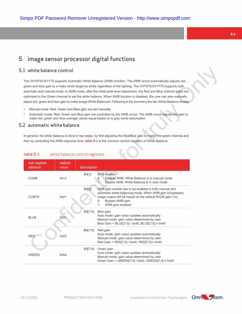
5 image sensor processor digital functions
5.1 white balance control
The OV7675/OV7175 supports Automatic White Balance (AWB) function. The AWB circuit automatically adjusts red, green and blue gain to a make white target be white regardless of the lighting. The OV7675/OV7175 supports both automatic and manual mode. In AWB mode, after the initial pixel level adjustment, the Red and Blue channel gains are optimized to the Green channel to set the white balance. When AWB function is disabled, the user can also manually adjust red, green and blue gain to make image White Balanced. Following is the summery the two White Balance modes.
• Manual mode: Red, Green and Blue gain are set manually• Automatic mode: Red, Green and Blue gain are controlled by the AWB circuit. The AWB circuit adjusts the gain to
make red, green and blue average values equal based on a grey world assumption
5.2 automatic white balance
In general, the white balance is done in two steps: by first adjusting the Red/Blue gain to match the green channel and then by controlling the AWB response time. table 5-1 is the common control registers of White Balance.
table 5-1 white balance control registers
sub register address
default value
description
COM8 0x13Bit[1]: AWB enable
0: Disable AWB, White Balance is in manual mode1: Enable AWB, White Balance is in auto mode
COM16 0x41
Bit[3]: AWB gain enable has to be enabled in both manual and automatic white balancing mode. When AWB gain is bypassed, image output will be based on the default R/G/B gain (1x).0: Bypass AWB gain1: AWB gain enabled
BLUE 0x01
Bit[7:0]: Blue gainAuto mode: gain value updates automaticallyManual mode: gain value determined by user.Blue Gain = BLUE[7:0] / 0x40, BLUE[7:0] ≥ 0x40
RED 0x02
Bit[7:0]: Red gainAuto mode: gain value updates automaticallyManual mode: gain value determined by user.Red Gain = RED[7:0] / 0x40, RED[7:0] ≥ 0x40
GREEN 0x6A
Bit[7:0]: Green gain Auto mode: gain value updates automaticallyManual mode: gain value determined by user.Green Gain = GREEN[7:0] / 0x40, GREEN[7:0] ≥ 0x40
10.13.2009 PRODUCT SPECIFICATION proprietary to OmniVision Technologies

CMOS VGA (640 x 480) image sensor with OmniPixel3-HS™ technologyOV7675/OV7175
Simpo PDF Password Remover Unregistered Version - http://www.simpopdf.com
Con
fiden
tial for
truly Only
5.3 manual white balance
In manual mode, the companion backend processor can control the OV7675/OV7175 internal Red, Green and Blue gain register values to achieve white balance. The gain is calculated by the equation below:
Gain = Register Value / 0x40
Since the gain is digital gain, always set the minimum gain of the three channels to 1x and do not apply less than 1x gain to any channel.
5.4 gamma control
The OV7675 gamma curve is composed of approximately 16 linear segments as shown in figure 5-1 and table 5-1.
figure 5-1 gamma curve
XR
EF1
XR
EF2
XR
EF3
XR
EF15 25
5
GAM1
0
SLOP
GAM2
GAM3
GAM15
255
7675_DS_5_1
proprietary to OmniVision Technologies PRODUCT SPECIFICATION version 2.0

5-3
Simpo PDF Password Remover Unregistered Version - http://www.simpopdf.com
Con
fiden
tial for
truly Only
5.5 gamma slope calculation
The highest segment slope (register SLOP 0x81) is calculated by the following equation:
SLOP[7:0] = (255 - GAM15[7:0]) * 40/30
table 5-2 related registers and parameters registers
gamma segments Y coordinates gamma segments X coordinates
register address name value
DSP_CTL0 0x60[1] gamma function enabled 0: gamma disabled1: gamma enabled
GAM1 0x7B XREF1 4
GAM2 0x7C XREF2 8
GAM3 0x7D XREF3 16
GAM4 0x7E XREF4 32
GAM5 0x7F XREF5 40
GAM6 0x80 XREF6 48
GAM7 0x81 XREF7 56
GAM8 0x82 XREF8 64
GAM9 0x83 XREF9 72
GAM10 0x84 XREF10 80
GAM11 0x85 XREF11 96
GAM12 0x86 XREF12 112
GAM13 0x87 XREF13 144
GAM14 0x88 XREF14 176
GAM15 0x89 XREF15 208
SLOP 0x7A SLOP = (256 – GAM15) * 40/30
10.13.2009 PRODUCT SPECIFICATION proprietary to OmniVision Technologies
CMOS VGA (640 x 480) image sensor with OmniPixel3-HS™ technologyOV7675/OV7175
Simpo PDF Password Remover Unregistered Version - http://www.simpopdf.com
Con
fiden
tial for
truly Only
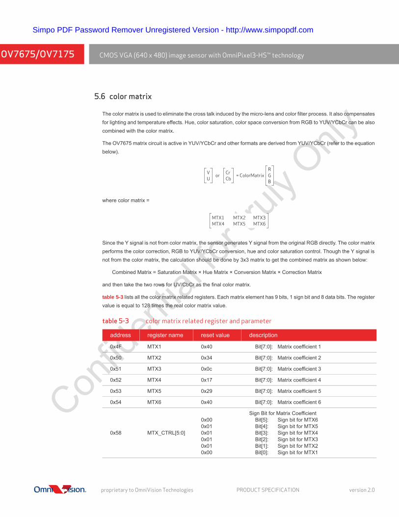
5.6 color matrix
The color matrix is used to eliminate the cross talk induced by the micro-lens and color filter process. It also compensates for lighting and temperature effects. Hue, color saturation, color space conversion from RGB to YUV/YCbCr can be also combined with the color matrix.
The OV7675 matrix circuit is active in YUV/YCbCr and other formats are derived from YUV/YCbCr (refer to the equation below).
where color matrix =
Since the Y signal is not from color matrix, the sensor generates Y signal from the original RGB directly. The color matrix performs the color correction, RGB to YUV/YCbCr conversion, hue and color saturation control. Though the Y signal is not from the color matrix, the calculation should be done by 3x3 matrix to get the combined matrix as shown below:
Combined Matrix = Saturation Matrix × Hue Matrix × Conversion Matrix × Correction Matrix
and then take the two rows for UV/CbCr as the final color matrix.
table 5-3 lists all the color matrix related registers. Each matrix element has 9 bits, 1 sign bit and 8 data bits. The register value is equal to 128 times the real color matrix value.
table 5-3 color matrix related register and parameter
address register name reset value description
0x4F MTX1 0x40 Bit[7:0]: Matrix coefficient 1
0x50 MTX2 0x34 Bit[7:0]: Matrix coefficient 2
0x51 MTX3 0x0c Bit[7:0]: Matrix coefficient 3
0x52 MTX4 0x17 Bit[7:0]: Matrix coefficient 4
0x53 MTX5 0x29 Bit[7:0]: Matrix coefficient 5
0x54 MTX6 0x40 Bit[7:0]: Matrix coefficient 6
0x58 MTX_CTRL[5:0]
0x000x010x010x010x010x00
Sign Bit for Matrix CoefficientBit[5]: Sign bit for MTX6Bit[4]: Sign bit for MTX5Bit[3]: Sign bit for MTX4Bit[2]: Sign bit for MTX3Bit[1]: Sign bit for MTX2Bit[0]: Sign bit for MTX1
or = ColorMatrixVU
RGB
CrCb
MTX1MTX4
MTX2MTX5
MTX3MTX6
proprietary to OmniVision Technologies PRODUCT SPECIFICATION version 2.0

5-5
Simpo PDF Password Remover Unregistered Version - http://www.simpopdf.com
Con
fiden
tial for
truly Only
5.6.1 RGB to YUV conversion matrix
The color conversion matrix can be derived from the standard equations below:
Y = 0.59G + 0.31R + 0.11B
U = B - Y
V = R - Y
Cr = 0.713 (R - Y)
Cb = 0.563 (B - Y)
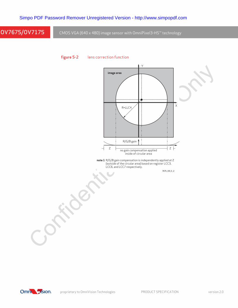
5.7 lens correction (LENC)
The main purpose of the Lens Correction (LENC) function is to compensate for lens imperfection. According to the radius of each pixel to the lens, the module calculates a gain for the pixel, correcting each pixel with its gain calculated to compensate for the light distribution due to lens curvature.
Due to the lens roll off, the pixels in the edge and corner area receive much less light than the pixels in the center area, which makes the image darker in the edges and corner areas. The lens correction function amplifies pixel output based on the distance from the pixel to the lens optical center to achieve uniform image. table 5-4 lists lens correction related registers, and figure 5-2 shows the lens correction function of OV7675/OV7175.
table 5-4 LENC related registers
address register name description
0x55 LCC5
Bit[2]: Lens correction control select0: R, G, and B channel compensation coefficient is set by
0x641: R, G, and B channel compensation coefficient is set by
registers and respectivelyBit[0]: Lens correction enable
0: Disabled1: Enabled
0x62 LCC1
Lens Correction Option 1Bit[7]: Sign bit for X coordinate of lens correction center relative to
array center0: Coordinate is + 0x62[6:0]1: Coordinate is - 0x62[6:0]
0x63 LCC2
Lens Correction Option 2Bit[7]: Sign bit for Y coordinate of lens correction center relative to
array center0: Coordinate is + 0x63[6:0]1: Coordinate is - 0x63[6:0]
0x65 LCC4 Radius of the circle, no compensation will be applied inside the circle
0x64 LCC3 G Channel Compensation Coefficient when LCC5[2] (0x66) is 1R, G, and B Channel Compensation Coefficient when LCC5[2] (0x66) is 0
0x94 LCC6 B channel compensation coefficient (effective only when LCC5[2] is high)
0x95 LCC7 R channel compensation coefficient (effective only when LCC5[2] is high)
10.13.2009 PRODUCT SPECIFICATION proprietary to OmniVision Technologies
CMOS VGA (640 x 480) image sensor with OmniPixel3-HS™ technologyOV7675/OV7175
Simpo PDF Password Remover Unregistered Version - http://www.simpopdf.com
Con
fiden
tial for
truly Only
figure 5-2 lens correction function
R=LLC4X
ZZ
R/G/B gain
note 1 R/G/B gain compensation is independently applied at Z(outside of the circular area) based on register LCC3,LCC6, and LCC7 respectively.
no gain compensation appliedinside of circular area
image area
-Y
7675_DS_5_2
proprietary to OmniVision Technologies PRODUCT SPECIFICATION version 2.0
6-1
Simpo PDF Password Remover Unregistered Version - http://www.simpopdf.com
Con
fiden
tial for
truly Only
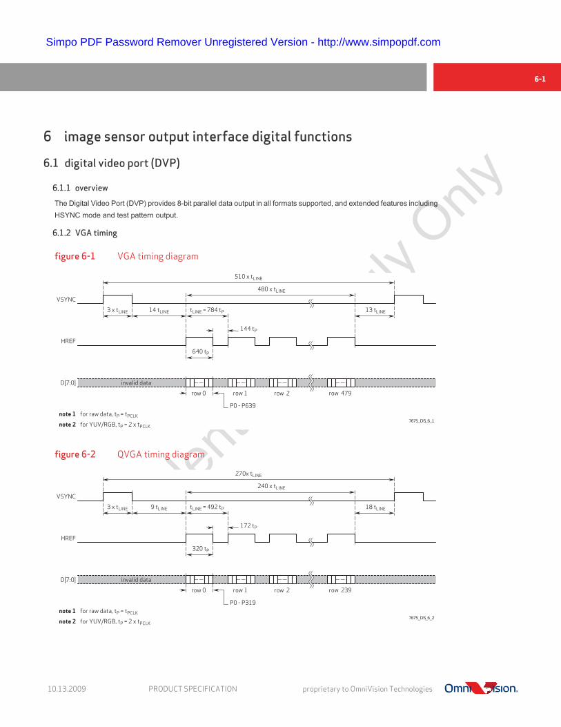
6 image sensor output interface digital functions
6.1 digital video port (DVP)
6.1.1 overview
The Digital Video Port (DVP) provides 8-bit parallel data output in all formats supported, and extended features including HSYNC mode and test pattern output.
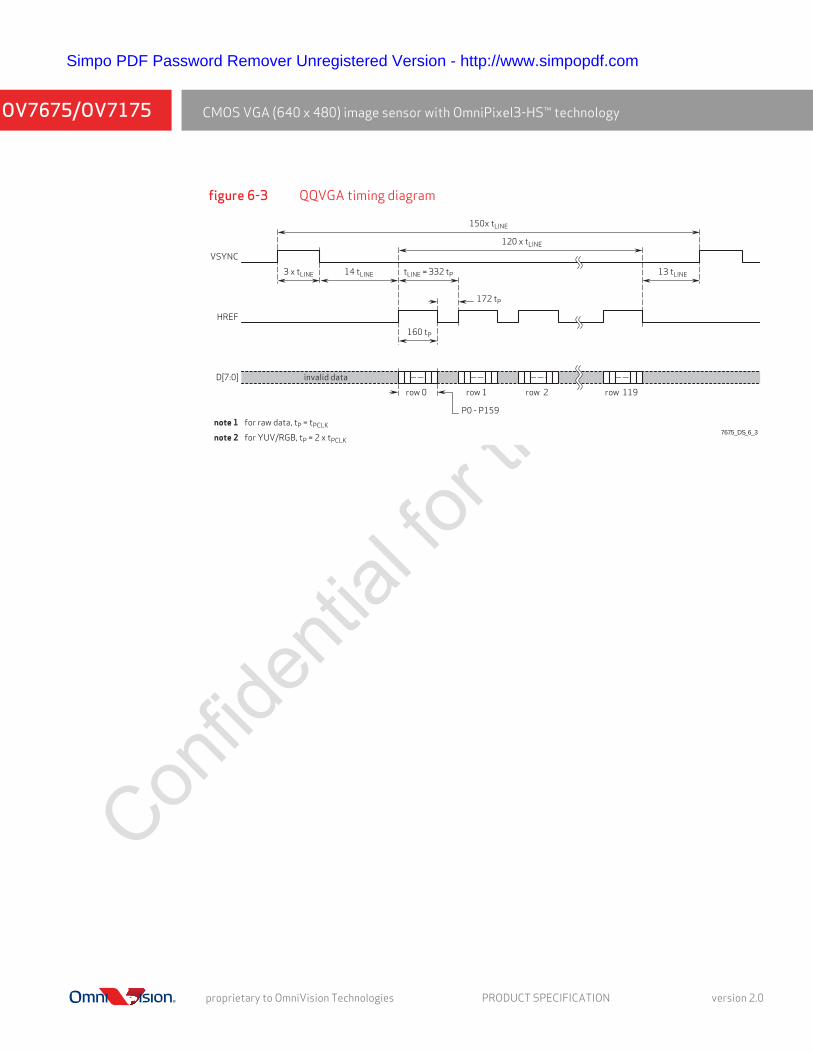
6.1.2 VGA timing
figure 6-1 VGA timing diagram.
figure 6-2 QVGA timing diagram
D[7:0]
HREF
VSYNC
note 1 for raw data, tP = tPCLK
note 2 for YUV/RGB, tP = 2 x tPCLK
510 x tLINE
3 x tLINE 14 tLINE
144 tP
P0 - P639
640 tP
row 0
invalid data
row 1 row 2 row 479
tLINE = 784 tP 13 tLINE
480 x tLINE
7675_DS_6_1
D[7:0]
HREF
VSYNC
note 1 for raw data, tP = tPCLK
note 2 for YUV/RGB, tP = 2 x tPCLK
270x tLINE
3 x tLINE 9 tLINE
172 tP
P0 - P319
320 tP
row 0
invalid data
row 1 row 2 row 239
tLINE = 492 tP 18 tLINE
240 x tLINE
7675_DS_6_2
10.13.2009 PRODUCT SPECIFICATION proprietary to OmniVision Technologies
CMOS VGA (640 x 480) image sensor with OmniPixel3-HS™ technologyOV7675/OV7175
Simpo PDF Password Remover Unregistered Version - http://www.simpopdf.com
Con
fiden
tial for
truly Only
figure 6-3 QQVGA timing diagram
D[7:0]
HREF
VSYNC
note 1 for raw data, tP = tPCLK
note 2 for YUV/RGB, tP = 2 x tPCLK
150x tLINE
3 x tLINE 14 tLINE
172 tP
P0 - P159
160 tP
row 0
invalid data
row 1 row 2 row 119
tLINE = 332 tP 13 tLINE
120 x tLINE
7675_DS_6_3
proprietary to OmniVision Technologies PRODUCT SPECIFICATION version 2.0

7-1
Simpo PDF Password Remover Unregistered Version - http://www.simpopdf.com
Con
fiden
tial for
truly Only
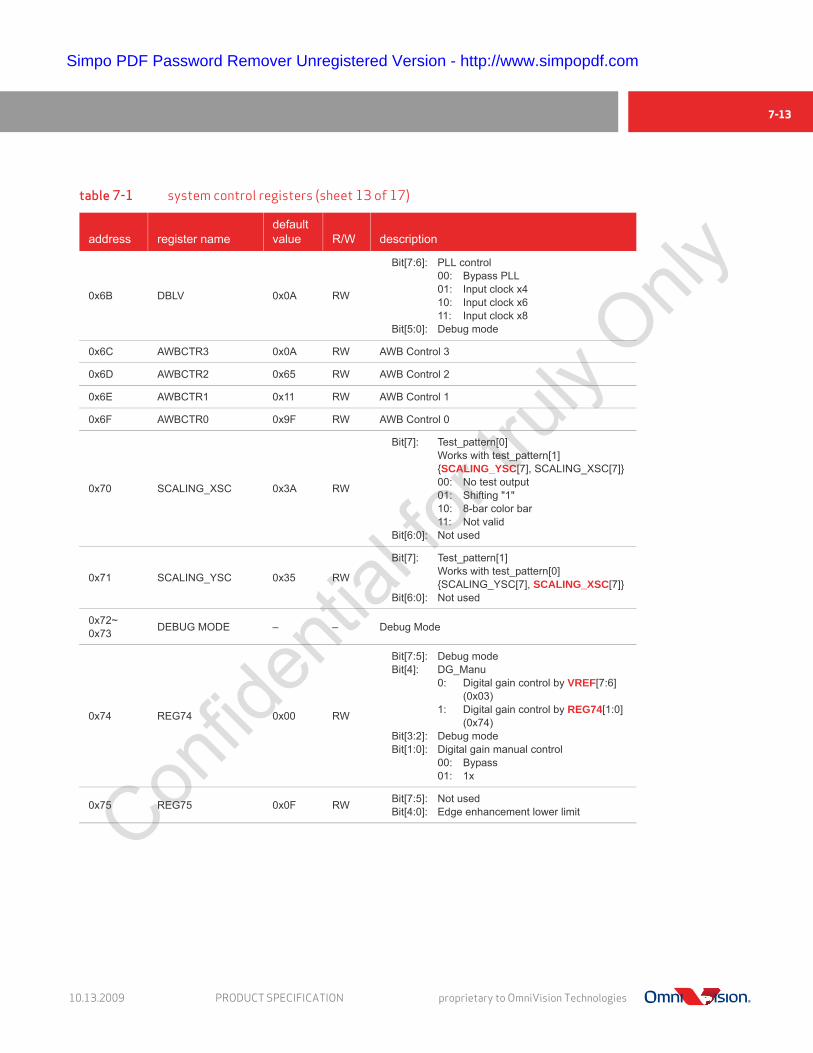
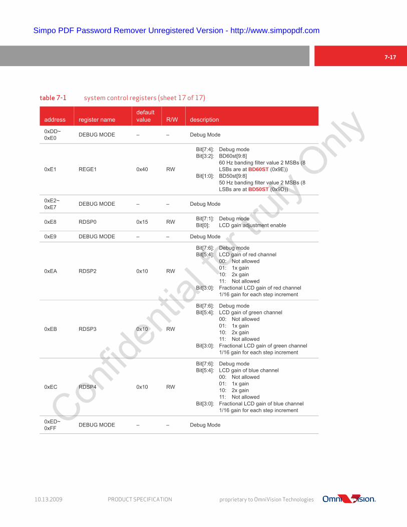
7 register tables
The following tables provide descriptions of the device control registers contained in the OV7675/OV7175. For all register enable/disable bits, enable = 1 and DISABLE = 0. The device slave addresses are 0x42 for write and 0x43 for read.
table 7-1 system control registers (sheet 1 of 17)
address
register name
default value
R/W
description
0x00 GAIN 0x00 RW
AGC - Gain Control Gain SettingBit[7:0]: AGC[7:0] (see VREF[7:6] (0x03) for
AGC[9:8])
0x01 BLUE 0x80 RW AWB – Blue Channel Gain SettingBlue Gain = BLUE[7:0] / 0x40, BLUE[7:0] ≥ 0x40
0x02 RED 0x80 RW AWB – Red Channel Gain SettingRed Gain = RED[7:0] / 0x40, RED[7:0] ≥ 0x40
0x03 VREF 0x00 RW
Vertical Frame ControlBit[7:6]: AGC[9:8] (see GAIN[7:0] (0x00) for
AGC[7:0])Bit[5:4]: Debug modeBit[3:2]: VREF end 2 LSBs (8 MSBs at
VSTART[7:0] (0x19))Bit[1:0]: VREF start 2 LSBs (8 MSBs at
VSTOP[7:0] (0x1A))
0x04 COM1 0x00 RW
Common Control 1Bit[7]: Debug modeBit[6]: CCIR656 format
0: Disable1: Enable
Bit[5:2]: Debug modeBit[1:0]: 2 LSBs (see registers AECHH[5:0]
(0x07) and AECH[7:0] (0x10) for AEC[15:10] and AEC[9:2], respectively)
0x05 BAVE 0x00 RW U/B Average LevelAutomatically updated based on chip output format
0x06 BGAVE 0x00 RW Y/Gb Average LevelAutomatically updated based on chip output format
0x07 AECHH 0x00 RW
Exposure Value - AEC 5 MSBsBit[7:6]: Not usedBit[5:0]: AEC[15:10] (see registers AECH[7:0]
(0x10) and COM1[1:0] (0x04) for AEC[9:2] and AEC[1:0], respectively)
gain = (0x03[7] + 1) x (0x03[6] + 1) x (0x00[7] + 1) (0x00[6] + 1) x
(0x00[5] + 1) x (0x00[4] + 1) x ( + 1)0x00[3:0]
16
10.13.2009 PRODUCT SPECIFICATION proprietary to OmniVision Technologies

CMOS VGA (640 x 480) image sensor with OmniPixel3-HS™ technologyOV7675/OV7175
Simpo PDF Password Remover Unregistered Version - http://www.simpopdf.com
Con
fiden
tial for
truly Only0x08 RAVE 0x00 RW V/R Average Level
Automatically updated based on chip output format
0x09 COM2 0x01 RW
Common Control 2Bit[7:5]: Debug modeBit[4]: Soft sleep mode
0: Disable1: Enable
Bit[3:2]: Debug modeBit[1:0]: Output drive capability
00: 1x01: 2x10: 3x11: 4x
0x0A PID 0x76 R Product ID Number MSB (Read only)
0x0B VER 0x73 R Product ID Number LSB (Read only)
0x0C COM3 0x00 RW
Common Control 3Bit[7]: Debug modeBit[6]: Output data MSB and LSB swapBit[5]: Tri-state option for output clock at
power-down period0: Tri-state at this period1: No tri-state at this period
Bit[4]: Tri-state option for output data at power-down period0: Tri-state at this period1: No tri-state at this period
Bit[3:0]: Debug mode
0x0D COM4 0x00 RW
Common Control 4Bit[7:6]: Debug modeBit[5:4]: Average option (must be same value as
COM17[7:6] (0x42))00: Full window01: 1/2 window10: 1/4 window11: 1/4 window
Bit[3:0]: Debug mode
0x0E DEBUG MODE – – Debug Mode
table 7-1 system control registers (sheet 2 of 17)
address
register name
default value
R/W
description
proprietary to OmniVision Technologies PRODUCT SPECIFICATION version 2.0

7-3
Simpo PDF Password Remover Unregistered Version - http://www.simpopdf.com
Con
fiden
tial for
truly Only
0x0F COM6 0x43 RW
Common Control 6Bit[7]: Output of optical black line option
0: Disable HREF at optical black1: Enable HREF at optical black
Bit[6:2]: Debug modeBit[1]: Reset all timing when format changes
0: No reset1: Resets timing
Bit[0]: Debug mode
0x10 AECH 0x40 RW
Exposure ValueBit[7:0]: AEC[9:2] (see registers AECHH[5:0]
(0x07) and COM1[1:0] (0x04) for AEC[15:10] and AEC[1:0], respectively)
0x11 CLKRC 0x80 RW
Internal ClockBit[7]: DebugBit[6]: Use external clock directly (no clock
pre-scale available)Bit[5:0]: Internal clock pre-scalar F(internal clock)
= F(input clock)/(Bit[5:0]+1)Range: [0 0000] to [1 1111]
0x12 COM7 0x00 RW
Common Control 7Bit[7]: SCCB register reset
0: No change1: Resets all registers to default
valuesBit[6:5]: Debug modeBit[4]: Output format
QVGA selectionBit[3]: Debug modeBit[2]: Output format
RGB selection (see below bit[0])Bit[1]: Color bar
0: Disable1: Enable
Bit[0]: Output formatRaw RGB (see below)
COM7[2] COM7[0]YUV 0 0RGB 1 0Bayer RAW 0 1Processed Bayer RAW 1 1
table 7-1 system control registers (sheet 3 of 17)
address
register name
default value
R/W
description
10.13.2009 PRODUCT SPECIFICATION proprietary to OmniVision Technologies

CMOS VGA (640 x 480) image sensor with OmniPixel3-HS™ technologyOV7675/OV7175
Simpo PDF Password Remover Unregistered Version - http://www.simpopdf.com
Con
fiden
tial for
truly Only
0x13 COM8 0x8F RW
Common Control 8Bit[7]: Enable fast AGC/AEC algorithmBit[6]: AEC - Step size option
0: Step size is limited to vertical blank1: Unlimited step size
Bit[5]: Banding filter ON/OFFIn order to turn ON the banding filter, BD50ST (0x9D) or BD60ST (0x9E) must be set to a non-zero value0: OFF1: ON
Bit[4]: Debug modeBit[3]: Pixel level exposure ON/OFF selection
1: Allow exposure time less than 1 line
0: Limit the minimum exposure time to 1 line
Bit[2]: AGC enable0: Disable1: Enable
Bit[1]: AWB enable0: Disable1: Enable
Bit[0]: AEC enable0: Disable1: Enable
0x14 COM9 0x4A RW
Common Control 9Bit[7]: Debug modeBit[6:4]: Automatic gain ceiling
Maximum AGC value000: 2x001: 4x010: 8x011: 16x100: 32x101 64x110: 128x111: Debug mode
Bit[3:1]: Debug modeBit[0]: Freeze AGC/AEC
table 7-1 system control registers (sheet 4 of 17)
address
register name
default value
R/W
description
proprietary to OmniVision Technologies PRODUCT SPECIFICATION version 2.0

7-5
Simpo PDF Password Remover Unregistered Version - http://www.simpopdf.com
Con
fiden
tial for
truly Only
0x15 COM10 0x00 RW
Common Control 10Bit[7]: Debug modeBit[6]: HREF changes to HSYNCBit[5]: PCLK output option
0: Free running PCLK1: PCLK does not toggle during
horizontal blankBit[4]: PCLK reverseBit[3]: HREF reverseBit[2]: VSYNC option
0: VSYNC changes on falling edge of PCLK
1: VSYNC changes on rising edge of PCLK
Bit[1]: VSYNC negativeBit[0]: HSYNC negative
0x16 NOT USED – – Not Used
0x17 HSTART 0x11 RW Output Format - Horizontal Frame (HREF column) start 8 MSBs (3 LSBs are at HREF[2:0] (0x32))
0x18 HSTOP 0x61 RW Output Format - Horizontal Frame (HREF column) end 8 MSBs (3 LSBs are at HREF[5:3] (0x32))
0x19 VSTART 0x03 RW Output Format - Vertical Frame (row) start 8 MSBs (2 LSBs are at VREF[1:0] (0x03))
0x1A VSTOP 0x7B RW Output Format - Vertical Frame (row) end 8 MSBs (2 LSBs are at VREF[3:2] (0x03))
0x1B PSHFT 0x00 RW
Data Format - Pixel Delay Select (delays timing of the D[7:0] data relative to HREF in pixel units)Range: [00] (no delay) to [FF] (256 pixel delay which accounts for whole array)
0x1C MIDH 0x7F R Manufacturer ID High Byte
0x1D MIDL 0xA2 R Manufacturer ID Low Byte
0x1E MVFP 0x01 RW
Mirror/VFlip EnableBit[7:6]: Debug modeBit[5]: Mirror
0: Normal image1: Mirror image
Bit[4]: VFlip enable0: Normal image1: Vertically flip image
Bit[3:0]: Debug mode
0x1F DEBUG MODE – – Debug Mode
table 7-1 system control registers (sheet 5 of 17)
address
register name
default value
R/W
description
10.13.2009 PRODUCT SPECIFICATION proprietary to OmniVision Technologies

CMOS VGA (640 x 480) image sensor with OmniPixel3-HS™ technologyOV7675/OV7175
Simpo PDF Password Remover Unregistered Version - http://www.simpopdf.com
Con
fiden
tial for
truly Only0x20~
0x23 NOT USED – – Not Used
0x24 AEW 0x62 RW AGC/AEC - Stable Operating Region(Upper Limit)
0x25 AEB 0x58 RW AGC/AEC - Stable Operating Region(Lower Limit)
0x26 VPT 0x93 RW
AGC/AEC Fast Mode Operating RegionBit[7:4]: High nibble of upper limit of fast mode
control zoneBit[3:0]: High nibble of lower limit of fast mode
control zone
0x27~ 0x29 NOT USED – – Not Used
0x2A EXHCH 0x00 RW
Dummy Pixel Insert Bit[7:4]: Dummy pixel insert in horizontal
direction[11:8] (2 MSBs in REGCA[7:6] (0xCA), 8 LSBs in EXHCL (0x2B))
Bit[3:2]: HSYNC falling edge delay 2 MSBs (see HSYEN[7:0] (0x31) for 8 LSBs)
Bit[1:0]: HSYNC rising edge delay 2 MSBs (see HSYST[7:0] (0x30) for 8 LSBs)
0x2B EXHCL 0x00 RW
Bit[7:0]: Dummy pixel insert in horizontal direction[7:0](see REGCA[7:6] (0xCA) and EXHCH[7:4] (0x2A))
0x2C NOT USED – – Not Used
0x2D ADVFL 0x00 RW LSBs of Insert Dummy Lines in Vertical Direction (1 bit equals 1 line)
0x2E ADVFH 0x00 RW MSBs of Insert Dummy Lines in Vertical Direction
0x2F YAVE 0x00 RW Y/G Channel Average Value
0x30 HSYST 0x08 RW HSYNC Rising Edge Delay 8 LSBs (see EXHCH[1:0] (0x2A) for 2 MSBs)
0x31 HSYEN 0x30 RW HSYNC Falling Edge Delay (see EXHCH[3:2] (0x2A) for 8 MSBs)
0x32 HREF 0x80 RW
HREF ControlBit[7:6]: HREF edge offset to data outputBit[5:3]: HREF end 3 LSBs (8 MSBs at
HSTOP (0x18))Bit[2:0]: HREF start 3 LSBs (8 MSBs at HSTART
(0x17))
table 7-1 system control registers (sheet 6 of 17)
address
register name
default value
R/W
description
proprietary to OmniVision Technologies PRODUCT SPECIFICATION version 2.0
7-7
Simpo PDF Password Remover Unregistered Version - http://www.simpopdf.com
Con
fiden
tial for
truly Only0x33~
0x39 NOT USED – – Not Used
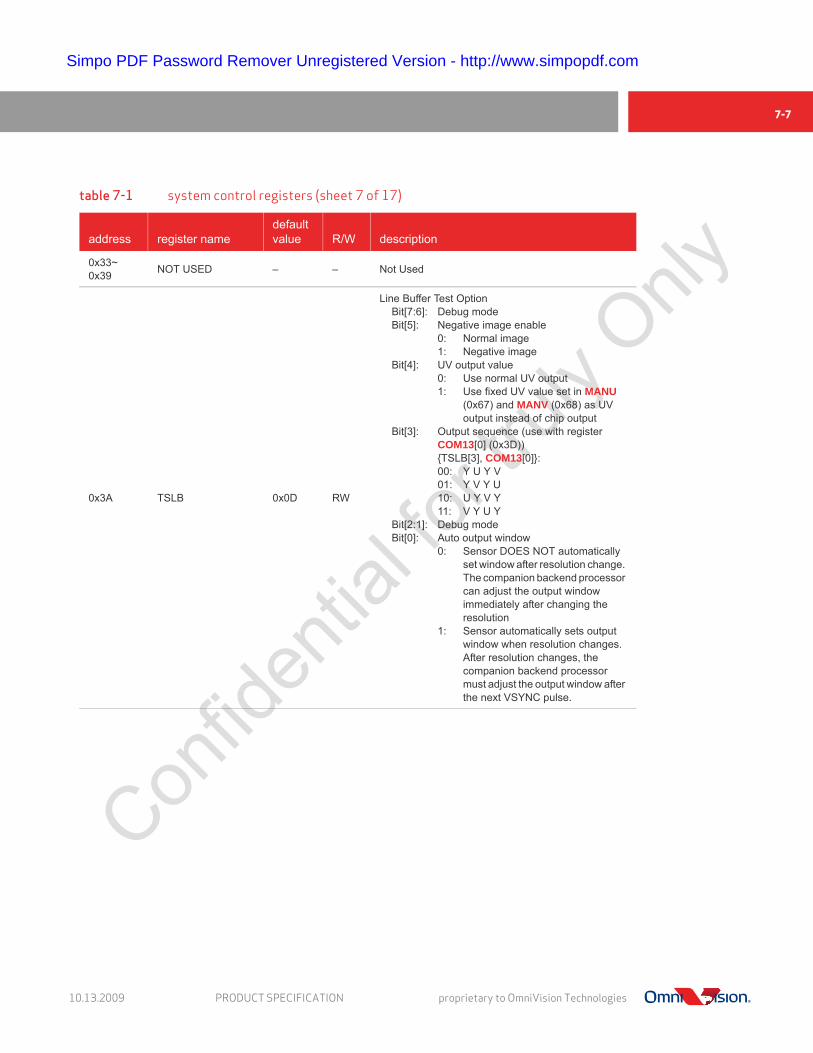
0x3A TSLB 0x0D RW
Line Buffer Test OptionBit[7:6]: Debug modeBit[5]: Negative image enable
0: Normal image1: Negative image
Bit[4]: UV output value0: Use normal UV output1: Use fixed UV value set in MANU
(0x67) and MANV (0x68) as UV output instead of chip output
Bit[3]: Output sequence (use with register COM13[0] (0x3D)){TSLB[3], COM13[0]}:00: Y U Y V01: Y V Y U10: U Y V Y11: V Y U Y
Bit[2:1]: Debug modeBit[0]: Auto output window
0: Sensor DOES NOT automatically set window after resolution change. The companion backend processor can adjust the output window immediately after changing the resolution
1: Sensor automatically sets output window when resolution changes. After resolution changes, the companion backend processor must adjust the output window after the next VSYNC pulse.
table 7-1 system control registers (sheet 7 of 17)
address
register name
default value
R/W
description
10.13.2009 PRODUCT SPECIFICATION proprietary to OmniVision Technologies
CMOS VGA (640 x 480) image sensor with OmniPixel3-HS™ technologyOV7675/OV7175
Simpo PDF Password Remover Unregistered Version - http://www.simpopdf.com
Con
fiden
tial for
truly Only
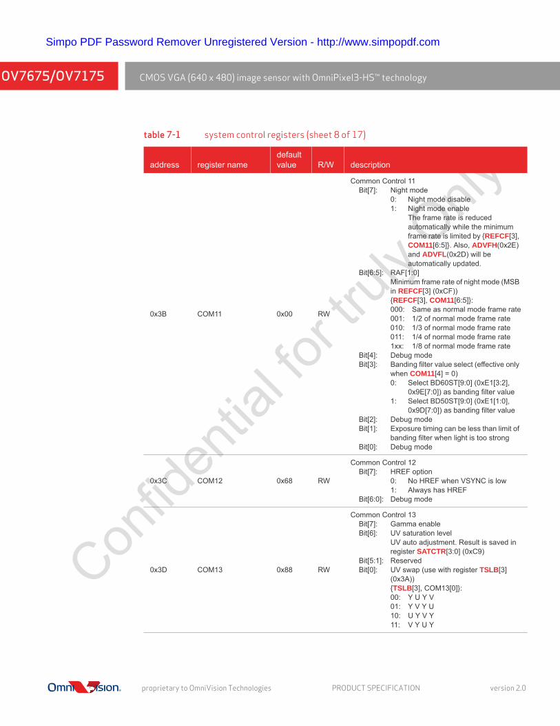
0x3B COM11 0x00 RW
Common Control 11Bit[7]: Night mode
0: Night mode disable1: Night mode enable
The frame rate is reduced automatically while the minimum frame rate is limited by {REFCF[3], COM11[6:5]}. Also, ADVFH(0x2E) and ADVFL(0x2D) will be automatically updated.
Bit[6:5]: RAF[1:0]Minimum frame rate of night mode (MSB in REFCF[3] (0xCF)){REFCF[3], COM11[6:5]}:000: Same as normal mode frame rate001: 1/2 of normal mode frame rate010: 1/3 of normal mode frame rate011: 1/4 of normal mode frame rate1xx: 1/8 of normal mode frame rate
Bit[4]: Debug modeBit[3]: Banding filter value select (effective only
when COM11[4] = 0)0: Select BD60ST[9:0] (0xE1[3:2],
0x9E[7:0]) as banding filter value1: Select BD50ST[9:0] (0xE1[1:0],
0x9D[7:0]) as banding filter valueBit[2]: Debug modeBit[1]: Exposure timing can be less than limit of
banding filter when light is too strongBit[0]: Debug mode
0x3C COM12 0x68 RW
Common Control 12Bit[7]: HREF option
0: No HREF when VSYNC is low1: Always has HREF
Bit[6:0]: Debug mode
0x3D COM13 0x88 RW
Common Control 13Bit[7]: Gamma enableBit[6]: UV saturation level
UV auto adjustment. Result is saved in register SATCTR[3:0] (0xC9)
Bit[5:1]: ReservedBit[0]: UV swap (use with register TSLB[3]
(0x3A)){TSLB[3], COM13[0]}:00: Y U Y V01: Y V Y U10: U Y V Y11: V Y U Y
table 7-1 system control registers (sheet 8 of 17)
address
register name
default value
R/W
description
proprietary to OmniVision Technologies PRODUCT SPECIFICATION version 2.0

7-9
Simpo PDF Password Remover Unregistered Version - http://www.simpopdf.com
Con
fiden
tial for
truly Only
0x3E COM14 0x00 RW
Common Control 14Bit[7:5]: Debug modeBit[4]: DCW and scaling PCLK enable
0: Normal PCLK1: PCLK controlled by register
COM14[2:0] Bit[3]: Debug modeBit[2:0]: PCLK divider
(only when COM14[4] = 1)000: Divided by 1001: Divided by 2010: Divided by 4011: Divided by 8100: Divided by 16101~111: Debug mode
0x3F EDGE 0x00 RWEdge Enhancement Adjustment
Bit[7:5]: Debug modeBit[4:0]: Edge enhancement factor
0x40 COM15 0xC0 RW
Common Control 15Bit[7:6]: Data format
Output full range enable0x: Output range: [10] to [F0]10: Output range: [01] to [FE]11: Output range: [00] to [FF]
Bit[5:4]: RGB555/565 option (must set COM7[2] = 1 and COM7[0] = 0)x0: Normal RGB output01: RGB565, effective only when
REG444[1] (0x8C) is low11: RGB555, effective only when
REG444[1] (0x8C) is lowBit[3:0]: Debug mode
table 7-1 system control registers (sheet 9 of 17)
address
register name
default value
R/W
description
10.13.2009 PRODUCT SPECIFICATION proprietary to OmniVision Technologies

CMOS VGA (640 x 480) image sensor with OmniPixel3-HS™ technologyOV7675/OV7175
Simpo PDF Password Remover Unregistered Version - http://www.simpopdf.com
Con
fiden
tial for
truly Only
0x41 COM16 0x38 RW
Common Control 16Bit[7:6]: Debug modeBit[5]: Enable edge enhancement threshold
auto-adjustment for YUV output (result is saved in register EDGE[4:0] (0x3F) and range is controlled by registers REG75REG75[4:0] (0x75) and REG76[4:0] (0x76))0: Disable1: Enable
Bit[4]: De-noise threshold auto-adjustment (result is saved in register DNSTH (0x4C) and range is controlled by REG77[7:0] (0x77)0: Disable1: Enable
Bit[3]: AWB gain enableBit[2]: ReservedBit[1]: Color matrix coefficient double option
0: Original matrix1: Double of original matrix
Bit[0]: Debug mode
0x42 COM17 0x00 RW
Common Control 17Bit[7:6]: AEC window (must be the same value as
COM4[5:4] (0x0D))00: Normal01: 1/210: 1/411: 1/4
Bit[5:4]: Debug modeBit[3]: DSP color bar enable
0: Disable1: Enable
Bit[2:0]: Debug mode
0x43~ 0x4B DEBUG MODE – – Debug Mode
0x4C DNSTH 0x00 RW De-noise Strength
0x4D~ 0x4E DEBUG MODE – – Debug Mode
0x4F MTX1 0x96 RW Matrix Coefficient 1
0x50 MTX2 0x9B RW Matrix Coefficient 2
0x51 MTX3 0x05 RW Matrix Coefficient 3
0x52 MTX4 0x1A RW Matrix Coefficient 4
0x53 MTX5 0x7F RW Matrix Coefficient 5
table 7-1 system control registers (sheet 10 of 17)
address
register name
default value
R/W
description
proprietary to OmniVision Technologies PRODUCT SPECIFICATION version 2.0

7-11
Simpo PDF Password Remover Unregistered Version - http://www.simpopdf.com
Con
fiden
tial for
truly Only0x54 MTX6 0x54 RW Matrix Coefficient 6
0x55 BRIGHT 0x00 RW Brightness Control
0x56 CONTRAS 0x40 RW Contrast Control
0x57 CONTRAS CENTER 0x80 RW Contrast Center
0x58 MTXS 0x1A RW
Bit[7]: Auto contrast center enable0: Disable, center is set by register
CONTRAS CENTER (0x57)1: Enable, register CONTRAS
CENTER is updated automaticallyBit[6]: Debug modeBit[5]: Sign bit for MTX6 (0x54)Bit[4]: Sign bit for MTX5 (0x53)Bit[3]: Sign bit for MTX4 (0x52)Bit[2]: Sign bit for MTX3 (0x51)Bit[1]: Sign bit for MTX2 (0x50)Bit[0]: Sign bit for MTX1 (0x4F)
0x59~ 0x61 DEBUG MODE – – Debug Mode
0x62 LCC1 0x00 RW
Lens Correction Option 1Bit[7]: Sign bit for X coordinate of lens
correction center relative to array center0: Coordinate is positive1: Coordinate is negative
Bit[6:0]: X coordinate of lens correction center relative to array center
0x63 LCC2 0x00 RW
Lens Correction Option 2Bit[7]: Sign bit for Y coordinate of lens
correction center relative to array center0: Coordinate is positive1: Coordinate is negative
Bit[6:0]: Y coordinate of lens correction center relative to array center
0x64 LCC3 0x50 RW
Lens Correction Option 3Bit[2]: When LCC5[2] (0x66) is 1, this is the G
channel compensation coefficientWhen LCC5[2] (0x66) is 0, this is the R, G and B channel compensation coefficient
0x65 LCC4 0x30 RW Lens Correction Option 4 - Radius of the circular section where no compensation applies
table 7-1 system control registers (sheet 11 of 17)
address
register name
default value
R/W
description
10.13.2009 PRODUCT SPECIFICATION proprietary to OmniVision Technologies
CMOS VGA (640 x 480) image sensor with OmniPixel3-HS™ technologyOV7675/OV7175
Simpo PDF Password Remover Unregistered Version - http://www.simpopdf.com
Con
fiden
tial for
truly Only
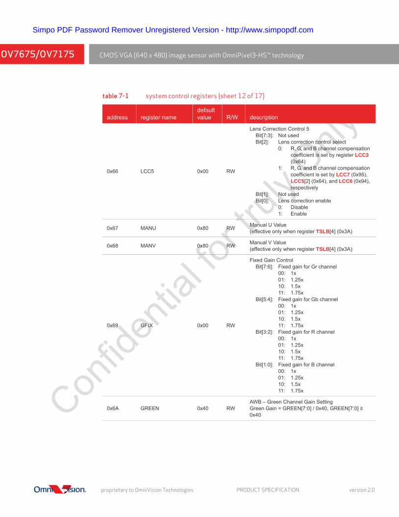
0x66 LCC5 0x00 RW
Lens Correction Control 5Bit[7:3]: Not usedBit[2]: Lens correction control select
0: R, G, and B channel compensation coefficient is set by register LCC3 (0x64)
1: R, G, and B channel compensation coefficient is set by LCC7 (0x95), LCC5[2] (0x64), and LCC6 (0x94), respectively
Bit[1]: Not usedBit[0]: Lens correction enable
0: Disable1: Enable
0x67 MANU 0x80 RW Manual U Value(effective only when register TSLB[4] (0x3A)
0x68 MANV 0x80 RW Manual V Value(effective only when register TSLB[4] (0x3A)
0x69 GFIX 0x00 RW
Fixed Gain ControlBit[7:6]: Fixed gain for Gr channel
00: 1x01: 1.25x10: 1.5x11: 1.75x
Bit[5:4]: Fixed gain for Gb channel00: 1x01: 1.25x10: 1.5x11: 1.75x
Bit[3:2]: Fixed gain for R channel00: 1x01: 1.25x10: 1.5x11: 1.75x
Bit[1:0]: Fixed gain for B channel00: 1x01: 1.25x10: 1.5x11: 1.75x
0x6A GREEN 0x40 RWAWB – Green Channel Gain SettingGreen Gain = GREEN[7:0] / 0x40, GREEN[7:0] ≥ 0x40
table 7-1 system control registers (sheet 12 of 17)
address
register name
default value
R/W
description
proprietary to OmniVision Technologies PRODUCT SPECIFICATION version 2.0
7-13
Simpo PDF Password Remover Unregistered Version - http://www.simpopdf.com
Con
fiden
tial for
truly Only
0x6B DBLV 0x0A RW
Bit[7:6]: PLL control00: Bypass PLL01: Input clock x410: Input clock x611: Input clock x8
Bit[5:0]: Debug mode
0x6C AWBCTR3 0x0A RW AWB Control 3
0x6D AWBCTR2 0x65 RW AWB Control 2
0x6E AWBCTR1 0x11 RW AWB Control 1
0x6F AWBCTR0 0x9F RW AWB Control 0
0x70 SCALING_XSC 0x3A RW
Bit[7]: Test_pattern[0]Works with test_pattern[1] {SCALING_YSC[7], SCALING_XSC[7]}00: No test output01: Shifting "1"10: 8-bar color bar11: Not valid
Bit[6:0]: Not used
0x71 SCALING_YSC 0x35 RW
Bit[7]: Test_pattern[1]Works with test_pattern[0] {SCALING_YSC[7], SCALING_XSC[7]}
Bit[6:0]: Not used
0x72~ 0x73 DEBUG MODE – – Debug Mode
0x74 REG74 0x00 RW
Bit[7:5]: Debug modeBit[4]: DG_Manu
0: Digital gain control by VREF[7:6] (0x03)
1: Digital gain control by REG74[1:0] (0x74)
Bit[3:2]: Debug modeBit[1:0]: Digital gain manual control
00: Bypass01: 1x
0x75 REG75 0x0F RW Bit[7:5]: Not usedBit[4:0]: Edge enhancement lower limit
table 7-1 system control registers (sheet 13 of 17)
address
register name
default value
R/W
description
10.13.2009 PRODUCT SPECIFICATION proprietary to OmniVision Technologies

CMOS VGA (640 x 480) image sensor with OmniPixel3-HS™ technologyOV7675/OV7175
Simpo PDF Password Remover Unregistered Version - http://www.simpopdf.com
Con
fiden
tial for
truly Only
0x76 REG76 0x01 RW
Bit[7]: Black pixel correction enable0: Disable1: Enable
Bit[6]: White pixel correction enable0: Disable1: Enable
Bit[5]: Not usedBit[4:0]: Edge enhancement higher limit
0x77 REG77 0x10 RW Bit[7:0]: De-noise offset
0x78~ 0x79 DEBUG MODE – – Debug Mode
0x7A SLOP 0x28 RWGamma Curve Highest Segment SlopeCalculated as follows:SLOP[7:0] = (0x100 - GAM15[7:0]) x 4/3
0x7B GAM1 0x04 RW Gamma Curve 1st Segment Input End Point 0x04 Output Value
0x7C GAM2 0x09 RW Gamma Curve 2nd Segment Input End Point 0x08 Output Value
0x7D GAM3 0x16 RW Gamma Curve 3rd Segment Input End Point 0x10 Output Value
0x7E GAM4 0x30 RW Gamma Curve 4th Segment Input End Point 0x20 Output Value
0x7F GAM5 0x3E RW Gamma Curve 5th Segment Input End Point 0x28 Output Value
0x80 GAM6 0x4B RW Gamma Curve 6th Segment Input End Point 0x30 Output Value
0x81 GAM7 0x59 RW Gamma Curve 7th Segment Input End Point 0x38 Output Value
0x82 GAM8 0x67 RW Gamma Curve 8th Segment Input End Point 0x40 Output Value
0x83 GAM9 0x72 RW Gamma Curve 9th Segment Input End Point 0x48 Output Value
0x84 GAM10 0x7C RW Gamma Curve 10th Segment Input End Point 0x50 Output Value
0x85 GAM11 0x8E RW Gamma Curve 11th Segment Input End Point 0x60 Output Value
0x86 GAM12 0x9E RW Gamma Curve 12th Segment Input End Point 0x70 Output Value
table 7-1 system control registers (sheet 14 of 17)
address
register name
default value
R/W
description
proprietary to OmniVision Technologies PRODUCT SPECIFICATION version 2.0

7-15
Simpo PDF Password Remover Unregistered Version - http://www.simpopdf.com
Con
fiden
tial for
truly Only0x87 GAM13 0xB6 RW Gamma Curve 13th Segment Input End Point 0x90
Output Value
0x88 GAM14 0xCC RW Gamma Curve 14th Segment Input End Point 0xB0 Output Value
0x89 GAM15 0xE2 RW Gamma Curve 15th Segment Input End Point 0xD0 Output Value
0x8A~ 0x8B DEBUG MODE – – Debug Mode
0x8C REG444 0x00 RW
Bit[7:2]: Not usedBit[1]: RGB444 enable (effective only when
COM15[4] (0x40) is high)0: Disable1: Enable
Bit[0]: RGB444 word format0: xR GB1: RG Bx
0x8D~ 0x91 DEBUG MODE – – Debug Mode
0x92 DM_LNH 0x00 RW Dummy Line 8 LSBs
0x93 LCC6 0x50 RW Dummy Line 8 MSBs
0x94 LCC7 0x50 RW Lens Correction Option 6 (effective only when LCC5[2] (0x66) is high)
0x95 RSVD XX – Lens Correction Option 7 (effective only when LCC5[2] (0x66) is high)
0x96~ 0x9C DEBUG MODE – – Debug Mode
0x9D BD50ST 0x7F RW50 Hz Banding Filter Value, LSBs (effective only when COM8[5] (0x13) is high and COM11[3] (0x3B) is high)
0x9E BD60ST 0xC0 RW60 Hz Banding Filter Value, LSBs (effective only when COM8[5] (0x13) is high and COM11[3] (0x3B) is low)
0x9F~ 0xA3 DEBUG MODE – – Debug Mode
table 7-1 system control registers (sheet 15 of 17)
address
register name
default value
R/W
description
10.13.2009 PRODUCT SPECIFICATION proprietary to OmniVision Technologies

CMOS VGA (640 x 480) image sensor with OmniPixel3-HS™ technologyOV7675/OV7175
Simpo PDF Password Remover Unregistered Version - http://www.simpopdf.com
Con
fiden
tial for
truly Only
0xA4 NT_CTRL 0x00 RW
Bit[7:4]: Not usedBit[3]: Auto frame rate adjustment control
0: Double exposure time1: Reduce frame rate by half
Bit[2]: Not usedBit[1:0]: Auto frame rate adjustment switch point
00: Insert dummy row at 2x gain01: Insert dummy row at 4x gain10: Insert dummy row at 8x gain
0xA5 BD50MAX 0x0F RW 50Hz Banding Step Limit
0xA6 – 0xAA DEBUG MODE – – Debug Mode
0xAB BD60MAX 0x0F RW 60Hz Banding Step Limit
0xAC – 0xC8 DEBUG MODE – – Debug Mode
0xC9 SATCTR 0xC0 RWSaturation Control
Bit[7:4]: UV saturation control minBit[3:0]: UV saturation control result
0xCA REGCA 0x00 RW
Bit[7:6]: Dummy pixel insert in horizontal direction[13:12] (see EXHCH[7:4] (0x2A) and EXHCL[7:0] (0x2B))
Bit[7:6]: Debug mode
0xCB – 0xCE NOT USED – – Not used
0xCF REFCF 0x84 RW
Bit[7:4]: Debug modeBit[3]: RAF[2] (used together with COM11[6:5]
(0x3B))Bit[2:0]: Debug mode
0xD0~ 0xD3 DEBUG MODE – – Debug Mode
0xD4 RADCO 0x84 RW
ADC ControlBit[7:3]: Debug modeBit[2:0]: ADC referenced adjustment
000: 0.8x100: 1x111: 1.2x
0xD5~ 0xDB DEBUG MODE – – Debug Mode
0xDC RPWC2 0x35 RW
Bit[7:4]: Debug modeBit[3]: Regulator control
0: Enable internal regulator1: Bypass internal regulator
table 7-1 system control registers (sheet 16 of 17)
address
register name
default value
R/W
description
proprietary to OmniVision Technologies PRODUCT SPECIFICATION version 2.0
7-17
Simpo PDF Password Remover Unregistered Version - http://www.simpopdf.com
Con
fiden
tial for
truly Only0xDD~
0xE0 DEBUG MODE – – Debug Mode
0xE1 REGE1 0x40 RW
Bit[7:4]: Debug modeBit[3:2]: BD60st[9:8]
60 Hz banding filter value 2 MSBs (8 LSBs are at BD60ST (0x9E))
Bit[1:0]: BD50st[9:8]50 Hz banding filter value 2 MSBs (8 LSBs are at BD50ST (0x9D))
0xE2~ 0xE7 DEBUG MODE – – Debug Mode
0xE8 RDSP0 0x15 RW Bit[7:1]: Debug modeBit[0]: LCD gain adjustment enable
0xE9 DEBUG MODE – – Debug Mode
0xEA RDSP2 0x10 RW
Bit[7:6]: Debug modeBit[5:4]: LCD gain of red channel
00: Not allowed01: 1x gain10: 2x gain11: Not allowed
Bit[3:0]: Fractional LCD gain of red channel1/16 gain for each step increment
0xEB RDSP3 0x10 RW
Bit[7:6]: Debug modeBit[5:4]: LCD gain of green channel
00: Not allowed01: 1x gain10: 2x gain11: Not allowed
Bit[3:0]: Fractional LCD gain of green channel1/16 gain for each step increment
0xEC RDSP4 0x10 RW
Bit[7:6]: Debug modeBit[5:4]: LCD gain of blue channel
00: Not allowed01: 1x gain10: 2x gain11: Not allowed
Bit[3:0]: Fractional LCD gain of blue channel1/16 gain for each step increment
0xED~ 0xFF DEBUG MODE – – Debug Mode
table 7-1 system control registers (sheet 17 of 17)
address
register name
default value
R/W
description
10.13.2009 PRODUCT SPECIFICATION proprietary to OmniVision Technologies

CMOS VGA (640 x 480) image sensor with OmniPixel3-HS™ technologyOV7675/OV7175
Simpo PDF Password Remover Unregistered Version - http://www.simpopdf.com
Con
fiden
tial for
truly Only
proprietary to OmniVision Technologies PRODUCT SPECIFICATION version 2.0

8-1
Simpo PDF Password Remover Unregistered Version - http://www.simpopdf.com
Con
fiden
tial for
truly Only
8 operating specifications
8.1 absolute maximum ratings
8.2 functional temperature
table 8-1 absolute maximum ratings
parameter absolute maximum ratinga
a. exceeding the absolute maximum ratings shown above invalidates all AC and DC electrical specifications and may result in permanent damage to the device. Exposure to absolute maximum rated conditions for extended periods may affect device reliability.
ambient storage temperature -40°C to +95°C
supply voltage (with respect to ground)VDD-A 4.5V
VDD-IO 4.5V
electro-static discharge (ESD)human body model 2000V
machine model 200V
all input/output voltages (with respect to ground) -0.3V to VDD-IO + 1V
I/O current on any input or output pin + 200 mA
peak solder temperature (10 second dwell time) 245°C
table 8-2 functional temperature
parameter range
operating temperature rangea
a. sensor functions but image quality may be noticeably different at temperatures outside of stable image range
-30°C to +70°C
stable image temperature rangeb
b. image quality remains stable throughout this temperature range
0°C to 50°C
10.13.2009 PRODUCT SPECIFICATION proprietary to OmniVision Technologies

CMOS VGA (640 x 480) image sensor with OmniPixel3-HS™ technologyOV7675/OV7175
Simpo PDF Password Remover Unregistered Version - http://www.simpopdf.com
Con
fiden
tial for
truly Only
8.3 DC characteristics
table 8-3 DC characteristics (-30°C < TA < 70°C)
symbol parameter min typ max unit
supply
VDD-A supply voltage (analog) 2.6 2.8 3.0 V
VDD-IO supply voltage (digital I/O) 1.71 2.8 3.0 V
IDD-Aactive (operating) current
13 20 mA
IDD-IO 22 30 mA
IDDS-SCCBstandby current
1 2 mA
IDDS-PWDN 20 50 µA
digital inputs (typical conditions: AVDD = 2.8V, DOVDD = 2.8V)
VIL input voltage LOW 0.84 V
VIH input voltage HIGH 1.96 V
CIN input capacitor 10 pF
digital outputs (standard loading 25 pF)
VOH output voltage HIGH 2.52 V
VOL output voltage LOW 0.28 V
serial interface inputs
VILa
a. based on DOVDD = 2.8 V
SCL and SDA -0.5 0 0.84 V
VIHa SCL and SDA 1.96 2.8 3.3 V
proprietary to OmniVision Technologies PRODUCT SPECIFICATION version 2.0

8-3
Simpo PDF Password Remover Unregistered Version - http://www.simpopdf.com
Con
fiden
tial for
truly Only
8.4 AC characteristics
table 8-4 AC characteristics (TA = 25°C, VDD-A = 2.8V, VDD-IO = 2.8V)
symbol parameter min typ max unit
ADC parameters
B analog bandwidth 12 MHz
DLE DC differential linearity error 0.5 LSB
ILE DC integral linearity error 1 LSB
setting time for hardware reset <1 ms
setting time for software reset <1 ms
setting time for resolution mode change <1 ms
setting time for register setting <300 ms
table 8-5 timing characteristics
symbol parameter min typ max unit
oscillator and clock input
fOSC frequency (XVCLK) 1.5a
a. below 6 MHz, PLL should be by-passed
24 27 MHz
tr, tf clock input rise/fall time 5 (10b)
b. if using the internal PLL
ns
10.13.2009 PRODUCT SPECIFICATION proprietary to OmniVision Technologies
CMOS VGA (640 x 480) image sensor with OmniPixel3-HS™ technologyOV7675/OV7175
Simpo PDF Password Remover Unregistered Version - http://www.simpopdf.com
Con
fiden
tial for
truly Only
proprietary to OmniVision Technologies PRODUCT SPECIFICATION version 2.0

9-1
Simpo PDF Password Remover Unregistered Version - http://www.simpopdf.com
Con
fiden
tial for
truly Only
9 mechanical specifications
9.1 physical specifications
figure 9-1 package specifications
table 9-1 package dimensions
parameter symbol min typ max unit
package body dimension x A 2790 2815 2840 µm
package body dimension y B 2800 2825 250 µm
package height C 690 750 810 µm
ball height C1 100 130 160 µm
package body thickness C2 575 620 665 µm
thickness of glass surface to wafer C3 425 445 465 µm
ball diameter D 220 250 280 µm
total pin count N 23 (2 NC)
pin count x-axis N1 5
pin count y-axis N2 5
pins pitch x-axis J1 500 µm
pins pitch y-axis J2 500 µm
edge-to-pin center distance analog x S1 408 438 µm
edge-to-pin center distance analog y S2 413 443 µm
1234554321
ABCD
7675_CSP_DS_9_1
E
A
A
BCDE
J1S1
BJ2
S2
bottom view(bumps up)
top view(bumps down)
C2
C1
glass die
CC3
side view
D
center of BGA (die) =center of the package
X Y ZWB C DA
10.13.2009 PRODUCT SPECIFICATION proprietary to OmniVision Technologies
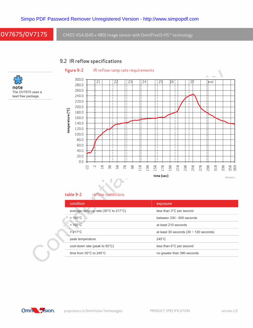
CMOS VGA (640 x 480) image sensor with OmniPixel3-HS™ technologyOV7675/OV7175
Simpo PDF Password Remover Unregistered Version - http://www.simpopdf.com
Con
fiden
tial for
truly Only
9.2 IR reflow specifications
figure 9-2 IR reflow ramp rate requirements
note The OV7675 uses a lead free package.
table 9-2 reflow conditions
condition exposure
average ramp-up rate (30°C to 217°C) less than 3°C per second
> 100°C between 330 - 600 seconds
> 150°C at least 210 seconds
> 217°C at least 30 seconds (30 ~ 120 seconds)
peak temperature 245°C
cool-down rate (peak to 50°C) less than 6°C per second
time from 30°C to 245°C no greater than 390 seconds
time (sec)
tem
per
atu
re (
°C)
-22 -2 18
38
58
78
98
11
8
13
8
15
8
17
8
35
8
33
8
31
8
29
8
27
8
25
8
23
8
21
8
19
8
36
9
0.0
300.0
280.0
220.0
240.0
260.0
200.0
180.0
140.0
160.0
120.0
100.0
80.0
60.0
40.0
20.0
Z1 Z2 Z3 Z4 Z5 Z6 Z7 end
7675 DS 9 2
proprietary to OmniVision Technologies PRODUCT SPECIFICATION version 2.0
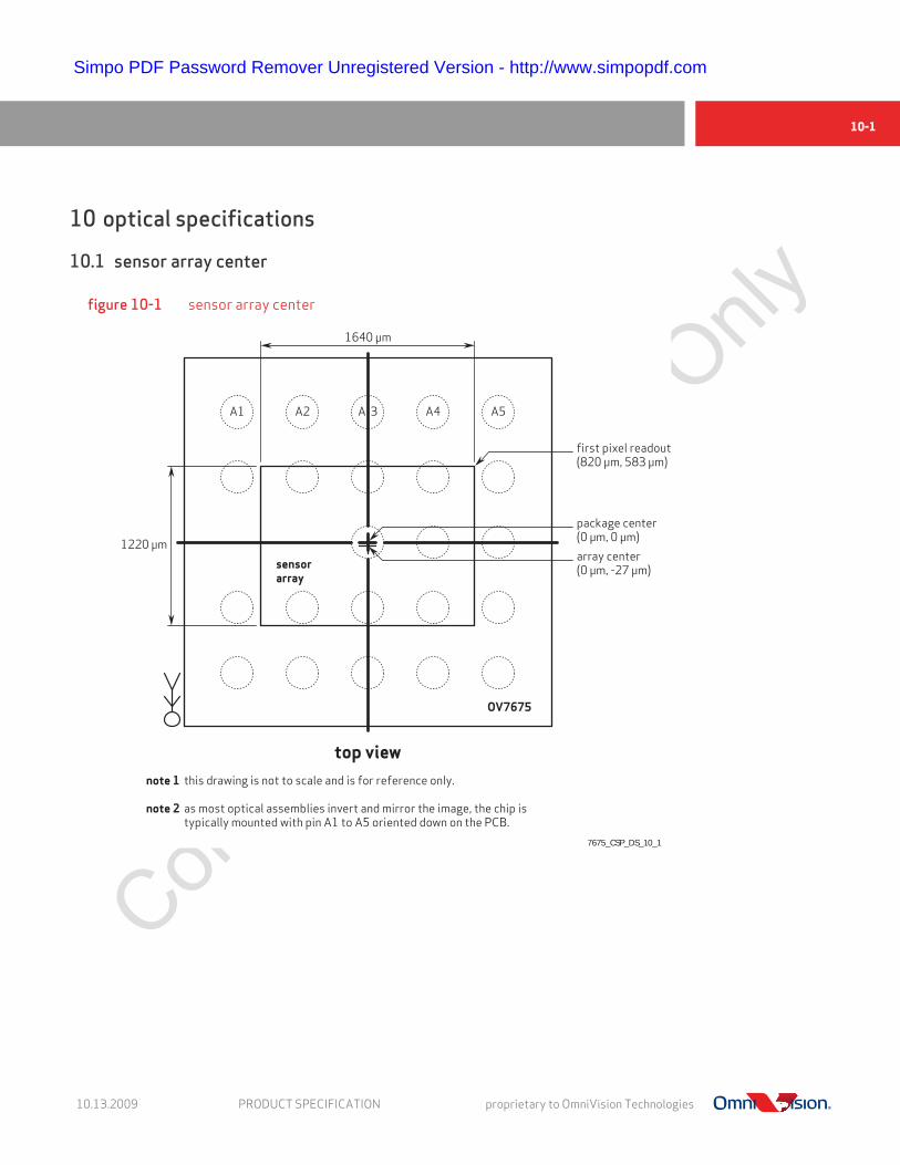
10-1
Simpo PDF Password Remover Unregistered Version - http://www.simpopdf.com
Con
fiden
tial for
truly Only
10 optical specifications
10.1 sensor array center
figure 10-1 sensor array center
1640 μm
1220 μmarray center(0 μm, -27 μm)
package center(0 μm, 0 μm)
first pixel readout(820 μm, 583 μm)
OV7675
sensorarray
note 1
note 2
this drawing is not to scale and is for reference only.
as most optical assemblies invert and mirror the image, the chip istypically mounted with pin A1 to A5 oriented down on the PCB.
top view
A1 A2 A 3 A4 A5
7675_CSP_DS_10_1
10.13.2009 PRODUCT SPECIFICATION proprietary to OmniVision Technologies

CMOS VGA (640 x 480) image sensor with OmniPixel3-HS™ technologyOV7675/OV7175
Simpo PDF Password Remover Unregistered Version - http://www.simpopdf.com
Con
fiden
tial for
truly Only
10.2 lens chief ray angle (CRA)
figure 10-2 chief ray angle (CRA)
table 10-1 CRA versus image height plot
field (%) image height (mm) CRA (degrees) maximum +4 minimum -4
0 0 0 4 -4
0.1 0.1 1.4117 5.4117 -2.5883
0.2 0.2 2.9752 6.9752 -1.0248
0.3 0.3 4.7348 8.7348 0.7348
0.4 0.4 6.6999 10.6999 2.6999
0.5 0.5 8.8546 12.8546 4.8546
0.6 0.6 11.1558 15.1558 7.1558
0.7 0.7 13.5627 17.5627 9.5627
0.8 0.8 16.0498 20.0498 12.0498
0.9 0.9 18.601 22.601 14.601
1.0 1.0 21.2001 25.2001 17.2001
0.0
0.1
0.2
0.3
0.4
0.5
0.6
0.7
0.8
0.9
1.0
-5.0
0.0
5.0
10.0
15.0
20.0
25.0
30.0
min (-4)
image height (mm)
CRA
(deg
ree)
CRAmax (+4)
7675_DS_10_2
proprietary to OmniVision Technologies PRODUCT SPECIFICATION version 2.0

rev-1
Simpo PDF Password Remover Unregistered Version - http://www.simpopdf.com
Con
fiden
tial for
truly Only
revision history
version 1.0 05.14.2009
• initial release
version 2.0 10.13.2009
• changed preliminary specification to product specification
• in the key specifications section made changes to: power requirements, sensitivity, S/N ration, dynamic range, maximum exposure interval, dark current, well capacity and fixed pattern noise
• in chapter 7, updated the default value for registers 0x24, 0x25, 0x26, 0x41, 0x4F, 0x50, 0x51, 0x52, 0x53, 0x54, 0x58, 0x6A, 0x6C, 0x6D, 0x6E, 0x6F, 0x7A~0x89, 0xCF
• in chapter 8, updated the TBD values in table 8-2
• in chapter 8, removed figure 8-1 and table 8-5
10.13.2009 PRODUCT SPECIFICATION proprietary to OmniVision Technologies

CMOS VGA (640 x 480) image sensor with OmniPixel3-HS™ technologyOV7675/OV7175
Simpo PDF Password Remover Unregistered Version - http://www.simpopdf.com
Con
fiden
tial for
truly Only
proprietary to OmniVision Technologies PRODUCT SPECIFICATION version 2.0

Con
fiden
tial for
truly Only
Simpo PDF Password Remover Unregistered Version - http://www.simpopdf.com
entia
l for
truly Onlythe clear advantage™
Simpo PDF Password Remover Unregistered Version - http://www.simpopdf.com
idOmniVision Technologies, Inc.
Con
UNITED STATES
4275 Burton DriveSanta Clara, CA 95054
tel: + 1 408 567 3000
fax: + 1 408 567 3001
email: [email protected]
UNITED KINGDOM
Hampshire + 44 1256 744 610
website: www.ovt.com
fFINLAND
Mouhijärvi + 358 3 341 1898
GERMANY
Munich +49 89 63 81 99 88
CHINA
Beijing + 86 10 6580 1690
Shanghai + 86 21 6105 5100
Shenzhen + 86 755 8384 9733
Hong Kong + 852 2403 4011
JAPAN
Tokyo + 81 3 5765 6321
KOREA
Seoul + 82 2 3478 2812
SINGAPORE + 65 6562 8250
TAIWAN
Taipei + 886 2 2657 9800 - ext.#100