Embed Size (px)
Citation preview
Instruction
Contents
Chapter 1: PLC Ladder Diagram and the Coding Rules of Mnemonic
1.1 The Operation Principle of Ladder Diagram............................................................. 1-1
1.1.1 Combination Logic ................................................................................................. 1-1
1.1.2 Sequential Logic .................................................................................................... 1-2
1.2 Differences Between the Conventional and PLC Ladder Diagram .......................... 1-3
1.3 Ladder Diagram Structure and Terminology ............................................................ 1-5
1.4 The Coding Rules of Mnemonic ............................................................................... 1-8
1.5 The De-Composition of a Network.............................................................................. 1-11
1.6 Using Temporary Relays.......................................................................................... 1-12
1.7 Program Simplification Techniques.......................................................................... 1-13
Chapter 2: FBS-PLC Memory Allocation
2.1 FBS-PLC Memory Allocation .................................................................................... 2-1
2.2 Digital and Register Allocations................................................................................ 2-2
2.3 Special Relay Details ............................................................................................... 2-3
2.4 Special Registers Details ......................................................................................... 2-8
Chapter 3: FBS-PLC Instruction Lists
3.1 Sequential Instructions............................................................................................. 3-1
3.2 Function Instructions ................................................................................................ 3-2
Chapter 4: Sequential Instructions
4.1 Valid range of the Operand of Sequential Instructions............................................. 4-1
4.2 Element Description ................................................................................................. 4-2
4.2.1 Characteristics of A, B, TU and TD Contacts ............................................................ 4-2
4.2.2 OPEN and SHORT Contact .................................................................................... 4-3
4.2.3 Output Coil and Inverse Output Coil ......................................................................... 4-4
4.2.4 Retentive Output Coil ............................................................................................. 4-4
4.2.5 Set Coil and Reset Coil........................................................................................... 4-5
4.3 Node Operation Instructions..................................................................................... 4-5
Chapter 5: Description of Function Instructions
5.1 The Format of Function Instructions......................................................................... 5-1
5.1.1 Input Control.......................................................................................................... 5-1
5.1.2 Instruction Number and Derivative Instructions ......................................................... 5-2
5.1.3 Operand................................................................................................................ 5-3
5.1.4 Functions Output (FO)............................................................................................ 5-6
5.2 Use Index Register(XR) for Indirect Addressing ...................................................... 5-6
5.3 Numbering System................................................................................................... 5-9
5.3.1 Binary Code and Relative Terminologies.................................................................. 5-9
5.3.2 The Coding of Numeric Numbers for FBS-PLC.......................................................... 5-10
5.3.3 Range of Numeric Value......................................................................................... 5-10
5.3.4 Representation of Numeric Value ............................................................................ 5-10
5.3.5 Representation of Negative Number ........................................................................ 5-11
5.3.6 Representation of Floating Point Number ................................................................. 5-11
5.4 Overflow and Underflow of Increment(+1) or Decrement(-1) ................................. 5-12
5.5 Carry and Borrow in Addition/Subtraction ................................................................ 5-13
Chapter 6: Basic Function Instructions
T (Timer) ....................................................... 6-2
C (Counter) ..................................................... 6-5
Set (SET) ......................................................... 6-8
Reset (RESET) .................................................... 6-10
Master control loop start (FUN0) ....................................................... 6-12
Master control loop end (FUN01) ..................................................... 6-14
Skip start (FUN02) ..................................................... 6-15
Skip end (FUN03) ..................................................... 6-17
Differential up (FUN04) ..................................................... 6-18
Differential down (FUN05) ..................................................... 6-19
Bit shift (FUN06) ..................................................... 6-20
Up/down counter (FUN07) ..................................................... 6-21
Move (FUN08) ..................................................... 6-23
Move inverse (FUN09) ..................................................... 6-24
Toggle switch (FUN10) ..................................................... 6-25
Addition (FUN11) ..................................................... 6-26
Subtraction (FUN12) ..................................................... 6-27
Multiplication (FUN13) ............................................... ......6-28
Division (FUN14) .................................................... 6-30
Increment (FUN15) .................................................... 6-32
Decrement (FUN16) .................................................... 6-33
Compare (FUN17) .................................................... 6-34
Logical and (FUN18) .................................................... 6-35
Logical or (FUN19) .................................................... 6-36
Binary to bcd conversion (FUN20) .................................................... 6-37
Bcd to binary conversion (FUN21) .................................................... 6-38
Chapter 7:Advanced Function Instructions
Flow control instructions1 (FUN22) ..................................................... 7-1
Arithmetical operation instructions (FUN23 32) ..................................... 7-2 ~ 7-9
Logical operation instructions (FUN35 36) ...................................7-10 ~ 7-13
Comparison instruction (FUN37) ..................................................... 7-14
Data movement instructions1 (FUN40 50) ....................................7-15 ~ 7-25
Shifting Rotating instructions (FUN51 54) ...................................7-26 ~ 7-29
Code conversion instructions (FUN55 64) ...................................7-30 ~ 7-46
Flow control instructions2 (FUN65 71) ...................................7-47 ~ 7-54
I O instructions (FUN74 86) ...................................7-55 ~ 7-72
Cumulative timer instructions (FUN87 89) ...................................7-73 ~ 7-74
Watchdog timer instructions (FUN90 91) ...................................7-75 ~ 7-76
High speed counting timing (FUN92 93) ...................................7-77 ~ 7-78
Report printing instructions (FUN94) ...........................................7-79 ~ 7-80
Slow up Slow down instructions (FUN95) ...........................................7-81 ~ 7-82
Table instructions (FUN100 114) ............................... 7-84 ~ 7-101
Matrix instructions (FUN120 130) ............................7-103 ~ 7-113
NC positioning instructions (FUN139 143) ............................7-114 ~ 7-119
Enable Disable instructions (FUN145 146) ..............................7-120 ~ 7-121
Communication instructions (FUN150 151) ..............................7-122 ~ 7-123
Data movement instructions2 (FUN160) ........................................7-124 ~ 7-125
Floating Arithmetical operation instructions(FUN200 213) .........................7-126 ~ 7-140
Chapter 8: Step Instruction Description
8.1 The Operation Principle of Step Ladder Diagram ................................................... 8-1
8.2 Basic Formation of Step Ladder Diagram ................................................................ 8-2
8.3 Instruction of Step Introduction: STP, FROM, TO, and STPEND ............................ 8-5
8.4 Notes for Writing a Step Ladder Diagram ................................................................ 8-11
8.5 Application Examples............................................................................................... 8-15
8.6 Syntax Check Error Codes for Step Instruction........................................................ 8-22
Appendix DAP Simple Human Machine Interface
1.1 Profile ....................................................................................................................... .-2
1.2 Important points before operation ............................................................................ .-2
1.3 The Main Functions of FBS-DAP.............................................................................. -3
1.4 Setter Functions of General Information .................................................................. -3
1.5 FUN Functions ......................................................................................................... -5
1.5.1 In and out of FUN functions ................................................................................... -5
1.5.2 FUN function description ..................................................................................... -6
1.6 Wireless card reading functions ............................................................................... -9
1.7 Special message display function ............................................................................ -11
1.7.1 Message display application.................................................................................. -11
1.7.2 The Information formats of messages ASCII Table ........................................... -12
1-1
Chapter 1 PLC Ladder Diagram and the Coding Rules of Mnemonic In this chapter, we would like to introduce you the basic principles of ladder diagram, in addition, the coding rules of mnemonic will be introduced as well, it's essential for the user who use FP-07C as a programming tool. If you are familiar with PLC Ladder Diagram and mnemonic coding rules, you may skip this chapter.
1.1 The Operation Principle of Ladder Diagram
Ladder Diagram is a type of graphic language for automatic control systems it had been used for a long period since World War II. Until today, it is the oldest and most popular language for automatic control systems. Originally there are only few basic elements available such as A-contact (Normally ON), B contact (Normally OFF), output Coil, Timers and Counters. Not until the appearance of microprocessor based PLC, more elements for Ladder Diagram, such as differential contact, retentive coil (refer to page 1-6) and other instructions that a conventional system cannot provide, became available.
The basic operation principle for both conventional and PLC Ladder Diagram is the same. The main difference between the two systems is that the appearance of the symbols for conventional Ladder Diagram are more closer to the real devices, while for PLC system, symbols are simplified for computer display. There are two types of logic system available for Ladder Diagram logic, namely combination logic and sequential logic. Detailed explanations for these two logics are discussed below.
1.1.1 Combination Logic
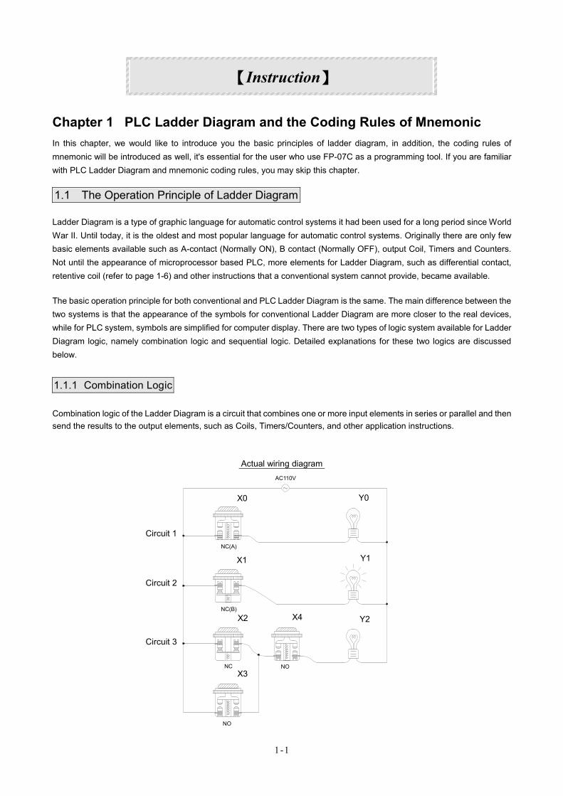
Combination logic of the Ladder Diagram is a circuit that combines one or more input elements in series or parallel and then send the results to the output elements, such as Coils, Timers/Counters, and other application instructions.
Actual wiring diagram
Circuit 1
Circuit 2
Circuit 3
NO
NC
X3
NC(B)
X2
NO(A)
X1
NO
X4 Y2
Y1
X0
AC110V
Y0
【Instruction】
AC110V
X0 Y0
X1 Y1
Y2X2 X4NC(B)
NC(A)
NO NC
NO
X3
1-2
Conventional Ladder Diagram PLC Ladder Diagram
circuit 1
circuit 2
circuit 3
X0
X1
X2
X3
X4
Y0
Y1
Y2
circuit 1
circuit 2
circuit 3
X0
X1
X2
X3
X4
Y0
Y1
Y2
The above example illustrated the combination logic using the actual wiring diagram, conventional Ladder Diagram, and PLC Ladder Diagram. Circuit 1 uses a NO (Normally Open) switch that is also called "A" switch or contact. Under normal condition (switch is not pressed), the switch contact is at OFF state and the light is off. If the switch is pressed, the contact status turns ON and the light is on. In contrast, circuit 2 uses a NC (Normally Close) switch that is also called "B" switch or contact. Under normal condition, the switch contact is at ON state and the light is on. If the switch is pressed, the contact status turns OFF and the light also turns off.
Circuit 3 contains more than one input element. Output Y2 light will turn on under the condition when X2 is closed or X3 switches to ON, and X4 must switch ON too.
1.1.2 Sequential Logic
The sequential logic is a circuit with feedback control; that is, the output of the circuit will be feedback as an input to the same circuit. The output result remains in the same state even if the input condition changes to the original position. This process can be best explained by the ON/OFF circuit of a latched motor driver as shown in below.
Actual wiring diagram
NO NC
X5
AC110V
X6
~
Y3START switch STOP switch
Relay
Contact 2
Contact 1
Motor
AC110V
X6
Contact 1
X5 Y3
Contact 2
Motor
Relay STOP switchSTART switch
NO NC
1-3
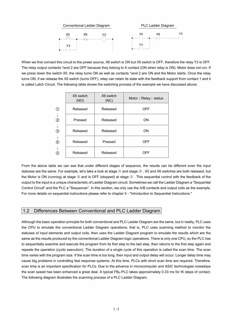
Conventional Ladder Diagram PLC Ladder Diagram
X5
Y3
X6 Y3
X5
Y3
X6 Y3
When we first connect this circuit to the power source, X6 switch is ON but X5 switch is OFF, therefore the relay Y3 is OFF. The relay output contacts 1and 2 are OFF because they belong to A contact (ON when relay is ON). Motor does not run. If we press down the switch X5, the relay turns ON as well as contacts 1and 2 are ON and the Motor starts. Once the relay turns ON, if we release the X5 switch (turns OFF), relay can retain its state with the feedback support from contact 1 and it is called Latch Circuit. The following table shows the switching process of the example we have discussed above.
X5 switch (NO)
X6 switch (NC) Motor(Relay)status
Released Released OFF
Pressed Released ON
Released Released ON
Released Pressed OFF
↓
↓
↓
↓
Released Released OFF
From the above table we can see that under different stages of sequence, the results can be different even the input statuses are the same. For example, let’s take a look at stage and stage , X5 and X6 switches are both released, but the Motor is ON (running) at stage and is OFF (stopped) at stage . This sequential control with the feedback of the output to the input is a unique characteristic of Ladder Diagram circuit. Sometimes we call the Ladder Diagram a "Sequential Control Circuit" and the PLC a "Sequencer”. In this section, we only use the A/B contacts and output coils as the example. For more details on sequential instructions please refer to chapter 5 - "Introduction to Sequential Instructions."
1.2 Differences Between Conventional and PLC Ladder Diagram
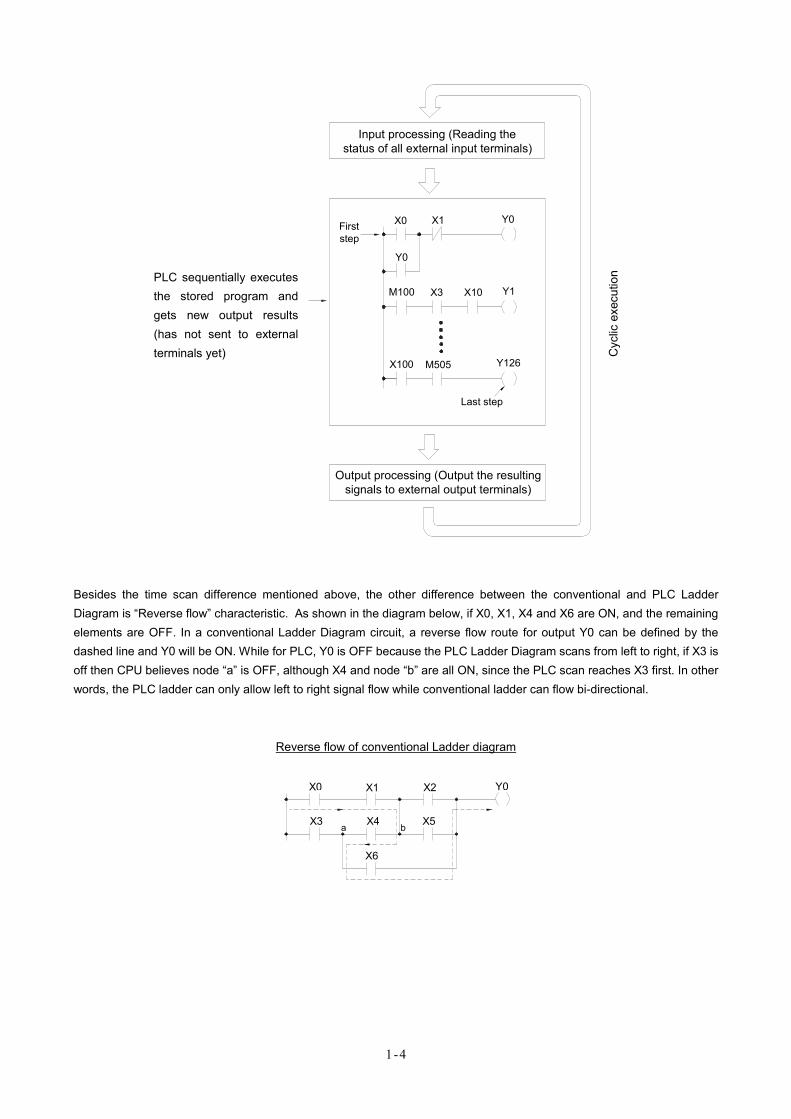
Although the basic operation principle for both conventional and PLC Ladder Diagram are the same, but in reality, PLC uses the CPU to emulate the conventional Ladder Diagram operations; that is, PLC uses scanning method to monitor the statuses of input elements and output coils, then uses the Ladder Diagram program to emulate the results which are the same as the results produced by the conventional Ladder Diagram logic operations. There is only one CPU, so the PLC has to sequentially examine and execute the program from its first step to the last step, then returns to the first step again and repeats the operation (cyclic execution). The duration of a single cycle of this operation is called the scan time. The scan time varies with the program size. If the scan time is too long, then input and output delay will occur. Longer delay time may cause big problems in controlling fast response systems. At this time, PLCs with short scan time are required. Therefore, scan time is an important specification for PLCs. Due to the advance in microcomputer and ASIC technologies nowadays the scan speed has been enhanced a great deal. A typical FBE-PLC takes approximately 0.33 ms for IK steps of contact. The following diagram illustrates the scanning process of a PLC Ladder Diagram.
1-4
PLC sequentially executes the stored program and gets new output results (has not sent to external terminals yet)
X0
Y0
M100
X100
X1
X3
M505
X10
Y126
Y0
Y1
Firststep
Last step
Input processing (Reading thestatus of all external input terminals)
Output processing (Output the resultingsignals to external output terminals)
Cyc
lic e
xecu
tion
Besides the time scan difference mentioned above, the other difference between the conventional and PLC Ladder Diagram is “Reverse flow” characteristic. As shown in the diagram below, if X0, X1, X4 and X6 are ON, and the remaining elements are OFF. In a conventional Ladder Diagram circuit, a reverse flow route for output Y0 can be defined by the dashed line and Y0 will be ON. While for PLC, Y0 is OFF because the PLC Ladder Diagram scans from left to right, if X3 is off then CPU believes node “a” is OFF, although X4 and node “b” are all ON, since the PLC scan reaches X3 first. In other words, the PLC ladder can only allow left to right signal flow while conventional ladder can flow bi-directional.
Reverse flow of conventional Ladder diagram
X2
X5
X0
X3
X1
X4
X6
a b
Y0
X1 Y0X2 X0
X3 X5X4
X6
a b
1-5
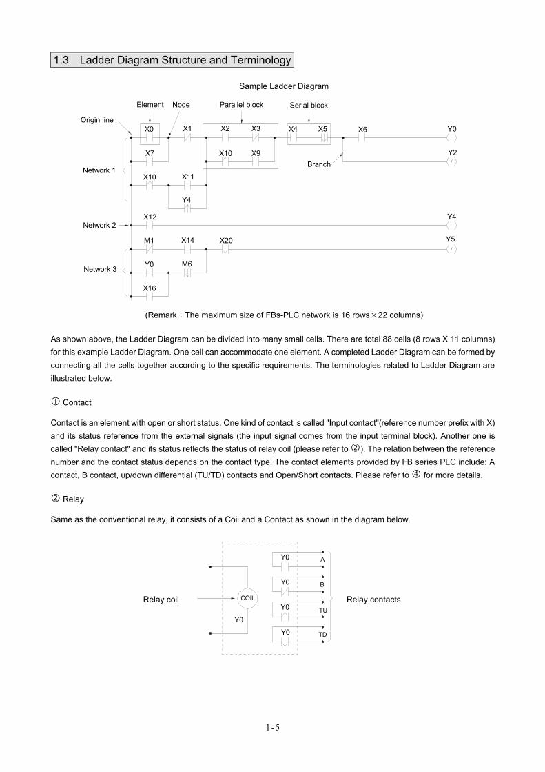
1.3 Ladder Diagram Structure and Terminology
Sample Ladder Diagram
Y4
X11
X14
M6Y0
X16
X10
X12
M1 X20
X1X0
X7 X10
X2
X9
X3 X4 X5 X6
/
Y4
Y5
/
Y2
Y0
Serial blockParallel blockNodeElement
Origin line
Network 1
Network 2
Network 3
Branch
(Remark:The maximum size of FBs-PLC network is 16 rows×22 columns)
As shown above, the Ladder Diagram can be divided into many small cells. There are total 88 cells (8 rows X 11 columns) for this example Ladder Diagram. One cell can accommodate one element. A completed Ladder Diagram can be formed by connecting all the cells together according to the specific requirements. The terminologies related to Ladder Diagram are illustrated below.
Contact
Contact is an element with open or short status. One kind of contact is called "Input contact"(reference number prefix with X) and its status reference from the external signals (the input signal comes from the input terminal block). Another one is called "Relay contact" and its status reflects the status of relay coil (please refer to ). The relation between the reference number and the contact status depends on the contact type. The contact elements provided by FB series PLC include: A contact, B contact, up/down differential (TU/TD) contacts and Open/Short contacts. Please refer to for more details.
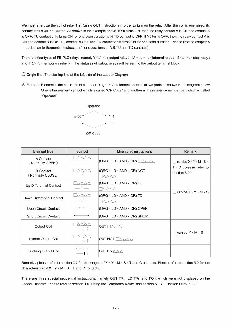
Relay
Same as the conventional relay, it consists of a Coil and a Contact as shown in the diagram below.
Relay coil
Y0
COIL
Y0
Y0
Y0
Y0
A
B
TU
TD
Relay contacts
Y5
X5X4 X6 Y0
Y2
Y4
X3X2
X9X10Branch
Serial blockParallel block
X1
X7
Y4
X10 X11
Origin line
Node Element
Network 1
X0
M6
M1
Y0
X12
X20
X16
Network 2
Network 3
X14
1-6
We must energize the coil of relay first (using OUT instruction) in order to turn on the relay. After the coil is energized, its contact status will be ON too. As shown in the example above, if Y0 turns ON, then the relay contact A is ON and contact B is OFF, TU contact only turns ON for one scan duration and TD contact is OFF. If Y0 turns OFF, then the relay contact A is ON and contact B is ON, TU contact is OFF and TD contact only turns ON for one scan duration (Please refer to chapter 5 “Introduction to Sequential Instructions” for operations of A,B,TU and TD contacts).
There are four types of FB-PLC relays, namely Y△△△(output relay), M△△△△(internal relay), S△△△(step relay)
and TR△△(temporary relay). The statuses of output relays will be sent to the output terminal block.
Origin-line: The starting line at the left side of the Ladder Diagram.
Element: Element is the basic unit of a Ladder Diagram. An element consists of two parts as shown in the diagram below. One is the element symbol which is called “OP Code” and another is the reference number part which is called “Operand”.
Operand
X100 Y15
OP Code
Element type Symbol Mnemonic instructions Remark
A Contact (Normally OPEN)
□△△△△
(ORG、LD、AND、OR) □△△△△
B Contact (Normally CLOSE)
□△△△△
(ORG、LD、AND、OR) NOT □△△△△
□ can be X、Y、M、S、
T、C(please refer to section 3.2)
Up Differential Contact □△△△△
(ORG、LD、AND、OR) TU □△△△△
Down Differential Contact □△△△△
(ORG、LD、AND、OR) TD □△△△△
□ can be X、Y、M、S
Open Circuit Contact (ORG、LD、AND、OR) OPEN
Short Circuit Contact (ORG、LD、AND、OR) SHORT
Output Coil □△△△△
OUT □△△△△
Inverse Output Coil □△△△△
OUT NOT □△△△△
□ can be Y、M、S
Latching Output Coil Y△△△
L OUT L Y△△△
Remark:please refer to section 3.2 for the ranges of X、Y、M、S、T and C contacts. Please refer to section 5.2 for the characteristics of X、Y、M、S、T and C contacts.
There are three special sequential instructions, namely OUT TRn, LD TRn and FOn, which were not displayed on the Ladder Diagram. Please refer to section 1.6 “Using the Temporary Relay” and section 5.1.4 “Function Output FO”.
1-7
Node: The connection point between two or more elements(please refer to section 5.3)
Block: a circuit consists of two or more elements. There are two basic types of blocks:
• Serial block:Two or more elements are connected in series to form a single row circuit.
Example:
• Parallel block: Parallel block is a type of a parallel closed circuit formed by connecting elements or serial blocks in parallel.
Example:
Remark: Complicated block can be formed by the combination of the single element, serial blocks and parallel blocks. When design a Ladder Diagram with mnemonic entry, it is necessary to break down the circuits into element, serial, and parallel blocks. Please refer to section 1.5.
Branch: In any network, branch is obtained if the right side of a vertical line is connected with two or more rows of circuits.
Example:
Branch
Merge line is defined as another vertical line at the right side of a branch line that merges the branch circuits into a closed circuit (forming a parallel block). This vertical line is called “Merge line”.
Branch line Merge line
If both the right and the left sides of the vertical line are connected with two or more rows of circuits, then it is both a branch line and a merge line as shown in the example below.
Example:
Parallel block 1 Parallel block 2
Block 1 merge line Block 2 branch line
1-8
Network: Network is a circuit representing a specified function. It consists of the elements, branches, and blocks. Network is the basic unit in the Ladder Diagram which is capable of executing the completed functions, and the program of Ladder Diagram is formed by connecting networks together. The beginning of the network is the origin line. If two circuits are connected by a vertical line, then they belong to the same network. If there is no vertical line between the two circuits, then they belong to two different networks. Figure 1, shows three (1~3) networks.
1.4 The Coding Rules of Mnemonic (Users of WinProladder can skip this section)
It’s very easy to program FB-PLC with WinProladder software package, just key-in the ladder symbols as they appear on your CRT screen directly to form a ladder diagram program. But for the users who are using FPC-07 to program FB-PLC they have to translate ladder diagram into mnemonic instructions by themselves. Since FPC-07 only can input program with mnemonic instruction, this section till section 1.6 will furnish you with the coding rules to translate ladder diagrams into mnemonic instructions.
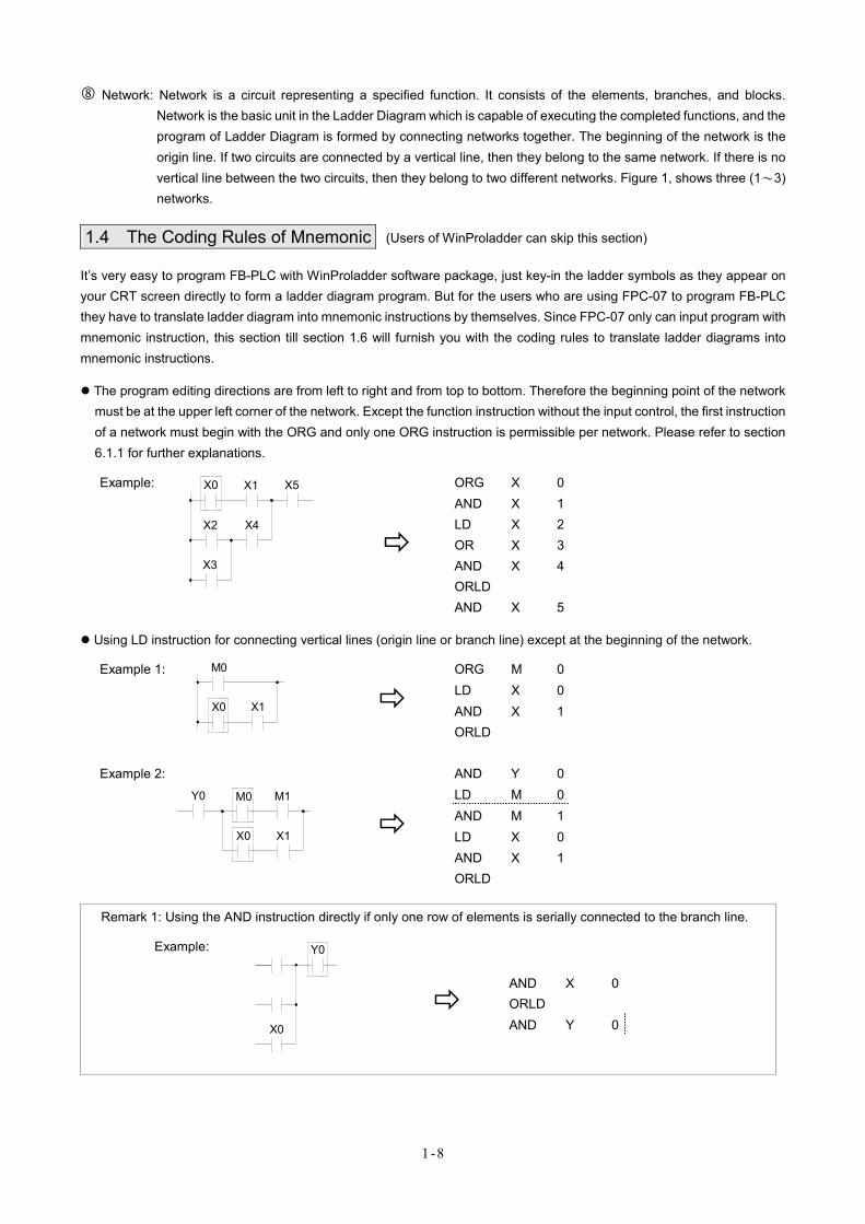
The program editing directions are from left to right and from top to bottom. Therefore the beginning point of the network must be at the upper left corner of the network. Except the function instruction without the input control, the first instruction of a network must begin with the ORG and only one ORG instruction is permissible per network. Please refer to section 6.1.1 for further explanations.
ORG X 0AND X 1LD X 2OR X 3AND X 4ORLD
Example: X0
X2
X3
X1
X4
X5
AND X 5
Using LD instruction for connecting vertical lines (origin line or branch line) except at the beginning of the network.
ORG M 0LD X 0AND X 1
Example 1:
X0
M0
X1
ORLD
AND Y 0LD M 0AND M 1LD X 0AND X 1
Example 2:
X0
M0
X1
M1Y0
ORLD
Remark 1: Using the AND instruction directly if only one row of elements is serially connected to the branch line.
AND X 0 ORLD AND Y 0
Example:
X0
Y0
1-9
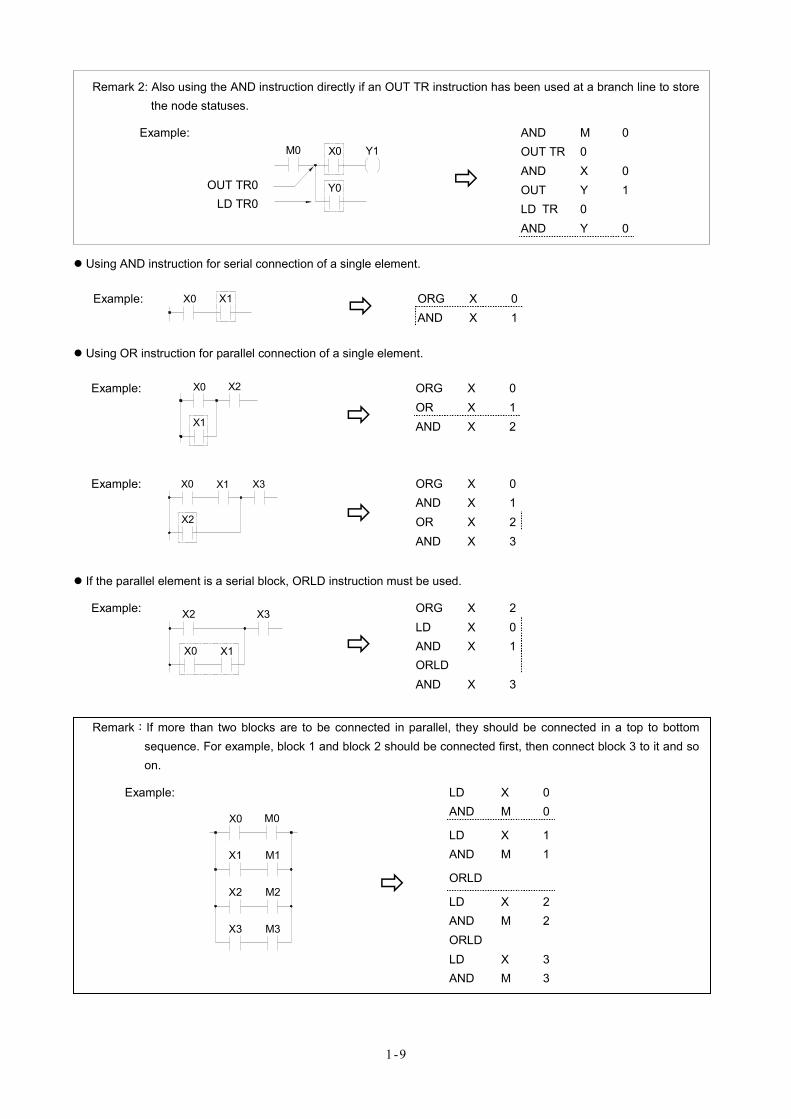
Remark 2: Also using the AND instruction directly if an OUT TR instruction has been used at a branch line to store the node statuses.
AND M 0 OUT TR 0 AND X 0 OUT Y 1 LD TR 0
Example:
OUT TR0 LD TR0
Y0
X0 Y1M0
AND Y 0
Using AND instruction for serial connection of a single element.
ORG X 0Example: X0 X1
AND X 1
Using OR instruction for parallel connection of a single element.
ORG X 0OR X 1AND X 2
Example: X0 X2
X1
ORG X 0AND X 1OR X 2
Example: X0 X1 X3
X2
AND X 3
If the parallel element is a serial block, ORLD instruction must be used.
ORG X 2LD X 0AND X 1ORLD
Example: X3X2
X1X0
AND X 3
Remark:If more than two blocks are to be connected in parallel, they should be connected in a top to bottom sequence. For example, block 1 and block 2 should be connected first, then connect block 3 to it and so on.
LD X 0AND M 0
LD X 1AND M 1
ORLD
LD X 2AND M 2ORLD LD X 3
Example:
X0 M0
X1
X2
X3
M1
M2
M3
AND M 3
1-10
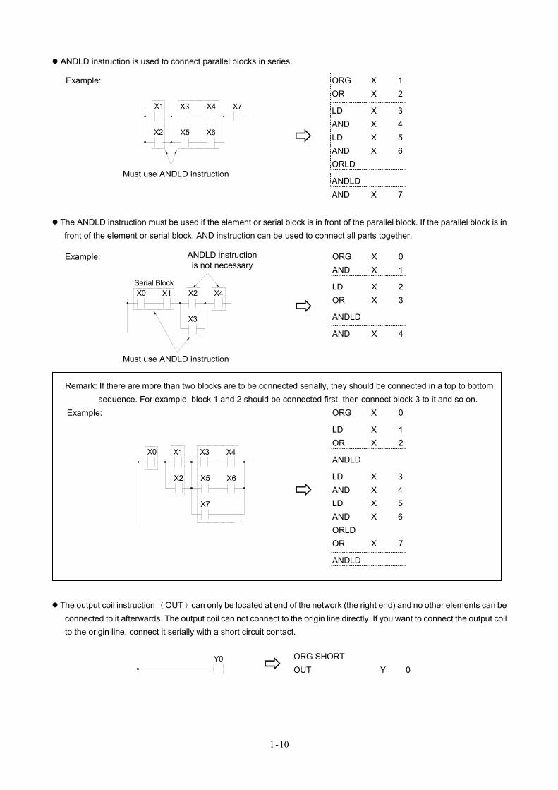
ANDLD instruction is used to connect parallel blocks in series.
ORG X 1 OR X 2
LD X 3 AND X 4 LD X 5 AND X 6 ORLD
ANDLD
Example:
X1
X2
X3
X5 X6
X7X4
Must use ANDLD instruction
AND X 7
The ANDLD instruction must be used if the element or serial block is in front of the parallel block. If the parallel block is in front of the element or serial block, AND instruction can be used to connect all parts together.
ORG X 0 AND X 1
LD X 2 OR X 3
ANDLD
AND X 4
Example: ANDLD instruction is not necessary
X0 X1
X3
X2 X4Serial Block
Must use ANDLD instruction
Remark: If there are more than two blocks are to be connected serially, they should be connected in a top to bottom
sequence. For example, block 1 and 2 should be connected first, then connect block 3 to it and so on. ORG X 0
LD X 1 OR X 2
ANDLD
LD X 3 AND X 4 LD X 5 AND X 6 ORLD OR X 7
ANDLD
Example:
X6X5X2
X0 X1 X3
X7
X4
The output coil instruction (OUT)can only be located at end of the network (the right end) and no other elements can be connected to it afterwards. The output coil can not connect to the origin line directly. If you want to connect the output coil to the origin line, connect it serially with a short circuit contact.
ORG SHORT Y0
OUT Y 0
1-11
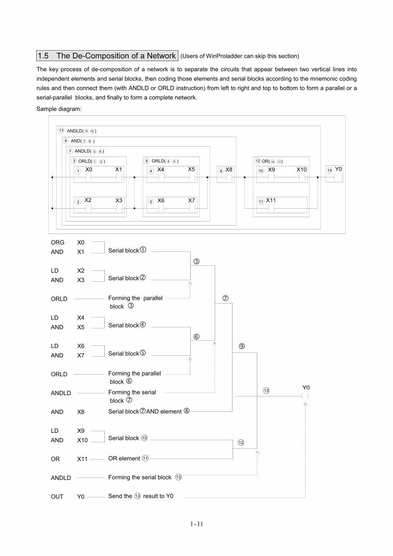
1.5 The De-Composition of a Network (Users of WinProladder can skip this section)
The key process of de-composition of a network is to separate the circuits that appear between two vertical lines into independent elements and serial blocks, then coding those elements and serial blocks according to the mnemonic coding rules and then connect them (with ANDLD or ORLD instruction) from left to right and top to bottom to form a parallel or a serial-parallel blocks, and finally to form a complete network.
Sample diagram:
8
6
4
5
13
9
7
3
1
2
1410
12
11
9
7 8
1
3 6
2 4 5 10 11
ANDLD( )
AND( )
ANDLD( )
ORLD( )
X0 X1
X2 X3
ORLD( )
X4 X5
X6 X7
X8 X9
X11
X10 Y0OR( )
12
ORG AND
X0 X1
Serial block
LD AND
X2 X3
Serial block
ORLD
Forming the parallel block
LD AND
X4 X5
Serial block
LD AND
X6 X7
Serial block
ORLD
Forming the parallel block
ANDLD
Forming the serial block
AND
X8
Serial block AND element
Y0
LD AND
X9 X10
Serial block ○10
○12
OR
X11
OR element ○11
ANDLD
Forming the serial block ○13
OUT Y0 Send the ○13 result to Y0
○13 Y0
1-12
1.6 Using Temporary Relays (Users of WinProladder can skip this section)
The network de-composition method for mnemonic coding demonstrated in section 1.5 does not apply to the branched circuit or branched block. In order to input the program using the method shown in section 1.5, It must first to store the statuses of branched nodes in temporary relays. The program design should avoid having branched circuit or branched block as much as possible. Please refer the next section “Program Simplification Techniques”. Two situations that must use the TR are described at below.
Branched circuit: Merge line does not exist at the right side of the branch line or there is a merge line at the right side of the branch line but they are not in the same row.
Example: * indicates setting of TR relay Without merge line
Although this branch has merge lines but they are not in the same row, so this is also a branched circuit
Branched block:The horizontal parallel blocks with a branch in one of the blocks.
Example: Merge line
Branch line
Remark 1: The OUT TR instruction must be programmed at the top of the branched point. LD TRn instruction is used at the starting point of the circuits after second rows of the branch line for regaining the branch line status before you can connect any element to the circuits. AND instruction must be used to connect the first element after OUT TRn or LD TRn instruction. LD instruction is not allowed in this case.
Remark 2: A network can have up to 40 TR points and the TR number can not be used repeatedly in the same network. It is recommended to use the numbers 1,2,3… with sequence. The TR number must be the same in the same branch line. For example, if a branch line uses OUT TR0, then starting from row 2, LD TR0 must be used for connection.
Remark 3: If the branch line of a branched circuit or a branched block is the origin line, then ORG or LD instructions can be used directly and TR contact is not necessary.
Remark 4: If any one of the branched circuit rows is not connected to the output coil (there are serially connected elements in between), and other circuits also exist after the second row, a TR instruction must be used at the branch points.
1-13
AND X 0 OUT TR 0 AND X 1 OUT Y 0 LD TR 0 ←─ Begins from row 2AND X 2 OUT Y 1 LD TR 0 ←─ Begins from row 3
Example:
X0 X1
X2
Y0OUT TR0
Y1
Y2LD TR0
OUT Y 2
ORG X 1 AND X 2 LD X 3 OUT TR 0 AND X 4 ORLD OUT TR 1 AND X 5AND X 6
←─ Uses AND Instruction after TR instruction
LD TR 1 AND X 7
←─ Uses LD TR instruction to return to TR branch line
LD TR 0 AND X 9ORLD
←─ Uses AND instruction after TR instruction
AND X 8 ORLD
Example:
X1
X3
Y0
OUT TR1
LD TR0
X2
X4
X5
X7
X6
X8
X9OUT TR0
block 1 block 2
LD TR1
block 3
OUT Y 0
The above sample diagram shows a typical example of connecting two parallel blocks in series. Block 3 is formed when the element X9 is introduced into the network and the two parallel blocks become the branched blocks.
TR instruction is not necessary because the(*)point is the origin line.
If have already used TR relay to connect two blocks serially, then ANDLD instruction is not necessary.
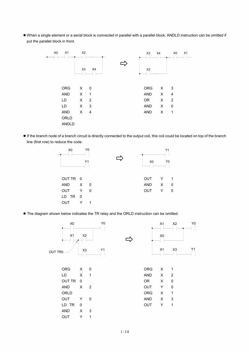
1.7 Program Simplification Techniques
If a single element is connected in parallel to a serial block, The ORLD instruction can be omitted if the serial block is connected on top of this single element.
X0
X1 X2
X1 X2
X0
LD X 0 LD X 1LD X 1 AND X 2AND X 2 OR X 0ORLD
*
1-14
When a single element or a serial block is connected in parallel with a parallel block, ANDLD instruction can be omitted if put the parallel block in front.
X0 X2X1
X3 X4
X2
X0 X1X3 X4
ORG X 0 ORG X 3AND X 1 AND X 4LD X 2 OR X 2LD X 3
AND X 0AND X 4 AND X 1ORLD ANDLD
If the branch node of a branch circuit is directly connected to the output coil, this coil could be located on top of the branch line (first row) to reduce the code.
Y0
Y1
X0
X0 Y0
Y1
OUT TR 0 OUT Y 1AND X 0 AND X 0OUT Y 0 OUT Y 0LD TR 0
OUT Y 1
The diagram shown below indicates the TR relay and the ORLD instruction can be omitted.
X0 Y0
Y1OUT TR0
X1 X2
X3
Y0
X0
Y1
X1 X2
X1 X3
ORG X 0 ORG X 1LD X 1 AND X 2OUT TR 0 OR X 0AND X 2
OUT Y 0ORLD ORG X 1OUT Y 0 AND X 3LD TR 0 OUT Y 1AND X 3 OUT Y 1
1-15
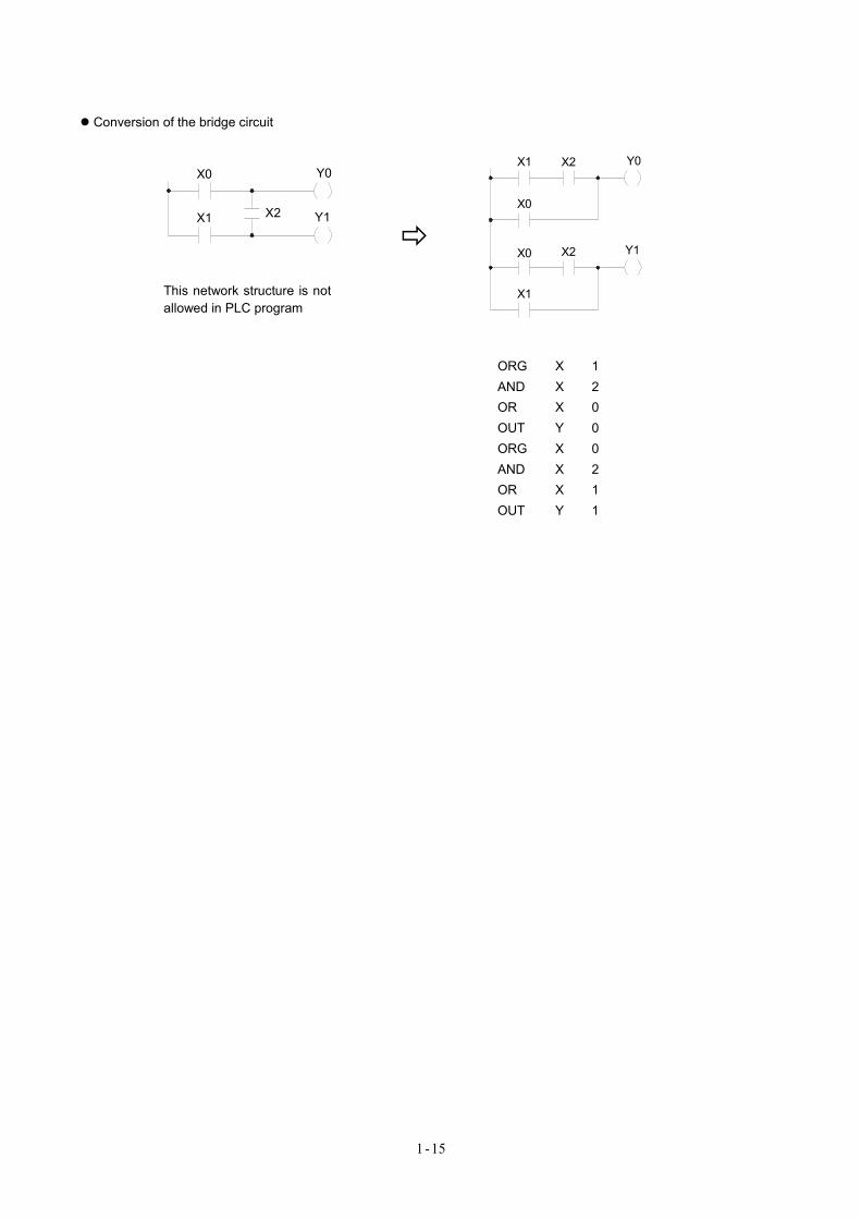
Conversion of the bridge circuit
X0 Y0
Y1X1 X2
This network structure is not allowed in PLC program
X1 Y0
Y1
X0
X2
X2
X1
X0
ORG X 1 AND X 2 OR X 0
OUT Y 0 ORG X 0 AND X 2 OR X 1 OUT Y 1

MEMO
2-1
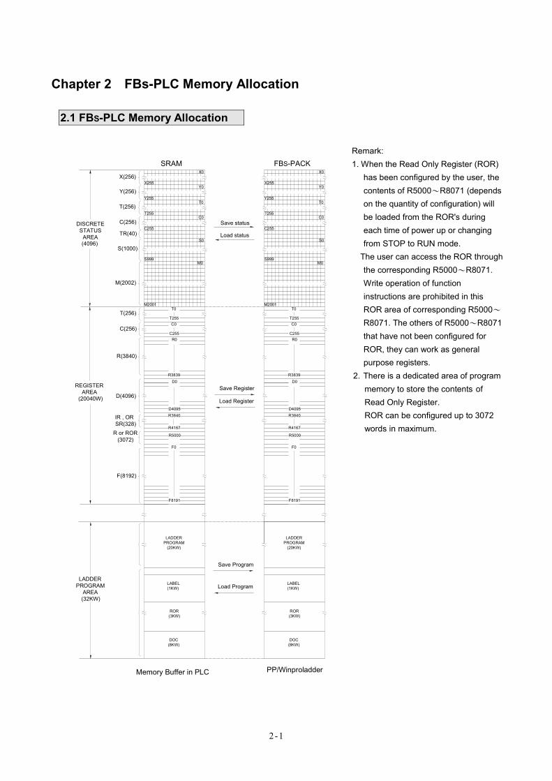
Chapter 2 FBs-PLC Memory Allocation
Y(256)
X(256)
T(256)
C(256)
TR(40)
S(1000)
M(2002)
DISCRETESTATUS
AREA(4096)
T(256)
C(256)
R(3840)
D(4096)
IR , ORSR(328)
R or ROR(3072)
LADDERPROGRAM
AREA(32KW)
Memory Buffer in PLC PP/Winproladder
X0
Y0X255
T255
T0
C0
C255
S0
S999M0
M2001T0
T255C0
C255R0
D0
D4095R3840
R4167
R5000
F0
F8191
DOC(8KW)
ROR(3KW)
LADDERPROGRAM
(20KW)
LABEL(1KW)
REGISTERAREA
(20040W)
Save Register
Load Register
Save Program
Load Program
SRAM
R3839
F(8192)
Save status
Load status
FBS-PACKX0
Y0X255
T255
T0
C0
C255
S0
S999M0
M2001T0
T255C0
C255R0
D0
D4095R3840
R4167
R5000
F0
F8191
DOC(8KW)
ROR(3KW)
LADDERPROGRAM
(20KW)
LABEL(1KW)
R3839
Y255Y255
2.1 FBS-PLC Memory Allocation
Remark: 1. When the Read Only Register (ROR)
has been configured by the user, the contents of R5000~R8071 (depends on the quantity of configuration) will be loaded from the ROR's during each time of power up or changing from STOP to RUN mode.
The user can access the ROR through the corresponding R5000~R8071. Write operation of function instructions are prohibited in this ROR area of corresponding R5000~
R8071. The others of R5000~R8071 that have not been configured for ROR, they can work as general purpose registers.
2. There is a dedicated area of program memory to store the contents of Read Only Register. ROR can be configured up to 3072 words in maximum.
2-2
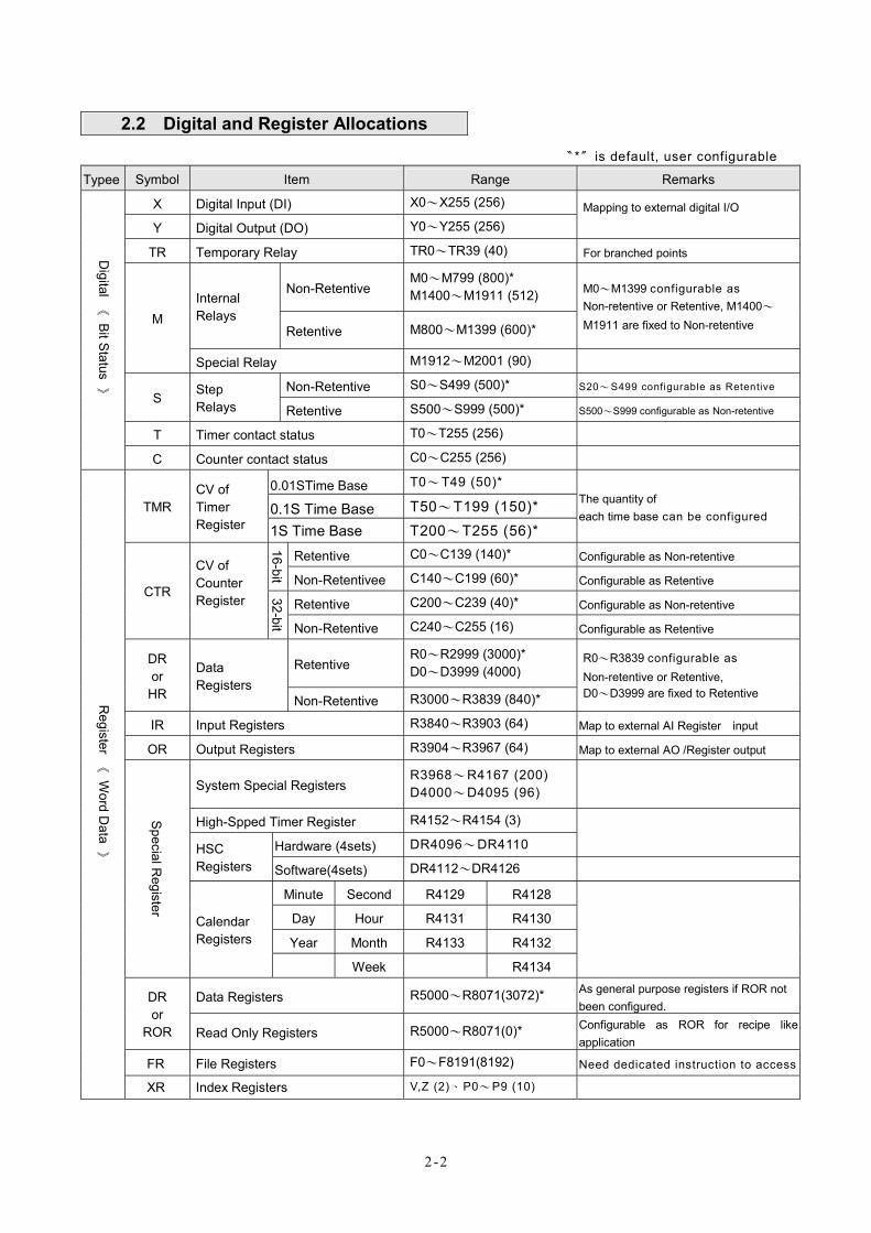
2.2 Digital and Register Allocations 〝*〞 is default, user configurable
Typee Symbol Item Range Remarks
X Digital Input (DI) X0~X255 (256)
Y Digital Output (DO) Y0~Y255 (256) Mapping to external digital I/O
TR Temporary Relay TR0~TR39 (40) For branched points
Non-Retentive M0~M799 (800)* M1400~M1911 (512) Internal
Relays Retentive M800~M1399 (600)*
M0~M1399 configurable as Non-retentive or Retentive, M1400~
M1911 are fixed to Non-retentive M
Special Relay M1912~M2001 (90)
Non-Retentive S0~S499 (500)* S20~ S499 configurable as Retentive S
Step Relays Retentive S500~S999 (500)* S500~S999 configurable as Non-retentive
T Timer contact status T0~T255 (256)
Digital
《 B
it Status
》
C Counter contact status C0~C255 (256)
0.01STime Base T0~T49 (50)*
0.1S Time Base T50~T199 (150)* TMR CV of Timer Register 1S Time Base T200~T255 (56)*
The quantity of each time base can be configured
Retentive C0~C139 (140)* Configurable as Non-retentive
16-bit Non-Retentivee C140~C199 (60)* Configurable as Retentive
Retentive C200~C239 (40)* Configurable as Non-retentive CTR
CV of Counter Register
32-bit Non-Retentive C240~C255 (16) Configurable as Retentive
Retentive R0~R2999 (3000)* D0~D3999 (4000)
DR or
HR
Data Registers
Non-Retentive R3000~R3839 (840)*
R0~R3839 configurable as Non-retentive or Retentive, D0~D3999 are fixed to Retentive
IR Input Registers R3840~R3903 (64) Map to external AI Register input
OR Output Registers R3904~R3967 (64) Map to external AO /Register output
System Special Registers R3968~R4167 (200) D4000~D4095 (96)
High-Spped Timer Register R4152~R4154 (3)
Hardware (4sets) DR4096~DR4110
HSC Registers Software(4sets) DR4112~DR4126
Minute Second R4129 R4128
Day Hour R4131 R4130
Year Month R4133 R4132
Special R
egister
Calendar Registers
Week R4134
Data Registers R5000~R8071(3072)* As general purpose registers if ROR not been configured.
DR or
ROR Read Only Registers R5000~R8071(0)* Configurable as ROR for recipe like application
FR File Registers F0~F8191(8192) Need dedicated instruction to access
Register
《 W
ord Data
》
XR Index Registers V,Z (2)、P0~P9 (10)
2-3
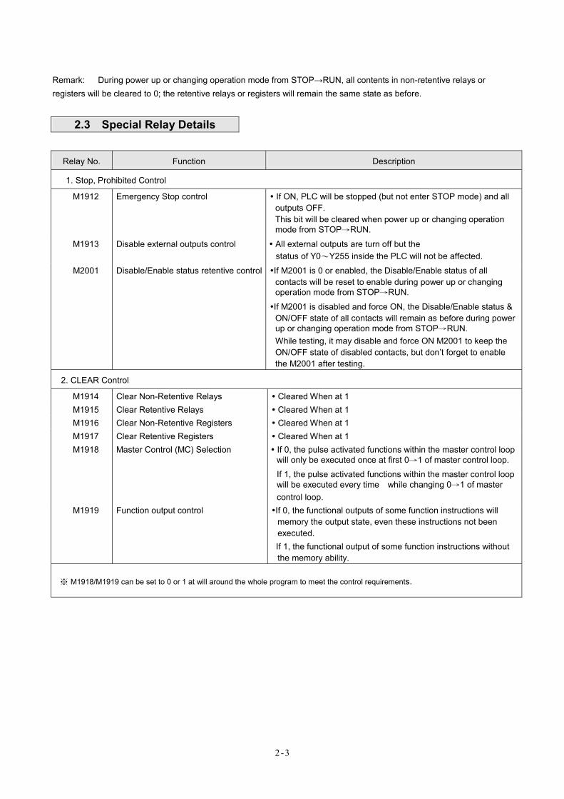
Remark: During power up or changing operation mode from STOP→RUN, all contents in non-retentive relays or registers will be cleared to 0; the retentive relays or registers will remain the same state as before.
Relay No. Function Description
1. Stop, Prohibited Control
M1912 Emergency Stop control If ON, PLC will be stopped (but not enter STOP mode) and all outputs OFF. This bit will be cleared when power up or changing operation mode from STOP→RUN.
M1913 Disable external outputs control All external outputs are turn off but the status of Y0~Y255 inside the PLC will not be affected.
M2001 Disable/Enable status retentive control If M2001 is 0 or enabled, the Disable/Enable status of all contacts will be reset to enable during power up or changing operation mode from STOP→RUN.
If M2001 is disabled and force ON, the Disable/Enable status & ON/OFF state of all contacts will remain as before during power up or changing operation mode from STOP→RUN. While testing, it may disable and force ON M2001 to keep the ON/OFF state of disabled contacts, but don’t forget to enable the M2001 after testing.
2. CLEAR Control
M1914 Clear Non-Retentive Relays Cleared When at 1 M1915 Clear Retentive Relays Cleared When at 1 M1916 Clear Non-Retentive Registers Cleared When at 1 M1917 Clear Retentive Registers Cleared When at 1 M1918 Master Control (MC) Selection If 0, the pulse activated functions within the master control loop
will only be executed once at first 0→1 of master control loop.
If 1, the pulse activated functions within the master control loop will be executed every time while changing 0→1 of master control loop.
M1919 Function output control If 0, the functional outputs of some function instructions will memory the output state, even these instructions not been executed.
If 1, the functional output of some function instructions without the memory ability.
※ M1918/M1919 can be set to 0 or 1 at will around the whole program to meet the control requirements.
2.3 Special Relay Details
2-4
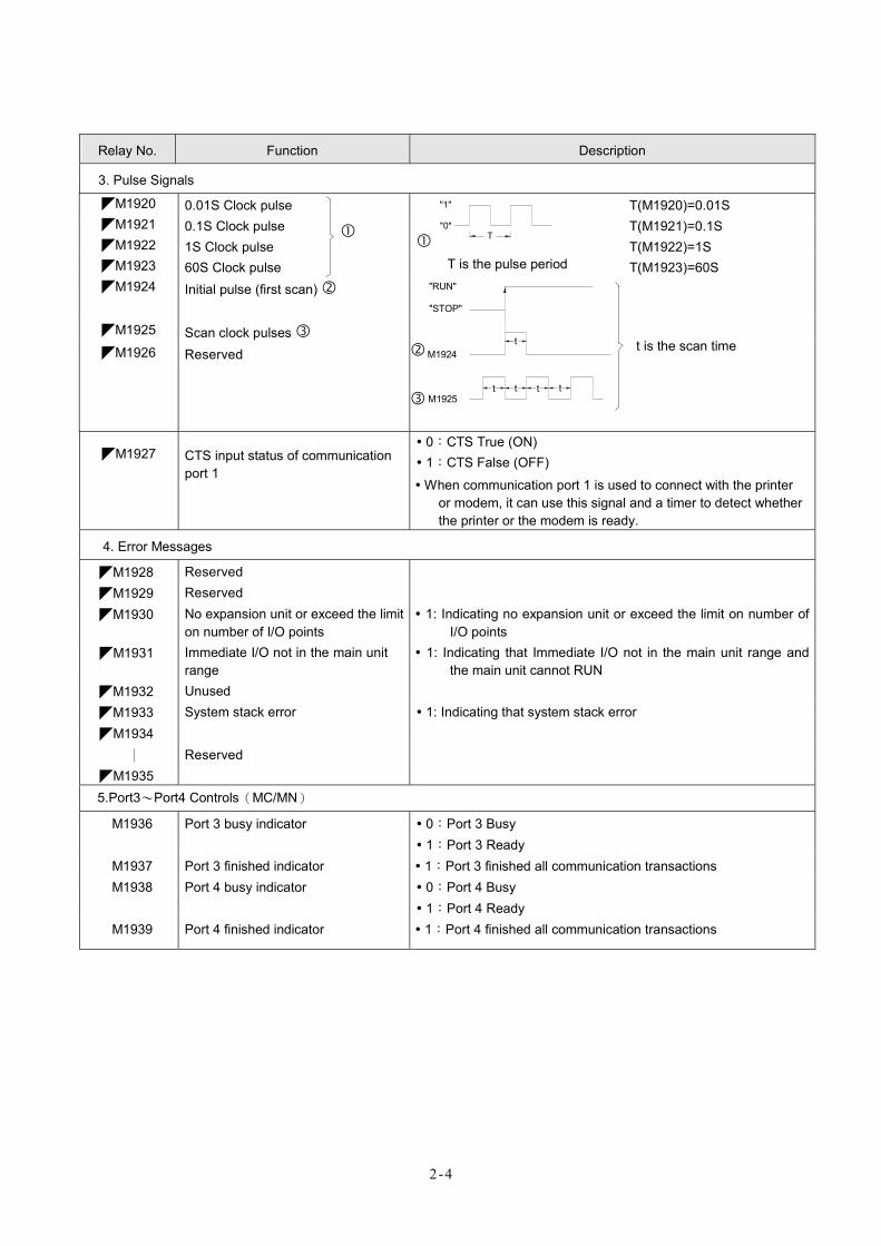
Relay No. Function Description
3. Pulse Signals
◤M1920 0.01S Clock pulse T(M1920)=0.01S ◤M1921 0.1S Clock pulse T(M1921)=0.1S ◤M1922 1S Clock pulse T(M1922)=1S ◤M1923 60S Clock pulse
"1"
"0"T
T is the pulse period T(M1923)=60S ◤M1924 Initial pulse (first scan)
◤M1925 Scan clock pulses ◤M1926 Reserved
M1925
M1924
"STOP"
"RUN"
t
t t t t
t is the scan time
◤M1927 CTS input status of communication port 1
0:CTS True (ON) 1:CTS False (OFF)
When communication port 1 is used to connect with the printer or modem, it can use this signal and a timer to detect whether the printer or the modem is ready.
4. Error Messages
◤M1928 Reserved ◤M1929 Reserved ◤M1930 No expansion unit or exceed the limit
on number of I/O points 1: Indicating no expansion unit or exceed the limit on number of
I/O points ◤M1931 Immediate I/O not in the main unit
range 1: Indicating that Immediate I/O not in the main unit range and
the main unit cannot RUN ◤M1932 Unused ◤M1933 System stack error 1: Indicating that system stack error ◤M1934
│ Reserved ◤M1935 5.Port3~Port4 Controls(MC/MN)
M1936 Port 3 busy indicator 0:Port 3 Busy 1:Port 3 Ready
M1937 Port 3 finished indicator 1:Port 3 finished all communication transactions M1938 Port 4 busy indicator 0:Port 4 Busy
1:Port 4 Ready M1939 Port 4 finished indicator 1:Port 4 finished all communication transactions
2-5
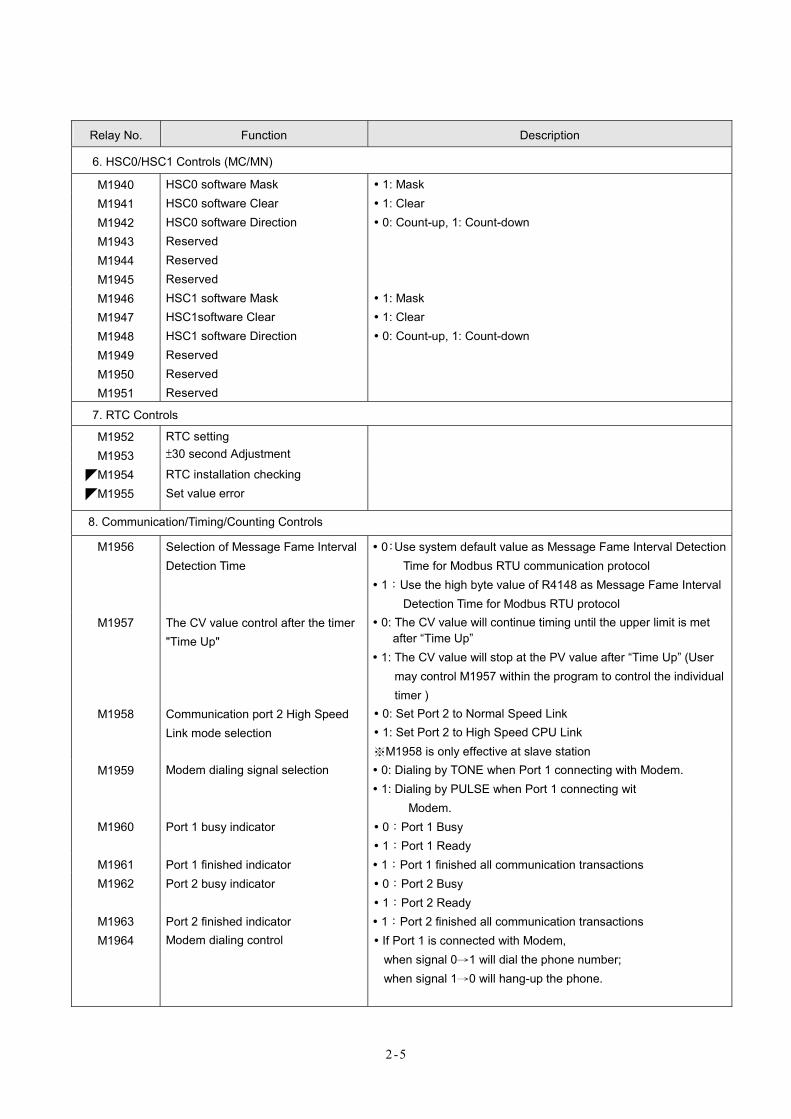
Relay No. Function Description
6. HSC0/HSC1 Controls (MC/MN)
M1940 HSC0 software Mask 1: Mask M1941 HSC0 software Clear 1: Clear M1942 HSC0 software Direction 0: Count-up, 1: Count-down M1943 Reserved M1944 Reserved M1945 Reserved M1946 HSC1 software Mask 1: Mask M1947 HSC1software Clear 1: Clear M1948 HSC1 software Direction 0: Count-up, 1: Count-down M1949 Reserved M1950 Reserved M1951 Reserved
7. RTC Controls
M1952 RTC setting M1953 ±30 second Adjustment
◤M1954 RTC installation checking ◤M1955 Set value error
8. Communication/Timing/Counting Controls
M1956 Selection of Message Fame Interval Detection Time
0:Use system default value as Message Fame Interval Detection Time for Modbus RTU communication protocol
1:Use the high byte value of R4148 as Message Fame Interval Detection Time for Modbus RTU protocol
M1957 The CV value control after the timer "Time Up"
0: The CV value will continue timing until the upper limit is met after “Time Up”
1: The CV value will stop at the PV value after “Time Up” (User may control M1957 within the program to control the individual timer )
M1958 Communication port 2 High Speed Link mode selection
0: Set Port 2 to Normal Speed Link 1: Set Port 2 to High Speed CPU Link
※M1958 is only effective at slave station M1959 Modem dialing signal selection 0: Dialing by TONE when Port 1 connecting with Modem.
1: Dialing by PULSE when Port 1 connecting wit Modem.
M1960 Port 1 busy indicator 0:Port 1 Busy 1:Port 1 Ready
M1961 Port 1 finished indicator 1:Port 1 finished all communication transactions M1962 Port 2 busy indicator 0:Port 2 Busy
1:Port 2 Ready M1963 M1964
Port 2 finished indicator Modem dialing control
1:Port 2 finished all communication transactions If Port 1 is connected with Modem, when signal 0→1 will dial the phone number; when signal 1→0 will hang-up the phone.
2-6
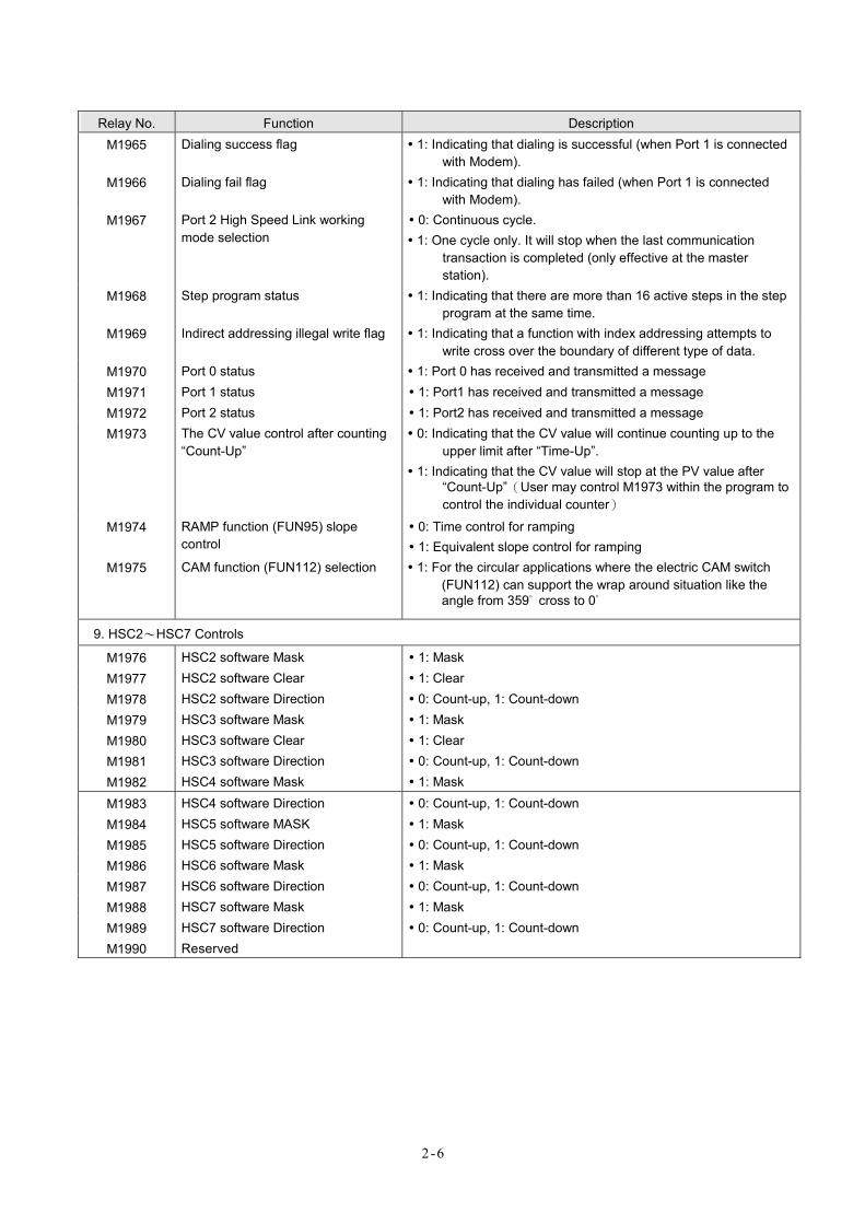
Relay No. Function Description M1965 Dialing success flag 1: Indicating that dialing is successful (when Port 1 is connected
with Modem). M1966 Dialing fail flag 1: Indicating that dialing has failed (when Port 1 is connected
with Modem). M1967 Port 2 High Speed Link working
mode selection 0: Continuous cycle. 1: One cycle only. It will stop when the last communication
transaction is completed (only effective at the master station).
M1968 Step program status 1: Indicating that there are more than 16 active steps in the step program at the same time.
M1969 Indirect addressing illegal write flag 1: Indicating that a function with index addressing attempts to write cross over the boundary of different type of data.
M1970 Port 0 status 1: Port 0 has received and transmitted a message M1971 Port 1 status 1: Port1 has received and transmitted a message M1972 Port 2 status 1: Port2 has received and transmitted a message M1973 The CV value control after counting
“Count-Up” 0: Indicating that the CV value will continue counting up to the
upper limit after “Time-Up”. 1: Indicating that the CV value will stop at the PV value after
“Count-Up”(User may control M1973 within the program to control the individual counter)
M1974 RAMP function (FUN95) slope control
0: Time control for ramping 1: Equivalent slope control for ramping
M1975 CAM function (FUN112) selection 1: For the circular applications where the electric CAM switch (FUN112) can support the wrap around situation like the angle from 359° cross to 0°
9. HSC2~HSC7 Controls
M1976 HSC2 software Mask 1: Mask M1977 HSC2 software Clear 1: Clear M1978 HSC2 software Direction 0: Count-up, 1: Count-down M1979 HSC3 software Mask 1: Mask M1980 HSC3 software Clear 1: Clear M1981 HSC3 software Direction 0: Count-up, 1: Count-down M1982 HSC4 software Mask 1: Mask
M1983 HSC4 software Direction 0: Count-up, 1: Count-down M1984 HSC5 software MASK 1: Mask M1985 HSC5 software Direction 0: Count-up, 1: Count-down M1986 HSC6 software Mask 1: Mask M1987 HSC6 software Direction 0: Count-up, 1: Count-down M1988 HSC7 software Mask 1: Mask
HSC7 software Direction 0: Count-up, 1: Count-down M1989 M1990 Reserved
2-7
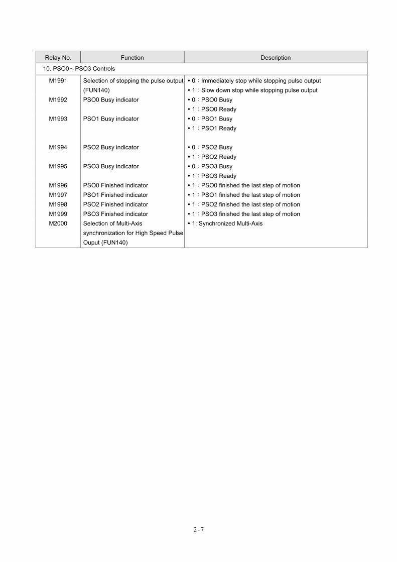
Relay No. Function Description
10. PSO0~PSO3 Controls
M1991 Selection of stopping the pulse output (FUN140)
0:Immediately stop while stopping pulse output 1:Slow down stop while stopping pulse output
M1992 PSO0 Busy indicator 0:PSO0 Busy 1:PSO0 Ready
M1993 PSO1 Busy indicator 0:PSO1 Busy 1:PSO1 Ready
M1994 PSO2 Busy indicator 0:PSO2 Busy 1:PSO2 Ready
M1995 PSO3 Busy indicator 0:PSO3 Busy 1:PSO3 Ready
M1996 PSO0 Finished indicator 1:PSO0 finished the last step of motion M1997 PSO1 Finished indicator 1:PSO1 finished the last step of motion M1998 PSO2 Finished indicator 1:PSO2 finished the last step of motion M1999 PSO3 Finished indicator 1:PSO3 finished the last step of motion M2000 Selection of Multi-Axis
synchronization for High Speed Pulse Ouput (FUN140)
1: Synchronized Multi-Axis
2-8
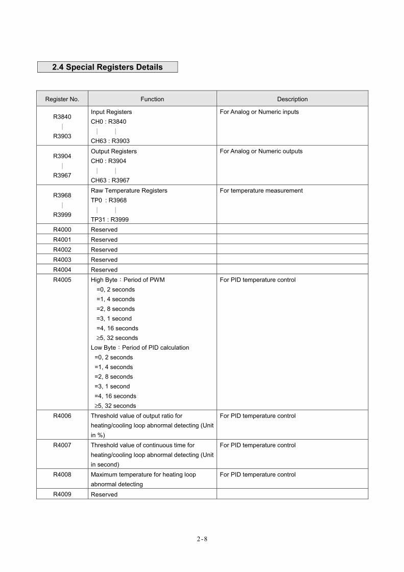
2.4 Special Registers Details
Register No. Function Description
R3840 │
R3903
Input Registers CH0 : R3840 │ │ CH63 : R3903
For Analog or Numeric inputs
R3904 │
R3967
Output Registers CH0 : R3904 │ │ CH63 : R3967
For Analog or Numeric outputs
R3968 │
R3999
Raw Temperature Registers TP0 : R3968 │ │ TP31 : R3999
For temperature measurement
R4000 Reserved R4001 Reserved R4002 Reserved R4003 Reserved R4004 Reserved R4005 High Byte:Period of PWM
=0, 2 seconds =1, 4 seconds =2, 8 seconds =3, 1 second =4, 16 seconds ≥5, 32 seconds
Low Byte:Period of PID calculation =0, 2 seconds =1, 4 seconds =2, 8 seconds =3, 1 second =4, 16 seconds ≥5, 32 seconds
For PID temperature control
R4006 Threshold value of output ratio for heating/cooling loop abnormal detecting (Unit in %)
For PID temperature control
R4007 Threshold value of continuous time for heating/cooling loop abnormal detecting (Unit in second)
For PID temperature control
R4008 Maximum temperature for heating loop abnormal detecting
For PID temperature control
R4009 Reserved
2-9
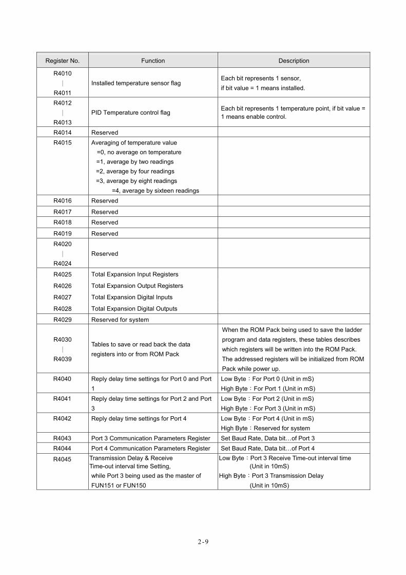
Register No. Function Description
R4010 │
R4011 Installed temperature sensor flag
Each bit represents 1 sensor, if bit value = 1 means installed.
R4012 │
R4013 PID Temperature control flag
Each bit represents 1 temperature point, if bit value = 1 means enable control.
R4014 Reserved R4015 Averaging of temperature value
=0, no average on temperature =1, average by two readings =2, average by four readings =3, average by eight readings
=4, average by sixteen readings
R4016 Reserved
R4017 Reserved
R4018 Reserved
R4019 Reserved
R4020 │
R4024 Reserved
R4025 Total Expansion Input Registers
R4026 Total Expansion Output Registers
R4027 Total Expansion Digital Inputs
R4028 Total Expansion Digital Outputs
R4029 Reserved for system
R4030 │
R4039
Tables to save or read back the data registers into or from ROM Pack
When the ROM Pack being used to save the ladder program and data registers, these tables describes which registers will be written into the ROM Pack. The addressed registers will be initialized from ROM Pack while power up.
R4040 Reply delay time settings for Port 0 and Port 1
Low Byte:For Port 0 (Unit in mS) High Byte:For Port 1 (Unit in mS)
R4041 Reply delay time settings for Port 2 and Port 3
Low Byte:For Port 2 (Unit in mS) High Byte:For Port 3 (Unit in mS)
R4042 Reply delay time settings for Port 4 Low Byte:For Port 4 (Unit in mS) High Byte:Reserved for system
R4043 Port 3 Communication Parameters Register Set Baud Rate, Data bit…of Port 3 R4044 Port 4 Communication Parameters Register Set Baud Rate, Data bit…of Port 4
R4045 Transmission Delay & Receive Time-out interval time Setting, while Port 3 being used as the master of FUN151 or FUN150
Low Byte:Port 3 Receive Time-out interval time (Unit in 10mS)
High Byte:Port 3 Transmission Delay (Unit in 10mS)
2-10
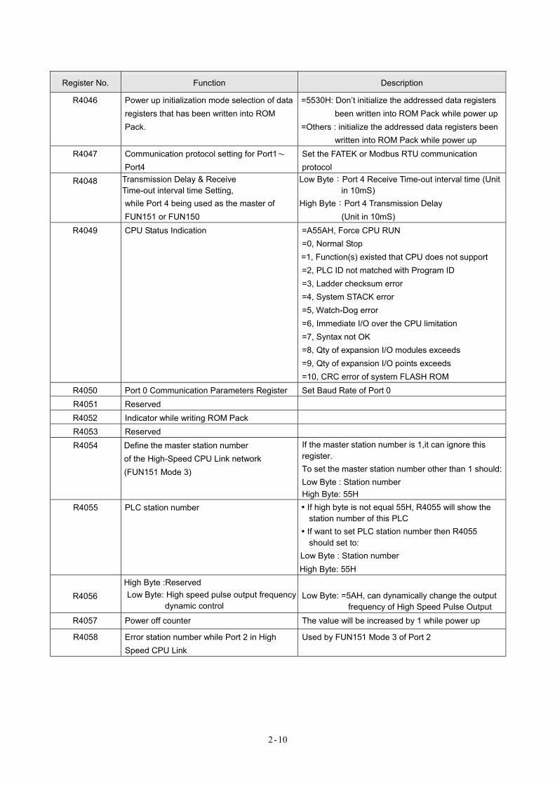
Register No. Function Description
R4046 Power up initialization mode selection of data registers that has been written into ROM Pack.
=5530H: Don’t initialize the addressed data registers been written into ROM Pack while power up
=Others : initialize the addressed data registers been written into ROM Pack while power up
R4047 Communication protocol setting for Port1~
Port4 Set the FATEK or Modbus RTU communication protocol
R4048 Transmission Delay & Receive Time-out interval time Setting, while Port 4 being used as the master of FUN151 or FUN150
Low Byte:Port 4 Receive Time-out interval time (Unit in 10mS)
High Byte:Port 4 Transmission Delay (Unit in 10mS)
R4049 CPU Status Indication =A55AH, Force CPU RUN =0, Normal Stop =1, Function(s) existed that CPU does not support =2, PLC ID not matched with Program ID =3, Ladder checksum error =4, System STACK error =5, Watch-Dog error =6, Immediate I/O over the CPU limitation =7, Syntax not OK =8, Qty of expansion I/O modules exceeds =9, Qty of expansion I/O points exceeds =10, CRC error of system FLASH ROM
R4050 Port 0 Communication Parameters Register Set Baud Rate of Port 0 R4051 Reserved
R4052 Indicator while writing ROM Pack R4053 Reserved R4054 Define the master station number
of the High-Speed CPU Link network (FUN151 Mode 3)
If the master station number is 1,it can ignore this register. To set the master station number other than 1 should:Low Byte : Station number High Byte: 55H
R4055 PLC station number If high byte is not equal 55H, R4055 will show the station number of this PLC
If want to set PLC station number then R4055 should set to:
Low Byte : Station number High Byte: 55H
R4056
High Byte :Reserved Low Byte: High speed pulse output frequency
dynamic control
Low Byte: =5AH, can dynamically change the output
frequency of High Speed Pulse Output R4057 Power off counter The value will be increased by 1 while power up
R4058 Error station number while Port 2 in High Speed CPU Link
Used by FUN151 Mode 3 of Port 2
2-11
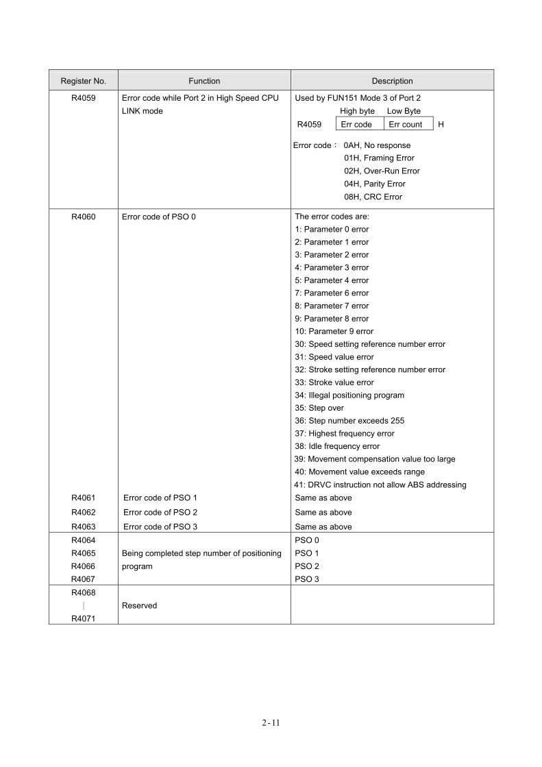
Register No. Function Description
R4059 Error code while Port 2 in High Speed CPU LINK mode
Used by FUN151 Mode 3 of Port 2 High byte Low Byte
R4059 Err code Err count H Error code: 0AH, No response 01H, Framing Error 02H, Over-Run Error 04H, Parity Error 08H, CRC Error
R4060 Error code of PSO 0
The error codes are: 1: Parameter 0 error 2: Parameter 1 error 3: Parameter 2 error 4: Parameter 3 error 5: Parameter 4 error 7: Parameter 6 error 8: Parameter 7 error 9: Parameter 8 error 10: Parameter 9 error 30: Speed setting reference number error 31: Speed value error 32: Stroke setting reference number error 33: Stroke value error 34: Illegal positioning program 35: Step over 36: Step number exceeds 255 37: Highest frequency error 38: Idle frequency error 39: Movement compensation value too large 40: Movement value exceeds range 41: DRVC instruction not allow ABS addressing
R4061 Error code of PSO 1 Same as above
R4062 Error code of PSO 2 Same as above
R4063 Error code of PSO 3 Same as above R4064 PSO 0 R4065
R4066 Being completed step number of positioning program
PSO 1 PSO 2
R4067 PSO 3 R4068
│ R4071
Reserved
2-12
Register No. Function Description
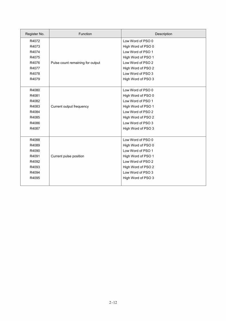
R4072 R4073 R4074 R4075 R4076 R4077 R4078 R4079
Pulse count remaining for output
Low Word of PSO 0 High Word of PSO 0 Low Word of PSO 1 High Word of PSO 1 Low Word of PSO 2 High Word of PSO 2 Low Word of PSO 3 High Word of PSO 3
R4080 Low Word of PSO 0 R4081 High Word of PSO 0 R4082 Low Word of PSO 1 R4083 R4084
Current output frequency High Word of PSO 1 Low Word of PSO 2
R4085 High Word of PSO 2
R4086 R4087
Low Word of PSO 3 High Word of PSO 3
R4088 Low Word of PSO 0 R4089 High Word of PSO 0 R4090 Low Word of PSO 1 R4091 R4092
Current pulse position High Word of PSO 1 Low Word of PSO 2
R4093 R4094
High Word of PSO 2 Low Word of PSO 3
R4095 High Word of PSO 3
2-13
Register No. Function Description
R4096 R4097 R4098 R4099 R4100 R4101 R4102 R4103 R4104 R4105 R4106 R4107 R4108 R4109 R4110 R4111 R4112 R4113 R4114 R4115 R4116 R4117 R4118 R4119 R4120 R4121 R4122 R4123 R4124 R4125 R4126 R4127
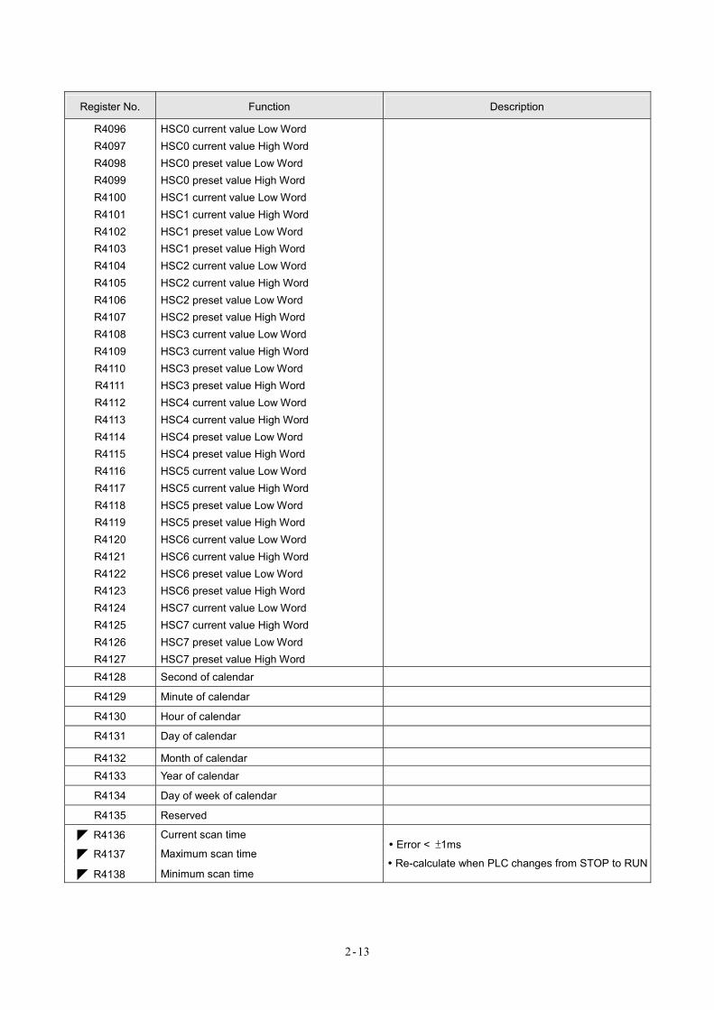
HSC0 current value Low Word HSC0 current value High Word HSC0 preset value Low Word HSC0 preset value High Word HSC1 current value Low Word HSC1 current value High Word HSC1 preset value Low Word HSC1 preset value High Word HSC2 current value Low Word HSC2 current value High Word HSC2 preset value Low Word HSC2 preset value High Word HSC3 current value Low Word HSC3 current value High Word HSC3 preset value Low Word HSC3 preset value High Word HSC4 current value Low Word HSC4 current value High Word HSC4 preset value Low Word HSC4 preset value High Word HSC5 current value Low Word HSC5 current value High Word HSC5 preset value Low Word HSC5 preset value High Word HSC6 current value Low Word HSC6 current value High Word HSC6 preset value Low Word HSC6 preset value High Word HSC7 current value Low Word HSC7 current value High Word HSC7 preset value Low Word HSC7 preset value High Word
R4128 Second of calendar
R4129 Minute of calendar
R4130 Hour of calendar
R4131 Day of calendar
R4132 Month of calendar R4133 Year of calendar
R4134 Day of week of calendar
R4135 Reserved
◤ R4136 Current scan time
◤ R4137 Maximum scan time
◤ R4138 Minimum scan time
Error < ±1ms
Re-calculate when PLC changes from STOP to RUN
2-14
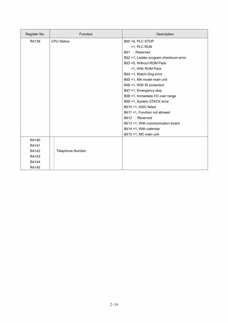
Register No. Function Description
R4139 CPU Status Bit0 =0, PLC STOP =1, PLC RUN Bit1 , Reserved Bit2 =1, Ladder program checksum error Bit3 =0, Without ROM Pack =1, With ROM Pack Bit4 =1, Watch-Dog error Bit5 =1, MA model main unit Bit6 =1, With ID protection Bit7 =1, Emergency stop Bit8 =1, Immediate I/O over range Bit9 =1, System STACK error Bit10 =1, ASIC failed Bit11 =1, Function not allowed Bit12 , Reserved Bit13 =1, With communication board Bit14 =1, With calendar Bit15 =1, MC main unit
R4140 R4141 R4142 R4143 R4144 R4145
Telephone Number
2-15
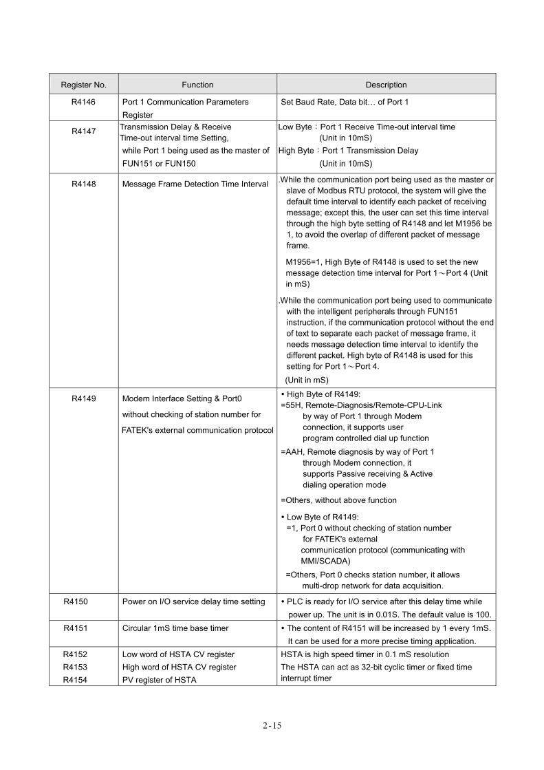
Register No. Function Description
R4146 Port 1 Communication Parameters Register
Set Baud Rate, Data bit… of Port 1
R4147 Transmission Delay & Receive Time-out interval time Setting, while Port 1 being used as the master of FUN151 or FUN150
Low Byte:Port 1 Receive Time-out interval time (Unit in 10mS)
High Byte:Port 1 Transmission Delay (Unit in 10mS)
R4148 Message Frame Detection Time Interval .While the communication port being used as the master or slave of Modbus RTU protocol, the system will give the default time interval to identify each packet of receiving message; except this, the user can set this time interval through the high byte setting of R4148 and let M1956 be 1, to avoid the overlap of different packet of message frame.
M1956=1, High Byte of R4148 is used to set the new message detection time interval for Port 1~Port 4 (Unit in mS)
.While the communication port being used to communicate with the intelligent peripherals through FUN151 instruction, if the communication protocol without the end of text to separate each packet of message frame, it needs message detection time interval to identify the different packet. High byte of R4148 is used for this setting for Port 1~Port 4.
(Unit in mS)
R4149 Modem Interface Setting & Port0
without checking of station number for
FATEK's external communication protocol
High Byte of R4149: =55H, Remote-Diagnosis/Remote-CPU-Link
by way of Port 1 through Modem connection, it supports user program controlled dial up function
=AAH, Remote diagnosis by way of Port 1 through Modem connection, it supports Passive receiving & Active dialing operation mode
=Others, without above function
Low Byte of R4149: =1, Port 0 without checking of station number
for FATEK's external communication protocol (communicating with MMI/SCADA)
=Others, Port 0 checks station number, it allows multi-drop network for data acquisition.
R4150
Power on I/O service delay time setting
PLC is ready for I/O service after this delay time while power up. The unit is in 0.01S. The default value is 100.
R4151
Circular 1mS time base timer
The content of R4151 will be increased by 1 every 1mS. It can be used for a more precise timing application.
R4152 Low word of HSTA CV register HSTA is high speed timer in 0.1 mS resolution R4153 R4154
High word of HSTA CV register PV register of HSTA
The HSTA can act as 32-bit cyclic timer or fixed time interrupt timer
2-16
Register No. Function Description
R4155 Port 1 & Port 2 without station number checking for FATEK's external communication protocol
Low Byte of R4155: =1, Port 1 without station number
checking for FATEK's external communication protocol (communicating with MMI/SCADA)
=Others,Port 1 checks station number, it allows multi-drop network for data acquisition
High Byte of R4155: =1, Port 2 without station number
checking for FATEK's external communication protocol (communicating with MMI/SCADA)
=Others,Port 2 checks station number, it allows multi-drop network for data acquisition
R4156 Port 3 & Port 4 without station number checking for FATEK's external communication protocol
Low Byte of R4156: =1, Port 3 without station number
checking for FATEK's external communication protocol (communicating with MMI/SCADA)
=Others,Port 3 checks station number, it allows multi-drop network for data acquisition
High Byte of R4156: =1, Port 4 without station number
checking for FATEK's external communication protocol (communicating with MMI/SCADA)
=Others,Port 4 checks station number, it allows multi-drop network for data acquisition
R4157 System used
R4158 Port 2 Communication Parameters Register (Not for High Speed CPU Link)
Set Baud Rate, Data bit…of Port 2
R4159 Transmission Delay & Receive Time-out interval time Setting, while Port 2 being used as the master of FUN151 or FUN150
Low Byte:Port 2 Receive Time-out interval time (Unit in 10mS)
High Byte:Port 2 Transmission Delay (Unit in 10mS)
R4160
Port2 RX/TX time out setting for High Speed CPU Link
High Byte of R4160 : =56H, User setting mode if the system default works not
well, Low Byte of R4160 is used for this setting (Not suggest)
=Others, system will give the default value according to the setting of R4161
R4161 Port 2 Communication Parameters Register (For High Speed CPU Link)
Set Baud Rate, Parity…of Port 2 Data bit is fixed to 8-bit Baud Rate≧38400 bps
B7 B6 B5 B4 B3 B2 B1 B0100mS 50mS 10mS 5mS 4mS 3mS 2mS 1mS
R4162
Fixed time interrupt enable/disable control
Bit=0, interrupt enabled Bit=1, interrupt disabled
2-17
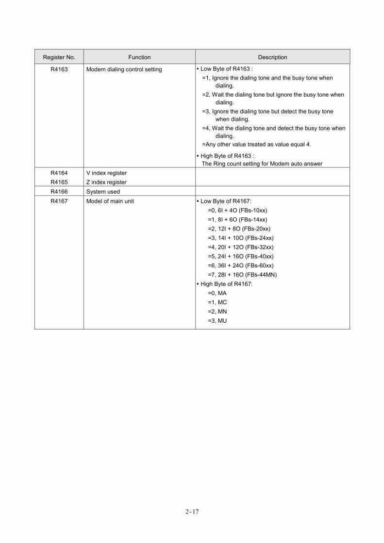
Register No. Function Description
R4163 Modem dialing control setting Low Byte of R4163 : =1, Ignore the dialing tone and the busy tone when
dialing. =2, Wait the dialing tone but ignore the busy tone when
dialing. =3, Ignore the dialing tone but detect the busy tone
when dialing. =4, Wait the dialing tone and detect the busy tone when
dialing. =Any other value treated as value equal 4.
High Byte of R4163 : The Ring count setting for Modem auto answer
R4164 V index register R4165 Z index register R4166 System used R4167 Model of main unit Low Byte of R4167:
=0, 6I + 4O (FBs-10xx) =1, 8I + 6O (FBs-14xx)
=2, 12I + 8O (FBs-20xx) =3, 14I + 10O (FBs-24xx) =4, 20I + 12O (FBs-32xx) =5, 24I + 16O (FBs-40xx) =6, 36I + 24O (FBs-60xx) =7, 28I + 16O (FBs-44MN)
High Byte of R4167: =0, MA
=1, MC =2, MN =3, MU
2-18
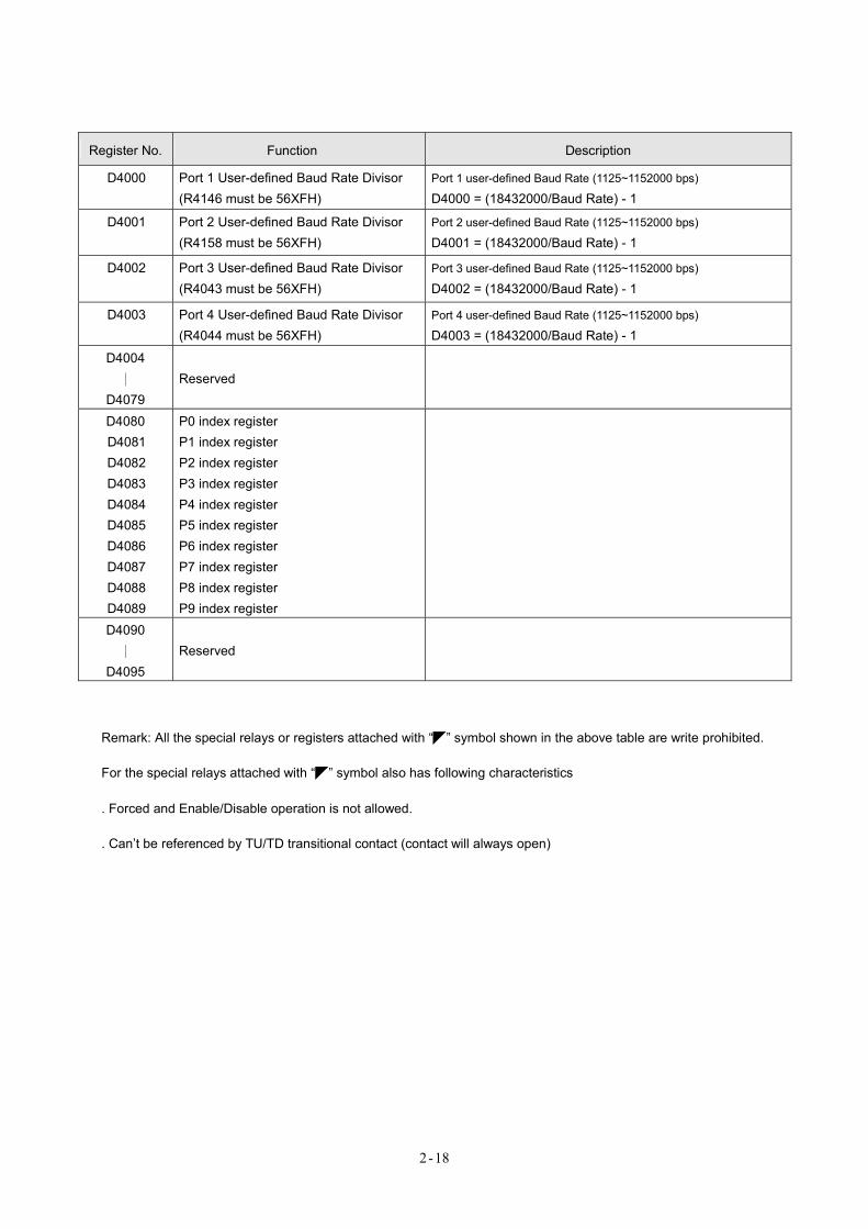
Register No. Function Description
D4000 Port 1 User-defined Baud Rate Divisor (R4146 must be 56XFH)
Port 1 user-defined Baud Rate (1125~1152000 bps)
D4000 = (18432000/Baud Rate) - 1
D4001 Port 2 User-defined Baud Rate Divisor (R4158 must be 56XFH)
Port 2 user-defined Baud Rate (1125~1152000 bps) D4001 = (18432000/Baud Rate) - 1
D4002 Port 3 User-defined Baud Rate Divisor (R4043 must be 56XFH)
Port 3 user-defined Baud Rate (1125~1152000 bps) D4002 = (18432000/Baud Rate) - 1
D4003 Port 4 User-defined Baud Rate Divisor (R4044 must be 56XFH)
Port 4 user-defined Baud Rate (1125~1152000 bps) D4003 = (18432000/Baud Rate) - 1
D4004 │
D4079 Reserved
D4080 D4081 D4082 D4083 D4084 D4085 D4086 D4087 D4088 D4089
P0 index register P1 index register P2 index register P3 index register P4 index register P5 index register P6 index register P7 index register P8 index register P9 index register
D4090 │
D4095 Reserved
Remark: All the special relays or registers attached with “◤” symbol shown in the above table are write prohibited.
For the special relays attached with “◤” symbol also has following characteristics
. Forced and Enable/Disable operation is not allowed.
. Can’t be referenced by TU/TD transitional contact (contact will always open)
3-1
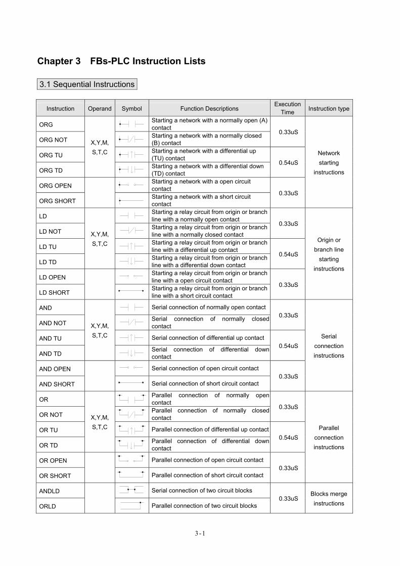
Chapter 3 FBs-PLC Instruction Lists
3.1 Sequential Instructions
Instruction Operand Symbol Function Descriptions Execution
Time Instruction type
ORG Starting a network with a normally open (A) contact
ORG NOT Starting a network with a normally closed (B) contact
0.33uS
ORG TU Starting a network with a differential up (TU) contact
ORG TD
X,Y,M, S,T,C
Starting a network with a differential down (TD) contact
0.54uS
ORG OPEN
Starting a network with a open circuit contact
ORG SHORT
Starting a network with a short circuit contact
0.33uS
Network starting
instructions
LD Starting a relay circuit from origin or branchline with a normally open contact
LD NOT
Starting a relay circuit from origin or branch line with a normally closed contact
0.33uS
LD TU
Starting a relay circuit from origin or branchline with a differential up contact
LD TD
X,Y,M, S,T,C
Starting a relay circuit from origin or branchline with a differential down contact
0.54uS
LD OPEN Starting a relay circuit from origin or branchline with a open circuit contact
LD SHORT
Starting a relay circuit from origin or branchline with a short circuit contact
0.33uS
Origin or branch line
starting instructions
AND Serial connection of normally open contact
AND NOT
Serial connection of normally closed contact
0.33uS
AND TU
Serial connection of differential up contact
AND TD
X,Y,M, S,T,C
Serial connection of differential down contact
0.54uS
AND OPEN Serial connection of open circuit contact
AND SHORT
Serial connection of short circuit contact 0.33uS
Serial connection instructions
OR Parallel connection of normally open contact
OR NOT Parallel connection of normally closed contact
0.33uS
OR TU Parallel connection of differential up contact
OR TD
X,Y,M, S,T,C
Parallel connection of differential down contact
0.54uS
OR OPEN Parallel connection of open circuit contact
OR SHORT
Parallel connection of short circuit contact
0.33uS
Parallel connection instructions
ANDLD
Serial connection of two circuit blocks
ORLD
Parallel connection of two circuit blocks 0.33uS
Blocks merge instructions
3-2
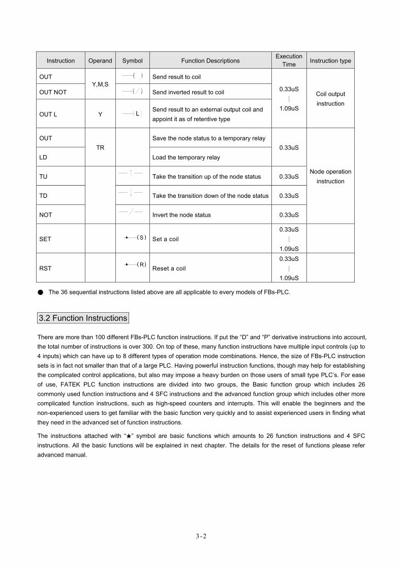
Instruction Operand Symbol Function Descriptions Execution
Time Instruction type
OUT Send result to coil
OUT NOT Y,M,S
Send inverted result to coil
OUT L Y L Send result to an external output coil and appoint it as of retentive type
0.33uS │
1.09uS
Coil output instruction
OUT Save the node status to a temporary relay
LD TR
Load the temporary relay 0.33uS
TU Take the transition up of the node status 0.33uS
TD Take the transition down of the node status 0.33uS
NOT
Invert the node status 0.33uS
Node operation instruction
SET S( )
Set a coil 0.33uS
│ 1.09uS
RST R( )
Reset a coil
0.33uS │
1.09uS
● The 36 sequential instructions listed above are all applicable to every models of FBs-PLC.
3.2 Function Instructions
There are more than 100 different FBs-PLC function instructions. If put the “D” and “P” derivative instructions into account, the total number of instructions is over 300. On top of these, many function instructions have multiple input controls (up to 4 inputs) which can have up to 8 different types of operation mode combinations. Hence, the size of FBs-PLC instruction sets is in fact not smaller than that of a large PLC. Having powerful instruction functions, though may help for establishing the complicated control applications, but also may impose a heavy burden on those users of small type PLC’s. For ease of use, FATEK PLC function instructions are divided into two groups, the Basic function group which includes 26 commonly used function instructions and 4 SFC instructions and the advanced function group which includes other more complicated function instructions, such as high-speed counters and interrupts. This will enable the beginners and the non-experienced users to get familiar with the basic function very quickly and to assist experienced users in finding what they need in the advanced set of function instructions.
The instructions attached with “ ” symbol are basic functions which amounts to 26 function instructions and 4 SFC instructions. All the basic functions will be explained in next chapter. The details for the reset of functions please refer advanced manual.
3-3
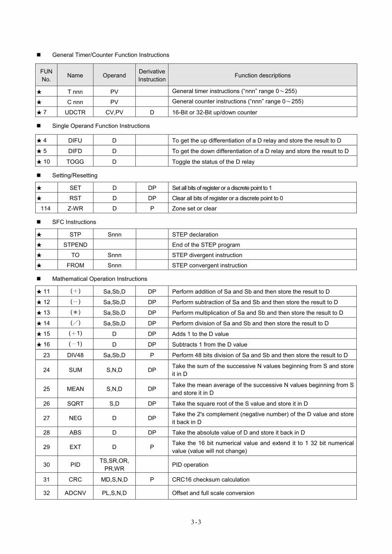
General Timer/Counter Function Instructions
FUN No.
Name Operand Derivative Instruction
Function descriptions
T nnn PV General timer instructions (“nnn” range 0~255)
C nnn PV General counter instructions (“nnn” range 0~255)
7 UDCTR CV,PV D 16-Bit or 32-Bit up/down counter
Single Operand Function Instructions
4 DIFU D To get the up differentiation of a D relay and store the result to D
5 DIFD D To get the down differentiation of a D relay and store the result to D
10 TOGG D Toggle the status of the D relay
Setting/Resetting
SET D DP Set all bits of register or a discrete point to 1
RST D DP Clear all bits of register or a discrete point to 0
114 Z-WR D P Zone set or clear
SFC Instructions
STP Snnn STEP declaration
STPEND End of the STEP program
TO Snnn STEP divergent instruction
FROM Snnn STEP convergent instruction
Mathematical Operation Instructions
11 (+) Sa,Sb,D DP Perform addition of Sa and Sb and then store the result to D
12 (-) Sa,Sb,D DP Perform subtraction of Sa and Sb and then store the result to D
13 (*) Sa,Sb,D DP Perform multiplication of Sa and Sb and then store the result to D
14 (/) Sa,Sb,D DP Perform division of Sa and Sb and then store the result to D
15 (+1) D DP Adds 1 to the D value
16 (-1) D DP Subtracts 1 from the D value
23 DIV48 Sa,Sb,D P Perform 48 bits division of Sa and Sb and then store the result to D
24 SUM S,N,D DP Take the sum of the successive N values beginning from S and store it in D
25 MEAN S,N,D DP Take the mean average of the successive N values beginning from S and store it in D
26 SQRT S,D DP Take the square root of the S value and store it in D
27 NEG D DP Take the 2's complement (negative number) of the D value and store it back in D
28 ABS D DP Take the absolute value of D and store it back in D
29 EXT D P Take the 16 bit numerical value and extend it to 1 32 bit numerical value (value will not change)
30 PID TS,SR,OR,
PR,WR PID operation
31 CRC MD,S,N,D P CRC16 checksum calculation
32 ADCNV PL,S,N,D Offset and full scale conversion
3-4
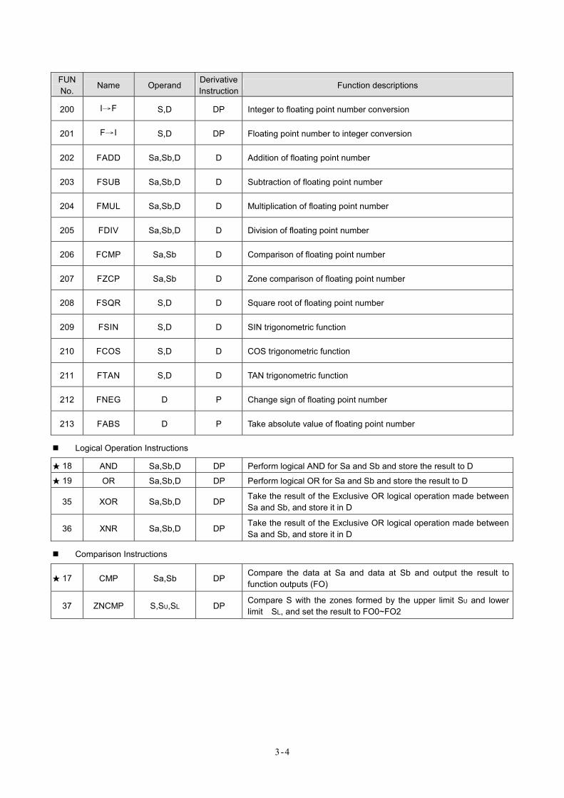
FUN No.
Name Operand Derivative Instruction
Function descriptions
200 I→F S,D DP Integer to floating point number conversion
201 F→I S,D DP Floating point number to integer conversion
202 FADD Sa,Sb,D D Addition of floating point number
203 FSUB Sa,Sb,D D Subtraction of floating point number
204 FMUL Sa,Sb,D D Multiplication of floating point number
205 FDIV Sa,Sb,D D Division of floating point number
206 FCMP Sa,Sb D Comparison of floating point number
207 FZCP Sa,Sb D Zone comparison of floating point number
208 FSQR S,D D Square root of floating point number
209 FSIN S,D D SIN trigonometric function
210 FCOS S,D D COS trigonometric function
211 FTAN S,D D TAN trigonometric function
212 FNEG D P Change sign of floating point number
213 FABS D P Take absolute value of floating point number
Logical Operation Instructions
18 AND Sa,Sb,D DP Perform logical AND for Sa and Sb and store the result to D
19 OR Sa,Sb,D DP Perform logical OR for Sa and Sb and store the result to D
35 XOR Sa,Sb,D DP Take the result of the Exclusive OR logical operation made between Sa and Sb, and store it in D
36 XNR Sa,Sb,D DP Take the result of the Exclusive OR logical operation made between Sa and Sb, and store it in D
Comparison Instructions
17 CMP Sa,Sb DP Compare the data at Sa and data at Sb and output the result to function outputs (FO)
37 ZNCMP S,SU,SL DP Compare S with the zones formed by the upper limit SU and lower limit SL, and set the result to FO0~FO2
3-5
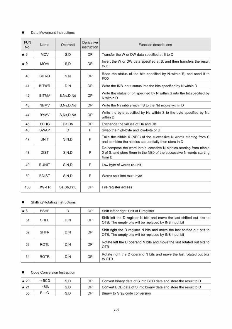
Data Movement Instructions
FUN No.
Name Operand Derivativeinstruction
Function descriptions
8 MOV S,D DP Transfer the W or DW data specified at S to D
9 MOV/ S,D DP Invert the W or DW data specified at S, and then transfers the result to D
40 BITRD S,N DP Read the status of the bits specified by N within S, and send it to FO0
41 BITWR D,N DP Write the INB input status into the bits specified by N within D
42 BITMV S,Ns,D,Nd DP Write the status of bit specified by N within S into the bit specified by N within D
43 NBMV S,Ns,D,Nd DP Write the Ns nibble within S to the Nd nibble within D
44 BYMV S,Ns,D,Nd DP Write the byte specified by Ns within S to the byte specified by Nd within D
45 XCHG Da,Db DP Exchange the values of Da and Db
46 SWAP D P Swap the high-byte and low-byte of D
47 UNIT S,N,D P Take the nibble 0 (NB0) of the successive N words starting from S and combine the nibbles sequentially then store in D
48 DIST S,N,D P De-compose the word into successive N nibbles starting from nibble 0 of S, and store them in the NB0 of the successive N words starting from D
49 BUNIT S,N,D P Low byte of words re-unit
50 BDIST S,N,D P Words split into multi-byte
160 RW-FR Sa,Sb,Pr,L DP File register access
Shifting/Rotating Instructions
6 BSHF D DP Shift left or right 1 bit of D register
51 SHFL D,N DP Shift left the D register N bits and move the last shifted out bits to OTB. The empty bits will be replaced by INB input bit
52 SHFR D,N DP Shift right the D register N bits and move the last shifted out bits to OTB, The empty bits will be replaced by INB input bit
53 ROTL D,N DP Rotate left the D operand N bits and move the last rotated out bits to OTB
54 ROTR D,N DP Rotate right the D operand N bits and move the last rotated out bits to OTB
Code Conversion Instruction
20 →BCD S,D DP Convert binary data of S into BCD data and store the result to D
21 →BIN S,D DP Convert BCD data of S into binary data and store the result to D
55 B→G S,D DP Binary to Gray code conversion
3-6
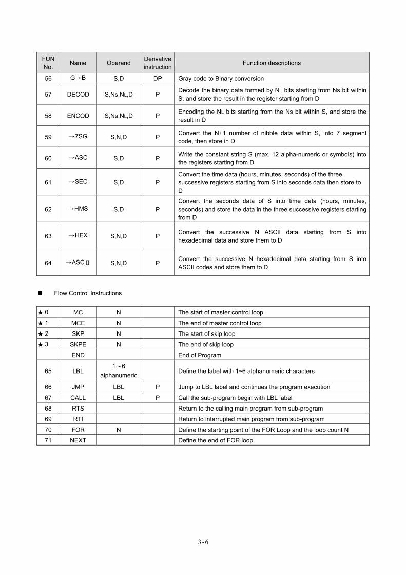
FUN No.
Name Operand Derivativeinstruction
Function descriptions
56 G→B S,D DP Gray code to Binary conversion
57 DECOD S,Ns,NL,D P Decode the binary data formed by NL bits starting from Ns bit within S, and store the result in the register starting from D
58 ENCOD S,Ns,NL,D P Encoding the NL bits starting from the Ns bit within S, and store the result in D
59 →7SG S,N,D P Convert the N+1 number of nibble data within S, into 7 segment code, then store in D
60 →ASC S,D P Write the constant string S (max. 12 alpha-numeric or symbols) into the registers starting from D
61 →SEC S,D P Convert the time data (hours, minutes, seconds) of the three successive registers starting from S into seconds data then store to D
62 →HMS S,D P Convert the seconds data of S into time data (hours, minutes, seconds) and store the data in the three successive registers starting from D
63 →HEX S,N,D P Convert the successive N ASCII data starting from S into hexadecimal data and store them to D
64 →ASCⅡ S,N,D P Convert the successive N hexadecimal data starting from S into ASCII codes and store them to D
Flow Control Instructions
0 MC N The start of master control loop
1 MCE N The end of master control loop
2 SKP N The start of skip loop
3 SKPE N The end of skip loop
END End of Program
65 LBL 1~6
alphanumeric Define the label with 1~6 alphanumeric characters
66 JMP LBL P Jump to LBL label and continues the program execution
67 CALL LBL P Call the sub-program begin with LBL label
68 RTS Return to the calling main program from sub-program
69 RTI Return to interrupted main program from sub-program
70 FOR N Define the starting point of the FOR Loop and the loop count N
71 NEXT Define the end of FOR loop
3-7
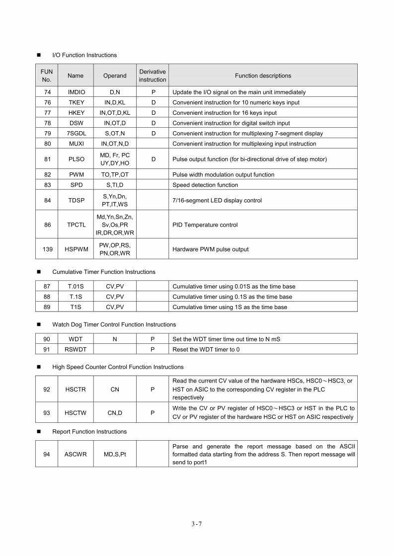
I/O Function Instructions
FUN No.
Name Operand Derivativeinstruction
Function descriptions
74 IMDIO D,N P Update the I/O signal on the main unit immediately
76 TKEY IN,D,KL D Convenient instruction for 10 numeric keys input
77 HKEY IN,OT,D,KL D Convenient instruction for 16 keys input
78 DSW IN,OT,D D Convenient instruction for digital switch input
79 7SGDL S,OT,N D Convenient instruction for multiplexing 7-segment display
80 MUXI IN,OT,N,D Convenient instruction for multiplexing input instruction
81 PLSO MD, Fr, PC UY,DY,HO
D Pulse output function (for bi-directional drive of step motor)
82 PWM TO,TP,OT Pulse width modulation output function
83 SPD S,TI,D Speed detection function
84 TDSP S,Yn,Dn, PT,IT,WS
7/16-segment LED display control
86 TPCTL Md,Yn,Sn,Zn,
Sv,Os,PR IR,DR,OR,WR
PID Temperature control
139 HSPWM PW,OP,RS, PN,OR,WR
Hardware PWM pulse output
Cumulative Timer Function Instructions
87 T.01S CV,PV Cumulative timer using 0.01S as the time base
88 T.1S CV,PV Cumulative timer using 0.1S as the time base
89 T1S CV,PV Cumulative timer using 1S as the time base
Watch Dog Timer Control Function Instructions
90 WDT N P Set the WDT timer time out time to N mS
91 RSWDT P Reset the WDT timer to 0
High Speed Counter Control Function Instructions
92 HSCTR CN P Read the current CV value of the hardware HSCs, HSC0~HSC3, or HST on ASIC to the corresponding CV register in the PLC respectively
93 HSCTW CN,D P Write the CV or PV register of HSC0~HSC3 or HST in the PLC to CV or PV register of the hardware HSC or HST on ASIC respectively
Report Function Instructions
94 ASCWR MD,S,Pt Parse and generate the report message based on the ASCII formatted data starting from the address S. Then report message will send to port1
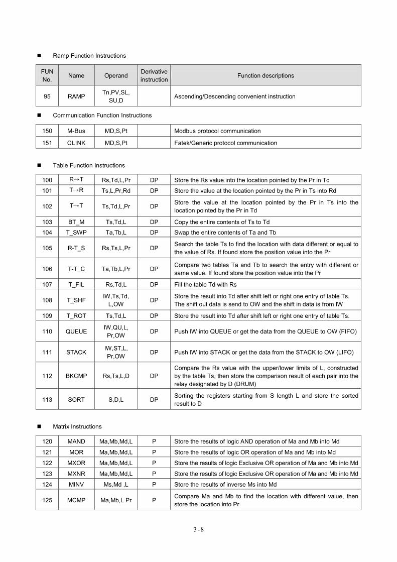
3-8
Ramp Function Instructions
FUN No.
Name Operand Derivativeinstruction
Function descriptions
95 RAMP Tn,PV,SL,
SU,D Ascending/Descending convenient instruction
Communication Function Instructions
150 M-Bus MD,S,Pt Modbus protocol communication
151 CLINK MD,S,Pt Fatek/Generic protocol communication
Table Function Instructions
100 R→T Rs,Td,L,Pr DP Store the Rs value into the location pointed by the Pr in Td
101 T→R Ts,L,Pr,Rd DP Store the value at the location pointed by the Pr in Ts into Rd
102 T→T Ts,Td,L,Pr DP Store the value at the location pointed by the Pr in Ts into the location pointed by the Pr in Td
103 BT_M Ts,Td,L DP Copy the entire contents of Ts to Td
104 T_SWP Ta,Tb,L DP Swap the entire contents of Ta and Tb
105 R-T_S Rs,Ts,L,Pr DP Search the table Ts to find the location with data different or equal to the value of Rs. If found store the position value into the Pr
106 T-T_C Ta,Tb,L,Pr DP Compare two tables Ta and Tb to search the entry with different or same value. If found store the position value into the Pr
107 T_FIL Rs,Td,L DP Fill the table Td with Rs
108 T_SHF IW,Ts,Td,
L,OW DP
Store the result into Td after shift left or right one entry of table Ts. The shift out data is send to OW and the shift in data is from IW
109 T_ROT Ts,Td,L DP Store the result into Td after shift left or right one entry of table Ts.
110 QUEUE IW,QU,L, Pr,OW
DP Push IW into QUEUE or get the data from the QUEUE to OW (FIFO)
111 STACK IW,ST,L, Pr,OW
DP Push IW into STACK or get the data from the STACK to OW (LIFO)
112 BKCMP Rs,Ts,L,D DP Compare the Rs value with the upper/lower limits of L, constructed by the table Ts, then store the comparison result of each pair into the relay designated by D (DRUM)
113 SORT S,D,L DP Sorting the registers starting from S length L and store the sorted result to D
Matrix Instructions
120 MAND Ma,Mb,Md,L P Store the results of logic AND operation of Ma and Mb into Md
121 MOR Ma,Mb,Md,L P Store the results of logic OR operation of Ma and Mb into Md
122 MXOR Ma,Mb,Md,L P Store the results of logic Exclusive OR operation of Ma and Mb into Md
123 MXNR Ma,Mb,Md,L P Store the results of logic Exclusive OR operation of Ma and Mb into Md
124 MINV Ms,Md ,L P Store the results of inverse Ms into Md
125 MCMP Ma,Mb,L Pr P Compare Ma and Mb to find the location with different value, then store the location into Pr
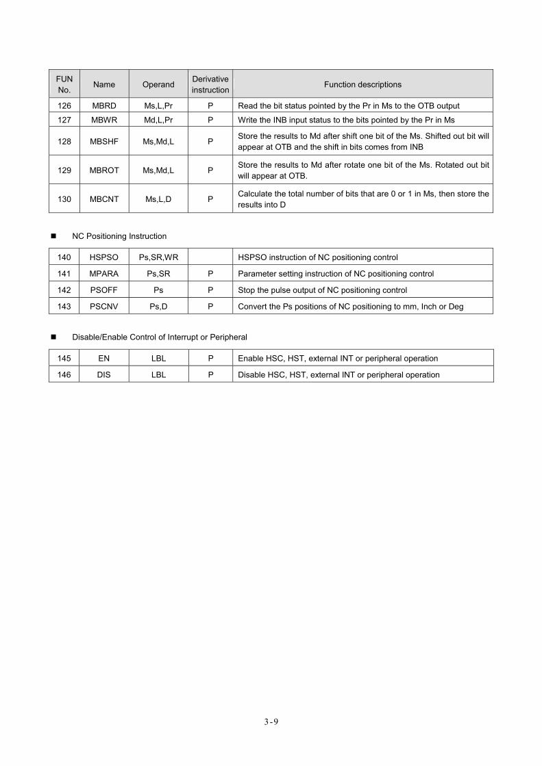
3-9
FUN No.
Name Operand Derivativeinstruction
Function descriptions
126 MBRD Ms,L,Pr P Read the bit status pointed by the Pr in Ms to the OTB output
127 MBWR Md,L,Pr P Write the INB input status to the bits pointed by the Pr in Ms
128 MBSHF Ms,Md,L P Store the results to Md after shift one bit of the Ms. Shifted out bit will appear at OTB and the shift in bits comes from INB
129 MBROT Ms,Md,L P Store the results to Md after rotate one bit of the Ms. Rotated out bit will appear at OTB.
130 MBCNT Ms,L,D P Calculate the total number of bits that are 0 or 1 in Ms, then store the results into D
NC Positioning Instruction
140 HSPSO Ps,SR,WR HSPSO instruction of NC positioning control
141 MPARA Ps,SR P Parameter setting instruction of NC positioning control
142 PSOFF Ps P Stop the pulse output of NC positioning control
143 PSCNV Ps,D P Convert the Ps positions of NC positioning to mm, Inch or Deg
Disable/Enable Control of Interrupt or Peripheral
145 EN LBL P Enable HSC, HST, external INT or peripheral operation
146 DIS LBL P Disable HSC, HST, external INT or peripheral operation

MEMO
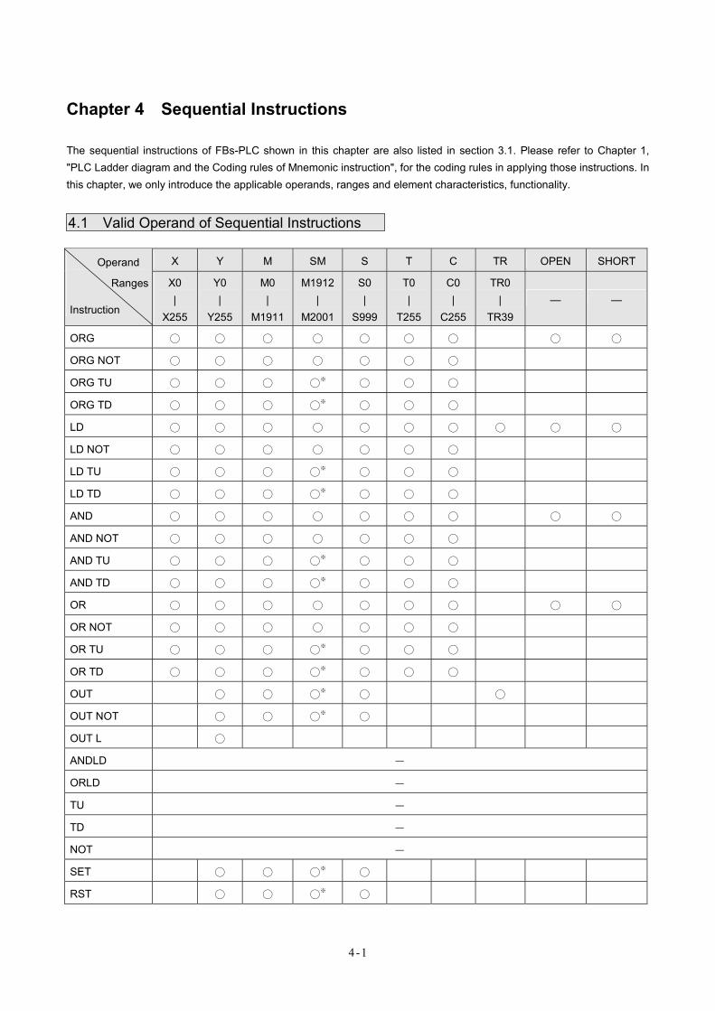
4-1
Chapter 4 Sequential Instructions
The sequential instructions of FBs-PLC shown in this chapter are also listed in section 3.1. Please refer to Chapter 1, "PLC Ladder diagram and the Coding rules of Mnemonic instruction", for the coding rules in applying those instructions. In this chapter, we only introduce the applicable operands, ranges and element characteristics, functionality.
4.1 Valid Operand of Sequential Instructions
X Y M SM S T C TR OPEN SHORT Operand
Ranges
Instruction
X0 |
X255
Y0 |
Y255
M0 |
M1911
M1912|
M2001
S0 |
S999
T0 |
T255
C0 |
C255
TR0 |
TR39 — —
ORG ○ ○ ○ ○ ○ ○ ○ ○ ○
ORG NOT ○ ○ ○ ○ ○ ○ ○
ORG TU ○ ○ ○ ○※ ○ ○ ○
ORG TD ○ ○ ○ ○※ ○ ○ ○
LD ○ ○ ○ ○ ○ ○ ○ ○ ○ ○
LD NOT ○ ○ ○ ○ ○ ○ ○
LD TU ○ ○ ○ ○※ ○ ○ ○
LD TD ○ ○ ○ ○※ ○ ○ ○
AND ○ ○ ○ ○ ○ ○ ○ ○ ○
AND NOT ○ ○ ○ ○ ○ ○ ○
AND TU ○ ○ ○ ○※ ○ ○ ○
AND TD ○ ○ ○ ○※ ○ ○ ○
OR ○ ○ ○ ○ ○ ○ ○ ○ ○
OR NOT ○ ○ ○ ○ ○ ○ ○
OR TU ○ ○ ○ ○※ ○ ○ ○
OR TD ○ ○ ○ ○※ ○ ○ ○
OUT ○ ○ ○※ ○ ○
OUT NOT ○ ○ ○※ ○
OUT L ○
ANDLD −
ORLD −
TU −
TD −
NOT −
SET ○ ○ ○※ ○
RST ○ ○ ○※ ○
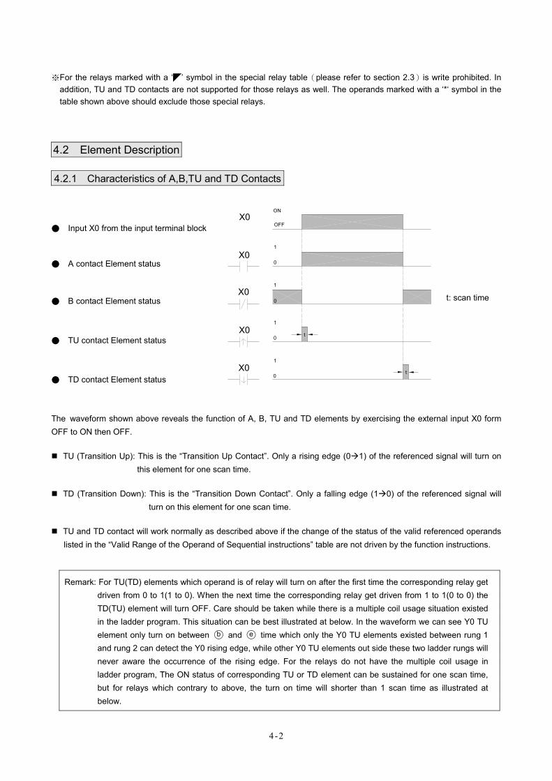
4-2
※For the relays marked with a ‘◤’ symbol in the special relay table(please refer to section 2.3)is write prohibited. In addition, TU and TD contacts are not supported for those relays as well. The operands marked with a ‘*‘ symbol in the table shown above should exclude those special relays.
4.2 Element Description
4.2.1 Characteristics of A,B,TU and TD Contacts
● Input X0 from the input terminal block
● A contact Element status
● B contact Element status
● TU contact Element status
● TD contact Element status
X0
X0
X0
X0
X0
ON
OFF
1
0
1
0
1
0
1
0
t
t
t: scan time
The waveform shown above reveals the function of A, B, TU and TD elements by exercising the external input X0 form OFF to ON then OFF.
TU (Transition Up): This is the “Transition Up Contact”. Only a rising edge (0 1) of the referenced signal will turn on this element for one scan time.
TD (Transition Down): This is the “Transition Down Contact”. Only a falling edge (1 0) of the referenced signal will turn on this element for one scan time.
TU and TD contact will work normally as described above if the change of the status of the valid referenced operands listed in the “Valid Range of the Operand of Sequential instructions” table are not driven by the function instructions.
Remark: For TU(TD) elements which operand is of relay will turn on after the first time the corresponding relay get driven from 0 to 1(1 to 0). When the next time the corresponding relay get driven from 1 to 1(0 to 0) the TD(TU) element will turn OFF. Care should be taken while there is a multiple coil usage situation existed in the ladder program. This situation can be best illustrated at below. In the waveform we can see Y0 TU element only turn on between ○b and ○e time which only the Y0 TU elements existed between rung 1 and rung 2 can detect the Y0 rising edge, while other Y0 TU elements out side these two ladder rungs will never aware the occurrence of the rising edge. For the relays do not have the multiple coil usage in ladder program, The ON status of corresponding TU or TD element can be sustained for one scan time, but for relays which contrary to above, the turn on time will shorter than 1 scan time as illustrated at below.
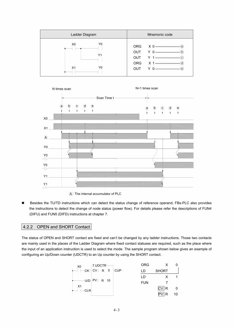
4-3
Ladder Diagram Mnemonic code
X0 Y0
Y1
Y0X1
ORG X 0 ---------------------○a OUT Y 0 ---------------------○b OUT Y 1 ---------------------○c ORG X 1 ---------------------○d OUT Y 0 ---------------------○e
N times scan
Scan Time t
N+1 times scan
a b c d e
X0
X1
Y0
A
Y0
Y0
Y1
Y1
A : The internal accumulator of PLC
a b c d e
Besides the TU/TD instructions which can detect the status change of reference operand, FBs-PLC also provides the instructions to detect the change of node status (power flow). For details please refer the descriptions of FUN4 (DIFU) and FUN5 (DIFD) instructions at chapter 7.
4.2.2 OPEN and SHORT Contact
The status of OPEN and SHORT contact are fixed and can’t be changed by any ladder instructions. Those two contacts are mainly used in the places of the Ladder Diagram where fixed contact statuses are required, such as the place where the input of an application instruction is used to select the mode. The sample program shown below gives an example of configuring an Up/Down counter (UDCTR) to an Up counter by using the SHORT contact.
ORG X 0
LD SHORT
LD X 1 FUN 7 CV: R 0
X0
X1
7.UDCTRCV :
PV :U/D
R 0
10R
CUPCK
CLR
PV: R 10
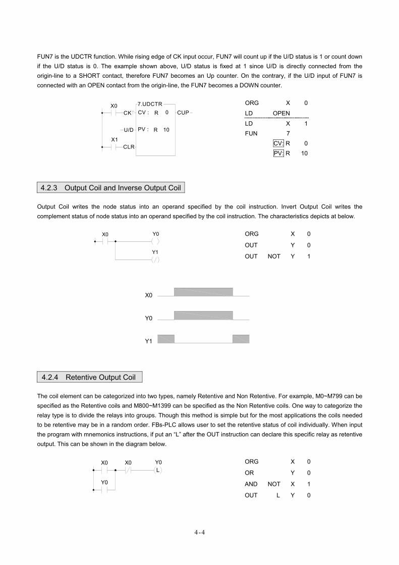
4-4
FUN7 is the UDCTR function. While rising edge of CK input occur, FUN7 will count up if the U/D status is 1 or count down if the U/D status is 0. The example shown above, U/D status is fixed at 1 since U/D is directly connected from the origin-line to a SHORT contact, therefore FUN7 becomes an Up counter. On the contrary, if the U/D input of FUN7 is connected with an OPEN contact from the origin-line, the FUN7 becomes a DOWN counter.
ORG X 0
LD OPEN
LD X 1 FUN 7 CV: R 0
X0
X1
7.UDCTRCV :
PV :
CK
U/D
CLR
R 0
10R
CUP
PV: R 10
4.2.3 Output Coil and Inverse Output Coil
Output Coil writes the node status into an operand specified by the coil instruction. Invert Output Coil writes the complement status of node status into an operand specified by the coil instruction. The characteristics depicts at below.
ORG X 0
OUT Y 0
Y0
Y1
X0
OUT NOT Y 1
X0
Y0
Y1
4.2.4 Retentive Output Coil
The coil element can be categorized into two types, namely Retentive and Non Retentive. For example, M0~M799 can be specified as the Retentive coils and M800~M1399 can be specified as the Non Retentive coils. One way to categorize the relay type is to divide the relays into groups. Though this method is simple but for the most applications the coils needed to be retentive may be in a random order. FBs-PLC allows user to set the retentive status of coil individually. When input the program with mnemonics instructions, if put an “L” after the OUT instruction can declare this specific relay as retentive output. This can be shown in the diagram below.
ORG X 0
OR Y 0
AND NOT X 1
X0 Y0
Y0
X0L
OUT L Y 0
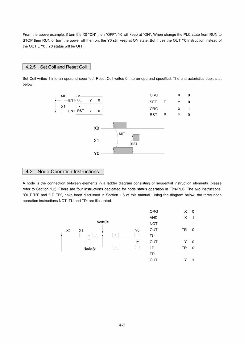
4-5
From the above example, if turn the X0 "ON" then "OFF", Y0 will keep at "ON". When change the PLC state from RUN to STOP then RUN or turn the power off then on, the Y0 still keep at ON state. But if use the OUT Y0 instruction instead of the OUT L Y0 , Y0 status will be OFF.
4.2.5 Set Coil and Reset Coil
Set Coil writes 1 into an operand specified. Reset Coil writes 0 into an operand specified. The characteristics depicts at below.
ORG X 0
SET P Y 0 PSET Y 0
X0
X1
EN
PRST Y 0EN
ORG RST
P
X Y
1 0
X0
X1
Y0
SET
RST
4.3 Node Operation Instructions
A node is the connection between elements in a ladder diagram consisting of sequential instruction elements (please refer to Section 1.2). There are four instructions dedicated for node status operation in FBs-PLC. The two instructions, “OUT TR” and “LD TR”, have been discussed in Section 1.6 of this manual. Using the diagram below, the three node operation instructions NOT, TU and TD, are illustrated.
ORG X 0
AND X 1 NOT OUT TR 0 TU OUT Y 0 LD TR 0 TD
X0 Y0
Y1
Node A
Node B
X1
OUT Y 1
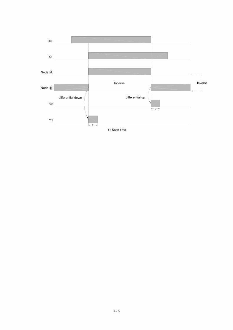
4-6
X0
X1
Node A
Y0
Y1
Node B
differential down
Incerse
differential up
t : Scan time
Inverse
t
t
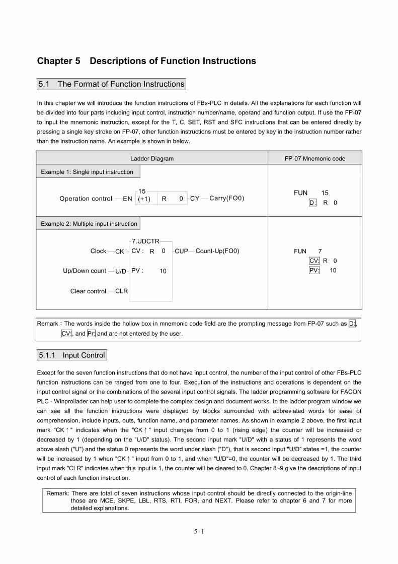
5-1
Chapter 5 Descriptions of Function Instructions
5.1 The Format of Function Instructions
In this chapter we will introduce the function instructions of FBs-PLC in details. All the explanations for each function will be divided into four parts including input control, instruction number/name, operand and function output. If use the FP-07 to input the mnemonic instruction, except for the T, C, SET, RST and SFC instructions that can be entered directly by pressing a single key stroke on FP-07, other function instructions must be entered by key in the instruction number rather than the instruction name. An example is shown in below.
Ladder Diagram FP-07 Mnemonic code
Example 1: Single input instruction
0EN15
Operation control (+1) R CY Carry(FO0)
FUN 15 D : R 0
Example 2: Multiple input instruction
7.UDCTRCV :
PV :
CK
U/D
CLR
R 0
10
CUPClock
Up/Down count
Clear control
Count-Up(FO0)
FUN 7 CV: R 0 PV: 10
Remark:The words inside the hollow box in mnemonic code field are the prompting message from FP-07 such as D:, CV:, and Pr: and are not entered by the user.
5.1.1 Input Control
Except for the seven function instructions that do not have input control, the number of the input control of other FBs-PLC function instructions can be ranged from one to four. Execution of the instructions and operations is dependent on the input control signal or the combinations of the several input control signals. The ladder programming software for FACON PLC - Winprollader can help user to complete the complex design and document works. In the ladder program window we can see all the function instructions were displayed by blocks surrounded with abbreviated words for ease of comprehension, include inputs, outs, function name, and parameter names. As shown in example 2 above, the first input mark "CK↑" indicates when the "CK↑" input changes from 0 to 1 (rising edge) the counter will be increased or decreased by 1 (depending on the "U/D" status). The second input mark "U/D" with a status of 1 represents the word above slash ("U") and the status 0 represents the word under slash ("D"), that is second input "U/D" states =1, the counter will be increased by 1 when "CK↑" input from 0 to 1, and when "U/D"=0, the counter will be decreased by 1. The third input mark "CLR" indicates when this input is 1, the counter will be cleared to 0. Chapter 8~9 give the descriptions of input control of each function instruction.
Remark: There are total of seven instructions whose input control should be directly connected to the origin-line those are MCE, SKPE, LBL, RTS, RTI, FOR, and NEXT. Please refer to chapter 6 and 7 for more detailed explanations.
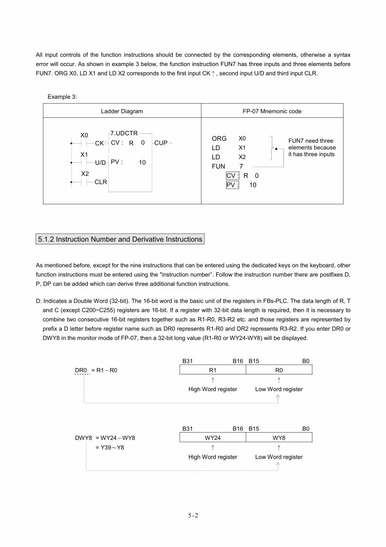
5-2
All input controls of the function instructions should be connected by the corresponding elements, otherwise a syntax error will occur. As shown in example 3 below, the function instruction FUN7 has three inputs and three elements before FUN7. ORG X0, LD X1 and LD X2 corresponds to the first input CK↑, second input U/D and third input CLR.
Example 3:
Ladder Diagram FP-07 Mnemonic code
X0
X2
7.UDCTRCV :
PV :
CLR
R 0
10
CUP
X1U/D
CK
ORG LD LD FUN 7
CV : R 0 PV : 10
FUN7 need three elements because it has three inputs
5.1.2 Instruction Number and Derivative Instructions
As mentioned before, except for the nine instructions that can be entered using the dedicated keys on the keyboard, other function instructions must be entered using the "instruction number”. Follow the instruction number there are postfixes D, P, DP can be added which can derive three additional function instructions.
D: Indicates a Double Word (32-bit). The 16-bit word is the basic unit of the registers in FBs-PLC. The data length of R, T and C (except C200~C255) registers are 16-bit. If a register with 32-bit data length is required, then it is necessary to combine two consecutive 16-bit registers together such as R1-R0, R3-R2 etc. and those registers are represented by prefix a D letter before register name such as DR0 represents R1-R0 and DR2 represents R3-R2. If you enter DR0 or DWY8 in the monitor mode of FP-07, then a 32-bit long value (R1-R0 or WY24-WY8) will be displayed.
B31 B16 B15 B0 DR0 = R1−R0 R1 R0 ↑ ↑ High Word register Low Word register
B31 B16 B15 B0 DWY8 = WY24−WY8 WY24 WY8 = Y39~Y8 ↑ ↑ High Word register Low Word register
X0 X1 X2
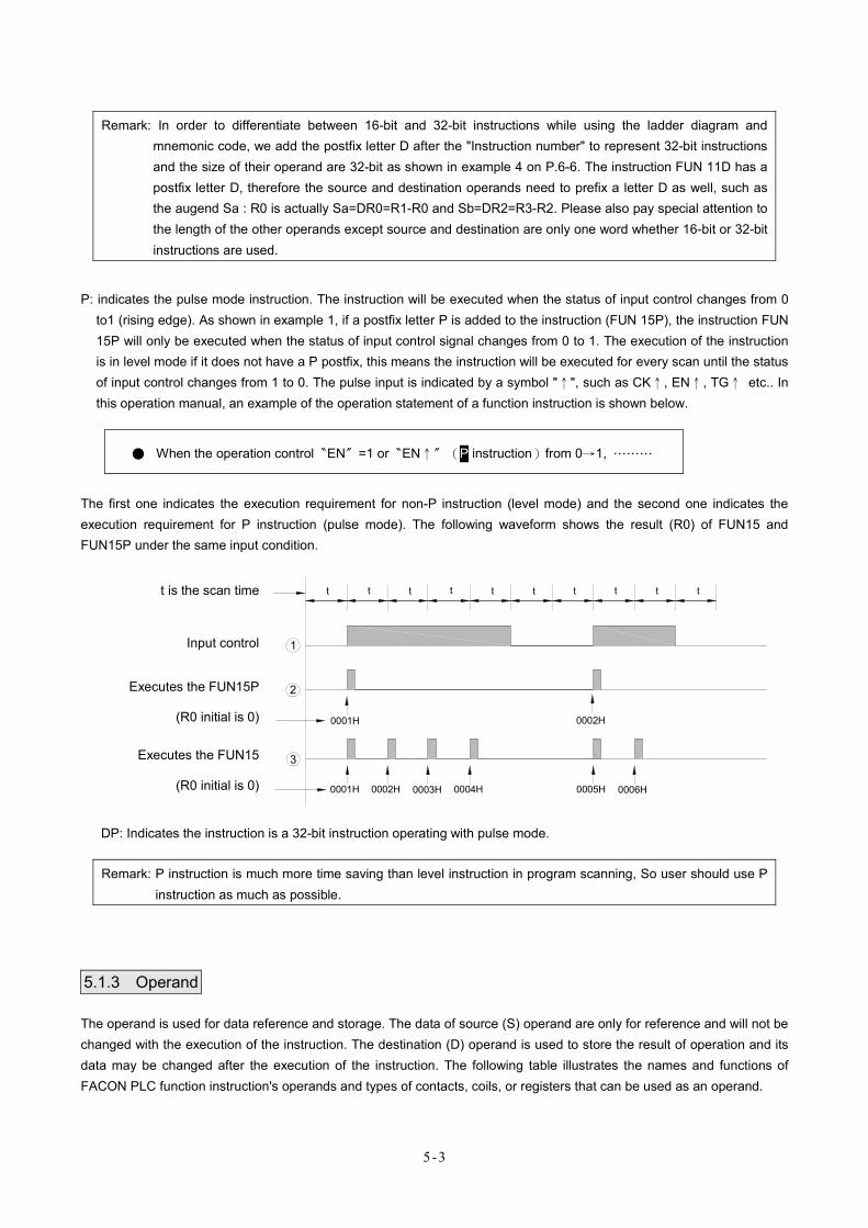
5-3
Remark: In order to differentiate between 16-bit and 32-bit instructions while using the ladder diagram and mnemonic code, we add the postfix letter D after the "Instruction number" to represent 32-bit instructions and the size of their operand are 32-bit as shown in example 4 on P.6-6. The instruction FUN 11D has a postfix letter D, therefore the source and destination operands need to prefix a letter D as well, such as the augend Sa : R0 is actually Sa=DR0=R1-R0 and Sb=DR2=R3-R2. Please also pay special attention to the length of the other operands except source and destination are only one word whether 16-bit or 32-bit instructions are used.
P: indicates the pulse mode instruction. The instruction will be executed when the status of input control changes from 0 to1 (rising edge). As shown in example 1, if a postfix letter P is added to the instruction (FUN 15P), the instruction FUN 15P will only be executed when the status of input control signal changes from 0 to 1. The execution of the instruction is in level mode if it does not have a P postfix, this means the instruction will be executed for every scan until the status of input control changes from 1 to 0. The pulse input is indicated by a symbol "↑", such as CK↑, EN↑, TG↑ etc.. In this operation manual, an example of the operation statement of a function instruction is shown below.
● When the operation control〝EN〞=1 or〝EN↑〞(P instruction)from 0→1, ………
The first one indicates the execution requirement for non-P instruction (level mode) and the second one indicates the execution requirement for P instruction (pulse mode). The following waveform shows the result (R0) of FUN15 and FUN15P under the same input condition.
t is the scan time
Input control
Executes the FUN15P
(R0 initial is 0)
Executes the FUN15
(R0 initial is 0)
1
2
3
0001H
0001H 0002H 0003H 0004H
0002H
0005H 0006H
t t t t t t t t t t
DP: Indicates the instruction is a 32-bit instruction operating with pulse mode.
Remark: P instruction is much more time saving than level instruction in program scanning, So user should use P instruction as much as possible.
5.1.3 Operand
The operand is used for data reference and storage. The data of source (S) operand are only for reference and will not be changed with the execution of the instruction. The destination (D) operand is used to store the result of operation and its data may be changed after the execution of the instruction. The following table illustrates the names and functions of FACON PLC function instruction's operands and types of contacts, coils, or registers that can be used as an operand.
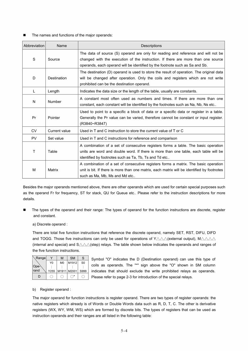
5-4
The names and functions of the major operands:
Abbreviation Name Descriptions
S Source The data of source (S) operand are only for reading and reference and will not be changed with the execution of the instruction. If there are more than one source operands, each operand will be identified by the footnote such as Sa and Sb.
D Destination The destination (D) operand is used to store the result of operation. The original data will be changed after operation. Only the coils and registers which are not write prohibited can be the destination operand.
L Length Indicates the data size or the length of the table, usually are constants.
N Number A constant most often used as numbers and times. If there are more than one constant, each constant will be identified by the footnotes such as Na, Nb, Ns etc..
Pr Pointer Used to point to a specific a block of data or a specific data or register in a table. Generally the Pr value can be varied, therefore cannot be constant or input register. (R3840~R3847)
CV Current value Used in T and C instruction to store the current value of T or C
PV Set value Used in T and C instructions for reference and comparison
T Table A combination of a set of consecutive registers forms a table. The basic operation units are word and double word. If there is more than one table, each table will be identified by footnotes such as Ta, Tb, Ts and Td etc..
M Matrix A combination of a set of consecutive registers forms a matrix. The basic operation unit is bit. If there is more than one matrix, each matrix will be identified by footnotes such as Ma, Mb, Ms and Md etc..
Besides the major operands mentioned above, there are other operands which are used for certain special purposes such as the operand Fr for frequency, ST for stack, QU for Queue etc.. Please refer to the instruction descriptions for more details.
The types of the operand and their range: The types of operand for the function instructions are discrete, register and constant.
a) Discrete operand :
There are total five function instructions that reference the discrete operand, namely SET, RST, DIFU, DIFD and TOGG. Those five instructions can only be used for operations of Y△△△(external output), M△△△△
(internal and special) and S△△△(step) relays. The table shown below indicates the operands and ranges of the five function instructions.
Y M SM S Range
Ope- rand
Y0 ∣
Y255
M0 ∣
M1911
M1912 ∣
M2001
S0 ∣
S999
D ○ ○ ○* ○
Symbol "O" indicates the D (Destination operand) can use this type of coils as operands. The "*" sign above the "O" shown in SM column indicates that should exclude the write prohibited relays as operands. Please refer to page 2-3 for introduction of the special relays.
b) Register operand :
The major operand for function instructions is register operand. There are two types of register operands: the native registers which already is of Words or Double Words data such as R, D, T, C. The other is derivative registers (WX, WY, WM, WS) which are formed by discrete bits. The types of registers that can be used as instruction operands and their ranges are all listed in the following table:
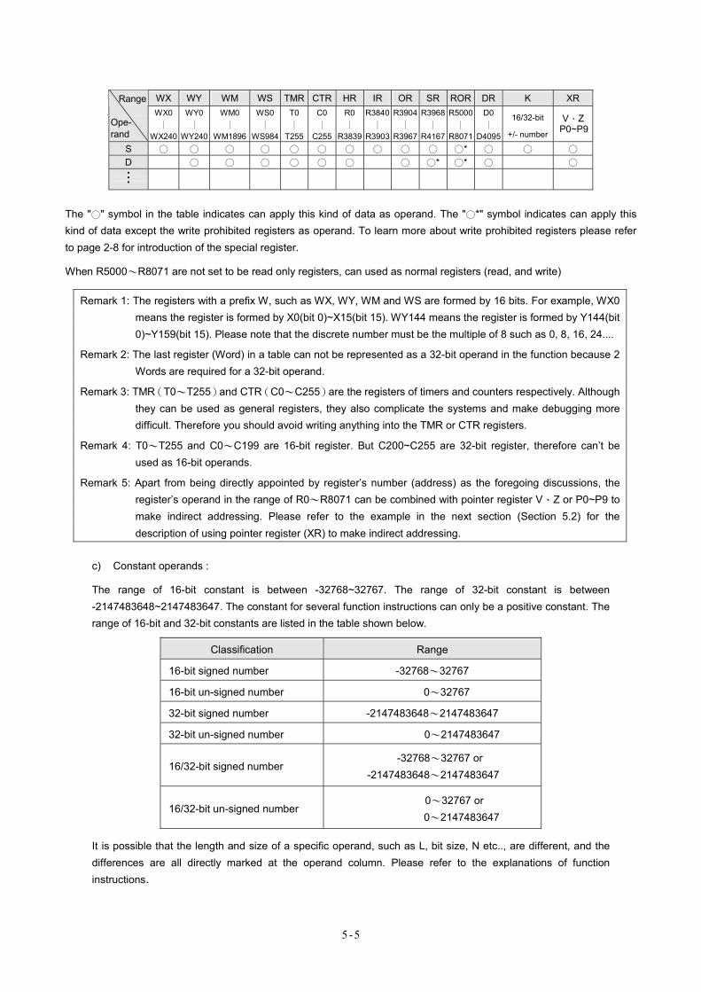
5-5
WX WY WM WS TMR CTR HR IR OR SR ROR DR K XR Range
Ope- rand
WX0 ∣
WX240
WY0 ∣
WY240
WM0 ∣
WM1896
WS0 ∣
WS984
T0∣
T255
C0∣
C255
R0∣
R3839
R3840∣
R3903
R3904∣
R3967
R3968∣
R4167
R5000∣
R8071
D0∣
D4095
16/32-bit
+/- number
V、ZP0~P9
S ○ ○ ○ ○ ○ ○ ○ ○ ○ ○ ○* ○ ○ ○ D ○ ○ ○ ○ ○ ○ ○ ○* ○* ○ ○ • • •
The "○" symbol in the table indicates can apply this kind of data as operand. The "○*" symbol indicates can apply this kind of data except the write prohibited registers as operand. To learn more about write prohibited registers please refer to page 2-8 for introduction of the special register.
When R5000~R8071 are not set to be read only registers, can used as normal registers (read, and write)
Remark 1: The registers with a prefix W, such as WX, WY, WM and WS are formed by 16 bits. For example, WX0 means the register is formed by X0(bit 0)~X15(bit 15). WY144 means the register is formed by Y144(bit 0)~Y159(bit 15). Please note that the discrete number must be the multiple of 8 such as 0, 8, 16, 24....
Remark 2: The last register (Word) in a table can not be represented as a 32-bit operand in the function because 2 Words are required for a 32-bit operand.
Remark 3: TMR(T0~T255)and CTR(C0~C255)are the registers of timers and counters respectively. Although they can be used as general registers, they also complicate the systems and make debugging more difficult. Therefore you should avoid writing anything into the TMR or CTR registers.
Remark 4: T0~T255 and C0~C199 are 16-bit register. But C200~C255 are 32-bit register, therefore can’t be used as 16-bit operands.
Remark 5: Apart from being directly appointed by register’s number (address) as the foregoing discussions, the register’s operand in the range of R0~R8071 can be combined with pointer register V、Z or P0~P9 to make indirect addressing. Please refer to the example in the next section (Section 5.2) for the description of using pointer register (XR) to make indirect addressing.
c) Constant operands :
The range of 16-bit constant is between -32768~32767. The range of 32-bit constant is between -2147483648~2147483647. The constant for several function instructions can only be a positive constant. The range of 16-bit and 32-bit constants are listed in the table shown below.
Classification Range
16-bit signed number -32768~32767
16-bit un-signed number 0~32767
32-bit signed number -2147483648~2147483647
32-bit un-signed number 0~2147483647
16/32-bit signed number -32768~32767 or
-2147483648~2147483647
16/32-bit un-signed number 0~32767 or 0~2147483647
It is possible that the length and size of a specific operand, such as L, bit size, N etc.., are different, and the differences are all directly marked at the operand column. Please refer to the explanations of function instructions.
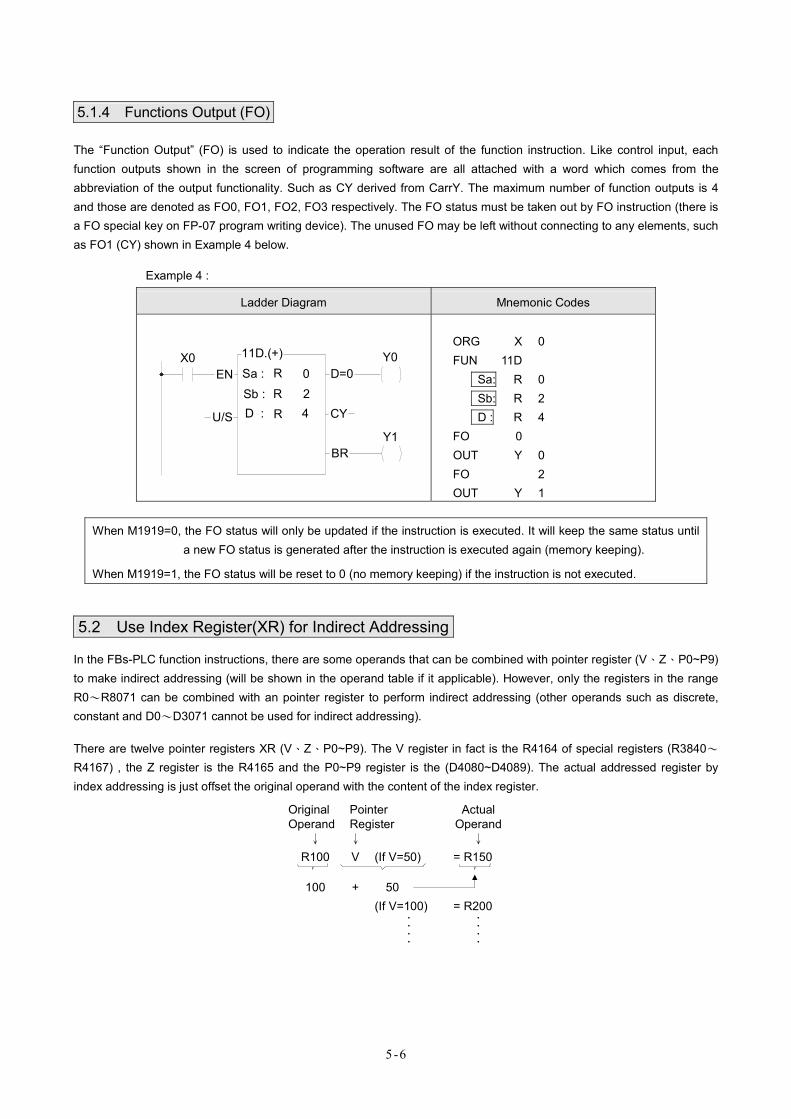
5-6
5.1.4 Functions Output (FO)
The “Function Output” (FO) is used to indicate the operation result of the function instruction. Like control input, each function outputs shown in the screen of programming software are all attached with a word which comes from the abbreviation of the output functionality. Such as CY derived from CarrY. The maximum number of function outputs is 4 and those are denoted as FO0, FO1, FO2, FO3 respectively. The FO status must be taken out by FO instruction (there is a FO special key on FP-07 program writing device). The unused FO may be left without connecting to any elements, such as FO1 (CY) shown in Example 4 below.
Example 4 :
Ladder Diagram Mnemonic Codes
X0EN D=0
CY
BR
11D.(+) Y0
Y1
Sa :
Sb :D :
R
RR
024U/S
ORG X 0 FUN 11D Sa: R 0 Sb: R 2 D : R 4 FO 0 OUT Y 0 FO 2 OUT Y 1
When M1919=0, the FO status will only be updated if the instruction is executed. It will keep the same status until a new FO status is generated after the instruction is executed again (memory keeping).
When M1919=1, the FO status will be reset to 0 (no memory keeping) if the instruction is not executed.
5.2 Use Index Register(XR) for Indirect Addressing
In the FBs-PLC function instructions, there are some operands that can be combined with pointer register (V、Z、P0~P9) to make indirect addressing (will be shown in the operand table if it applicable). However, only the registers in the range R0~R8071 can be combined with an pointer register to perform indirect addressing (other operands such as discrete, constant and D0~D3071 cannot be used for indirect addressing).
There are twelve pointer registers XR (V、Z、P0~P9). The V register in fact is the R4164 of special registers (R3840~
R4167) , the Z register is the R4165 and the P0~P9 register is the (D4080~D4089). The actual addressed register by index addressing is just offset the original operand with the content of the index register.
Original Operand
↓
Pointer Register ↓
ActualOperand
↓ R100 V (If V=50) = R150
100 + 50 (If V=100) = R200
• • • •
• • • •
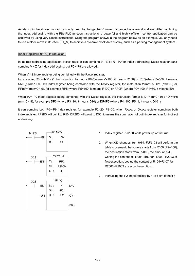
5-7
As shown in the above diagram, you only need to change the V value to change the operand address. After combining the index addressing with the FBs-PLC function instructions, a powerful and highly efficient control application can be achieved by using very simple instructions. Using the program shown in the diagram below as an example, you only need to use a block move instruction (BT_M) to achieve a dynamic block data display, such as a parking management system.
Index Register(P0~P9) Introduction
In indirect addressing application, Rxxxx register can combine V、Z & P0~P9 for index addressing; Dxxxx register can't combine V、Z for index addressing, but P0~P9 are allowed.
When V、Z index register being combined with the Rxxxx register, for example, R0 with V、Z, the instruction format is R0V(where V=100, it means R100) or R0Z(where Z=500, it means R500); when P0~P9 index register being combined with the Rxxxx register, the instruction format is RPn (n=0~9) or RPmPn (m,n=0~9), for example RP5 (where P5=100, it means R100) or RP0P1(where P0= 100, P1=50, it means150).
When P0~P9 index register being combined with the Dxxxx register, the instruction format is DPn (n=0~9) or DPmPn (m,n=0~9), for example DP3 (where P3=10, it means D10) or DP4P5 (where P4=100, P5=1, it means D101).
It can combine both P0~P9 index register, for example P2=20, P3=30, when Rxxxx or Dxxxx register combines both index register, RP2P3 will point to R50, DP2P3 will point to D50, it means the summation of both index register for indirect addressing.
EN
EN
ENX23
X23
M1924
L : 4
11P.(+)
P2
4
P2
Sa :
D :
Sb :
103.BT_M
RP3
R2000
Ts :
Td :
08.MOV
100
P2D :
S :
U/S
BR
CY
D=0
1. Index register P2=100 while power up or first run. 2. When X23 changes from 0 1, FUN103 will perform the
table movement, the source starts from R100 (P2=100), the destination starts from R2000, the amount is 4. Coping the content of R100~R103 for R2000~R2003 at first execution, coping the content of R104~R107 for R2000~R2003 at second execution…
3. Increasing the P2 index register by 4 to point to next 4
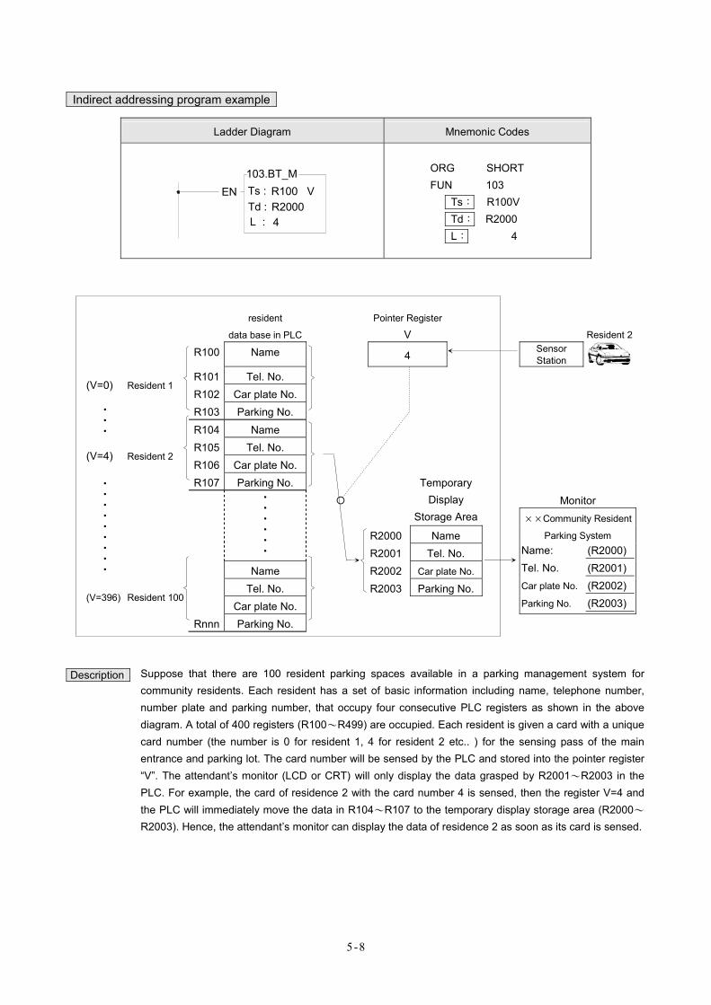
5-8
Indirect addressing program example
Ladder Diagram Mnemonic Codes
103.BT_MTs :Td :
EN R100 VR20004L :
ORG SHORT FUN 103
Ts: R100V Td: R2000 L: 4
resident
data base in PLC
Pointer Register
V
R100 Name 4 Sensor Station
R101 Tel. No.
Resident 2
(V=0) Resident 1 R102 Car plate No.
R103 Parking No. ˙ ˙ ˙ R104 Name
R105 Tel. No. (V=4) Resident 2
R106 Car plate No. R107 Parking No. Monitor
Temporary Display
Storage Area R2000 Name
××Community Resident
Parking System
˙ ˙ ˙ ˙ ˙ ˙ R2001 Tel. No. Name: (R2000)
˙ ˙ ˙ ˙ ˙ ˙ ˙ ˙ ˙ Name R2002 Car plate No. Tel. No. (R2001)
Tel. No. R2003 Parking No. Car plate No. (R2002)(V=396) Resident 100
Car plate No. Parking No. (R2003)
Rnnn Parking No.
Description Suppose that there are 100 resident parking spaces available in a parking management system for community residents. Each resident has a set of basic information including name, telephone number, number plate and parking number, that occupy four consecutive PLC registers as shown in the above diagram. A total of 400 registers (R100~R499) are occupied. Each resident is given a card with a unique card number (the number is 0 for resident 1, 4 for resident 2 etc.. ) for the sensing pass of the main entrance and parking lot. The card number will be sensed by the PLC and stored into the pointer register “V”. The attendant’s monitor (LCD or CRT) will only display the data grasped by R2001~R2003 in the PLC. For example, the card of residence 2 with the card number 4 is sensed, then the register V=4 and the PLC will immediately move the data in R104~R107 to the temporary display storage area (R2000~
R2003). Hence, the attendant’s monitor can display the data of residence 2 as soon as its card is sensed.
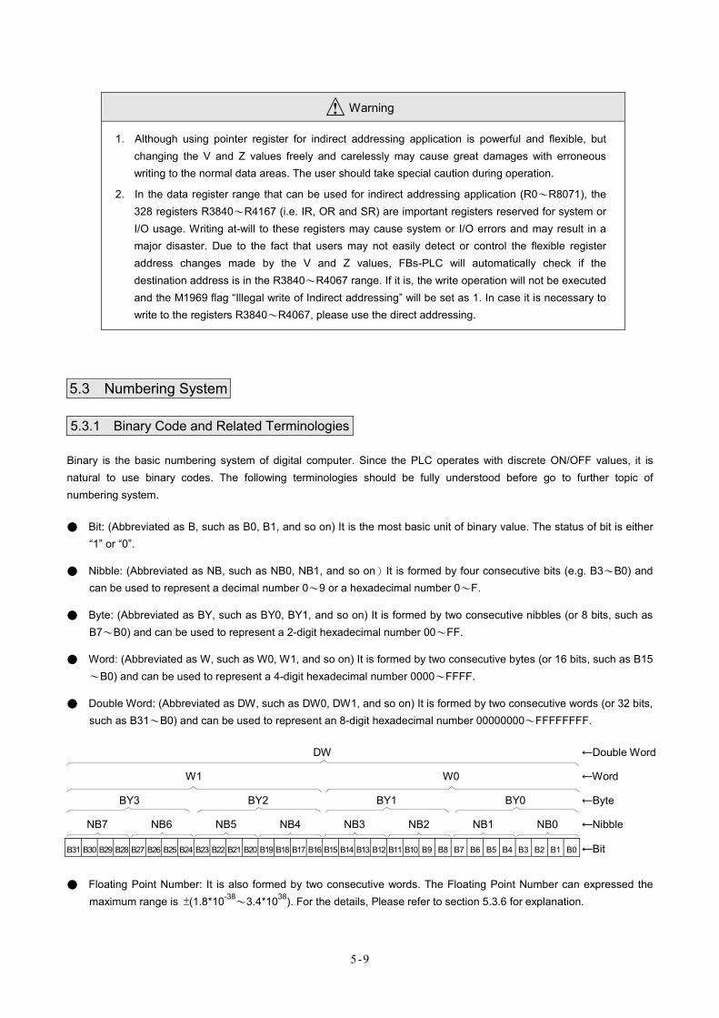
5-9
Warning
1. Although using pointer register for indirect addressing application is powerful and flexible, but changing the V and Z values freely and carelessly may cause great damages with erroneous writing to the normal data areas. The user should take special caution during operation.
2. In the data register range that can be used for indirect addressing application (R0~R8071), the 328 registers R3840~R4167 (i.e. IR, OR and SR) are important registers reserved for system or I/O usage. Writing at-will to these registers may cause system or I/O errors and may result in a major disaster. Due to the fact that users may not easily detect or control the flexible register address changes made by the V and Z values, FBs-PLC will automatically check if the destination address is in the R3840~R4067 range. If it is, the write operation will not be executed and the M1969 flag “Illegal write of Indirect addressing” will be set as 1. In case it is necessary to write to the registers R3840~R4067, please use the direct addressing.
5.3 Numbering System
5.3.1 Binary Code and Related Terminologies
Binary is the basic numbering system of digital computer. Since the PLC operates with discrete ON/OFF values, it is natural to use binary codes. The following terminologies should be fully understood before go to further topic of numbering system.
● Bit: (Abbreviated as B, such as B0, B1, and so on) It is the most basic unit of binary value. The status of bit is either “1” or “0”.
● Nibble: (Abbreviated as NB, such as NB0, NB1, and so on)It is formed by four consecutive bits (e.g. B3~B0) and can be used to represent a decimal number 0~9 or a hexadecimal number 0~F.
● Byte: (Abbreviated as BY, such as BY0, BY1, and so on) It is formed by two consecutive nibbles (or 8 bits, such as B7~B0) and can be used to represent a 2-digit hexadecimal number 00~FF.
● Word: (Abbreviated as W, such as W0, W1, and so on) It is formed by two consecutive bytes (or 16 bits, such as B15~B0) and can be used to represent a 4-digit hexadecimal number 0000~FFFF.
● Double Word: (Abbreviated as DW, such as DW0, DW1, and so on) It is formed by two consecutive words (or 32 bits, such as B31~B0) and can be used to represent an 8-digit hexadecimal number 00000000~FFFFFFFF.
DW ←Double Word
W1 W0 ←Word
BY3 BY2 BY1 BY0 ←Byte
NB7 NB6 NB5 NB4 NB3 NB2 NB1 NB0 ←Nibble
B31 B30 B29 B28 B27 B26 B25 B24 B23 B22 B21 B20 B19 B18 B17 B16 B15 B14 B13 B12 B11 B10 B9 B8 B7 B6 B5 B4 B3 B2 B1 B0 ←Bit
● Floating Point Number: It is also formed by two consecutive words. The Floating Point Number can expressed the maximum range is ±(1.8*10-38
~3.4*1038). For the details, Please refer to section 5.3.6 for explanation.
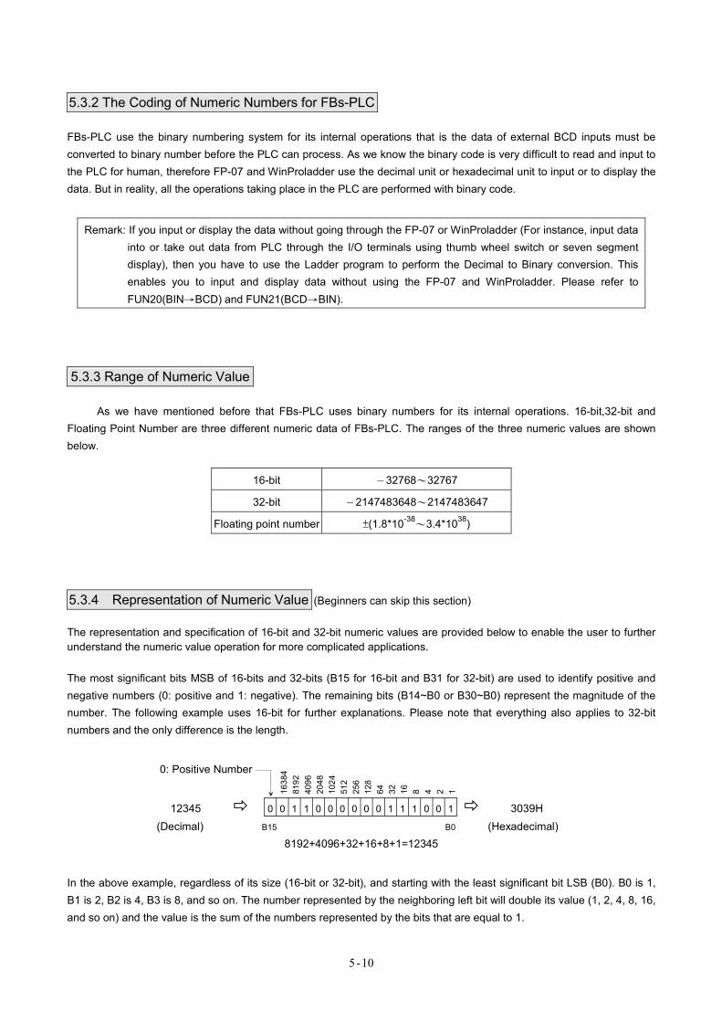
5-10
5.3.2 The Coding of Numeric Numbers for FBs-PLC
FBs-PLC use the binary numbering system for its internal operations that is the data of external BCD inputs must be converted to binary number before the PLC can process. As we know the binary code is very difficult to read and input to the PLC for human, therefore FP-07 and WinProladder use the decimal unit or hexadecimal unit to input or to display the data. But in reality, all the operations taking place in the PLC are performed with binary code.
Remark: If you input or display the data without going through the FP-07 or WinProladder (For instance, input data into or take out data from PLC through the I/O terminals using thumb wheel switch or seven segment display), then you have to use the Ladder program to perform the Decimal to Binary conversion. This enables you to input and display data without using the FP-07 and WinProladder. Please refer to FUN20(BIN→BCD) and FUN21(BCD→BIN).
5.3.3 Range of Numeric Value
As we have mentioned before that FBs-PLC uses binary numbers for its internal operations. 16-bit,32-bit and Floating Point Number are three different numeric data of FBs-PLC. The ranges of the three numeric values are shown below.
16-bit −32768~32767
32-bit −2147483648~2147483647
Floating point number ±(1.8*10-38~3.4*1038)
5.3.4 Representation of Numeric Value (Beginners can skip this section)
The representation and specification of 16-bit and 32-bit numeric values are provided below to enable the user to further understand the numeric value operation for more complicated applications.
The most significant bits MSB of 16-bits and 32-bits (B15 for 16-bit and B31 for 32-bit) are used to identify positive and negative numbers (0: positive and 1: negative). The remaining bits (B14~B0 or B30~B0) represent the magnitude of the number. The following example uses 16-bit for further explanations. Please note that everything also applies to 32-bit numbers and the only difference is the length.
0: Positive Number
1638
4 81
92
4096
20
48
1024
51
2 25
6 12
8 64
32
16
8 4 2 1
12345 0 0 1 1 0 0 0 0 0 0 1 1 1 0 0 1 3039H (Decimal) B15 B0 (Hexadecimal)
8192+4096+32+16+8+1=12345
In the above example, regardless of its size (16-bit or 32-bit), and starting with the least significant bit LSB (B0). B0 is 1, B1 is 2, B2 is 4, B3 is 8, and so on. The number represented by the neighboring left bit will double its value (1, 2, 4, 8, 16, and so on) and the value is the sum of the numbers represented by the bits that are equal to 1.
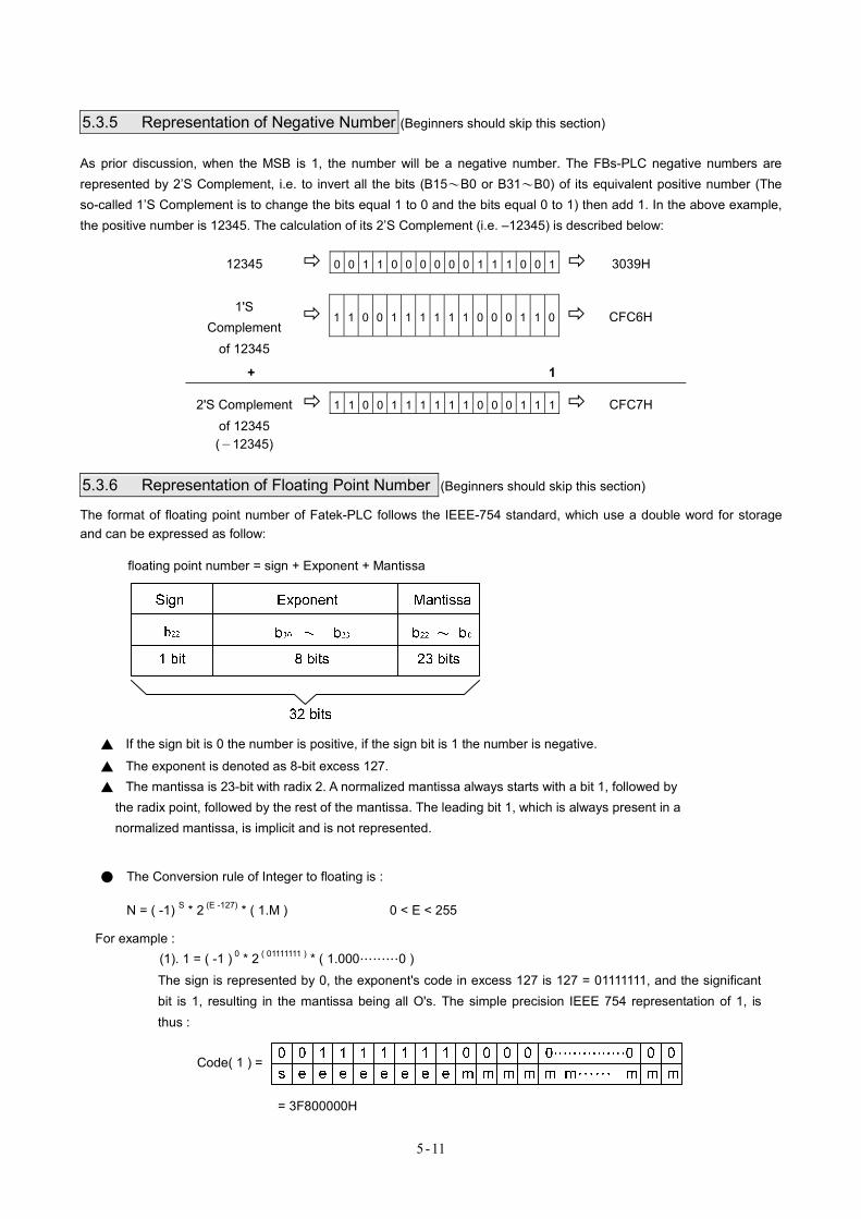
5-11
5.3.5 Representation of Negative Number (Beginners should skip this section)
As prior discussion, when the MSB is 1, the number will be a negative number. The FBs-PLC negative numbers are represented by 2’S Complement, i.e. to invert all the bits (B15~B0 or B31~B0) of its equivalent positive number (The so-called 1’S Complement is to change the bits equal 1 to 0 and the bits equal 0 to 1) then add 1. In the above example, the positive number is 12345. The calculation of its 2’S Complement (i.e. –12345) is described below:
12345 0 0 1 1 0 0 0 0 0 0 1 1 1 0 0 1 3039H
1'S Complement
1 1 0 0 1 1 1 1 1 1 0 0 0 1 1 0 CFC6H
of 12345
+ 1
2'S Complement 1 1 0 0 1 1 1 1 1 1 0 0 0 1 1 1 CFC7H of 12345 (−12345)
5.3.6 Representation of Floating Point Number (Beginners should skip this section)
The format of floating point number of Fatek-PLC follows the IEEE-754 standard, which use a double word for storage and can be expressed as follow:
floating point number = sign + Exponent + Mantissa
▲ If the sign bit is 0 the number is positive, if the sign bit is 1 the number is negative.
▲ The exponent is denoted as 8-bit excess 127. ▲ The mantissa is 23-bit with radix 2. A normalized mantissa always starts with a bit 1, followed by
the radix point, followed by the rest of the mantissa. The leading bit 1, which is always present in a normalized mantissa, is implicit and is not represented.
● The Conversion rule of Integer to floating is :
N = ( -1) S * 2 (E -127) * ( 1.M ) 0 < E < 255 For example : (1). 1 = ( -1 ) 0 * 2 ( 01111111 ) * ( 1.000………0 )
The sign is represented by 0, the exponent's code in excess 127 is 127 = 01111111, and the significant bit is 1, resulting in the mantissa being all O's. The simple precision IEEE 754 representation of 1, is thus :
= 3F800000H
Code( 1 ) =
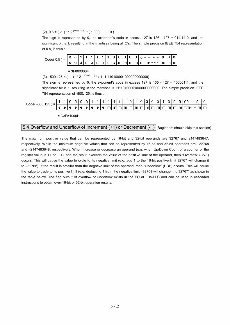
5-12
(2). 0.5 = ( -1 ) 0 * 2 ( 01111110 ) * ( 1.000………0 ) The sign is represented by 0, the exponent's code in excess 127 is 126 - 127 = 01111110, and the significant bit is 1, resulting in the mantissa being all O's. The simple precision IEEE 754 representation of 0.5, is thus :
= 3F000000H (3). -500.125 = ( -1 ) 1 * 2 ( 10000111 ) * ( 1. 11110100001000000000000)
The sign is represented by 0, the exponent's code in excess 127 is 135 - 127 = 10000111, and the significant bit is 1, resulting in the mantissa is 11110100001000000000000. The simple precision IEEE 754 representation of -500.125, is thus :
= C3FA1000H
5.4 Overflow and Underflow of Increment (+1) or Decrement (-1) (Beginners should skip this section)
The maximum positive value that can be represented by 16-bit and 32-bit operands are 32767 and 2147483647, respectively. While the minimum negative values that can be represented by 16-bit and 32-bit operands are –32768 and –2147483648, respectively. When increase or decrease an operand (e.g. when Up/Down Count of a counter or the register value is +1 or −1), and the result exceeds the value of the positive limit of the operand, then “Overflow” (OVF) occurs. This will cause the value to cycle to its negative limit (e.g. add 1 to the 16-bit positive limit 32767 will change it to –32768). If the result is smaller than the negative limit of the operand, then “Underflow” (UDF) occurs. This will cause the value to cycle to its positive limit (e.g. deducting 1 from the negative limit –32768 will change it to 32767) as shown in the table below. The flag output of overflow or underflow exists in the FO of FBs-PLC and can be used in cascaded instructions to obtain over 16-bit or 32-bit operation results.
Code( 0.5 ) =
Code( -500.125 ) =
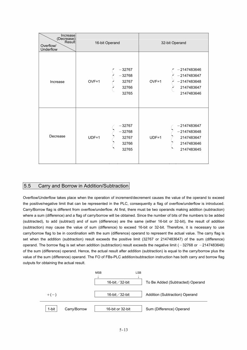
5-13
Increase
(Decrease) Result
Overflow/ Underflow
16-bit Operand 32-bit Operand
Increase OVF=1
−32767 −32768 32767 32766 32765
OVF=1
−2147483646 −2147483647 −2147483648 2147483647 2147483646
Decrease UDF=1
−32767 −32768 32767 32766 32765
UDF=1
−2147483647 −2147483648 2147483647 2147483646 2147483645
5.5 Carry and Borrow in Addition/Subtraction
Overflow/Underflow takes place when the operation of increment/decrement causes the value of the operand to exceed the positive/negative limit that can be represented in the PLC, consequently a flag of overflow/underflow is introduced. Carry/Borrow flag is different from overflow/underflow. At first, there must be two operands making addition (subtraction) where a sum (difference) and a flag of carry/borrow will be obtained. Since the number of bits of the numbers to be added (subtracted), to add (subtract) and of sum (difference) are the same (either 16-bit or 32-bit), the result of addition (subtraction) may cause the value of sum (difference) to exceed 16-bit or 32-bit. Therefore, it is necessary to use carry/borrow flag to be in coordination with the sum (difference) operand to represent the actual value. The carry flag is set when the addition (subtraction) result exceeds the positive limit (32767 or 2147483647) of the sum (difference) operand. The borrow flag is set when addition (subtraction) result exceeds the negative limit (−32768 or −2147483648) of the sum (difference) operand. Hence, the actual result after addition (subtraction) is equal to the carry/borrow plus the value of the sum (difference) operand. The FO of FBs-PLC addition/subtraction instruction has both carry and borrow flag outputs for obtaining the actual result.
MSB ↓
LSB↓
16-bit/32-bit To Be Added (Subtracted) Operand +(−) 16-bit/32-bit Addition (Subtraction) Operand
1-bit Carry/Borrow 16-bit or 32-bit Sum (Difference) Operand
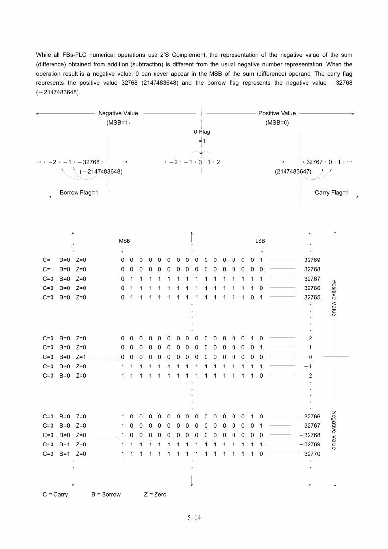
5-14
While all FBs-PLC numerical operations use 2’S Complement, the representation of the negative value of the sum (difference) obtained from addition (subtraction) is different from the usual negative number representation. When the operation result is a negative value, 0 can never appear in the MSB of the sum (difference) operand. The carry flag represents the positive value 32768 (2147483648) and the borrow flag represents the negative value −32768 (−2147483648).
Negative Value (MSB=1)
Positive Value (MSB=0)
0 Flag
=1
,−2,−1,−32768, (−2147483648)
,−2,−1,0,1,2,
,32767,0,1,
(2147483647)
Borrow Flag=1 Carry Flag=1
MSB
↓
LSB
↓
C=1 B=0 Z=0 0 0 0 0 0 0 0 0 0 0 0 0 0 0 0 1 32769 C=1 B=0 Z=0 0 0 0 0 0 0 0 0 0 0 0 0 0 0 0 0 32768 C=0 B=0 Z=0 0 1 1 1 1 1 1 1 1 1 1 1 1 1 1 1 32767 C=0 B=0 Z=0 0 1 1 1 1 1 1 1 1 1 1 1 1 1 1 0 32766 C=0 B=0 Z=0 0 1 1 1 1 1 1 1 1 1 1 1 1 1 0 1 32765
C=0 B=0 Z=0 0 0 0 0 0 0 0 0 0 0 0 0 0 0 1 0 2 C=0 B=0 Z=0 0 0 0 0 0 0 0 0 0 0 0 0 0 0 0 1 1 C=0 B=0 Z=1 0 0 0 0 0 0 0 0 0 0 0 0 0 0 0 0 0
Positive V
alue
C=0 B=0 Z=0 1 1 1 1 1 1 1 1 1 1 1 1 1 1 1 1 −1 C=0 B=0 Z=0 1 1 1 1 1 1 1 1 1 1 1 1 1 1 1 0 −2
C=0 B=0 Z=0 1 0 0 0 0 0 0 0 0 0 0 0 0 0 1 0 −32766 C=0 B=0 Z=0 1 0 0 0 0 0 0 0 0 0 0 0 0 0 0 1 −32767 C=0 B=0 Z=0 1 0 0 0 0 0 0 0 0 0 0 0 0 0 0 0 −32768 C=0 B=1 Z=0 1 1 1 1 1 1 1 1 1 1 1 1 1 1 1 1 −32769 C=0 B=1 Z=0 1 1 1 1 1 1 1 1 1 1 1 1 1 1 1 0 −32770
Negative V
alue
C = Carry B = Borrow Z = Zero
6-1
Chapter 6 Basic Function Instruction
T …………………………………6-2
C …………………………………6-5
SET …………………………………6-8
RST …………………………………6-10
0:MC …………………………………6-12
1:MCE …………………………………6-14
2:SKP …………………………………6-15
3:SKPE …………………………………6-17
4:DIFU …………………………………6-18
5:DIFD …………………………………6-19
6:BSHF …………………………………6-20
7:UDCTR…………………………………6-21
8:MOV …………………………………6-23
9:MOV/ …………………………………6-24
10:TOGG …………………………………6-25
11:(+) …………………………………6-26
12:(-) …………………………………6-27
13:(*) …………………………………6-28
14:(/) …………………………………6-30
15:(+1) …………………………………6-32
16:(-1) …………………………………6-33
17:CMP …………………………………6-34
18:AND …………………………………6-35
19:OR …………………………………6-36
20:→BCD…………………………………6-37
21:→BIN …………………………………6-38
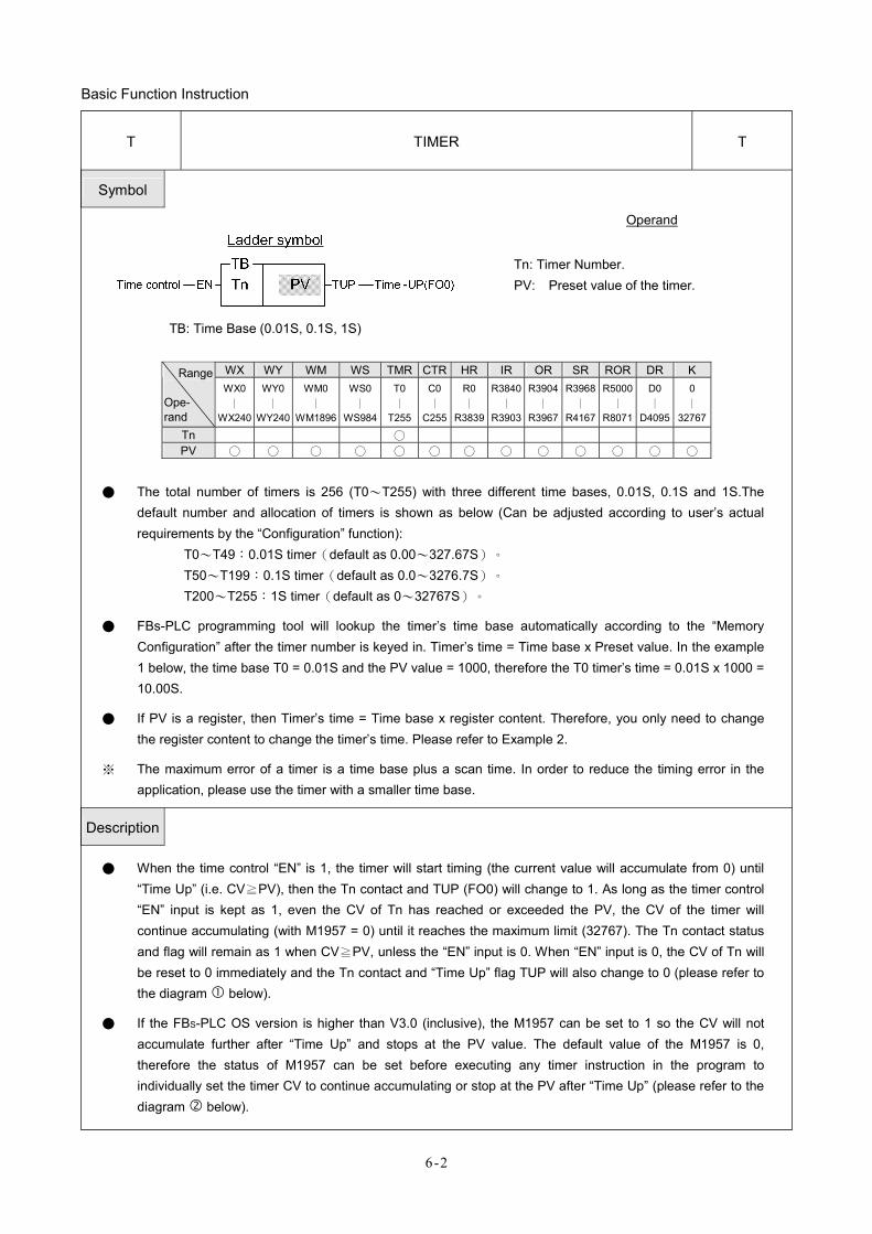
Basic Function Instruction
6-2
T TIMER T
Symbol
TB: Time Base (0.01S, 0.1S, 1S)
Operand
Tn: Timer Number. PV: Preset value of the timer.
WX WY WM WS TMR CTR HR IR OR SR ROR DR K Range
Ope- rand
WX0 ∣
WX240
WY0 ∣
WY240
WM0 ∣
WM1896
WS0∣
WS984
T0 ∣
T255
C0∣
C255
R0 ∣
R3839
R3840∣
R3903
R3904∣
R3967
R3968∣
R4167
R5000 ∣
R8071
D0 ∣
D4095
0 ∣
32767
Tn ○ PV ○ ○ ○ ○ ○ ○ ○ ○ ○ ○ ○ ○ ○
● The total number of timers is 256 (T0~T255) with three different time bases, 0.01S, 0.1S and 1S.The
default number and allocation of timers is shown as below (Can be adjusted according to user’s actual requirements by the “Configuration” function):
T0~T49:0.01S timer(default as 0.00~327.67S)。 T50~T199:0.1S timer(default as 0.0~3276.7S)。 T200~T255:1S timer(default as 0~32767S)。
● FBs-PLC programming tool will lookup the timer’s time base automatically according to the “Memory Configuration” after the timer number is keyed in. Timer’s time = Time base x Preset value. In the example 1 below, the time base T0 = 0.01S and the PV value = 1000, therefore the T0 timer’s time = 0.01S x 1000 = 10.00S.
● If PV is a register, then Timer’s time = Time base x register content. Therefore, you only need to change the register content to change the timer’s time. Please refer to Example 2.
※ The maximum error of a timer is a time base plus a scan time. In order to reduce the timing error in the application, please use the timer with a smaller time base.
Description
● When the time control “EN” is 1, the timer will start timing (the current value will accumulate from 0) until “Time Up” (i.e. CV≧PV), then the Tn contact and TUP (FO0) will change to 1. As long as the timer control “EN” input is kept as 1, even the CV of Tn has reached or exceeded the PV, the CV of the timer will continue accumulating (with M1957 = 0) until it reaches the maximum limit (32767). The Tn contact status and flag will remain as 1 when CV≧PV, unless the “EN” input is 0. When “EN” input is 0, the CV of Tn will be reset to 0 immediately and the Tn contact and “Time Up” flag TUP will also change to 0 (please refer to the diagram below).
● If the FBS-PLC OS version is higher than V3.0 (inclusive), the M1957 can be set to 1 so the CV will not accumulate further after “Time Up” and stops at the PV value. The default value of the M1957 is 0, therefore the status of M1957 can be set before executing any timer instruction in the program to individually set the timer CV to continue accumulating or stop at the PV after “Time Up” (please refer to the diagram below).
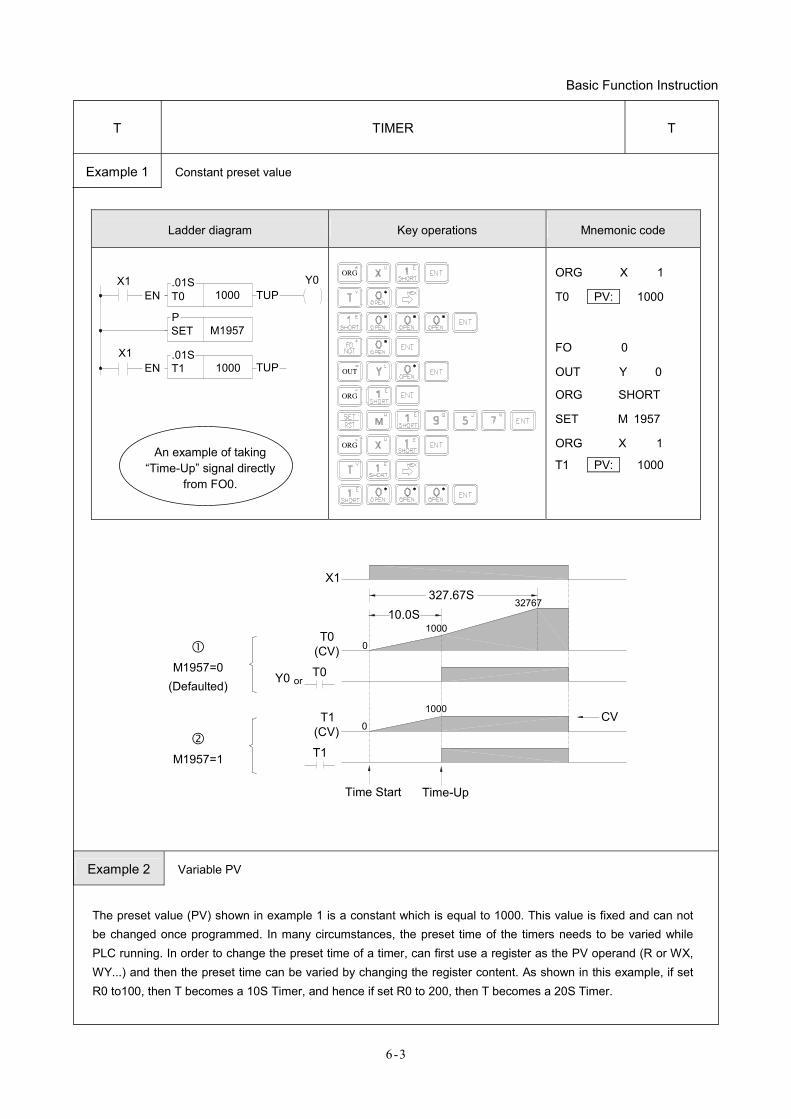
Basic Function Instruction
6-3
Ladder diagram Key operations Mnemonic code
P
X1
EN
EN
.01S
.01S
T0 1000
SET M1957
T1 1000
X1 Y0TUP
TUP
An example of taking “Time-Up” signal directly
from FO0.
ORG
ORG
OUT
ORG ORG X 1
T0 PV: 1000
FO 0
OUT Y 0
ORG SHORT
SET M 1957
ORG X 1
T1 PV: 1000
M1957=0
(Defaulted)
M1957=1
X1
T0(CV)
Y0 T0
T1
T1(CV)
or
1000
0
0
32767
1000CV
Time Start Time-Up
10.0S327.67S
Example 2 Variable PV
The preset value (PV) shown in example 1 is a constant which is equal to 1000. This value is fixed and can not be changed once programmed. In many circumstances, the preset time of the timers needs to be varied while PLC running. In order to change the preset time of a timer, can first use a register as the PV operand (R or WX, WY...) and then the preset time can be varied by changing the register content. As shown in this example, if set R0 to100, then T becomes a 10S Timer, and hence if set R0 to 200, then T becomes a 20S Timer.
T TIMER T
Example 1 Constant preset value
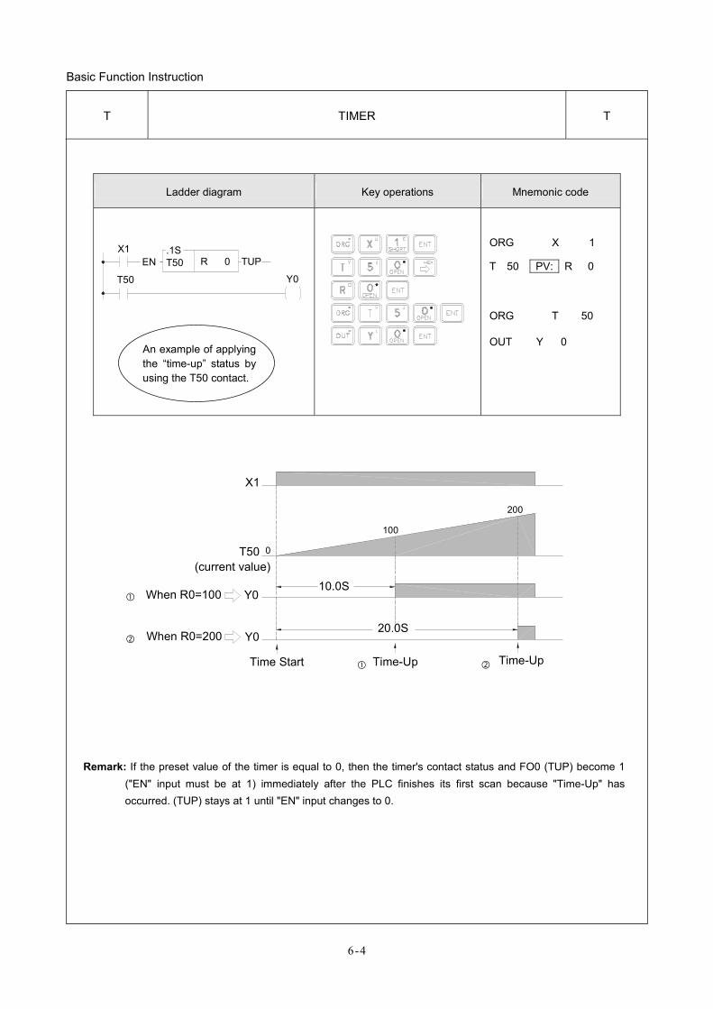
Basic Function Instruction
6-4
T TIMER T
Ladder diagram Key operations Mnemonic code
X1EN TUP
.1S
Y0T50
T50 R 0
An example of applying the “time-up” status by using the T50 contact.
ORG X 1
T 50 PV: R 0
ORG T 50
OUT Y 0
X1
T50
When R0=100
When R0=200
Time Start Time-Up Time-Up
(current value)10.0S
20.0S
Y0
Y0
0
100
200
Remark: If the preset value of the timer is equal to 0, then the timer's contact status and FO0 (TUP) become 1
("EN" input must be at 1) immediately after the PLC finishes its first scan because "Time-Up" has occurred. (TUP) stays at 1 until "EN" input changes to 0.
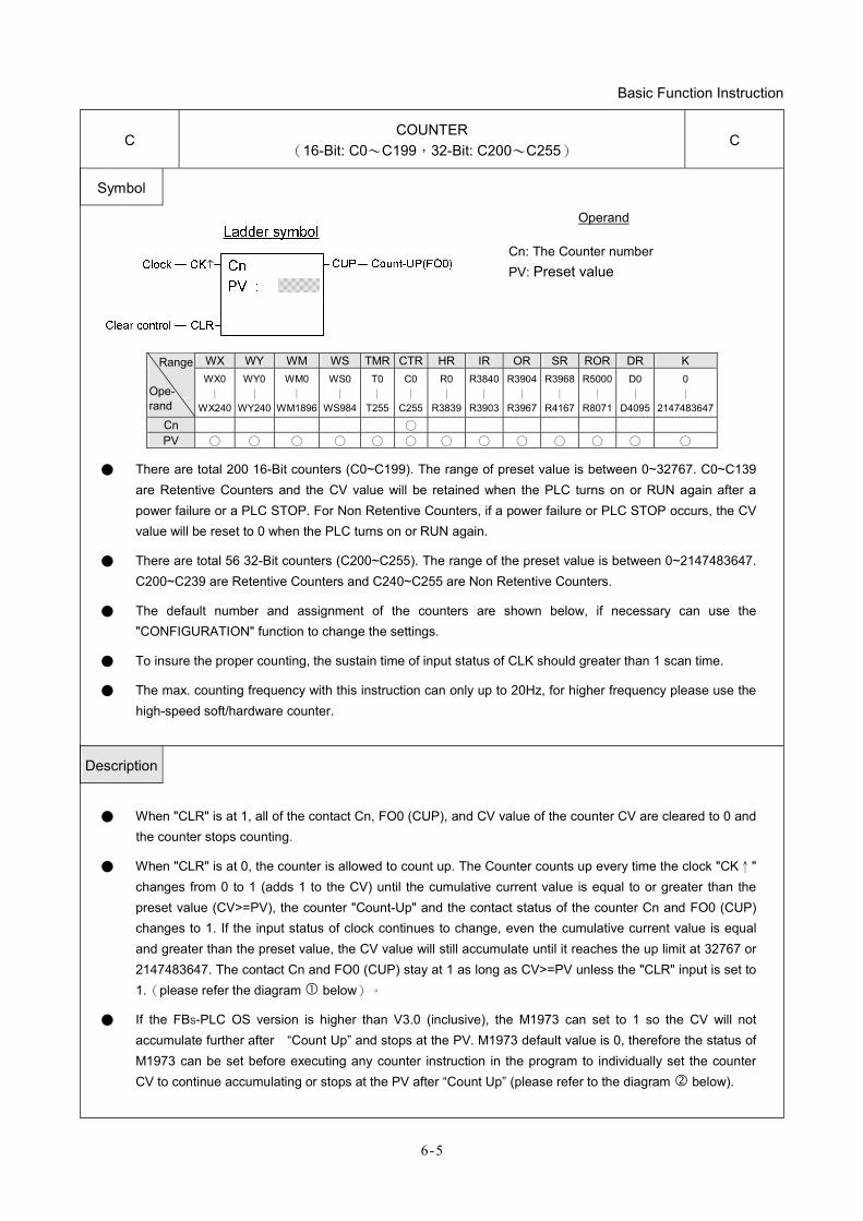
Basic Function Instruction
6-5
C COUNTER
(16-Bit: C0~C199,32-Bit: C200~C255) C
Symbol
Operand Cn: The Counter number PV: Preset value
WX WY WM WS TMR CTR HR IR OR SR ROR DR K Range
Ope- rand
WX0 ∣
WX240
WY0∣
WY240
WM0 ∣
WM1896
WS0 ∣
WS984
T0∣
T255
C0∣
C255
R0 ∣
R3839
R3840∣
R3903
R3904∣
R3967
R3968∣
R4167
R5000 ∣
R8071
D0 ∣
D4095
0 ∣
2147483647
Cn ○ PV ○ ○ ○ ○ ○ ○ ○ ○ ○ ○ ○ ○ ○
● There are total 200 16-Bit counters (C0~C199). The range of preset value is between 0~32767. C0~C139 are Retentive Counters and the CV value will be retained when the PLC turns on or RUN again after a power failure or a PLC STOP. For Non Retentive Counters, if a power failure or PLC STOP occurs, the CV value will be reset to 0 when the PLC turns on or RUN again.
● There are total 56 32-Bit counters (C200~C255). The range of the preset value is between 0~2147483647. C200~C239 are Retentive Counters and C240~C255 are Non Retentive Counters.
● The default number and assignment of the counters are shown below, if necessary can use the "CONFIGURATION" function to change the settings.
● To insure the proper counting, the sustain time of input status of CLK should greater than 1 scan time.
● The max. counting frequency with this instruction can only up to 20Hz, for higher frequency please use the high-speed soft/hardware counter.
Description
● When "CLR" is at 1, all of the contact Cn, FO0 (CUP), and CV value of the counter CV are cleared to 0 and
the counter stops counting.
● When "CLR" is at 0, the counter is allowed to count up. The Counter counts up every time the clock "CK↑" changes from 0 to 1 (adds 1 to the CV) until the cumulative current value is equal to or greater than the preset value (CV>=PV), the counter "Count-Up" and the contact status of the counter Cn and FO0 (CUP) changes to 1. If the input status of clock continues to change, even the cumulative current value is equal and greater than the preset value, the CV value will still accumulate until it reaches the up limit at 32767 or 2147483647. The contact Cn and FO0 (CUP) stay at 1 as long as CV>=PV unless the "CLR" input is set to 1.(please refer the diagram below)。
● If the FBS-PLC OS version is higher than V3.0 (inclusive), the M1973 can set to 1 so the CV will not accumulate further after “Count Up” and stops at the PV. M1973 default value is 0, therefore the status of M1973 can be set before executing any counter instruction in the program to individually set the counter CV to continue accumulating or stops at the PV after “Count Up” (please refer to the diagram below).
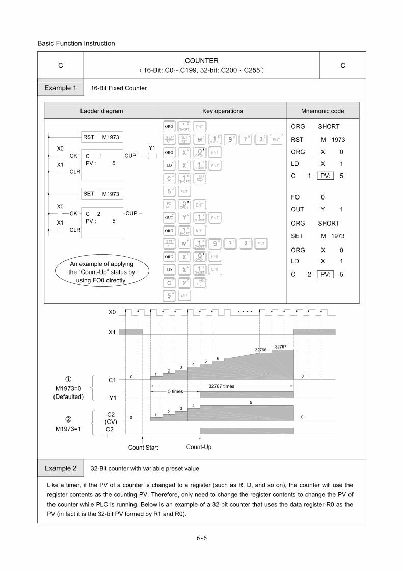
Basic Function Instruction
6-6
C COUNTER
(16-Bit: C0~C199, 32-bit: C200~C255) C
Example 1 16-Bit Fixed Counter
Ladder diagram Key operations Mnemonic code
C 1PV :
X0CK
SET M1973
CUPY1
RST M1973
X1CLR
5
C 2PV :
X0
X1CLR
5CK CUP
An example of applying the “Count-Up” status by
using FO0 directly.
ORG
LD
ORG
OUT
LD
ORG
ORG ORG SHORT
RST M 1973
ORG X 0
LD X 1
C 1 PV: 5
FO 0
OUT Y 1
ORG SHORT
SET M 1973
ORG X 0
LD X 1
C 2 PV: 5
M1973=0
(Defaulted)
M1973=1
Count Start Count-Up
X0
X1
C1
Y1
C2
C2(CV)
0
0
12
34
56
12
34
3276632767
0
0
5
5 times32767 times
Example 2 32-Bit counter with variable preset value Like a timer, if the PV of a counter is changed to a register (such as R, D, and so on), the counter will use the register contents as the counting PV. Therefore, only need to change the register contents to change the PV of the counter while PLC is running. Below is an example of a 32-bit counter that uses the data register R0 as the PV (in fact it is the 32-bit PV formed by R1 and R0).
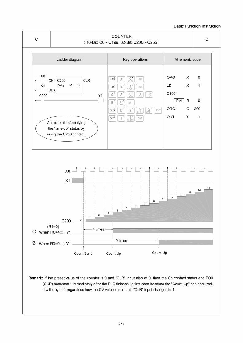
Basic Function Instruction
6-7
C COUNTER
(16-Bit: C0~C199, 32-Bit: C200~C255) C
Ladder diagram Key operations Mnemonic code
PV : R 0
X0CK
C200 Y1
X1CLR
C200 CLR
An example of applying the “time-up” status by
using the C200 contact.
ORG
OUT
LD
ORG
ORG X 0
LD X 1
C200
PV: R 0
ORG C 200
OUT Y 1
X0
X1
C200(R1=0)
When R0=4
When R0=9
Y1
Y1
Count Start Count-Up
4 times
9 times
Count-Up
01
23
45
67
89
1011
1213
14
Remark: If the preset value of the counter is 0 and "CLR" input also at 0, then the Cn contact status and FO0 (CUP) becomes 1 immediately after the PLC finishes its first scan because the "Count-Up" has occurred. It will stay at 1 regardless how the CV value varies until "CLR" input changes to 1.
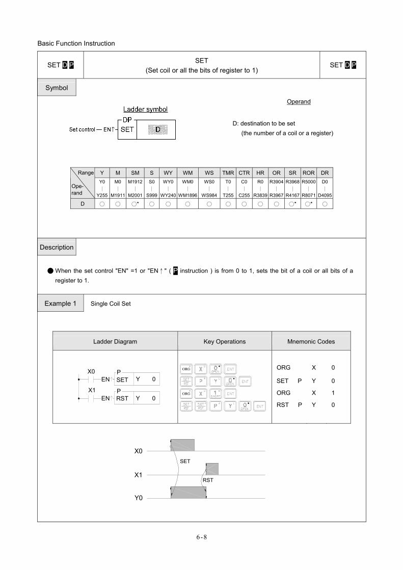
Basic Function Instruction
6-8
SET D P SET (Set coil or all the bits of register to 1)
SET D P
Symbol
Operand
D: destination to be set (the number of a coil or a register)
Y M SM S WY WM WS TMR CTR HR OR SR ROR DR Range
Ope- rand
Y0 ∣
Y255
M0∣
M1911
M1912 ∣
M2001
S0 ∣
S999
WY0∣
WY240
WM0∣
WM1896
WS0 ∣
WS984
T0∣
T255
C0∣
C255
R0∣
R3839
R3904∣
R3967
R3968 ∣
R4167
R5000 ∣
R8071
D0 ∣
D4095
D ○ ○ ○* ○ ○ ○ ○ ○ ○ ○ ○ ○* ○* ○
Description
● When the set control "EN" =1 or "EN↑" ( P instruction ) is from 0 to 1, sets the bit of a coil or all bits of a
register to 1.
Example 1 Single Coil Set
Ladder Diagram Key Operations Mnemonic Codes
X1
X0EN
EN
P
P
SET
RST
Y 0
Y 0
ORG
ORG
ORG
SET P
ORG
RST P
X
Y
X
Y
0
0
1
0
X0
X1
Y0
SET
RST
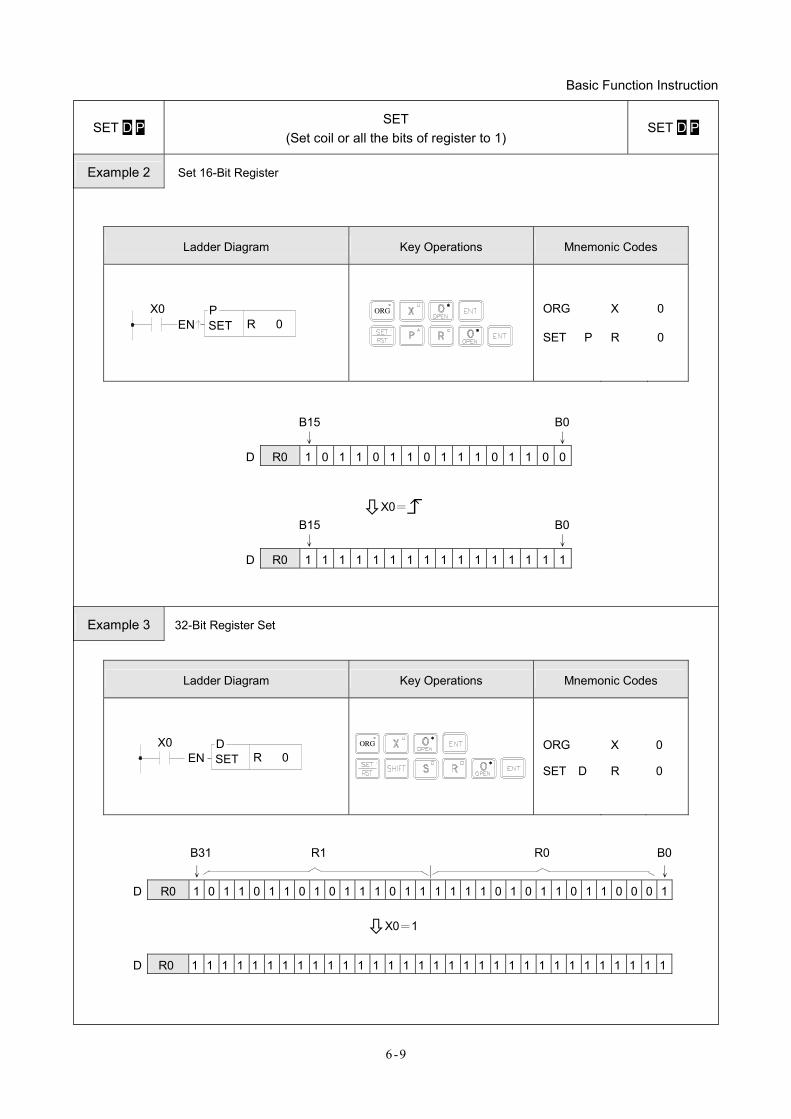
Basic Function Instruction
6-9
SET D P SET
(Set coil or all the bits of register to 1) SET D P
Example 2 Set 16-Bit Register
Ladder Diagram Key Operations Mnemonic Codes
PSET
X0EN R 0
ORG
ORG
SET P
X
R
0
0
B15 B0 ↓ ↓
D R0 1 0 1 1 0 1 1 0 1 1 1 0 1 1 0 0
X0= B15 B0 ↓ ↓
D R0 1 1 1 1 1 1 1 1 1 1 1 1 1 1 1 1
Example 3 32-Bit Register Set
Ladder Diagram Key Operations Mnemonic Codes
SET R 0X0
END
ORG
ORG
SET D
X
R
0
0
B31 R1 R0 B0 ↓ ∣ ↓
D R0 1 0 1 1 0 1 1 0 1 0 1 1 1 0 1 1 1 1 1 1 0 1 0 1 1 0 1 1 0 0 0 1
X0=1
D R0 1 1 1 1 1 1 1 1 1 1 1 1 1 1 1 1 1 1 1 1 1 1 1 1 1 1 1 1 1 1 1 1
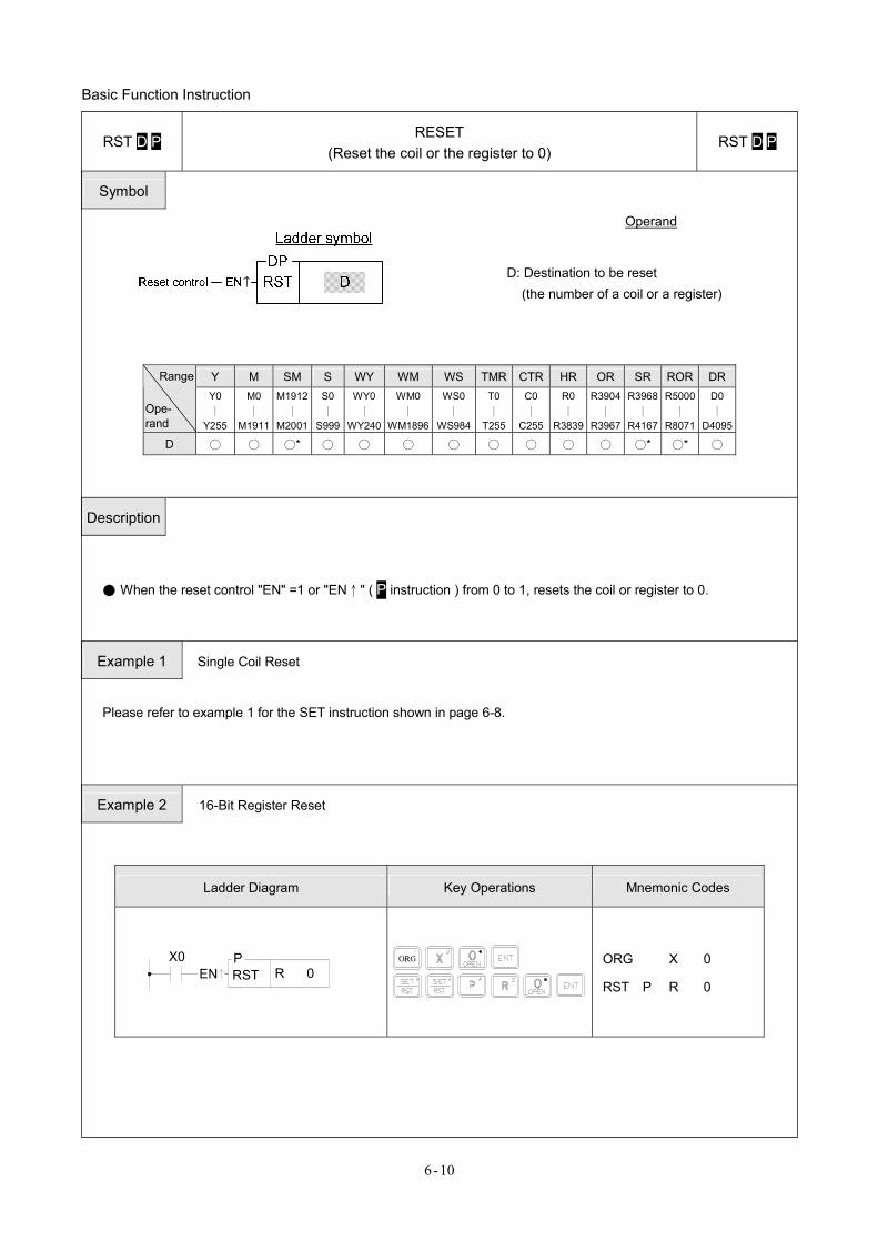
Basic Function Instruction
6-10
RST D P RESET (Reset the coil or the register to 0)
RST D P
Symbol
Operand
D: Destination to be reset (the number of a coil or a register)
Y M SM S WY WM WS TMR CTR HR OR SR ROR DR Range
Ope- rand
Y0 ∣
Y255
M0 ∣
M1911
M1912 ∣
M2001
S0 ∣
S999
WY0∣
WY240
WM0 ∣
WM1896
WS0∣
WS984
T0 ∣
T255
C0 ∣
C255
R0 ∣
R3839
R3904 ∣
R3967
R3968 ∣
R4167
R5000 ∣
R8071
D0 ∣
D4095
D ○ ○ ○* ○ ○ ○ ○ ○ ○ ○ ○ ○* ○* ○
Description
● When the reset control "EN" =1 or "EN↑" ( P instruction ) from 0 to 1, resets the coil or register to 0.
Example 1 Single Coil Reset
Please refer to example 1 for the SET instruction shown in page 6-8.
Example 2 16-Bit Register Reset
Ladder Diagram Key Operations Mnemonic Codes
PR 0
X0EN RST
ORG ORG X 0
RST P R 0
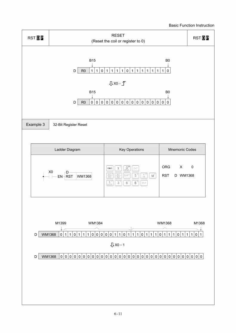
Basic Function Instruction
6-11
RST D P RESET (Reset the coil or register to 0)
RST D P
B15 B0 ↓ ↓
D R0 1 1 0 1 1 1 1 0 1 1 1 1 1 1 1 0
X0=
B15 B0 ↓ ↓
D R0 0 0 0 0 0 0 0 0 0 0 0 0 0 0 0 0
Example 3 32-Bit Register Reset
Ladder Diagram Key Operations Mnemonic Codes
DX0EN RST WM1368
ORG
ORG X 0
RST D WM1368
M1399 WM1384 WM1368 M1368 ↓ ∣ ↓
D WM1368 0 1 1 0 1 1 1 0 0 0 0 0 1 1 0 1 1 1 0 1 1 1 0 1 1 1 0 1 1 1 0 1
X0=1
D WM1368 0 0 0 0 0 0 0 0 0 0 0 0 0 0 0 0 0 0 0 0 0 0 0 0 0 0 0 0 0 0 0 0
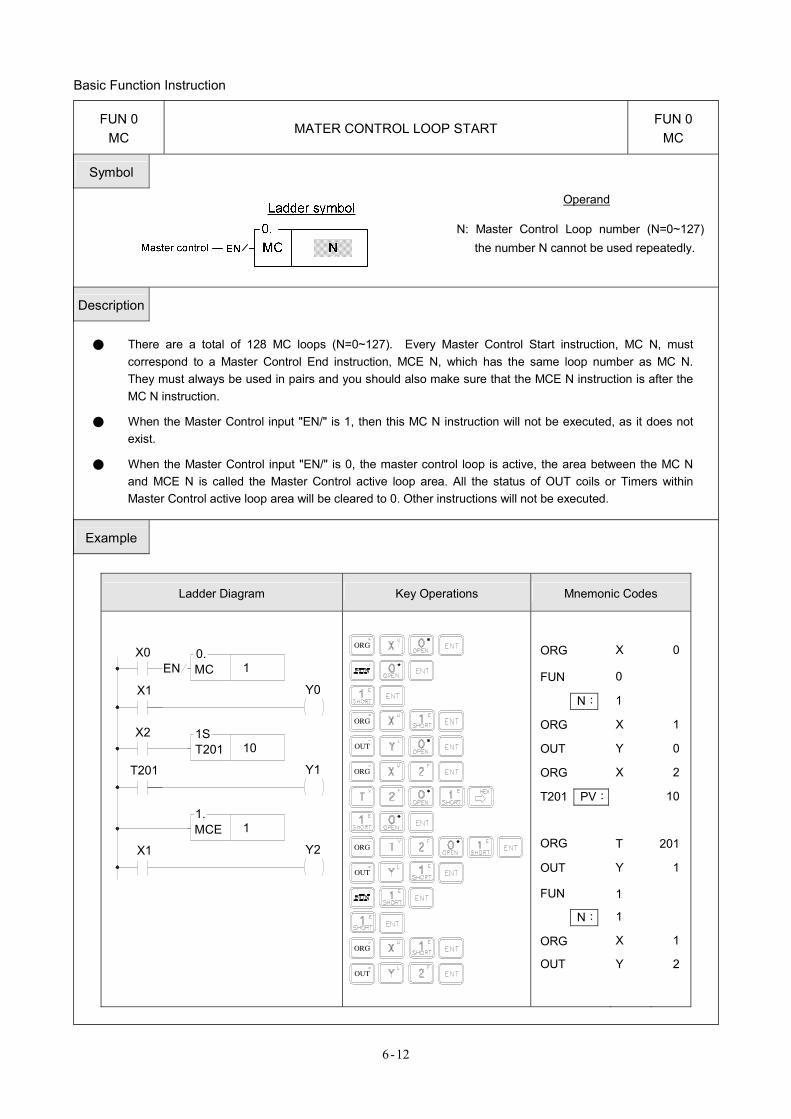
Basic Function Instruction
6-12
FUN 0 MC
MATER CONTROL LOOP START FUN 0
MC
Symbol
Operand N: Master Control Loop number (N=0~127)
the number N cannot be used repeatedly.
Description
● There are a total of 128 MC loops (N=0~127). Every Master Control Start instruction, MC N, must correspond to a Master Control End instruction, MCE N, which has the same loop number as MC N. They must always be used in pairs and you should also make sure that the MCE N instruction is after the MC N instruction.
● When the Master Control input "EN/" is 1, then this MC N instruction will not be executed, as it does not exist.
● When the Master Control input "EN/" is 0, the master control loop is active, the area between the MC N and MCE N is called the Master Control active loop area. All the status of OUT coils or Timers within Master Control active loop area will be cleared to 0. Other instructions will not be executed.
Example
Ladder Diagram Key Operations Mnemonic Codes
0.MC 1
X0EN
X1
1ST201 10
X2
T201
1.MCE 1
X1 Y2
Y1
Y0
OUT
ORG
ORG
OUT
ORG
ORG
OUT
ORG
ORG
FUN
N:
ORG
OUT
ORG
T201 PV:
ORG
OUT
FUN
N:
ORG
OUT
X
0
1
X
Y
X
T
Y
1
1
X
Y
0
1
0
2
10
201
1
1
2
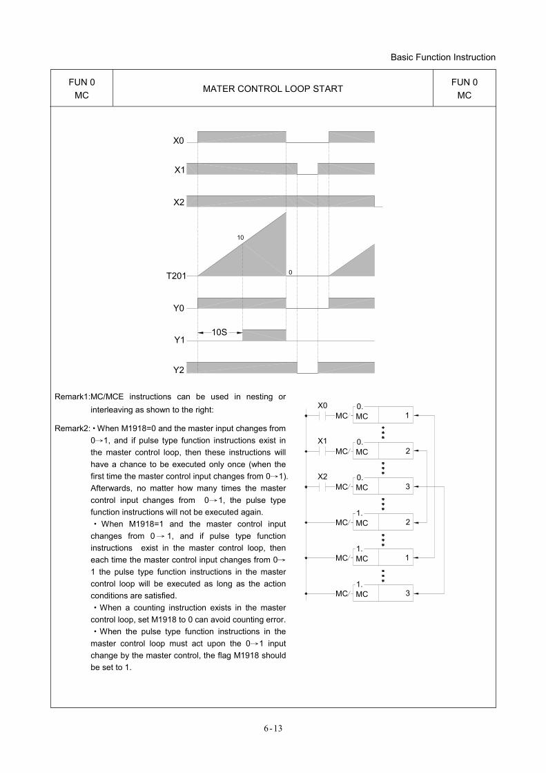
Basic Function Instruction
6-13
FUN 0 MC
MATER CONTROL LOOP START FUN 0
MC
X0
X1
X2
T201
Y0
Y1
Y2
10S
10
0
Remark1:MC/MCE instructions can be used in nesting or interleaving as shown to the right:
Remark2:•When M1918=0 and the master input changes from 0→1, and if pulse type function instructions exist in the master control loop, then these instructions will have a chance to be executed only once (when the first time the master control input changes from 0→1). Afterwards, no matter how many times the master control input changes from 0→1, the pulse type function instructions will not be executed again. •When M1918=1 and the master control input changes from 0 → 1, and if pulse type function instructions exist in the master control loop, then each time the master control input changes from 0→1 the pulse type function instructions in the master control loop will be executed as long as the action conditions are satisfied. •When a counting instruction exists in the master control loop, set M1918 to 0 can avoid counting error. •When the pulse type function instructions in the master control loop must act upon the 0→1 input change by the master control, the flag M1918 should be set to 1.
0.MC 1
X0MC
0.MC 2
X1
0.MC 3
X2
1.MC 2
1.MC 1
1.MC 3
MC
MC
MC
MC
MC
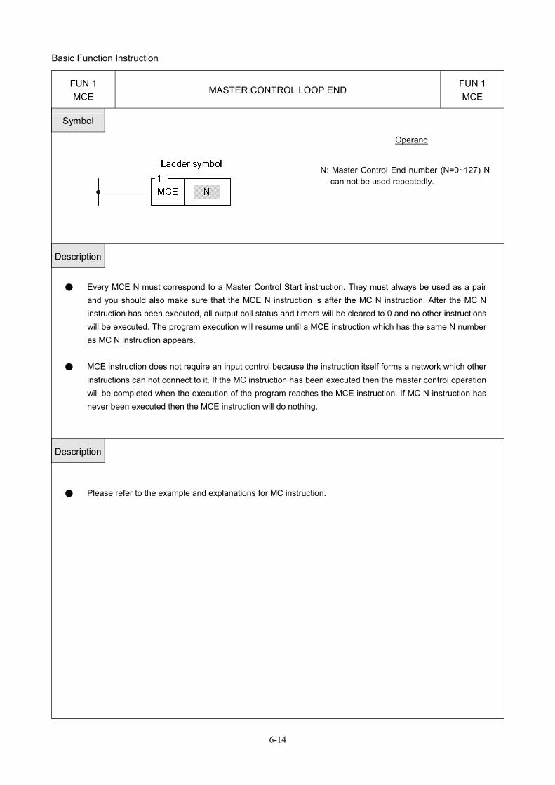
Basic Function Instruction
6-14
FUN 1 MCE
MASTER CONTROL LOOP END FUN 1 MCE
Symbol
Operand
N: Master Control End number (N=0~127) N can not be used repeatedly.
Description
● Every MCE N must correspond to a Master Control Start instruction. They must always be used as a pair and you should also make sure that the MCE N instruction is after the MC N instruction. After the MC N instruction has been executed, all output coil status and timers will be cleared to 0 and no other instructions will be executed. The program execution will resume until a MCE instruction which has the same N number as MC N instruction appears.
● MCE instruction does not require an input control because the instruction itself forms a network which other
instructions can not connect to it. If the MC instruction has been executed then the master control operation will be completed when the execution of the program reaches the MCE instruction. If MC N instruction has never been executed then the MCE instruction will do nothing.
Description
● Please refer to the example and explanations for MC instruction.
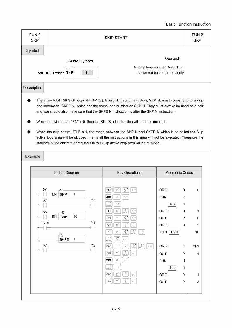
Basic Function Instruction
6-15
FUN 2 SKP
SKIP START FUN 2 SKP
Symbol
Operand
N: Skip loop number (N=0~127), N can not be used repeatedly.
Description
● There are total 128 SKP loops (N=0~127). Every skip start instruction, SKP N, must correspond to a skip end instruction, SKPE N, which has the same loop number as SKP N. They must always be used as a pair and you should also make sure that the SKPE N instruction is after the SKP N instruction.
● When the skip control "EN" is 0, then the Skip Start instruction will not be executed.
● When the skip control "EN" is 1, the range between the SKP N and SKPE N which is so called the Skip
active loop area will be skipped, that is all the instructions in this area will not be executed. Therefore the statuses of the discrete or registers in this Skip active loop area will be retained.
Example
Ladder Diagram Key Operations Mnemonic Codes
1X0
Y0X1
1ST201 10
X2
Y1T201
1
Y2X1
2.
3.
EN
EN
SKP
SKPE
ORG
OUT
OUT
ORG
OUT
ORG
ORG
ORG
ORG
FUN
N:
ORG
OUT
ORG
T201 PV:
ORG
OUT
FUN
N:
ORG
OUT
X
2
1
X
Y
X
T
Y
3
1
X
Y
0
1
0
2
10
201
1
1
2
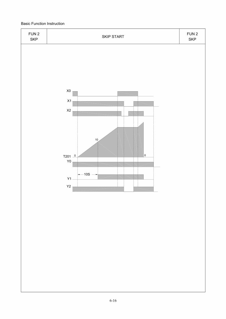
Basic Function Instruction
6-16
FUN 2 SKP
SKIP START FUN 2 SKP
Y2
Y1
Y0T201
10S
X0
X1
X2
0
10
0
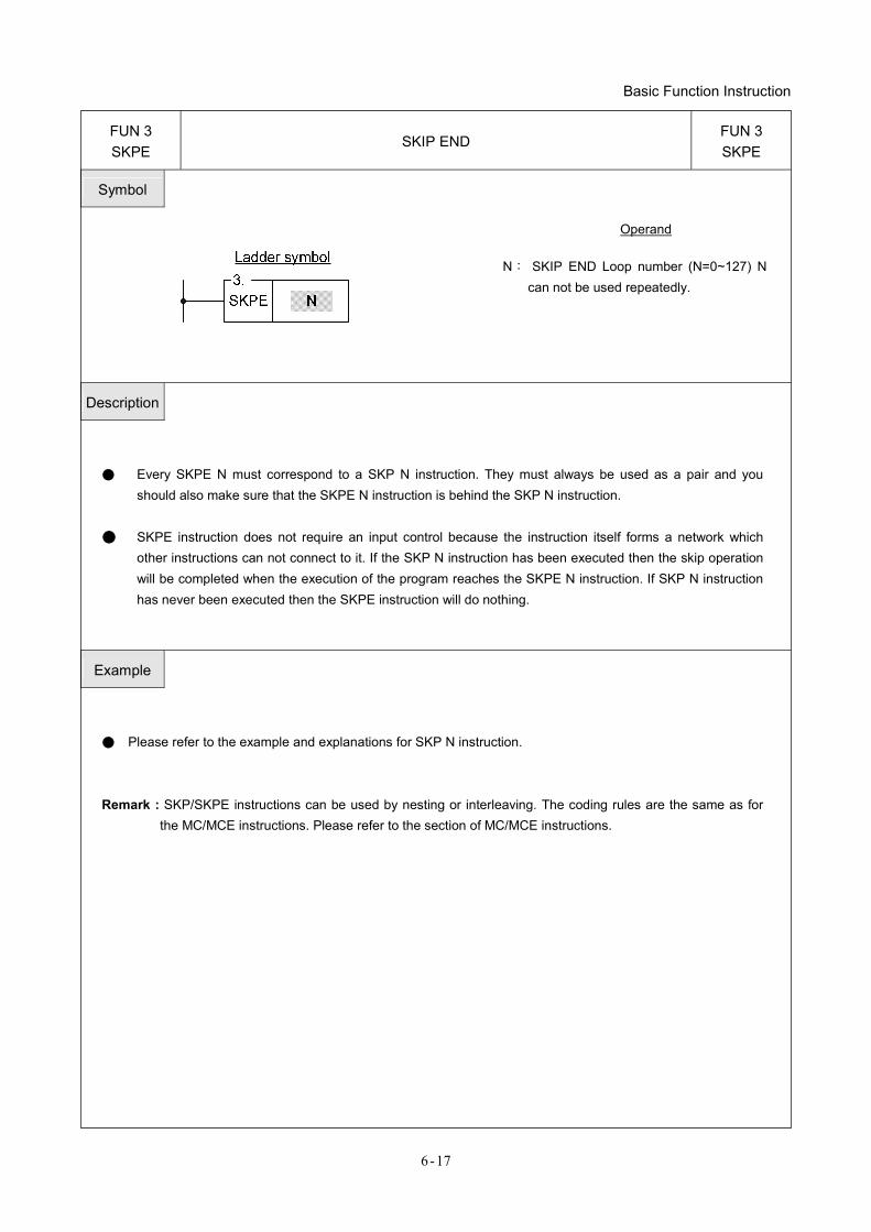
Basic Function Instruction
6-17
FUN 3 SKPE
SKIP END FUN 3 SKPE
Symbol
Operand N: SKIP END Loop number (N=0~127) N
can not be used repeatedly.
Description
● Every SKPE N must correspond to a SKP N instruction. They must always be used as a pair and you should also make sure that the SKPE N instruction is behind the SKP N instruction.
● SKPE instruction does not require an input control because the instruction itself forms a network which
other instructions can not connect to it. If the SKP N instruction has been executed then the skip operation will be completed when the execution of the program reaches the SKPE N instruction. If SKP N instruction has never been executed then the SKPE instruction will do nothing.
Example
● Please refer to the example and explanations for SKP N instruction.
Remark : SKP/SKPE instructions can be used by nesting or interleaving. The coding rules are the same as for the MC/MCE instructions. Please refer to the section of MC/MCE instructions.
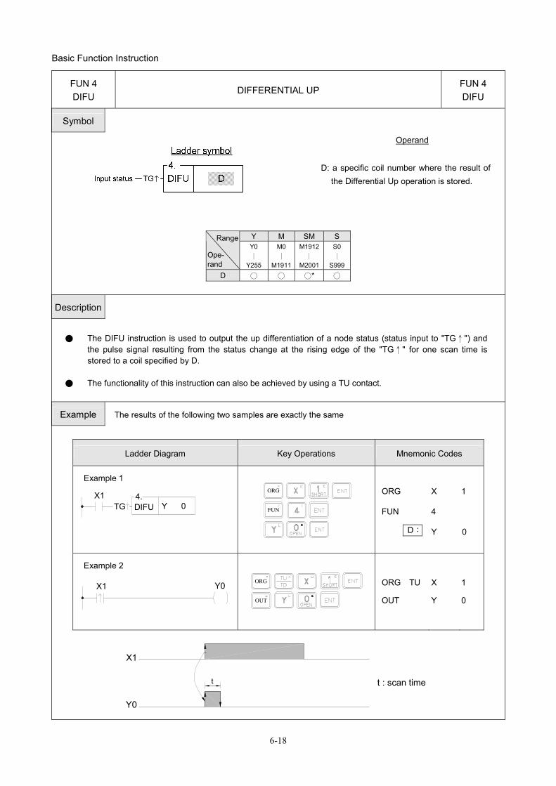
Basic Function Instruction
6-18
FUN 4 DIFU
DIFFERENTIAL UP FUN 4 DIFU
Symbol
Operand
D: a specific coil number where the result of the Differential Up operation is stored.
Y M SM S Range
Ope- rand
Y0 ∣
Y255
M0 ∣
M1911
M1912∣
M2001
S0 ∣
S999D ○ ○ ○* ○
Description
● The DIFU instruction is used to output the up differentiation of a node status (status input to "TG↑") and
the pulse signal resulting from the status change at the rising edge of the "TG↑" for one scan time is stored to a coil specified by D.
● The functionality of this instruction can also be achieved by using a TU contact.
Example The results of the following two samples are exactly the same
Ladder Diagram Key Operations Mnemonic Codes
Example 1
X1TG
4.DIFU Y 0
ORG
FUN
ORG
FUN
D:
X
4
Y
1
0
Example 2
Y0X1OUT
ORG
ORG TU
OUT
X
Y
1
0
X1
Y0
t t : scan time
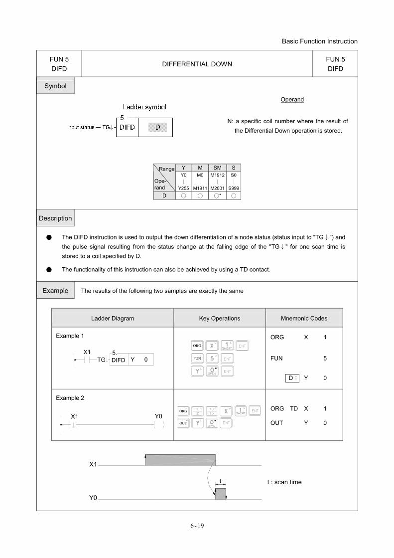
Basic Function Instruction
6 -19
FUN 5 DIFD
DIFFERENTIAL DOWN FUN 5 DIFD
Symbol
Operand
N: a specific coil number where the result of the Differential Down operation is stored.
Y M SM SRange
Ope- rand
Y0 ∣
Y255
M0∣
M1911
M1912∣
M2001
S0∣
S999D ○ ○ ○* ○
Description
● The DIFD instruction is used to output the down differentiation of a node status (status input to "TG↓") and the pulse signal resulting from the status change at the falling edge of the "TG↓" for one scan time is stored to a coil specified by D.
● The functionality of this instruction can also be achieved by using a TD contact.
Example The results of the following two samples are exactly the same
Ladder Diagram Key Operations Mnemonic Codes
Example 1
Y 0X1
TG5.DIFD
ORG
FUN
ORG X 1
FUN 5
D: Y 0
Example 2
Y0X1
ORG
OUT
ORG TD X 1
OUT Y 0
X1
Y0
t : scan timet
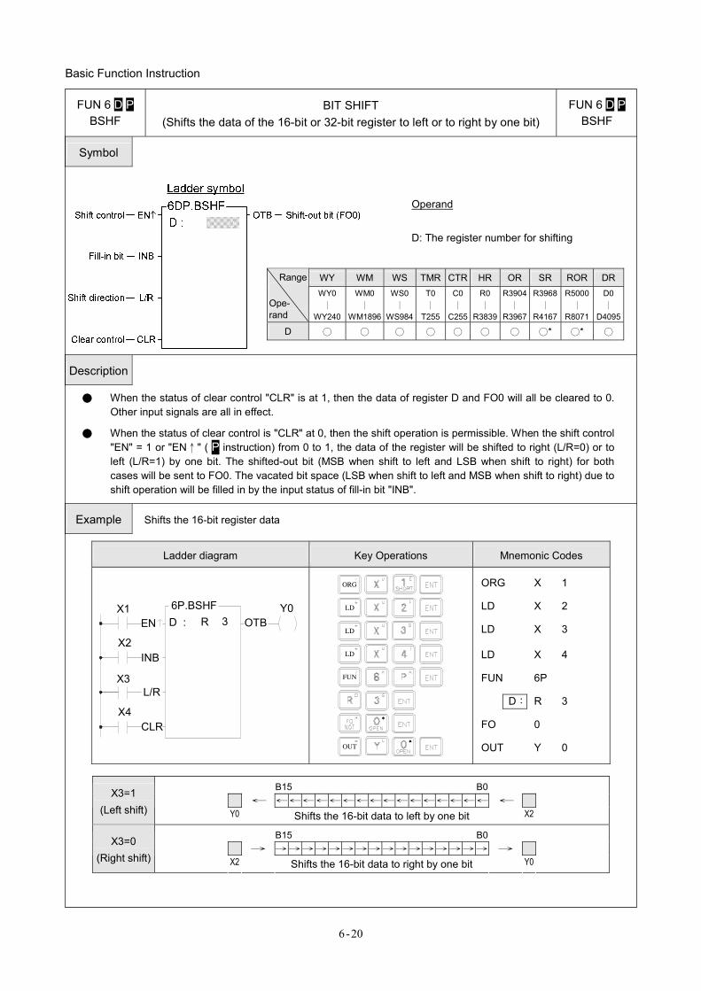
Basic Function Instruction
6-20
FUN 6 D P BSHF
BIT SHIFT (Shifts the data of the 16-bit or 32-bit register to left or to right by one bit)
FUN 6 D P BSHF
Symbol
WY WM WS TMR CTR HR OR SR ROR DRRange
Ope- rand
WY0 ∣
WY240
WM0 ∣
WM1896
WS0∣
WS984
T0 ∣
T255
C0∣
C255
R0 ∣
R3839
R3904 ∣
R3967
R3968 ∣
R4167
R5000∣
R8071
D0 ∣
D4095
D ○ ○ ○ ○ ○ ○ ○ ○* ○* ○
Description
● When the status of clear control "CLR" is at 1, then the data of register D and FO0 will all be cleared to 0. Other input signals are all in effect.
● When the status of clear control is "CLR" at 0, then the shift operation is permissible. When the shift control
"EN" = 1 or "EN↑" ( P instruction) from 0 to 1, the data of the register will be shifted to right (L/R=0) or to left (L/R=1) by one bit. The shifted-out bit (MSB when shift to left and LSB when shift to right) for both cases will be sent to FO0. The vacated bit space (LSB when shift to left and MSB when shift to right) due to shift operation will be filled in by the input status of fill-in bit "INB".
Example Shifts the 16-bit register data
Ladder diagram Key Operations Mnemonic Codes
CLR
OTB
X4
X2
X1
X3
EN
INB
L/R
D : R 3Y06P.BSHF
OUT
FUN
LD
LD
LD
ORG
ORG X 1
LD X 2
LD X 3
LD X 4
FUN 6P
D: R 3
FO 0
OUT Y 0
B15 B0 ← ← ← ← ← ← ← ← ← ← ← ← ← ← ← ← ← ←
X3=1 (Left shift) Y0 Shifts the 16-bit data to left by one bit X2
B15 B0 → → → → → → → → → → → → → → → → → →
X3=0 (Right shift) X2 Shifts the 16-bit data to right by one bit Y0
Operand D: The register number for shifting
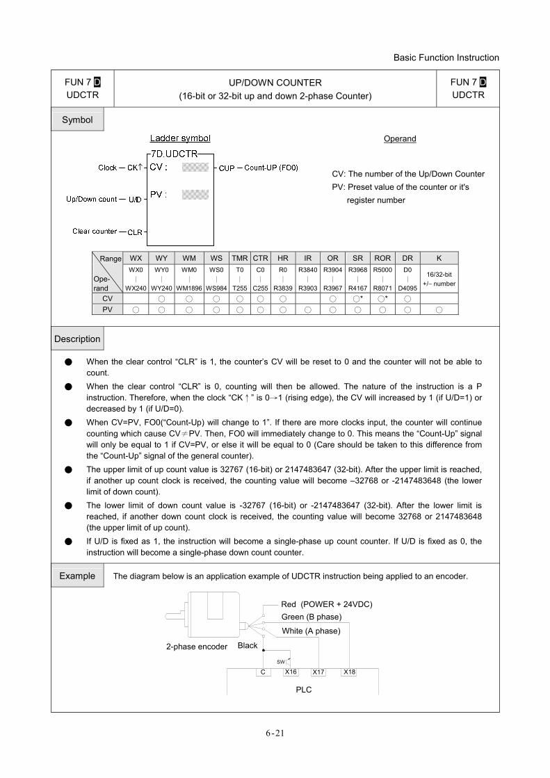
Basic Function Instruction
6 -21
FUN 7 D UDCTR
UP/DOWN COUNTER (16-bit or 32-bit up and down 2-phase Counter)
FUN 7 D UDCTR
Symbol
Operand
CV: The number of the Up/Down Counter PV: Preset value of the counter or it's
register number
WX WY WM WS TMR CTR HR IR OR SR ROR DR K Range
Ope- rand
WX0 ∣
WX240
WY0∣
WY240
WM0 ∣
WM1896
WS0 ∣
WS984
T0∣
T255
C0∣
C255
R0 ∣
R3839
R3840∣
R3903
R3904∣
R3967
R3968∣
R4167
R5000 ∣
R8071
D0 ∣
D4095
16/32-bit +/− number
CV ○ ○ ○ ○ ○ ○ ○ ○* ○* ○ PV ○ ○ ○ ○ ○ ○ ○ ○ ○ ○ ○ ○ ○
Description
● When the clear control “CLR” is 1, the counter’s CV will be reset to 0 and the counter will not be able to count.
● When the clear control “CLR” is 0, counting will then be allowed. The nature of the instruction is a P instruction. Therefore, when the clock “CK↑” is 0→1 (rising edge), the CV will increased by 1 (if U/D=1) or decreased by 1 (if U/D=0).
● When CV=PV, FO0(“Count-Up) will change to 1”. If there are more clocks input, the counter will continue counting which cause CV≠PV. Then, FO0 will immediately change to 0. This means the “Count-Up” signal will only be equal to 1 if CV=PV, or else it will be equal to 0 (Care should be taken to this difference from the “Count-Up” signal of the general counter).
● The upper limit of up count value is 32767 (16-bit) or 2147483647 (32-bit). After the upper limit is reached, if another up count clock is received, the counting value will become –32768 or -2147483648 (the lower limit of down count).
● The lower limit of down count value is -32767 (16-bit) or -2147483647 (32-bit). After the lower limit is reached, if another down count clock is received, the counting value will become 32768 or 2147483648 (the upper limit of up count).
● If U/D is fixed as 1, the instruction will become a single-phase up count counter. If U/D is fixed as 0, the instruction will become a single-phase down count counter.
Example The diagram below is an application example of UDCTR instruction being applied to an encoder.
PLC
2-phase encoder Black
Red (POWER + 24VDC)Green (B phase)
White (A phase)
C X16 X17 X18SW
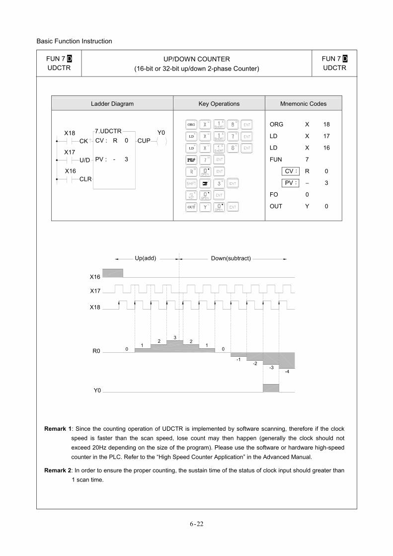
Basic Function Instruction
6-22
FUN 7 D UDCTR
UP/DOWN COUNTER (16-bit or 32-bit up/down 2-phase Counter)
FUN 7 D UDCTR
Ladder Diagram Key Operations Mnemonic Codes
X18
X16
7.UDCTRCV :
PV :
CK
U/D
CLR
R 0 CUP
X17-
Y0
3
ORG
OUT
LD
LD
ORG X 18
LD X 17
LD X 16
FUN 7
CV: R 0
PV: − 3
FO 0
OUT Y 0
X16
X17
X18
R0
Y0
Up(add) Down(subtract)
01
23
21
0
-1-2
-3-4
Remark 1: Since the counting operation of UDCTR is implemented by software scanning, therefore if the clock speed is faster than the scan speed, lose count may then happen (generally the clock should not exceed 20Hz depending on the size of the program). Please use the software or hardware high-speed counter in the PLC. Refer to the “High Speed Counter Application” in the Advanced Manual.
Remark 2: In order to ensure the proper counting, the sustain time of the status of clock input should greater than 1 scan time.
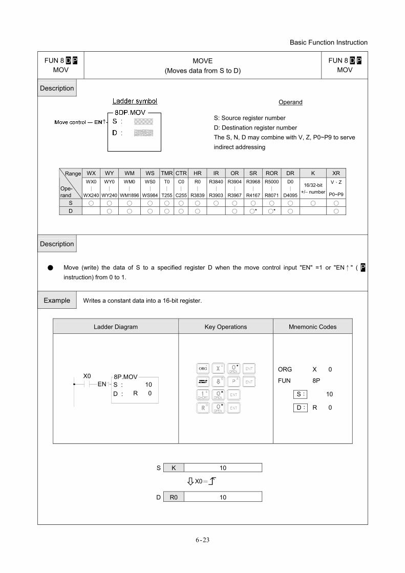
Basic Function Instruction
6 -23
FUN 8 D P MOV
MOVE (Moves data from S to D)
FUN 8 D P MOV
Description
Operand S: Source register number D: Destination register number The S, N, D may combine with V, Z, P0~P9 to serve indirect addressing
WX WY WM WS TMR CTR HR IR OR SR ROR DR K XRRange
Ope- rand
WX0 ∣
WX240
WY0 ∣
WY240
WM0 ∣
WM1896
WS0 ∣
WS984
T0∣
T255
C0∣
C255
R0 ∣
R3839
R3840∣
R3903
R3904∣
R3967
R3968∣
R4167
R5000∣
R8071
D0 ∣
D4095
16/32-bit +/− number
V、Z
P0~P9
S ○ ○ ○ ○ ○ ○ ○ ○ ○ ○ ○ ○ ○ ○ D ○ ○ ○ ○ ○ ○ ○ ○* ○* ○ ○
Description
● Move (write) the data of S to a specified register D when the move control input "EN" =1 or "EN↑" ( P
instruction) from 0 to 1.
Example Writes a constant data into a 16-bit register.
Ladder Diagram Key Operations Mnemonic Codes
X0EN
8P.MOVS :D :
10R 0
ORG
ORG X 0
FUN 8P
S: 10
D: R 0
S K 10
X0=
D R0 10
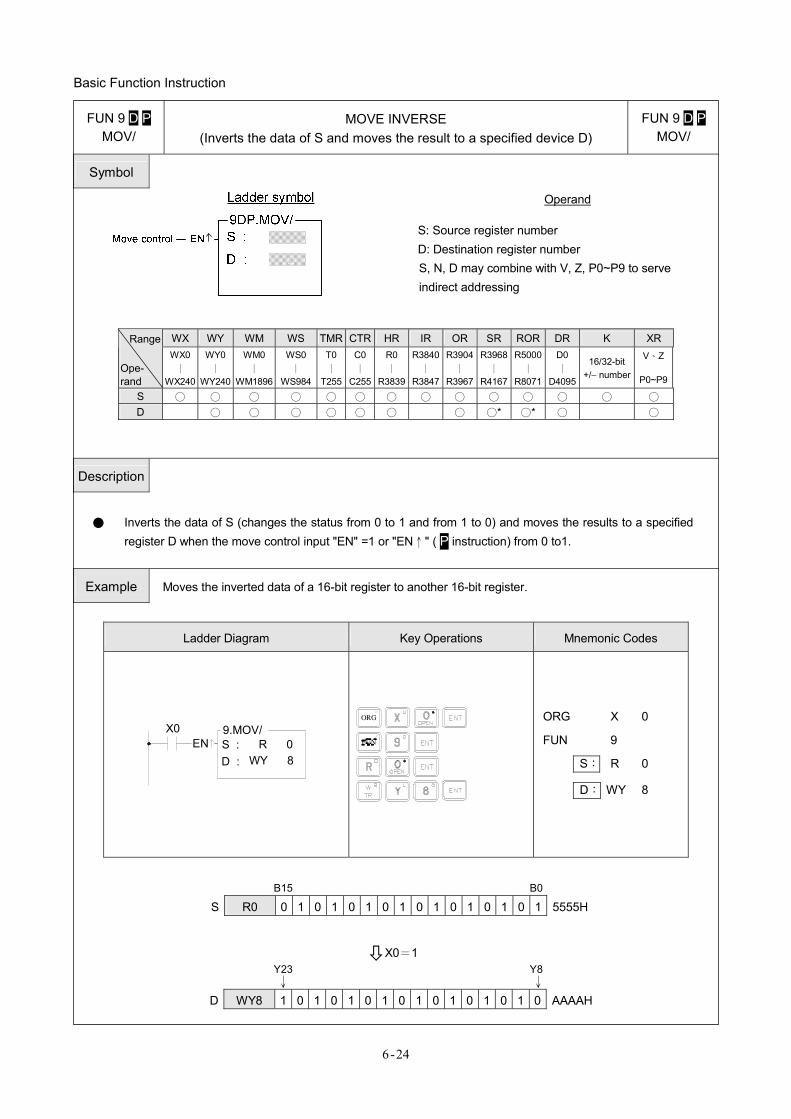
Basic Function Instruction
6-24
FUN 9 D P MOV/
MOVE INVERSE (Inverts the data of S and moves the result to a specified device D)
FUN 9 D P MOV/
Symbol
Operand S: Source register number D: Destination register number S, N, D may combine with V, Z, P0~P9 to serve indirect addressing
WX WY WM WS TMR CTR HR IR OR SR ROR DR K XRRange
Ope- rand
WX0 ∣
WX240
WY0 ∣
WY240
WM0 ∣
WM1896
WS0 ∣
WS984
T0∣
T255
C0∣
C255
R0 ∣
R3839
R3840∣
R3847
R3904∣
R3967
R3968∣
R4167
R5000∣
R8071
D0 ∣
D4095
16/32-bit +/− number
V、Z
P0~P9
S ○ ○ ○ ○ ○ ○ ○ ○ ○ ○ ○ ○ ○ ○ D ○ ○ ○ ○ ○ ○ ○ ○* ○* ○ ○
Description
● Inverts the data of S (changes the status from 0 to 1 and from 1 to 0) and moves the results to a specified
register D when the move control input "EN" =1 or "EN↑" ( P instruction) from 0 to1.
Example Moves the inverted data of a 16-bit register to another 16-bit register.
Ladder Diagram Key Operations Mnemonic Codes
S :X0
END :
9.MOV/R 0
WY 8
ORG
ORG X 0
FUN 9
S: R 0
D: WY 8
B15 B0
S R0 0 1 0 1 0 1 0 1 0 1 0 1 0 1 0 1 5555H
X0=1 Y23 Y8 ↓ ↓
D WY8 1 0 1 0 1 0 1 0 1 0 1 0 1 0 1 0 AAAAH
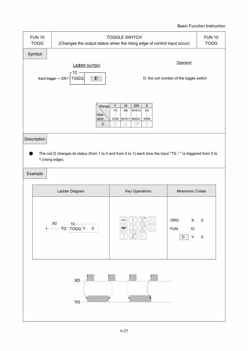
Basic Function Instruction
6-25
FUN 10 TOGG
TOGGLE SWITCH (Changes the output status when the rising edge of control input occur)
FUN 10 TOGG
Symbol
Operand D: the coil number of the toggle switch
Y M SM S Range
Ope- rand
Y0 ∣
Y255
M0∣
M1911
M1912∣
M2001
S0 ∣
S999
D ○ ○ ○* ○
Description
● The coil D changes its status (from 1 to 0 and from 0 to 1) each time the input "TG↑" is triggered from 0 to
1 (rising edge).
Example
Ladder Diagram Key Operations Mnemonic Codes
Y 0TGX0 10.
TOGG
ORG
ORG X 0
FUN 10
D: Y 0
X0
Y0
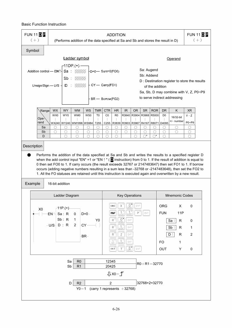
Basic Function Instruction
6-26
FUN 11 D P (+)
ADDITION (Performs addition of the data specified at Sa and Sb and stores the result in D)
FUN 11 D P(+)
Symbol
Operand Sa: Augend Sb: Addend D : Destination register to store the results
of the addition Sa, Sb, D may combine with V, Z, P0~P9 to serve indirect addressing
WX WY WM WS TMR CTR HR IR OR SR ROR DR K XR Range
Ope- rand
WX0 ∣
WX240
WY0∣
WY240
WM0 ∣
WM1896
WS0 ∣
WS984
T0∣
T255
C0∣
C255
R0∣
R3839
R3840∣
R3903
R3904∣
R3967
R3968∣
R4167
R5000∣
R8071
D0 ∣
D4095
16/32-bit +/− number
V、Z P0~P9
Sa ○ ○ ○ ○ ○ ○ ○ ○ ○ ○ ○ ○ ○ ○ Sb ○ ○ ○ ○ ○ ○ ○ ○ ○ ○ ○ ○ ○ ○ D ○ ○ ○ ○ ○ ○ ○ ○* ○* ○ ○
Description
● Performs the addition of the data specified at Sa and Sb and writes the results to a specified register D when the add control input "EN" =1 or "EN↑" ( D instruction) from 0 to 1. If the result of addition is equal to 0 then set FO0 to 1. If carry occurs (the result exceeds 32767 or 2147483647) then set FO1 to 1. If borrow occurs (adding negative numbers resulting in a sum less than -32768 or -2147483648), then set the FO2 to 1. All the FO statuses are retained until this instruction is executed again and overwritten by a new result.
Example 16-bit addition
Ladder Diagram Key Operations Mnemonic Codes
X0EN Sa :
Sb :D :
RRR
012
11P.(+)
Y0U/S
BR
CY
D=0
OUT
ORG
ORG X 0
FUN 11P
Sa: R 0
Sb: R 1
D: R 2
FO 1
OUT Y 0
Sa R0 12345 Sb R1 20425
R0+R1=32770
X0=
D R2 2 32768+2=32770 Y0=1 (carry 1 represents +32768)
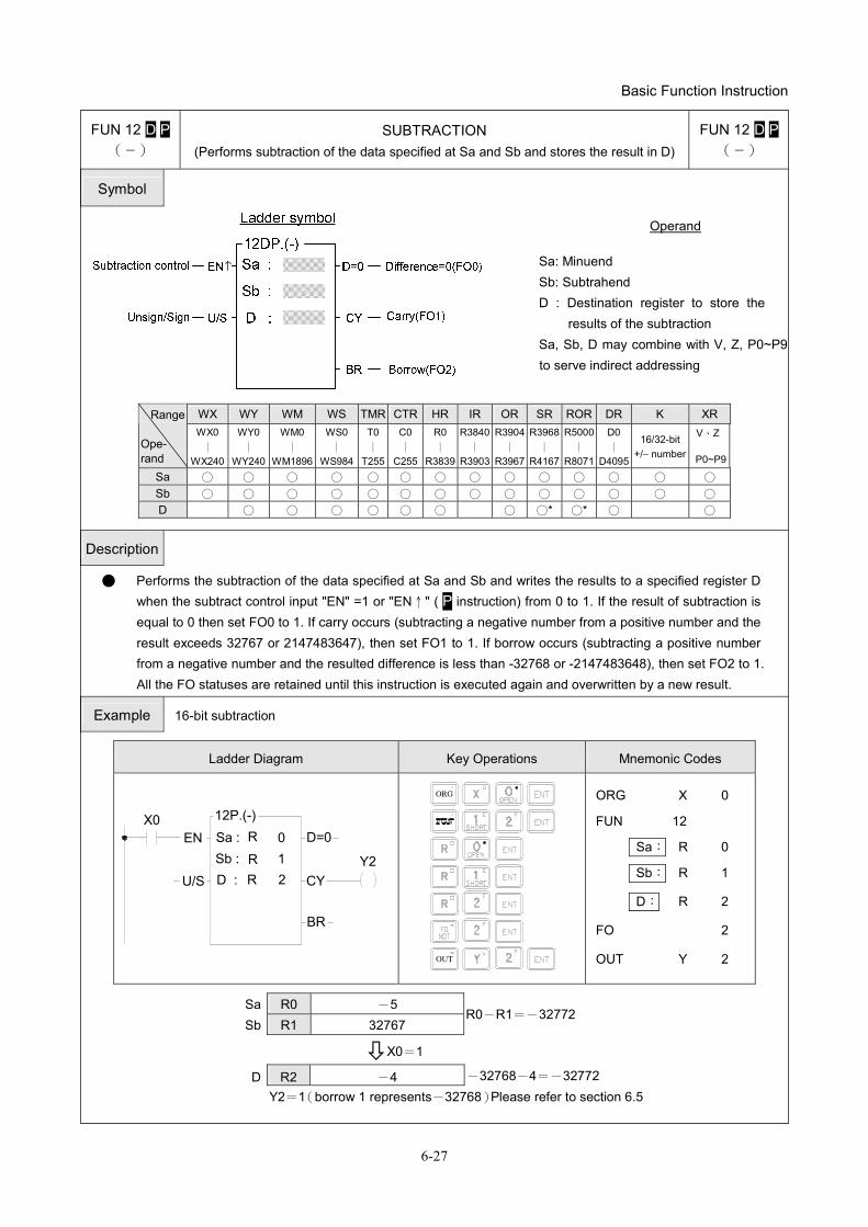
Basic Function Instruction
6-27
FUN 12 D P (−)
SUBTRACTION (Performs subtraction of the data specified at Sa and Sb and stores the result in D)
FUN 12 D P(−)
Symbol
Operand
Sa: Minuend Sb: Subtrahend D : Destination register to store the
results of the subtraction Sa, Sb, D may combine with V, Z, P0~P9to serve indirect addressing
WX WY WM WS TMR CTR HR IR OR SR ROR DR K XRRange
Ope- rand
WX0 ∣
WX240
WY0∣
WY240
WM0 ∣
WM1896
WS0 ∣
WS984
T0∣
T255
C0∣
C255
R0∣
R3839
R3840∣
R3903
R3904∣
R3967
R3968∣
R4167
R5000∣
R8071
D0 ∣
D4095
16/32-bit +/− number
V、Z P0~P9
Sa ○ ○ ○ ○ ○ ○ ○ ○ ○ ○ ○ ○ ○ ○ Sb ○ ○ ○ ○ ○ ○ ○ ○ ○ ○ ○ ○ ○ ○ D ○ ○ ○ ○ ○ ○ ○ ○* ○* ○ ○
Description
● Performs the subtraction of the data specified at Sa and Sb and writes the results to a specified register D when the subtract control input "EN" =1 or "EN↑" ( P instruction) from 0 to 1. If the result of subtraction is equal to 0 then set FO0 to 1. If carry occurs (subtracting a negative number from a positive number and the result exceeds 32767 or 2147483647), then set FO1 to 1. If borrow occurs (subtracting a positive number from a negative number and the resulted difference is less than -32768 or -2147483648), then set FO2 to 1. All the FO statuses are retained until this instruction is executed again and overwritten by a new result.
Example 16-bit subtraction
Ladder Diagram Key Operations Mnemonic Codes
X0EN Sa :
Sb :D :
R
RR
012
12P.(-)D=0
CY
BR
Y2U/S
OUT
ORG
ORG X 0
FUN 12
Sa: R 0
Sb: R 1
D: R 2
FO 2
OUT Y 2
Sa R0 -5 Sb R1 32767
R0-R1=-32772
X0=1
D R2 -4 -32768-4=-32772 Y2=1(borrow 1 represents-32768)Please refer to section 6.5
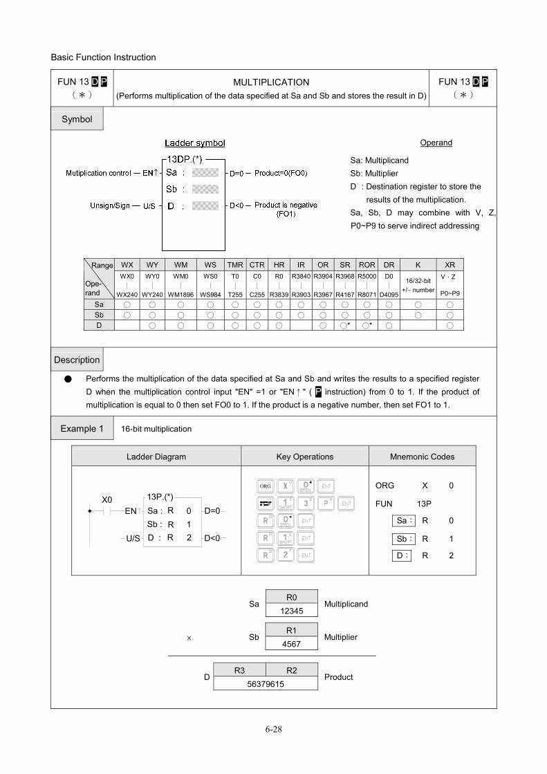
Basic Function Instruction
6-28
FUN 13 D P (*)
MULTIPLICATION (Performs multiplication of the data specified at Sa and Sb and stores the result in D)
FUN 13 D P (*)
Symbol
Operand
Sa: Multiplicand Sb: Multiplier D : Destination register to store the
results of the multiplication. Sa, Sb, D may combine with V, Z, P0~P9 to serve indirect addressing
WX WY WM WS TMR CTR HR IR OR SR ROR DR K XR Range
Ope- rand
WX0 ∣
WX240
WY0 ∣
WY240
WM0 ∣
WM1896
WS0 ∣
WS984
T0 ∣
T255
C0∣
C255
R0∣
R3839
R3840∣
R3903
R3904∣
R3967
R3968∣
R4167
R5000∣
R8071
D0 ∣
D4095
16/32-bit +/− number
V、Z P0~P9
Sa ○ ○ ○ ○ ○ ○ ○ ○ ○ ○ ○ ○ ○ ○ Sb ○ ○ ○ ○ ○ ○ ○ ○ ○ ○ ○ ○ ○ ○ D ○ ○ ○ ○ ○ ○ ○ ○* ○* ○ ○
Description
● Performs the multiplication of the data specified at Sa and Sb and writes the results to a specified register D when the multiplication control input "EN" =1 or "EN↑" ( P instruction) from 0 to 1. If the product of multiplication is equal to 0 then set FO0 to 1. If the product is a negative number, then set FO1 to 1.
Example 1 16-bit multiplication
Ladder Diagram Key Operations Mnemonic Codes
X0EN Sa :
Sb :D :
R
RR
012
13P.(*)D=0
D<0U/S
ORG
ORG X 0
FUN 13P
Sa: R 0
Sb: R 1
D: R 2
R0
Sa12345
Multiplicand
R1
× Sb4567
Multiplier
R3 R2
D 56379615
Product
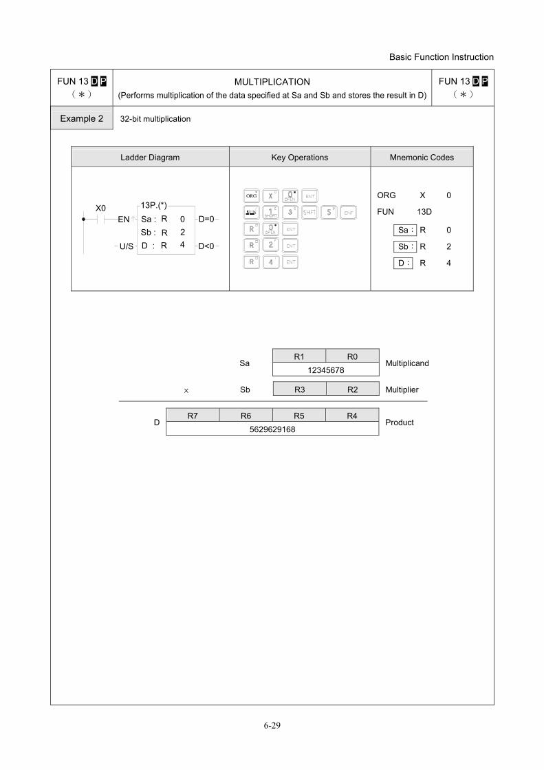
Basic Function Instruction
6-29
FUN 13 D P (*)
MULTIPLICATION (Performs multiplication of the data specified at Sa and Sb and stores the result in D)
FUN 13 D P(*)
Example 2 32-bit multiplication
Ladder Diagram Key Operations Mnemonic Codes
X0EN Sa :
Sb :D :
R
RR
013P.(*)
24 D<0
D=0
U/S
ORG
ORG X 0
FUN 13D
Sa: R 0
Sb: R 2
D: R 4
R1 R0
Sa 12345678
Multiplicand
× Sb R3 R2 Multiplier
R7 R6 R5 R4
D5629629168
Product
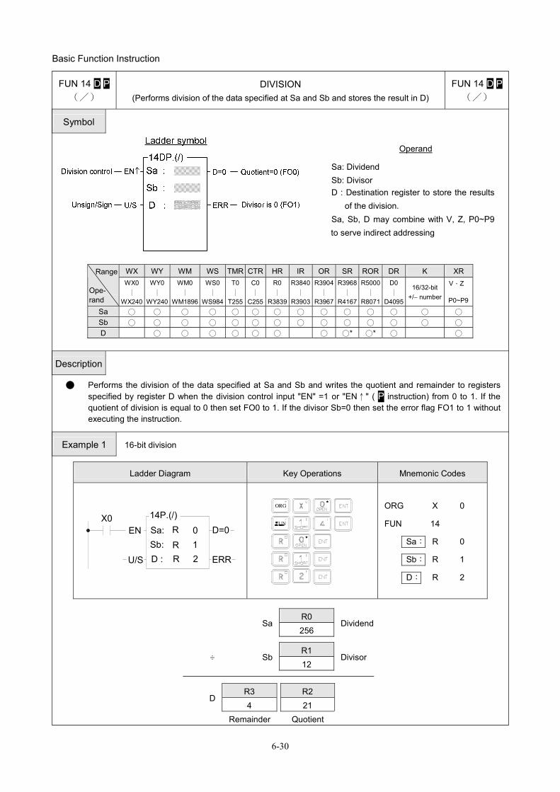
Basic Function Instruction
6-30
FUN 14 D P (/)
DIVISION (Performs division of the data specified at Sa and Sb and stores the result in D)
FUN 14 D P(/)
Symbol
Operand
Sa: Dividend Sb: Divisor D : Destination register to store the results
of the division. Sa, Sb, D may combine with V, Z, P0~P9 to serve indirect addressing
WX WY WM WS TMR CTR HR IR OR SR ROR DR K XR Range
Ope- rand
WX0 ∣
WX240
WY0 ∣
WY240
WM0 ∣
WM1896
WS0 ∣
WS984
T0∣
T255
C0∣
C255
R0 ∣
R3839
R3840∣
R3903
R3904∣
R3967
R3968∣
R4167
R5000∣
R8071
D0 ∣
D4095
16/32-bit +/− number
V、Z P0~P9
Sa ○ ○ ○ ○ ○ ○ ○ ○ ○ ○ ○ ○ ○ ○ Sb ○ ○ ○ ○ ○ ○ ○ ○ ○ ○ ○ ○ ○ ○ D ○ ○ ○ ○ ○ ○ ○ ○* ○* ○ ○
Description
● Performs the division of the data specified at Sa and Sb and writes the quotient and remainder to registers specified by register D when the division control input "EN" =1 or "EN↑" ( P instruction) from 0 to 1. If the quotient of division is equal to 0 then set FO0 to 1. If the divisor Sb=0 then set the error flag FO1 to 1 without executing the instruction.
Example 1 16-bit division
Ladder Diagram Key Operations Mnemonic Codes
X0Sa:Sb:D :
RRR
012
14P.(/)
U/S
EN
ERR
D=0
ORG
ORG X 0
FUN 14
Sa: R 0
Sb: R 1
D: R 2
R0
Sa256
Dividend
R1
÷ Sb12
Divisor
R3 R2
D 4 21
Remainder Quotient
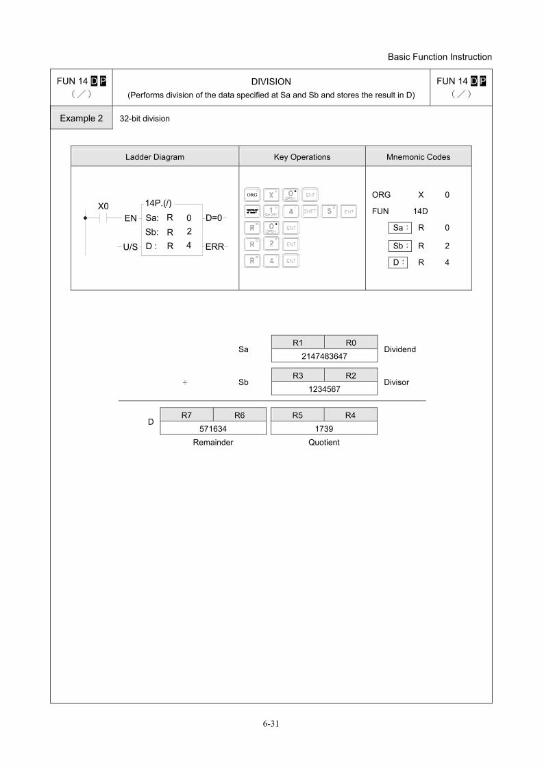
Basic Function Instruction
6-31
FUN 14 D P (/)
DIVISION (Performs division of the data specified at Sa and Sb and stores the result in D)
FUN 14 D P(/)
Example 2 32-bit division
Ladder Diagram Key Operations Mnemonic Codes
X0Sa:Sb:D :
R
RR
02
14P.(/)
4U/S
EN
ERR
D=0
ORG
ORG X 0
FUN 14D
Sa: R 0
Sb: R 2
D: R 4
R1 R0
Sa 2147483647
Dividend
R3 R2
÷ Sb 1234567
Divisor
R7 R6 R5 R4
D 571634 1739
Remainder Quotient
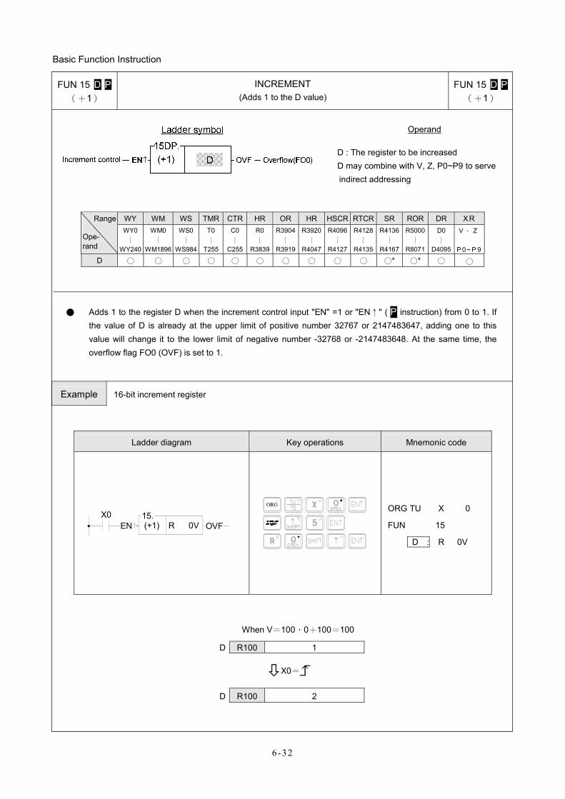
Basic Function Instruction
6-32
FUN 15 D P (+1)
INCREMENT (Adds 1 to the D value)
FUN 15 D P(+1)
Operand
D : The register to be increased D may combine with V, Z, P0~P9 to serve indirect addressing
WY WM WS TMR CTR HR OR HR HSCR RTCR SR ROR DR XR Range
Ope- rand
WY0 ∣
WY240
WM0∣
WM1896
WS0 ∣
WS984
T0 ∣
T255
C0 ∣
C255
R0 ∣
R3839
R3904∣
R3919
R3920∣
R4047
R4096∣
R4127
R4128∣
R4135
R4136∣
R4167
R5000 ∣
R8071
D0 ∣
D4095
V 、 Z
P 0 ~ P 9
D ○ ○ ○ ○ ○ ○ ○ ○ ○ ○ ○* ○* ○ ○
● Adds 1 to the register D when the increment control input "EN" =1 or "EN↑" ( P instruction) from 0 to 1. If the value of D is already at the upper limit of positive number 32767 or 2147483647, adding one to this value will change it to the lower limit of negative number -32768 or -2147483648. At the same time, the overflow flag FO0 (OVF) is set to 1.
Example 16-bit increment register
Ladder diagram Key operations Mnemonic code
15.(+1) R 0V
X0EN OVF
ORG
ORG TU X 0
FUN 15
D : R 0V
When V=100,0+100=100
D R100 1
X0=
D R100 2
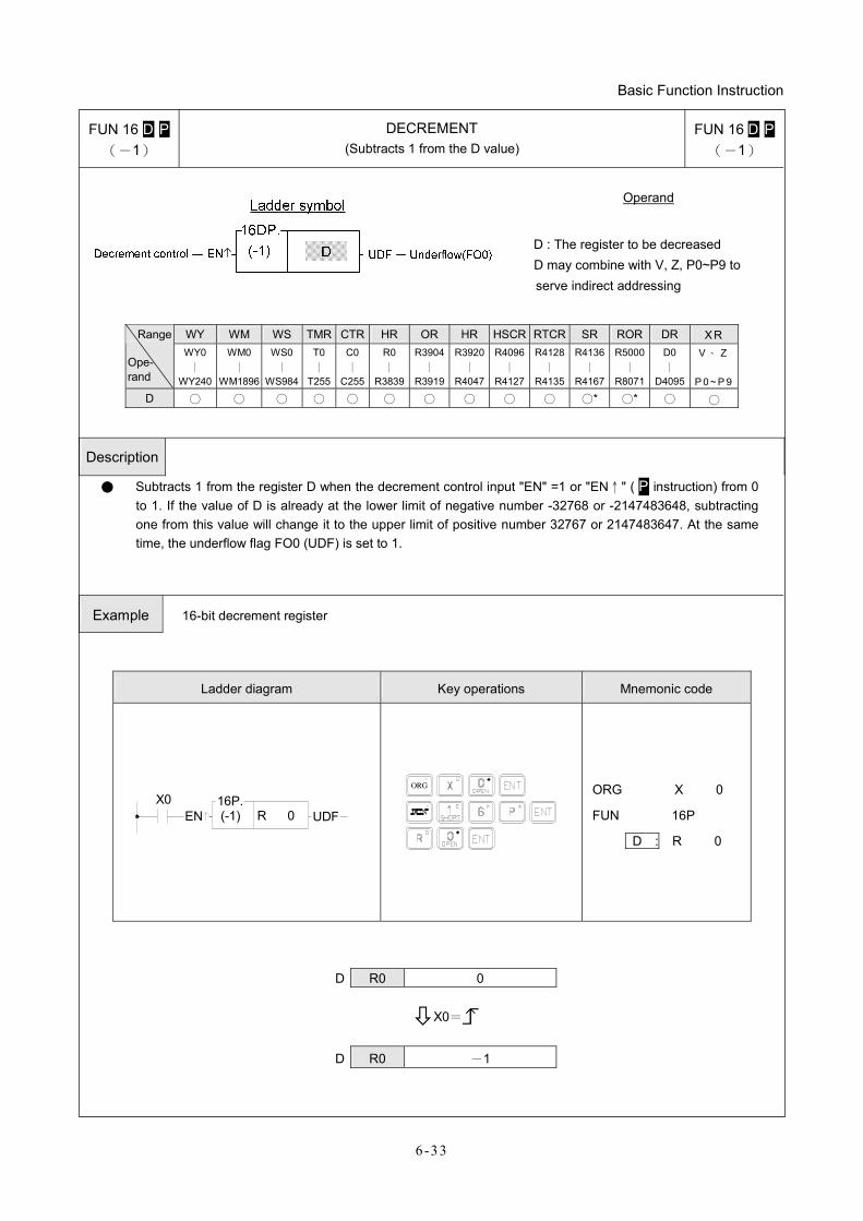
Basic Function Instruction
6-33
FUN 16 D P (-1)
DECREMENT (Subtracts 1 from the D value)
FUN 16 D P(-1)
Operand
D : The register to be decreased D may combine with V, Z, P0~P9 to serve indirect addressing
WY WM WS TMR CTR HR OR HR HSCR RTCR SR ROR DR XR Range
Ope- rand
WY0 ∣
WY240
WM0 ∣
WM1896
WS0 ∣
WS984
T0 ∣
T255
C0∣
C255
R0 ∣
R3839
R3904∣
R3919
R3920∣
R4047
R4096∣
R4127
R4128∣
R4135
R4136∣
R4167
R5000 ∣
R8071
D0 ∣
D4095
V 、 Z
P 0 ~ P 9
D ○ ○ ○ ○ ○ ○ ○ ○ ○ ○ ○* ○* ○ ○
Description
● Subtracts 1 from the register D when the decrement control input "EN" =1 or "EN↑" ( P instruction) from 0 to 1. If the value of D is already at the lower limit of negative number -32768 or -2147483648, subtracting one from this value will change it to the upper limit of positive number 32767 or 2147483647. At the same time, the underflow flag FO0 (UDF) is set to 1.
Example 16-bit decrement register
Ladder diagram Key operations Mnemonic code
16P.(-1) R 0
X0EN UDF
ORG
ORG X 0
FUN 16P
D : R 0
D R0 0
X0=
D R0 -1
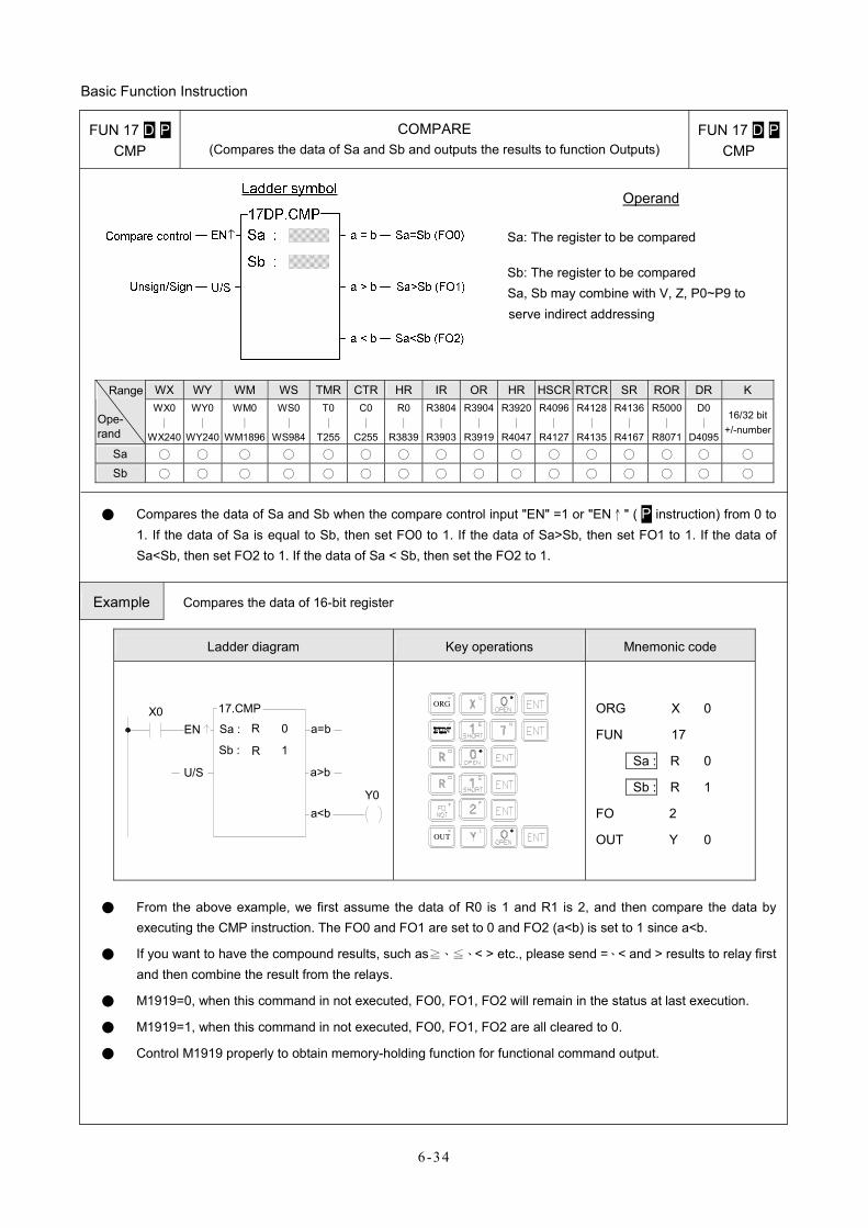
Basic Function Instruction
6-34
FUN 17 D P CMP
COMPARE (Compares the data of Sa and Sb and outputs the results to function Outputs)
FUN 17 D PCMP
Operand
Sa: The register to be compared
Sb: The register to be compared Sa, Sb may combine with V, Z, P0~P9 to serve indirect addressing
WX WY WM WS TMR CTR HR IR OR HR HSCR RTCR SR ROR DR K Range
Ope- rand
WX0 ∣
WX240
WY0 ∣
WY240
WM0∣
WM1896
WS0 ∣
WS984
T0 ∣
T255
C0 ∣
C255
R0 ∣
R3839
R3804∣
R3903
R3904∣
R3919
R3920∣
R4047
R4096∣
R4127
R4128∣
R4135
R4136 ∣
R4167
R5000 ∣
R8071
D0 ∣
D4095
16/32 bit+/-number
Sa ○ ○ ○ ○ ○ ○ ○ ○ ○ ○ ○ ○ ○ ○ ○ ○ Sb ○ ○ ○ ○ ○ ○ ○ ○ ○ ○ ○ ○ ○ ○ ○ ○
● Compares the data of Sa and Sb when the compare control input "EN" =1 or "EN↑" ( P instruction) from 0 to 1. If the data of Sa is equal to Sb, then set FO0 to 1. If the data of Sa>Sb, then set FO1 to 1. If the data of Sa<Sb, then set FO2 to 1. If the data of Sa < Sb, then set the FO2 to 1.
Example Compares the data of 16-bit register
Ladder diagram Key operations Mnemonic code
X0EN Sa :
Sb :
R
R
0
1
17.CMP
a=b
a>b
a<bY0
U/S
OUT
ORG
ORG X 0
FUN 17
Sa : R 0
Sb : R 1
FO 2
OUT Y 0
● From the above example, we first assume the data of R0 is 1 and R1 is 2, and then compare the data by
executing the CMP instruction. The FO0 and FO1 are set to 0 and FO2 (a<b) is set to 1 since a<b.
● If you want to have the compound results, such as≧、≦、< > etc., please send =、< and > results to relay first and then combine the result from the relays.
● M1919=0, when this command in not executed, FO0, FO1, FO2 will remain in the status at last execution.
● M1919=1, when this command in not executed, FO0, FO1, FO2 are all cleared to 0.
● Control M1919 properly to obtain memory-holding function for functional command output.
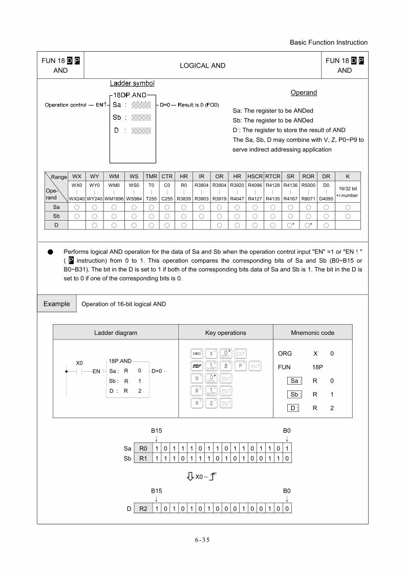
Basic Function Instruction
6-35
FUN 18 D P AND
LOGICAL AND FUN 18 D P
AND
Operand
Sa: The register to be ANDed Sb: The register to be ANDed D : The register to store the result of AND The Sa, Sb, D may combine with V, Z, P0~P9 to serve indirect addressing application
WX WY WM WS TMR CTR HR IR OR HR HSCR RTCR SR ROR DR K Range
Ope- rand
WX0 ∣
WX240
WY0 ∣
WY240
WM0∣
WM1896
WS0 ∣
WS984
T0 ∣
T255
C0∣
C255
R0 ∣
R3839
R3804∣
R3903
R3904∣
R3919
R3920∣
R4047
R4096∣
R4127
R4128∣
R4135
R4136 ∣
R4167
R5000 ∣
R8071
D0 ∣
D4095
16/32 bit+/-number
Sa ○ ○ ○ ○ ○ ○ ○ ○ ○ ○ ○ ○ ○ ○ ○ ○ Sb ○ ○ ○ ○ ○ ○ ○ ○ ○ ○ ○ ○ ○ ○ ○ ○ D ○ ○ ○ ○ ○ ○ ○ ○ ○ ○ ○* ○* ○
● Performs logical AND operation for the data of Sa and Sb when the operation control input "EN" =1 or "EN↑" ( P instruction) from 0 to 1. This operation compares the corresponding bits of Sa and Sb (B0~B15 or B0~B31). The bit in the D is set to 1 if both of the corresponding bits data of Sa and Sb is 1. The bit in the D is set to 0 if one of the corresponding bits is 0.
Example Operation of 16-bit logical AND
Ladder diagram Key operations Mnemonic code
X0EN Sa :
Sb :
D :
R
R
R
0
1
2
18P.AND
D=0
ORG
ORG X 0
FUN 18P
Sa : R 0
Sb : R 1
D : R 2
B15 B0 ↓ ↓
Sa R0 1 0 1 1 1 0 1 1 0 1 1 0 1 1 0 1 Sb R1 1 1 1 0 1 1 1 0 1 0 1 0 0 1 1 0
X0=
B15 B0 ↓ ↓
D R2 1 0 1 0 1 0 1 0 0 0 1 0 0 1 0 0
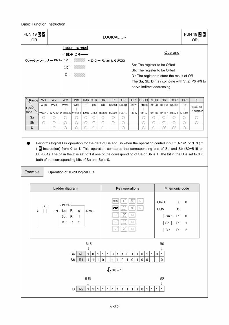
Basic Function Instruction
6-36
FUN 19 D P OR
LOGICAL OR FUN 19 D P
OR
Operand
Sa: The register to be ORed Sb: The register to be ORed D : The register to store the result of OR The Sa, Sb, D may combine with V, Z, P0~P9 to serve indirect addressing
WX WY WM WS TMR CTR HR IR OR HR HSCR RTCR SR ROR DR K Range
Ope- rand
WX0 ∣
WX240
WY0 ∣
WY240
WM0∣
WM1896
WS0 ∣
WS984
T0 ∣
T255
C0∣
C255
R0 ∣
R3839
R3804∣
R3903
R3904∣
R3919
R3920∣
R4047
R4096∣
R4127
R4128∣
R4135
R4136 ∣
R4167
R5000 ∣
R8071
D0 ∣
D4095
16/32 bit+/-number
Sa ○ ○ ○ ○ ○ ○ ○ ○ ○ ○ ○ ○ ○ ○ ○ Sb ○ ○ ○ ○ ○ ○ ○ ○ ○ ○ ○ ○ ○ ○ ○ D ○ ○ ○ ○ ○ ○ ○ ○ ○ ○* ○* ○
● Performs logical OR operation for the data of Sa and Sb when the operation control input "EN" =1 or "EN↑" ( P instruction) from 0 to 1. This operation compares the corresponding bits of Sa and Sb (B0~B15 or B0~B31). The bit in the D is set to 1 if one of the corresponding of Sa or Sb is 1. The bit in the D is set to 0 if both of the corresponding bits of Sa and Sb is 0.
Example Operation of 16-bit logical OR
Ladder diagram Key operations Mnemonic code
X0EN Sa :
Sb :
D :
R
R
R
0
1
2
19.OR
D=0
ORG
ORG X 0
FUN 19
Sa : R 0
Sb : R 1
D : R 2
B15 B0 ↓ ↓
Sa R0 1 0 1 1 1 0 1 1 0 1 1 0 1 1 0 1 Sb R1 1 1 1 0 1 1 1 0 1 0 1 0 0 1 1 0
X0=1
B15 B0 ↓ ↓
D R2 1 1 1 1 1 1 1 1 1 1 1 0 1 1 1 1
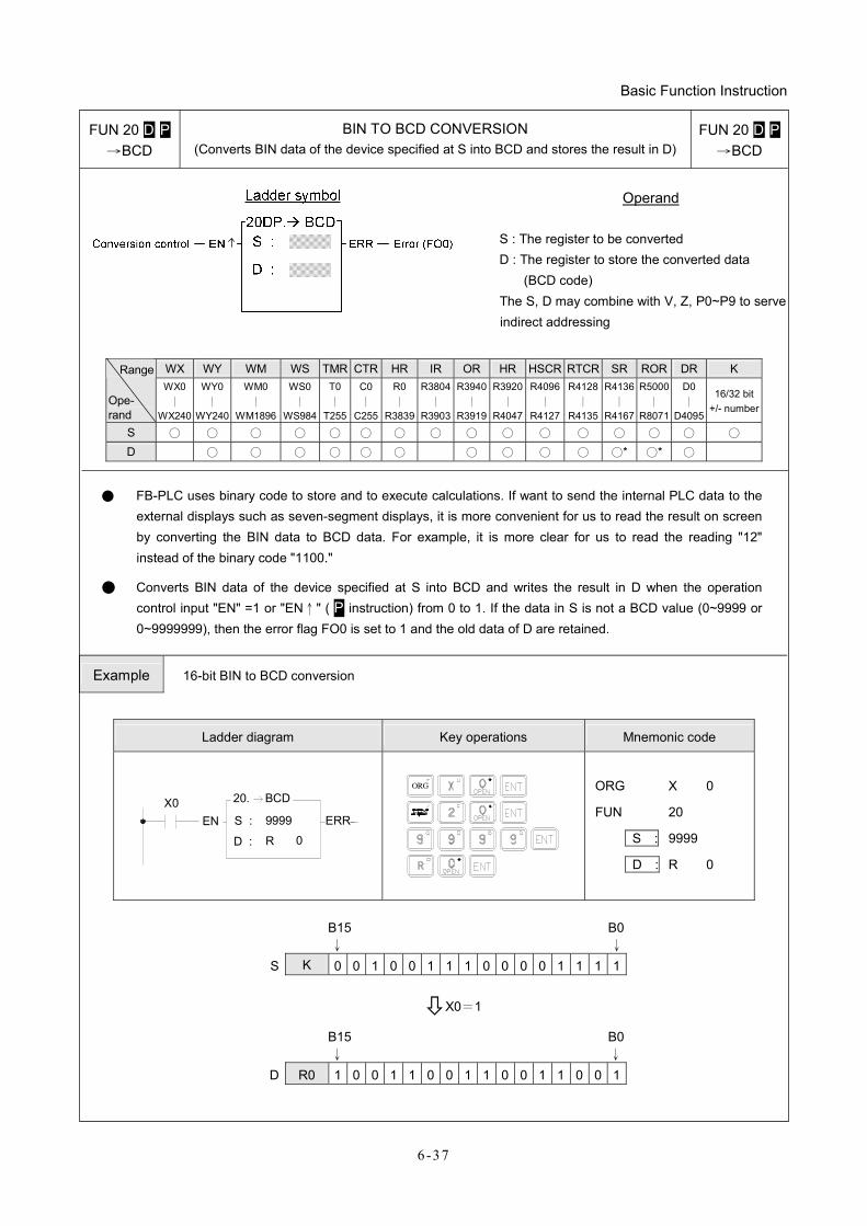
Basic Function Instruction
6-37
FUN 20 D P →BCD
BIN TO BCD CONVERSION (Converts BIN data of the device specified at S into BCD and stores the result in D)
FUN 20 D P→BCD
Operand
S : The register to be converted D : The register to store the converted data
(BCD code) The S, D may combine with V, Z, P0~P9 to serve indirect addressing
WX WY WM WS TMR CTR HR IR OR HR HSCR RTCR SR ROR DR K Range
Ope- rand
WX0 ∣
WX240
WY0 ∣
WY240
WM0 ∣
WM1896
WS0 ∣
WS984
T0 ∣
T255
C0∣
C255
R0∣
R3839
R3804∣
R3903
R3940∣
R3919
R3920∣
R4047
R4096∣
R4127
R4128∣
R4135
R4136 ∣
R4167
R5000 ∣
R8071
D0 ∣
D4095
16/32 bit+/- number
S ○ ○ ○ ○ ○ ○ ○ ○ ○ ○ ○ ○ ○ ○ ○ ○ D ○ ○ ○ ○ ○ ○ ○ ○ ○ ○ ○* ○* ○
● FB-PLC uses binary code to store and to execute calculations. If want to send the internal PLC data to the external displays such as seven-segment displays, it is more convenient for us to read the result on screen by converting the BIN data to BCD data. For example, it is more clear for us to read the reading "12" instead of the binary code "1100."
● Converts BIN data of the device specified at S into BCD and writes the result in D when the operation control input "EN" =1 or "EN↑" ( P instruction) from 0 to 1. If the data in S is not a BCD value (0~9999 or 0~9999999), then the error flag FO0 is set to 1 and the old data of D are retained.
Example 16-bit BIN to BCD conversion
Ladder diagram Key operations Mnemonic code
X0EN S :
D : R
9999
0
20. BCD
ERR
ORG
ORG X 0
FUN 20
S : 9999
D : R 0
B15 B0 ↓ ↓
S K 0 0 1 0 0 1 1 1 0 0 0 0 1 1 1 1
X0=1
B15 B0 ↓ ↓
D R0 1 0 0 1 1 0 0 1 1 0 0 1 1 0 0 1
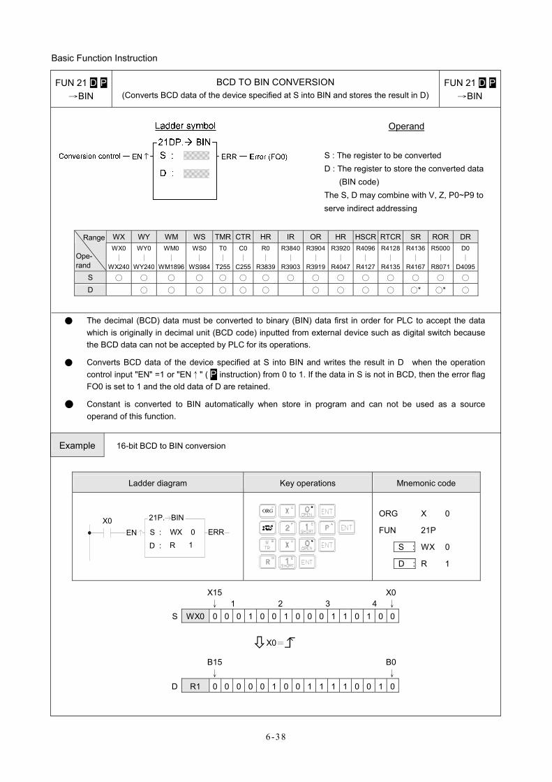
Basic Function Instruction
6-38
FUN 21 D P →BIN
BCD TO BIN CONVERSION (Converts BCD data of the device specified at S into BIN and stores the result in D)
FUN 21 D P→BIN
Operand
S : The register to be converted D : The register to store the converted data
(BIN code) The S, D may combine with V, Z, P0~P9 to serve indirect addressing
WX WY WM WS TMR CTR HR IR OR HR HSCR RTCR SR ROR DR Range
Ope- rand
WX0 ∣
WX240
WY0 ∣
WY240
WM0 ∣
WM1896
WS0 ∣
WS984
T0 ∣
T255
C0∣
C255
R0 ∣
R3839
R3840∣
R3903
R3904∣
R3919
R3920∣
R4047
R4096∣
R4127
R4128 ∣
R4135
R4136 ∣
R4167
R5000 ∣
R8071
D0 ∣
D4095
S ○ ○ ○ ○ ○ ○ ○ ○ ○ ○ ○ ○ ○ ○ ○ D ○ ○ ○ ○ ○ ○ ○ ○ ○ ○ ○* ○* ○
● The decimal (BCD) data must be converted to binary (BIN) data first in order for PLC to accept the data which is originally in decimal unit (BCD code) inputted from external device such as digital switch because the BCD data can not be accepted by PLC for its operations.
● Converts BCD data of the device specified at S into BIN and writes the result in D when the operation control input "EN" =1 or "EN↑" ( P instruction) from 0 to 1. If the data in S is not in BCD, then the error flag FO0 is set to 1 and the old data of D are retained.
● Constant is converted to BIN automatically when store in program and can not be used as a source operand of this function.
Example 16-bit BCD to BIN conversion
Ladder diagram Key operations Mnemonic code
X0EN S :
D : R
WX 01
21P. BIN
ERR
ORG
ORG X 0
FUN 21P
S : WX 0
D : R 1
X15 X0 ↓ 1 2 3 4 ↓
S WX0 0 0 0 1 0 0 1 0 0 0 1 1 0 1 0 0
X0=
B15 B0 ↓ ↓
D R1 0 0 0 0 0 1 0 0 1 1 1 1 0 0 1 0
Chapter 7 Advanced Function Instructions
Flow control instructions1 (FUN22) ............................................................... 7 -1
Arithmetical operation instructions (FUN23~32)............................................7-2 ~ 7 -9
Logical operation instructions (FUN35~36)............................................7-10 ~ 7-13
Comparison instructions (FUN37) ...............................................................7-14
Data movement instructions1 (FUN40~50)............................................ 7-15 ~ 7-25
Shifting/Rotating instructions1 (FUN51~54)............................................ 7-26 ~ 7-29
Code conversion instructions (FUN55~64)............................................ 7-30 ~ 7-46
Flow control instructions2 (FUN65~71)............................................ 7-47 ~ 7-54
I/O instructions (FUN74~86)............................................ 7-55 ~ 7-72
Cumulative timer instructions (FUN87~89)............................................ 7-73 ~ 7-74
Watchdog timer instructions (FUN90~91).............................................7-75 ~ 7-76
High speed counting/timing (FUN92~93).............................................7-77 ~ 7-78
Report printing instructions (FUN94) ....................................................7-79 ~ 7-80
Slow up/Slow down instructions (FUN95) ....................................................7-81 ~ 7-82
Table instructions (FUN100~114)....................................... 7-84 ~ 7-101
Matrix instructions (FUN120~130)..................................7-103 ~ 7-113
NC positioning instructions (FUN140~143).............................7-114 ~ 7-119
Enable/Disable instructions (FUN145~146).............................7-120 ~ 7-121
Communication instructions (FUN150~151).............................7-122 ~ 7-123
Date movement instructions2 (FUN160) ........................................... 7-124 ~ 7-125
Floating Point Number operation instructions(FUN200~213)..........7-126 ~ 7-140
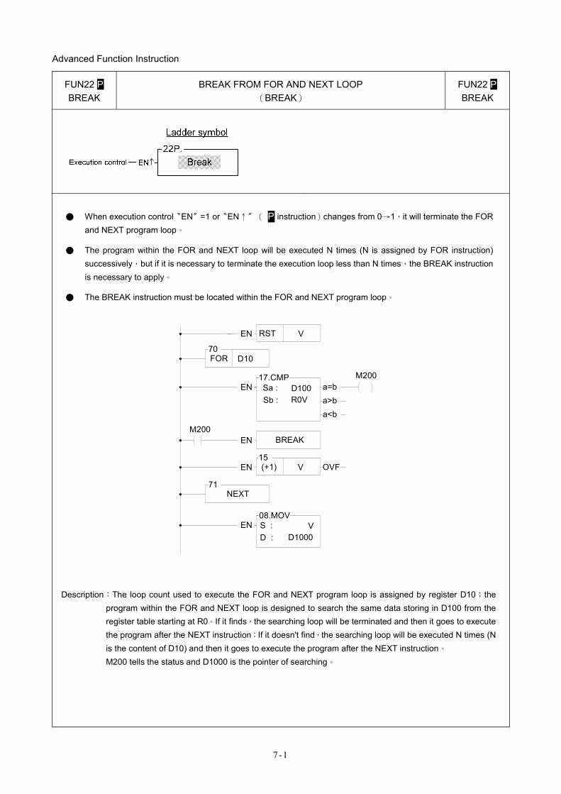
Advanced Function Instruction
7-1
FUN22 P BREAK
BREAK FROM FOR AND NEXT LOOP (BREAK)
FUN22 P BREAK
● When execution control〝EN〞=1 or〝EN↑〞( P instruction)changes from 0→1,it will terminate the FOR and NEXT program loop。
● The program within the FOR and NEXT loop will be executed N times (N is assigned by FOR instruction) successively,but if it is necessary to terminate the execution loop less than N times,the BREAK instruction is necessary to apply。
● The BREAK instruction must be located within the FOR and NEXT program loop。
Sa :Sb :
a=bM200
RST V
M200
R0V
FOR D10
EN
70
EN17.CMP
BREAKEN
(+1) VEN
NEXT71
EN08.MOV
15
D100a>ba<b
OVF
S :D : D1000
V
Description:The loop count used to execute the FOR and NEXT program loop is assigned by register D10;the
program within the FOR and NEXT loop is designed to search the same data storing in D100 from the register table starting at R0。If it finds,the searching loop will be terminated and then it goes to execute the program after the NEXT instruction;If it doesn't find,the searching loop will be executed N times (N is the content of D10) and then it goes to execute the program after the NEXT instruction。 M200 tells the status and D1000 is the pointer of searching。
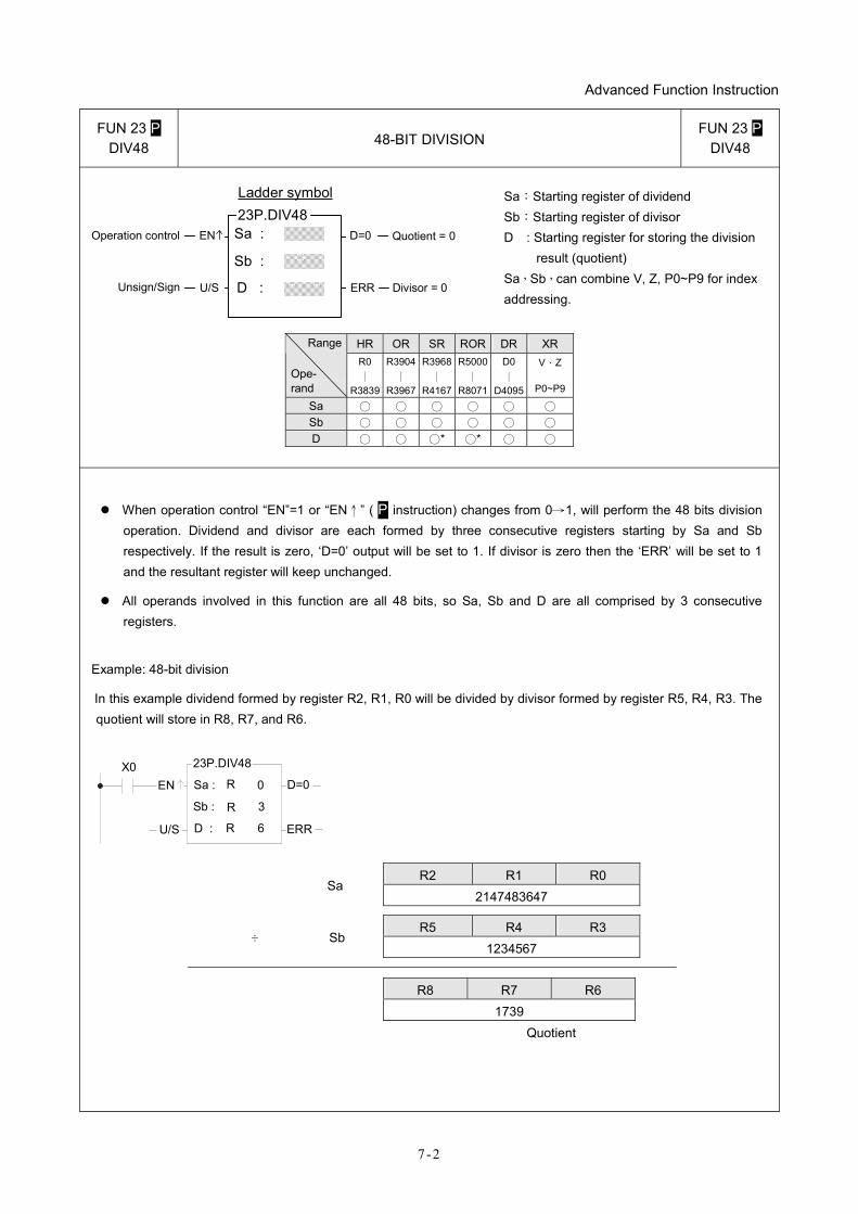
Advanced Function Instruction
7-2
FUN 23 P DIV48 48-BIT DIVISION
FUN 23 P DIV48
Sa :
D :
ENOperation control
Ladder symbol 23P.DIV48
Sb :
ERR
D=0 Quotient = 0
Divisor = 0U/SUnsign/Sign
Sa:Starting register of dividend Sb:Starting register of divisor D : Starting register for storing the division
result (quotient) Sa,Sb,can combine V, Z, P0~P9 for index addressing.
HR OR SR ROR DR XR Range
Ope- rand
R0 ∣
R3839
R3904∣
R3967
R3968∣
R4167
R5000∣
R8071
D0 ∣
D4095
V、Z
P0~P9
Sa ○ ○ ○ ○ ○ ○ Sb ○ ○ ○ ○ ○ ○ D ○ ○ ○* ○* ○ ○
When operation control “EN”=1 or “EN↑” ( P instruction) changes from 0→1, will perform the 48 bits division operation. Dividend and divisor are each formed by three consecutive registers starting by Sa and Sb respectively. If the result is zero, ‘D=0’ output will be set to 1. If divisor is zero then the ‘ERR’ will be set to 1 and the resultant register will keep unchanged.
All operands involved in this function are all 48 bits, so Sa, Sb and D are all comprised by 3 consecutive registers.
Example: 48-bit division
In this example dividend formed by register R2, R1, R0 will be divided by divisor formed by register R5, R4, R3. The quotient will store in R8, R7, and R6.
X0EN Sa :
Sb :
D :
R
R
R
0
3
6
23P.DIV48
D=0
ERRU/S
R2 R1 R0 Sa
2147483647
R5 R4 R3 ÷ Sb
1234567
R8 R7 R6
1739
Quotient
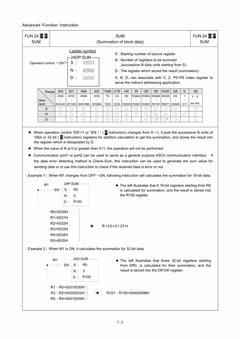
Advanced Function Instruction
7-3
FUN 24 D P SUM
SUM (Summation of block data)
FUN 24 D PSUM
S :
D :
ENOperation control
Ladder symbol 24DP.SUM
N :
S : Starting number of source register
N : Number of registers to be summed (successive N data units starting from S)
D : The register which stored the result (summation)
S, N, D, can associate with V, Z, P0~P9 index register to serve the indirect addressing application.
WX WY WM WS TMR CTR HR IR OR SR ROR DR K XR Range
Ope- rand
WX0 ∣
WX240
WY0 ∣
WY240
WM0 ∣
WM1896
WS0 ∣
WS984
T0∣
T255
C0∣
C255
R0∣
R3839
R3840∣
R3903
R3904∣
R3967
R3968∣
R4167
R5000 ∣
R8071
D0 ∣
D4095
1 ∣
511
V、Z P0~P9
S ○ ○ ○ ○ ○ ○ ○ ○ ○ ○ ○ ○ ○ N ○ ○ ○ ○ ○ ○ ○ ○ ○ ○ ○ ○ ○ ○ D ○ ○ ○ ○ ○ ○ ○ ○* ○* ○ ○
When operation control “EN”=1 or “EN↑” ( P instruction) changes from 0→1, it puts the successive N units of 16bit or 32 bit ( D instruction) registers for addition calculation to get the summation, and stores the result into the register which is designated by D.
When the value of N is 0 or greater than 511, the operation will not be performed.
Communication port1 or port2 can be used to serve as a general purpose ASCII communication interface. If the data error detecting method is Check-Sum, this instruction can be used to generate the sum value for sending data or ot use this instruction to check if the received data is error or not.
〈Example 1〉When M1 changes from OFF→ON, following instruction will calculates the summation for 16-bit data.
M1EN S :
N :
D :
R0
6
R100
24P.SUM
The left illustrates that 6 16-bit registers starting from R0 is calculated for summation, and the result is stored into the R100 register.
R0=0030H R1=0031H R2=0032H R3=0033H R4=0034H R5=0035H
〈Example 2〉When M1 is ON, it calculates the summation for 32-bit data.
S :
N :
D :
R0
3
R100
24D.SUM
ENM1
The left illustrates that three 32-bit registers starting from DR0, is calculated for their summation, and the result is stored into the DR100 register.
R1,R0=00310030H R3,R2=00330032H R101,R100=00A5009BH R5,R4=00410039H
R100=012FH
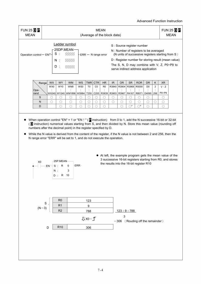
Advanced Function Instruction
7-4
FUN 25 D P MEAN
MEAN (Average of the block data)
FUN 25 D PMEAN
S :
D :
ENOperation control
Ladder symbol 25DP.MEAN
N :
ERR N range error
S : Source register number
N : Number of registers to be averaged (N units of successive registers starting from S)
D : Register number for storing result (mean value)
The S, N, D may combine with V, Z, P0~P9 to serve indirect address application
WX WY WM WS TMR CTR HR IR OR SR ROR DR K XR Range
Ope- rand
WX0 ∣
WX240
WY0 ∣
WY240
WM0 ∣
WM1896
WS0∣
WS984
T0∣
T255
C0∣
C255
R0 ∣
R3839
R3840∣
R3903
R3904∣
R3967
R3968∣
R4167
R5000 ∣
R8071
D0 ∣
D4095
2 ∣
256
V、Z P0~P9
S ○ ○ ○ ○ ○ ○ ○ ○ ○ ○ ○ ○ ○ N ○ ○ ○ ○ ○ ○ ○ ○ ○ ○ ○ ○ ○ ○ D ○ ○ ○ ○ ○ ○ ○ ○* ○* ○ ○
When operation control "EN" = 1 or "EN↑" ( P instruction) from 0 to 1, add the N successive 16-bit or 32-bit ( D instruction) numerical values starting from S, and then divided by N. Store this mean value (rounding off numbers after the decimal point) in the register specified by D.
While the N value is derived from the content of the register, if the N value is not between 2 and 256, then the N range error "ERR" will be set to 1, and do not execute the operation.
S :
N :
D :
3
25P.MEANX0EN ERRR 0
R 10
At left, the example program gets the mean value of the 3 successive 16-bit registers starting from R0, and stores the results into the 16-bit register R10
R0 123 R1 9
S (N=3)
R2 788 123+9+788
X0=
3 =306 (Rouding off the remainder)
D R10 306
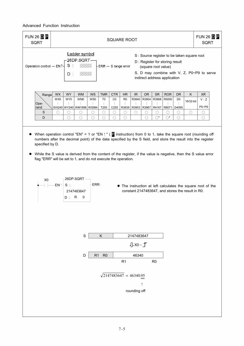
Advanced Function Instruction
7-5
FUN 26 D P SQRT
SQUARE ROOT FUN 26 D P
SQRT
S : Source register to be taken square root
D : Register for storing result (square root value)
S, D may combine with V, Z, P0~P9 to serve indirect address application
WX WY WM WS TMR CTR HR IR OR SR ROR DR K XRRange
Ope- rand
WX0 ∣
WX240
WY0∣
WY240
WM0 ∣
WM1896
WS0 ∣
WS984
T0 ∣
T255
C0 ∣
C255
R0 ∣
R3839
R3840∣
R3903
R3904∣
R3967
R3968∣
R4167
R5000∣
R8071
D0 ∣
D4095
16/32-bit
V、Z P0~P9
S ○ ○ ○ ○ ○ ○ ○ ○ ○ ○ ○ ○ ○ ○ D ○ ○ ○ ○ ○ ○ ○ ○* ○* ○ ○
When operation control "EN" = 1 or "EN↑" ( P instruction) from 0 to 1, take the square root (rounding off numbers after the decimal point) of the data specified by the S field, and store the result into the register specified by D.
While the S value is derived from the content of the register, if the value is negative, then the S value error flag "ERR" will be set to 1, and do not execute the operation.
S :
2147483647
D :
26DP.SQRTERR
X0EN
R 0
The instruction at left calculates the square root of the constant 2147483647, and stores the result in R0.
S K 2147483647
X0=
D R1 R0 46340 R1 R0
9546340.2147483647 =
↑
rounding off
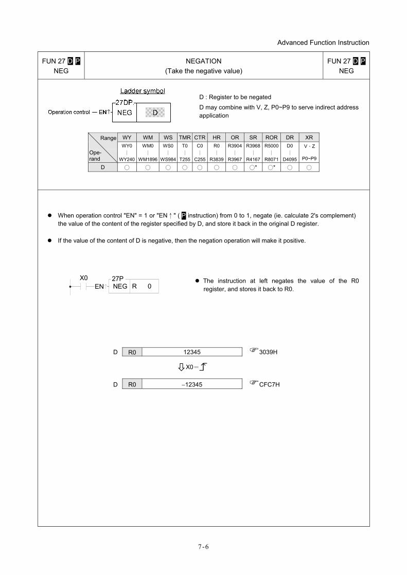
Advanced Function Instruction
7-6
FUN 27 D P NEG
NEGATION (Take the negative value)
FUN 27 D PNEG
D : Register to be negated
D may combine with V, Z, P0~P9 to serve indirect address application
WY WM WS TMR CTR HR OR SR ROR DR XR Range
Ope- rand
WY0 ∣
WY240
WM0 ∣
WM1896
WS0∣
WS984
T0∣
T255
C0∣
C255
R0 ∣
R3839
R3904∣
R3967
R3968∣
R4167
R5000∣
R8071
D0 ∣
D4095
V、Z P0~P9
D ○ ○ ○ ○ ○ ○ ○ ○* ○* ○ ○
When operation control "EN" = 1 or "EN↑" ( P instruction) from 0 to 1, negate (ie. calculate 2's complement) the value of the content of the register specified by D, and store it back in the original D register.
If the value of the content of D is negative, then the negation operation will make it positive.
R 0X0
EN27PNEG
The instruction at left negates the value of the R0 register, and stores it back to R0.
D R0 12345 3039H
X0=
D R0 −12345 CFC7H
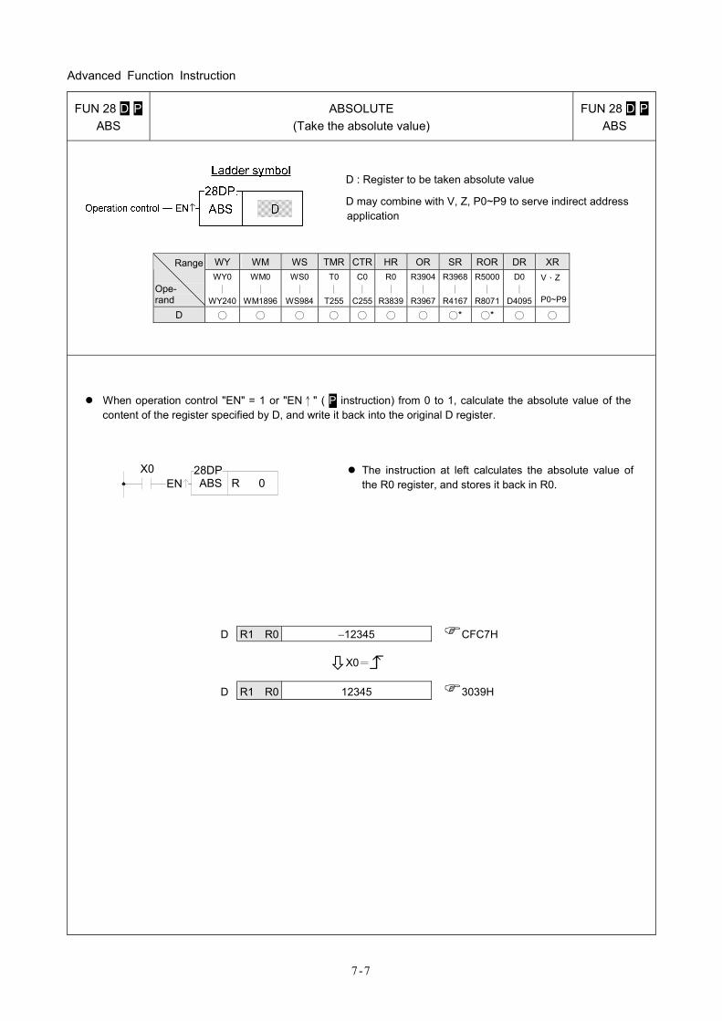
Advanced Function Instruction
7-7
FUN 28 D P ABS
ABSOLUTE (Take the absolute value)
FUN 28 D PABS
D : Register to be taken absolute value
D may combine with V, Z, P0~P9 to serve indirect address application
WY WM WS TMR CTR HR OR SR ROR DR XR Range
Ope- rand
WY0 ∣
WY240
WM0 ∣
WM1896
WS0∣
WS984
T0 ∣
T255
C0∣
C255
R0 ∣
R3839
R3904∣
R3967
R3968∣
R4167
R5000∣
R8071
D0 ∣
D4095
V、Z P0~P9
D ○ ○ ○ ○ ○ ○ ○ ○* ○* ○ ○
When operation control "EN" = 1 or "EN↑" ( P instruction) from 0 to 1, calculate the absolute value of the content of the register specified by D, and write it back into the original D register.
R 0X0
EN28DPABS
The instruction at left calculates the absolute value of the R0 register, and stores it back in R0.
D R1 R0 −12345 CFC7H
X0=
D R1 R0 12345 3039H
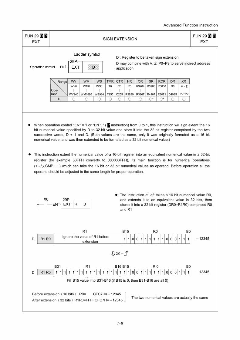
Advanced Function Instruction
7-8
FUN 29 D P EXT
SIGN EXTENSION FUN 29 D P
EXT
D : Register to be taken sign extension
D may combine with V, Z, P0~P9 to serve indirect address application
WY WM WS TMR CTR HR OR SR ROR DR XR Range
Ope- rand
WY0 ∣
WY240
WM0 ∣
WM1896
WS0 ∣
WS984
T0∣
T255
C0∣
C255
R0 ∣
R3839
R3904∣
R3967
R3968∣
R4167
R5000∣
R8071
D0 ∣
D4095
V、Z
P0~P9
D ○ ○ ○ ○ ○ ○ ○ ○* ○* ○ ○
When operation control "EN" = 1 or "EN↑" ( P instruction) from 0 to 1, this instruction will sign extent the 16 bit numerical value specified by D to 32-bit value and store it into the 32-bit register comprised by the two successive words, D + 1 and D. (Both values are the same, only it was originally formated as a 16 bit numerical value, and was then extended to be formated as a 32 bit numerical value.)
This instruction extent the numerical value of a 16-bit register into an equivalent numerical value in a 32-bit register (for example 33FFH converts to 000033FFH), Its main function is for numerical operations (+,-,*,/,CMP......) which can take the 16 bit or 32 bit numerical values as operand. Before operation all the operand should be adjusted to the same length for proper operation.
R 0X0
EN29PEXT
The instruction at left takes a 16 bit numerical value R0, and extends it to an equivalent value in 32 bits, then stores it into a 32 bit register (DR0=R1R0) comprised R0 and R1
R1 B15 R0 B0
D R1 R0 Ignore the value of R1 before extension
1 1 0 0 1 1 1 1 1 1 0 0 0 1 1 1 -12345
X0=
B31 R1 B16 B15 R 0 B0 D R1 R0 1 1 1 1 1 1 1 1 1 1 1 1 1 1 1 1 1 1 0 0 1 1 1 1 1 1 0 0 0 1 1 1 -12345
Fill B15 value into B31-B16,(if B15 is 0, then B31-B16 are all 0)
Before extension(16 bits) R0= CFC7H=−12345
After extension(32 bits)R1R0=FFFFCFC7H=−12345 The two numerical values are actually the same
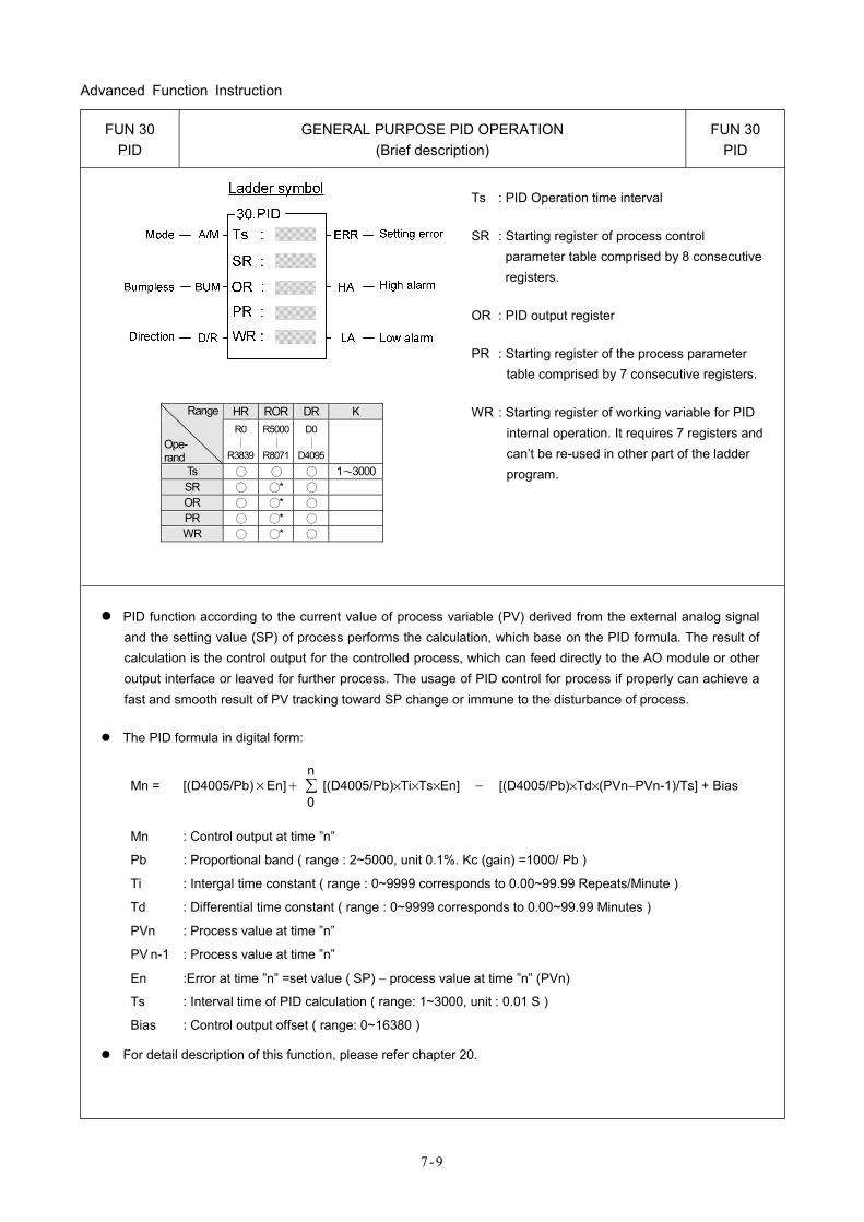
Advanced Function Instruction
7-9
FUN 30 PID
GENERAL PURPOSE PID OPERATION (Brief description)
FUN 30 PID
Ts : PID Operation time interval
SR : Starting register of process control parameter table comprised by 8 consecutive registers.
OR : PID output register
PR : Starting register of the process parameter table comprised by 7 consecutive registers.
WR : Starting register of working variable for PID internal operation. It requires 7 registers and can’t be re-used in other part of the ladder program.
PID function according to the current value of process variable (PV) derived from the external analog signal and the setting value (SP) of process performs the calculation, which base on the PID formula. The result of calculation is the control output for the controlled process, which can feed directly to the AO module or other output interface or leaved for further process. The usage of PID control for process if properly can achieve a fast and smooth result of PV tracking toward SP change or immune to the disturbance of process.
The PID formula in digital form:
Mn = [(D4005/Pb)×En]+ ∑0
n [(D4005/Pb)×Ti×Ts×En] − [(D4005/Pb)×Td×(PVn−PVn-1)/Ts] + Bias
Mn : Control output at time ”n”
Pb : Proportional band ( range : 2~5000, unit 0.1%. Kc (gain) =1000/ Pb )
Ti : Intergal time constant ( range : 0~9999 corresponds to 0.00~99.99 Repeats/Minute )
Td : Differential time constant ( range : 0~9999 corresponds to 0.00~99.99 Minutes )
PVn : Process value at time ”n”
PV n-1 : Process value at time ”n”
En :Error at time ”n” =set value ( SP) − process value at time ”n” (PVn)
Ts : Interval time of PID calculation ( range: 1~3000, unit : 0.01 S )
Bias : Control output offset ( range: 0~16380 )
For detail description of this function, please refer chapter 20.
HR ROR DR K Range
Ope- rand
R0 ∣
R3839
R5000 ∣
R8071
D0 ∣
D4095
Ts ○ ○ ○ 1~3000SR ○ ○* ○ OR ○ ○* ○ PR ○ ○* ○ WR ○ ○* ○
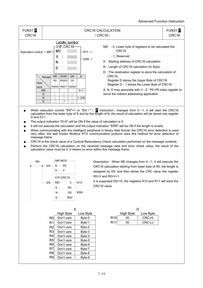
Advanced Function Instruction
7-10
FUN31 P CRC16
CRC16 CALCULATION (CRC16)
FUN31 P CRC16
HR ROR DR K Range
Ope- rand
R0 ∣
R3839
R5000 ∣
R8071
D0 ∣
D4095
MD 0~1 S ○ ○ ○ N ○ ○ ○ 1~256D ○ ○* ○
MD :0, Lower byte of registers to be calculated the CRC16
:1, Reserved
S:Starting address of CRC16 calculation
N:Length of CRC16 calculation (In Byte)
D:The destination register to store the calculation of CRC16, Register D stores the Upper Byte of CRC16 Register D+1 stores the Lower Byte of CRC16
S, N, D may associate with V、Z、P0~P9 index register to serve the indirect addressing application
● When execution control "EN"=1 or "EN↑"( P instruction)changes from 0→1, it will start the CRC16 calculation from the lower byte of S and by the length of N, the result of calculation will be stored into register D and D+1.
● The output indication "D=0" will be ON if the value of calculation is 0. ● It will not execute the calculation and the output indication "ERR" will be ON if the length is invalid. ● When communicating with the intelligent peripheral in binary data fromat, the CRC16 error detection is used
very often; the well known Modbus RTU communication protocol uses this method for error detection of message frame.
● CRC16 is the check value of a Cyclical Redundancy Check calculation performed on the message contents. ● Perform the CRC16 calculation on the received message data and error check value, the result of the
calculation value must be 0, it means no error within this message frame.
S :
D :
D0
V
08P.MOV
MD:
S :
N :
0
R0
D0
31P.CRC16
D : R0V
M0EN
EN
ERR
D=0
S D High Byte Low Byte High Byte Low Byte
R0 Don’t care Byte-0 R10 00 CRC-Hi R1 Don’t care Byte-1 R11 00 CRC-Lo R2 Don’t care Byte-2 R3 Don’t care Byte-3 R4 Don’t care Byte-4 R5 Don’t care Byte-5 R6 Don’t care Byte-6 R7 Don’t care Byte-7 R8 Don’t care Byte-8 R9 Don’t care Byte-9
Description:When M0 changes from 0→1, it will execute the CRC16 calculation starting from lower byte of R0, the length is assigned by D0, and then stores the CRC value into register R0+V and R0+V+1. It is supposed D0=10, the registers R10 and R11 will store the CRC16 value.
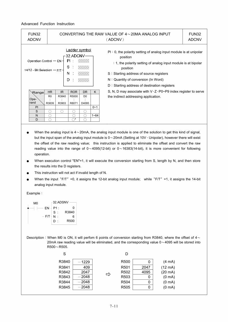
Advanced Function Instruction
7-11
FUN32 ADCNV
CONVERTING THE RAW VALUE OF 4~20MA ANALOG INPUT (ADCNV)
FUN32 ADCNV
HR IR ROR DR K Range Ope- rand
R0 ∣
R3839
R3840 ∣
R3903
R5000 ∣
R8071
D0 ∣
D4095
Pl 0~1S ○ ○ ○ ○ N ○ ○ ○ 1~64D ○ ○* ○
Pl:0, the polarity setting of analog input module is at unipolar position
:1, the polarity setting of analog input module is at bipolar position
S:Starting address of source registers
N:Quantity of conversion (In Word)
D:Starting address of destination registers
S, N, D may associate with V、Z、P0~P9 index register to serve the indirect addressing application.
● When the analog input is 4~20mA, the analog input module is one of the solution to get this kind of signal, but the input span of the analog input module is 0~20mA (Setting at 10V、Unipolar), however there will exist the offset of the raw reading value; this instruction is applied to eliminate the offset and convert the raw reading value into the range of 0~4095(12-bit) or 0~16383(14-bit), it is more convenient for following operation.
● When execution control "EN"=1, it will execute the conversion starting from S, length by N, and then store the results into the D registers.
● This instruction will not act if invalid length of N.
● When the input〝F/T〞=0, it assigns the 12-bit analog input module; while〝F/T〞=1, it assigns the 14-bit analog input module.
Example:
M0EN
S :N :D :
R38406
R500
32.ADSNV
P1 : 0
F/T
Description:When M0 is ON, it will perfom 6 points of conversion starting from R3840, where the offset of 4~
20mA raw reading value will be eliminated, and the corresponding value 0~4095 will be stored into R500~R505.
S D
R3840 -1229 R500 0 (4 mA) R3841 409 R501 2047 (12 mA) R3842 2047 R502 4095 (20 mA) R3843 -2048 R503 0 (0 mA) R3844 -2048 R504 0 (0 mA) R3845 -2048
R505 0 (0 mA)
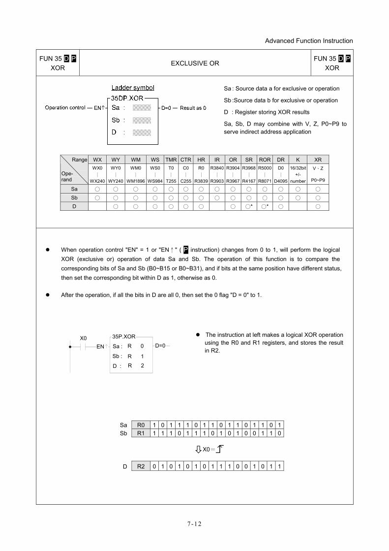
Advanced Function Instruction
7-12
FUN 35 D P XOR
EXCLUSIVE OR FUN 35 D P
XOR
Sa : Source data a for exclusive or operation
Sb :Source data b for exclusive or operation
D : Register storing XOR results
Sa, Sb, D may combine with V, Z, P0~P9 to serve indirect address application
WX WY WM WS TMR CTR HR IR OR SR ROR DR K XR Range
Ope- rand
WX0 ∣
WX240
WY0 ∣
WY240
WM0 ∣
WM1896
WS0 ∣
WS984
T0∣
T255
C0∣
C255
R0∣
R3839
R3840∣
R3903
R3904∣
R3967
R3968∣
R4167
R5000∣
R8071
D0 ∣
D4095
16/32bit +/-
number
V、Z
P0~P9
Sa ○ ○ ○ ○ ○ ○ ○ ○ ○ ○ ○ ○ ○ ○ Sb ○ ○ ○ ○ ○ ○ ○ ○ ○ ○ ○ ○ ○ ○ D ○ ○ ○ ○ ○ ○ ○ ○* ○* ○ ○
When operation control "EN" = 1 or "EN↑" ( P instruction) changes from 0 to 1, will perform the logical XOR (exclusive or) operation of data Sa and Sb. The operation of this function is to compare the corresponding bits of Sa and Sb (B0~B15 or B0~B31), and if bits at the same position have different status, then set the corresponding bit within D as 1, otherwise as 0.
After the operation, if all the bits in D are all 0, then set the 0 flag "D = 0" to 1.
X0EN Sa :
Sb :
D :
R 0
R 2
35P.XORD=0
R 1
The instruction at left makes a logical XOR operation using the R0 and R1 registers, and stores the result in R2.
Sa R0 1 0 1 1 1 0 1 1 0 1 1 0 1 1 0 1 Sb R1 1 1 1 0 1 1 1 0 1 0 1 0 0 1 1 0
X0=
D R2 0 1 0 1 0 1 0 1 1 1 0 0 1 0 1 1
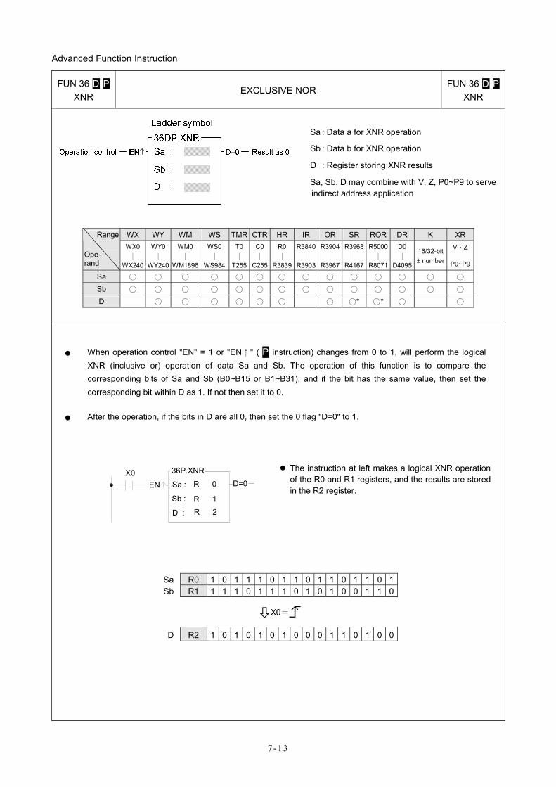
Advanced Function Instruction
7-13
FUN 36 D P XNR
EXCLUSIVE NOR FUN 36 D P
XNR
Sa : Data a for XNR operation
Sb : Data b for XNR operation
D : Register storing XNR results
Sa, Sb, D may combine with V, Z, P0~P9 to serve indirect address application
WX WY WM WS TMR CTR HR IR OR SR ROR DR K XRRange
Ope- rand
WX0 ∣
WX240
WY0∣
WY240
WM0 ∣
WM1896
WS0 ∣
WS984
T0∣
T255
C0∣
C255
R0 ∣
R3839
R3840∣
R3903
R3904∣
R3967
R3968∣
R4167
R5000∣
R8071
D0 ∣
D4095
16/32-bit ± number
V、Z
P0~P9
Sa ○ ○ ○ ○ ○ ○ ○ ○ ○ ○ ○ ○ ○ ○ Sb ○ ○ ○ ○ ○ ○ ○ ○ ○ ○ ○ ○ ○ ○ D ○ ○ ○ ○ ○ ○ ○ ○* ○* ○ ○
● When operation control "EN" = 1 or "EN↑" ( P instruction) changes from 0 to 1, will perform the logical XNR (inclusive or) operation of data Sa and Sb. The operation of this function is to compare the corresponding bits of Sa and Sb (B0~B15 or B1~B31), and if the bit has the same value, then set the corresponding bit within D as 1. If not then set it to 0.
● After the operation, if the bits in D are all 0, then set the 0 flag "D=0" to 1.
X0EN Sa :
Sb :
D :
R 0
R 2
36P.XNRD=0
R 1
The instruction at left makes a logical XNR operation of the R0 and R1 registers, and the results are stored in the R2 register.
Sa R0 1 0 1 1 1 0 1 1 0 1 1 0 1 1 0 1 Sb R1 1 1 1 0 1 1 1 0 1 0 1 0 0 1 1 0
X0=
D R2 1 0 1 0 1 0 1 0 0 0 1 1 0 1 0 0
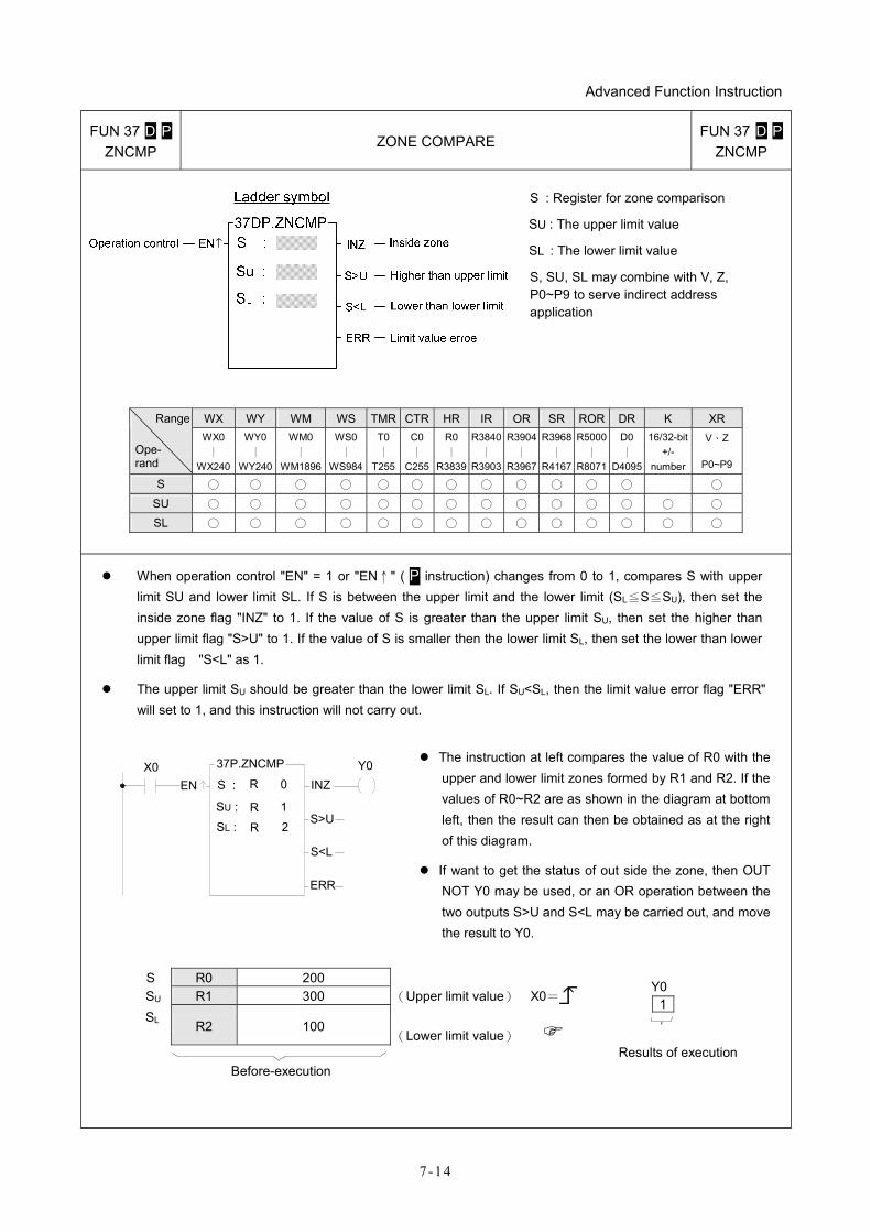
Advanced Function Instruction
7-14
FUN 37 D P ZNCMP
ZONE COMPARE FUN 37 D P
ZNCMP
S : Register for zone comparison
SU : The upper limit value
SL : The lower limit value
S, SU, SL may combine with V, Z, P0~P9 to serve indirect address application
WX WY WM WS TMR CTR HR IR OR SR ROR DR K XR Range
Ope- rand
WX0 ∣
WX240
WY0∣
WY240
WM0 ∣
WM1896
WS0 ∣
WS984
T0∣
T255
C0∣
C255
R0∣
R3839
R3840∣
R3903
R3904∣
R3967
R3968∣
R4167
R5000∣
R8071
D0 ∣
D4095
16/32-bit +/-
number
V、Z
P0~P9
S ○ ○ ○ ○ ○ ○ ○ ○ ○ ○ ○ ○ ○ SU ○ ○ ○ ○ ○ ○ ○ ○ ○ ○ ○ ○ ○ ○ SL ○ ○ ○ ○ ○ ○ ○ ○ ○ ○ ○ ○ ○ ○
When operation control "EN" = 1 or "EN↑" ( P instruction) changes from 0 to 1, compares S with upper limit SU and lower limit SL. If S is between the upper limit and the lower limit (SL≦S≦SU), then set the inside zone flag "INZ" to 1. If the value of S is greater than the upper limit SU, then set the higher than upper limit flag "S>U" to 1. If the value of S is smaller then the lower limit SL, then set the lower than lower limit flag "S<L" as 1.
The upper limit SU should be greater than the lower limit SL. If SU<SL, then the limit value error flag "ERR" will set to 1, and this instruction will not carry out.
X0EN S :
SU :
R
R
0
1
37P.ZNCMP
INZ
S>U
S<L
Y0
SL : R 2
ERR
The instruction at left compares the value of R0 with the upper and lower limit zones formed by R1 and R2. If the values of R0~R2 are as shown in the diagram at bottom left, then the result can then be obtained as at the right of this diagram.
If want to get the status of out side the zone, then OUT NOT Y0 may be used, or an OR operation between the two outputs S>U and S<L may be carried out, and move the result to Y0.
S R0 200 SU R1 300 (Upper limit value) X0= SL R2 100
(Lower limit value)
Y0 1
Before-execution Results of execution
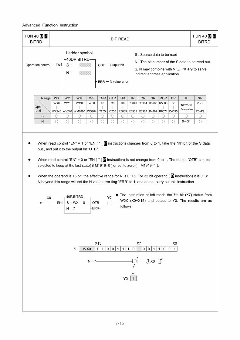
Advanced Function Instruction
7-15
FUN 40 D P BITRD
BIT READ FUN 40 D P
BITRD
S :ENOperation control
Ladder symbol 40DP.BITRD
N :
OBT Output bit
ERR N value error
S : Source data to be read
N : The bit number of the S data to be read out.
S, N may combine with V, Z, P0~P9 to serve indirect address application
WX WY WM WS TMR CTR HR IR OR SR ROR DR K XRRange
Ope- rand
WX0 ∣
WX240
WY0 ∣
WY240
WM0 ∣
WM1896
WS0 ∣
WS984
T0 ∣
T255
C0 ∣
C255
R0 ∣
R3839
R3840∣
R3903
R3904∣
R3967
R3968∣
R4167
R5000∣
R8071
D0 ∣
D4095
16/32-bit +/- number
V、Z
P0~P9
S ○ ○ ○ ○ ○ ○ ○ ○ ○ ○ ○ ○ ○ ○ N ○ ○ ○ ○ ○ ○ ○ ○ ○ ○ ○ ○ 0~31 ○
When read control "EN" = 1 or "EN↑" ( P instruction) changes from 0 to 1, take the Nth bit of the S data out , and put it to the output bit "OTB".
When read control "EN" = 0 or "EN↑" ( P instruction) is not change from 0 to 1, The output “OTB” can be selected to keep at the last state( if M1919=0 ) or set to zero ( if M1919=1 ).
When the operand is 16 bit, the effective range for N is 0~15. For 32 bit operand ( D instruction) it is 0~31. N beyond this range will set the N value error flag "ERR" to 1, and do not carry out this instruction.
X0S :
Y0EN
40P.BITRD
N : 7
WX 0 OTBERR
The instruction at left reads the 7th bit (X7) status from WX0 (X0~X15) and output to Y0. The results are as follows:
X15 X7 X0 S WX0 1 1 0 0 1 1 1 0 1 0 0 1 1 0 0 1
N=7────────── X0=
Y0 1
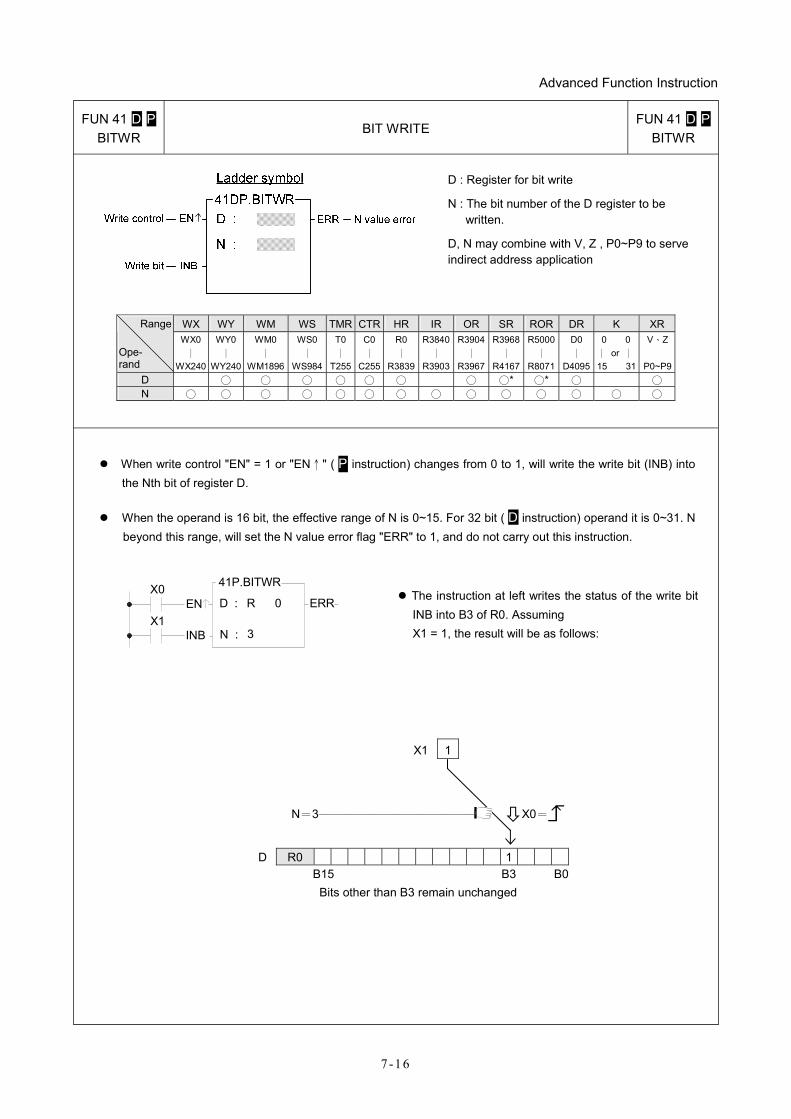
Advanced Function Instruction
7-16
FUN 41 D P BITWR
BIT WRITE FUN 41 D P
BITWR
D : Register for bit write
N : The bit number of the D register to be written.
D, N may combine with V, Z , P0~P9 to serve indirect address application
WX WY WM WS TMR CTR HR IR OR SR ROR DR K XRRange
Ope- rand
WX0 ∣
WX240
WY0∣
WY240
WM0 ∣
WM1896
WS0 ∣
WS984
T0∣
T255
C0∣
C255
R0 ∣
R3839
R3840∣
R3903
R3904∣
R3967
R3968∣
R4167
R5000∣
R8071
D0 ∣
D4095
0 0 ∣ or ∣ 15 31
V、Z
P0~P9D ○ ○ ○ ○ ○ ○ ○ ○* ○* ○ ○ N ○ ○ ○ ○ ○ ○ ○ ○ ○ ○ ○ ○ ○ ○
When write control "EN" = 1 or "EN↑" ( P instruction) changes from 0 to 1, will write the write bit (INB) into the Nth bit of register D.
When the operand is 16 bit, the effective range of N is 0~15. For 32 bit ( D instruction) operand it is 0~31. N beyond this range, will set the N value error flag "ERR" to 1, and do not carry out this instruction.
EN
41P.BITWR
D : R 0 ERRX0
3N :X1
INB
The instruction at left writes the status of the write bit INB into B3 of R0. Assuming X1 = 1, the result will be as follows:
X1 1
N=3───────────── X0=
D R0 1 B15 B3 B0 Bits other than B3 remain unchanged
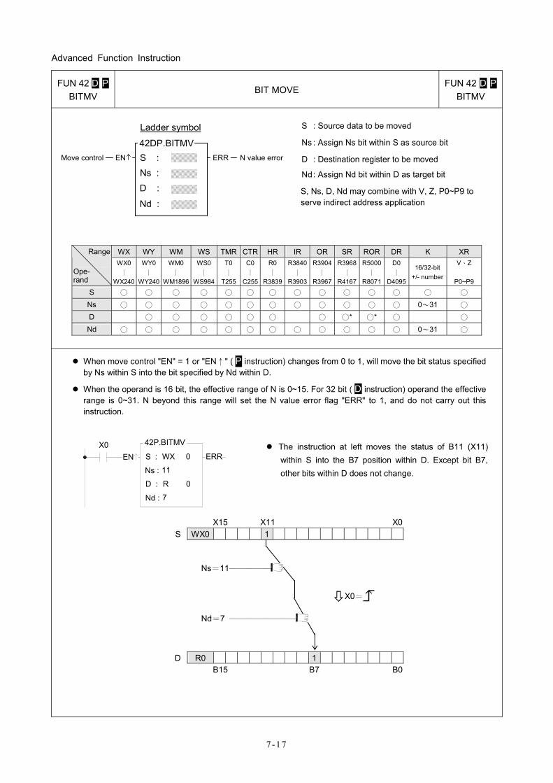
Advanced Function Instruction
7-17
FUN 42 D P BITMV
BIT MOVE FUN 42 D P
BITMV
S :
D :
ENMove control
Ladder symbol
42DP.BITMV
Ns :
ERR N value error
Nd :
S : Source data to be moved
Ns : Assign Ns bit within S as source bit
D : Destination register to be moved
Nd : Assign Nd bit within D as target bit
S, Ns, D, Nd may combine with V, Z, P0~P9 to serve indirect address application
WX WY WM WS TMR CTR HR IR OR SR ROR DR K XR Range
Ope- rand
WX0 ∣
WX240
WY0 ∣
WY240
WM0 ∣
WM1896
WS0 ∣
WS984
T0 ∣
T255
C0∣
C255
R0 ∣
R3839
R3840∣
R3903
R3904∣
R3967
R3968∣
R4167
R5000∣
R8071
D0 ∣
D4095
16/32-bit +/- number
V、Z
P0~P9
S ○ ○ ○ ○ ○ ○ ○ ○ ○ ○ ○ ○ ○ ○ Ns ○ ○ ○ ○ ○ ○ ○ ○ ○ ○ ○ ○ 0~31 ○ D ○ ○ ○ ○ ○ ○ ○ ○* ○* ○ ○ Nd ○ ○ ○ ○ ○ ○ ○ ○ ○ ○ ○ ○ 0~31 ○
When move control "EN" = 1 or "EN↑" ( P instruction) changes from 0 to 1, will move the bit status specified by Ns within S into the bit specified by Nd within D.
When the operand is 16 bit, the effective range of N is 0~15. For 32 bit ( D instruction) operand the effective range is 0~31. N beyond this range will set the N value error flag "ERR" to 1, and do not carry out this instruction.
X0EN S :
Ns : 11
WX 0
42P.BITMV
ERR
D :
Nd :
R 0
7
The instruction at left moves the status of B11 (X11) within S into the B7 position within D. Except bit B7, other bits within D does not change.
X15 X11 X0 S WX0 1
Ns=11─────
X0=
Nd=7 ────────
D R0 1 B15 B7 B0
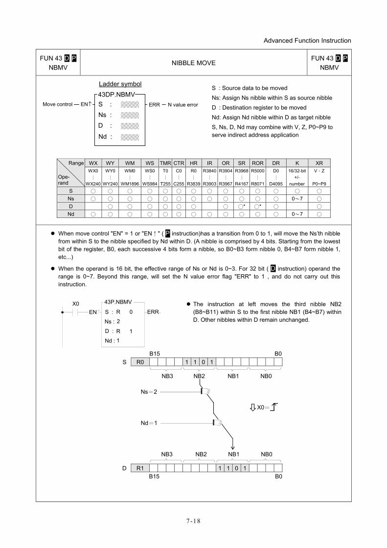
Advanced Function Instruction
7-18
FUN 43 D P NBMV
NIBBLE MOVE FUN 43 D P
NBMV
S :
D :
ENMove control
Ladder symbol 43DP.NBMV
Ns :ERR N value error
Nd :
S : Source data to be moved
Ns: Assign Ns nibble within S as source nibble
D : Destination register to be moved
Nd: Assign Nd nibble within D as target nibble
S, Ns, D, Nd may combine with V, Z, P0~P9 to serve indirect address application
WX WY WM WS TMR CTR HR IR OR SR ROR DR K XR Range
Ope- rand
WX0 ∣
WX240
WY0∣
WY240
WM0 ∣
WM1896
WS0 ∣
WS984
T0∣
T255
C0∣
C255
R0∣
R3839
R3840∣
R3903
R3904∣
R3967
R3968∣
R4167
R5000∣
R8071
D0 ∣
D4095
16/32-bit +/-
number
V、Z
P0~P9S ○ ○ ○ ○ ○ ○ ○ ○ ○ ○ ○ ○ ○ ○
Ns ○ ○ ○ ○ ○ ○ ○ ○ ○ ○ ○ ○ 0~7 ○ D ○ ○ ○ ○ ○ ○ ○ ○* ○* ○ ○ Nd ○ ○ ○ ○ ○ ○ ○ ○ ○ ○ ○ ○ 0~7 ○
When move control "EN" = 1 or "EN↑" ( P instruction)has a transition from 0 to 1, will move the Ns’th nibble from within S to the nibble specified by Nd within D. (A nibble is comprised by 4 bits. Starting from the lowest bit of the register, B0, each successive 4 bits form a nibble, so B0~B3 form nibble 0, B4~B7 form nibble 1, etc...)
When the operand is 16 bit, the effective range of Ns or Nd is 0~3. For 32 bit ( D instruction) operand the range is 0~7. Beyond this range, will set the N value error flag "ERR" to 1 , and do not carry out this instruction.
X0EN S :
Ns :
ERR
D :
Nd :
43P.NBMV
1R 1
2
R 0
The instruction at left moves the third nibble NB2 (B8~B11) within S to the first nibble NB1 (B4~B7) within D. Other nibbles within D remain unchanged.
B15 B0 S R0 1 1 0 1
NB3 NB2 NB1 NB0
Ns=2 ───────
X0=
Nd=1 ─────────
NB3 NB2 NB1 NB0
D R1 1 1 0 1 B15 B0
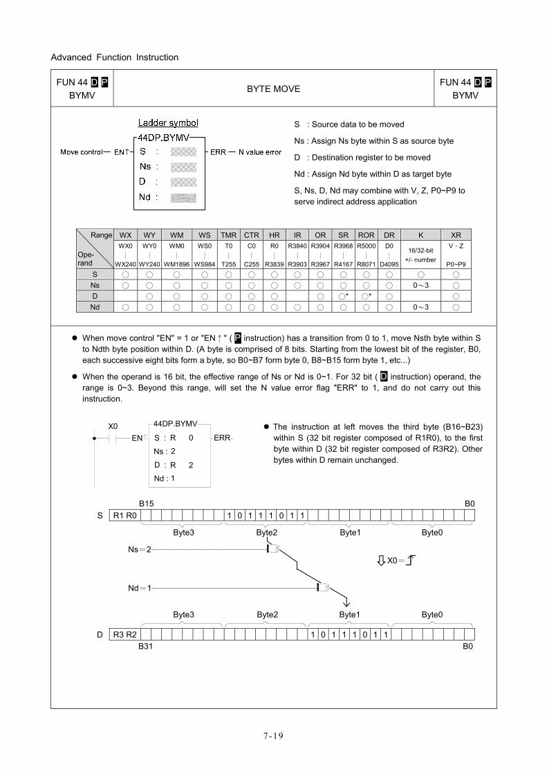
Advanced Function Instruction
7-19
FUN 44 D P BYMV
BYTE MOVE FUN 44 D P
BYMV
S : Source data to be moved
Ns : Assign Ns byte within S as source byte
D : Destination register to be moved
Nd : Assign Nd byte within D as target byte
S, Ns, D, Nd may combine with V, Z, P0~P9 to serve indirect address application
WX WY WM WS TMR CTR HR IR OR SR ROR DR K XR Range
Ope- rand
WX0 ∣
WX240
WY0 ∣
WY240
WM0 ∣
WM1896
WS0 ∣
WS984
T0 ∣
T255
C0 ∣
C255
R0 ∣
R3839
R3840∣
R3903
R3904∣
R3967
R3968∣
R4167
R5000∣
R8071
D0 ∣
D4095
16/32-bit +/- number
V、Z
P0~P9S ○ ○ ○ ○ ○ ○ ○ ○ ○ ○ ○ ○ ○ ○ Ns ○ ○ ○ ○ ○ ○ ○ ○ ○ ○ ○ ○ 0~3 ○ D ○ ○ ○ ○ ○ ○ ○ ○* ○* ○ ○
Nd ○ ○ ○ ○ ○ ○ ○ ○ ○ ○ ○ ○ 0~3 ○
When move control "EN" = 1 or "EN↑" ( P instruction) has a transition from 0 to 1, move Nsth byte within S to Ndth byte position within D. (A byte is comprised of 8 bits. Starting from the lowest bit of the register, B0, each successive eight bits form a byte, so B0~B7 form byte 0, B8~B15 form byte 1, etc...)
When the operand is 16 bit, the effective range of Ns or Nd is 0~1. For 32 bit ( D instruction) operand, the range is 0~3. Beyond this range, will set the N value error flag "ERR" to 1, and do not carry out this instruction.
X0EN S :
Ns : 2
R 0 ERR
D :
Nd : 1
44DP.BYMV
R 2
The instruction at left moves the third byte (B16~B23) within S (32 bit register composed of R1R0), to the first byte within D (32 bit register composed of R3R2). Other bytes within D remain unchanged.
B15 B0 S R1 R0 1 0 1 1 1 0 1 1
Byte3 Byte2 Byte1 Byte0
Ns=2──────────────
X0=
Nd=1────────────────────
Byte3 Byte2 Byte1 Byte0
D R3 R2 1 0 1 1 1 0 1 1 B31 B0
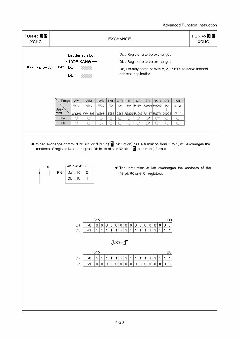
Advanced Function Instruction
7-20
FUN 45 D P XCHG
EXCHANGE FUN 45 D P
XCHG
Da : Register a to be exchanged
Db : Register b to be exchanged
Da, Db may combine with V, Z, P0~P9 to serve indirect address application
WY WM WS TMR CTR HR OR SR ROR DR XR Range
Ope- rand
WY0 ∣
WY240
WM0 ∣
WM1896
WS0∣
WS984
T0∣
T255
C0∣
C255
R0∣
R3839
R3904∣
R3967
R3968∣
R4167
R5000∣
R8071
D0∣
D4095
V、Z
P0~P9
Da ○ ○ ○ ○ ○ ○ ○ ○* ○* ○ ○ Db ○ ○ ○ ○ ○ ○ ○ ○* ○* ○ ○
When exchange control "EN" = 1 or "EN↑" ( P instruction) has a transition from 0 to 1, will exchanges the contents of register Da and register Db in 16 bits or 32 bits ( D instruction) format.
X0EN
45P.XCHG
Da :Db : R 1
R 0
The instruction at left exchanges the contents of the 16-bit R0 and R1 registers.
B15 B0 Da R0 0 0 0 0 0 0 0 0 0 0 0 0 0 0 0 0 Db R1 1 1 1 1 1 1 1 1 1 1 1 1 1 1 1 1
X0=
B15 B0 Da R0 1 1 1 1 1 1 1 1 1 1 1 1 1 1 1 1 Db R1 0 0 0 0 0 0 0 0 0 0 0 0 0 0 0 0
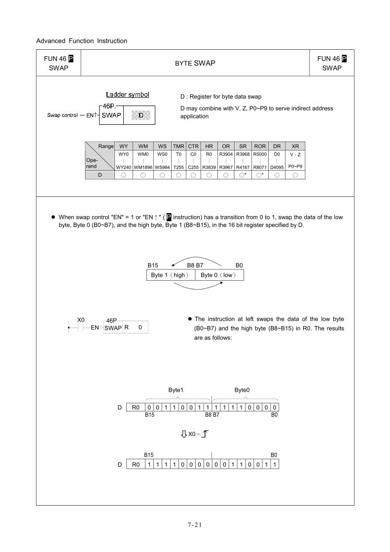
Advanced Function Instruction
7-21
FUN 46 P SWAP
BYTE SWAP FUN 46 P
SWAP
D : Register for byte data swap
D may combine with V, Z, P0~P9 to serve indirect address application
WY WM WS TMR CTR HR OR SR ROR DR XR Range
Ope- rand
WY0 ∣
WY240
WM0 ∣
WM1896
WS0∣
WS984
T0∣
T255
C0∣
C255
R0 ∣
R3839
R3904∣
R3967
R3968∣
R4167
R5000∣
R8071
D0 ∣
D4095
V、Z
P0~P9
D ○ ○ ○ ○ ○ ○ ○ ○* ○* ○ ○
When swap control "EN" = 1 or "EN↑" ( P instruction) has a transition from 0 to 1, swap the data of the low byte, Byte 0 (B0~B7), and the high byte, Byte 1 (B8~B15), in the 16 bit register specified by D.
B15 B8 B7 B0Byte 1(high) Byte 0(low)
X0 46PSWAP R 0EN
The instruction at left swaps the data of the low byte (B0~B7) and the high byte (B8~B15) in R0. The results are as follows:
Byte1 Byte0
D R0 0 0 1 1 0 0 1 1 1 1 1 1 0 0 0 0 B15 B8 B7 B0
X0=
B15 B0 D R0 1 1 1 1 0 0 0 0 0 0 1 1 0 0 1 1
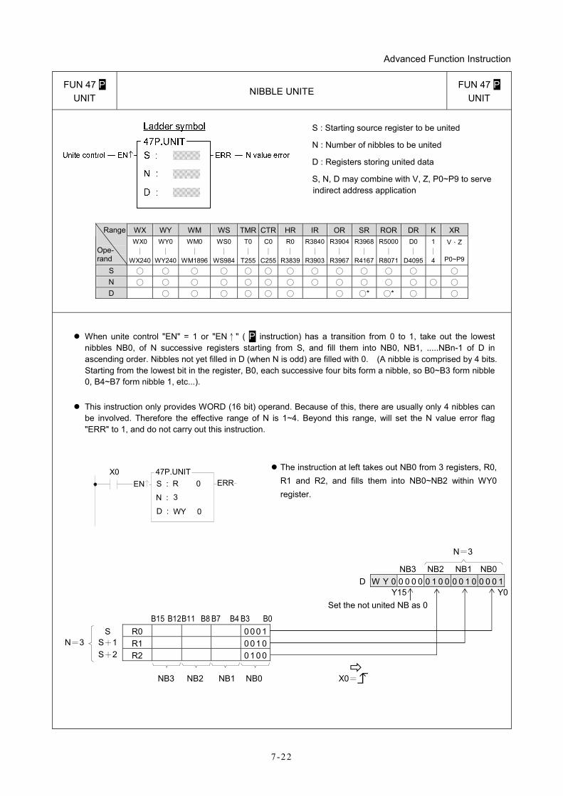
Advanced Function Instruction
7-22
FUN 47 P UNIT
NIBBLE UNITE FUN 47 P
UNIT
S : Starting source register to be united
N : Number of nibbles to be united
D : Registers storing united data
S, N, D may combine with V, Z, P0~P9 to serve indirect address application
WX WY WM WS TMR CTR HR IR OR SR ROR DR K XR Range
Ope- rand
WX0 ∣
WX240
WY0∣
WY240
WM0 ∣
WM1896
WS0 ∣
WS984
T0∣
T255
C0∣
C255
R0 ∣
R3839
R3840∣
R3903
R3904∣
R3967
R3968∣
R4167
R5000 ∣
R8071
D0 ∣
D4095
1 ∣ 4
V、Z
P0~P9
S ○ ○ ○ ○ ○ ○ ○ ○ ○ ○ ○ ○ ○ N ○ ○ ○ ○ ○ ○ ○ ○ ○ ○ ○ ○ ○ ○ D ○ ○ ○ ○ ○ ○ ○ ○* ○* ○ ○
When unite control "EN" = 1 or "EN↑" ( P instruction) has a transition from 0 to 1, take out the lowest nibbles NB0, of N successive registers starting from S, and fill them into NB0, NB1, .....NBn-1 of D in ascending order. Nibbles not yet filled in D (when N is odd) are filled with 0. (A nibble is comprised by 4 bits. Starting from the lowest bit in the register, B0, each successive four bits form a nibble, so B0~B3 form nibble 0, B4~B7 form nibble 1, etc...).
This instruction only provides WORD (16 bit) operand. Because of this, there are usually only 4 nibbles can be involved. Therefore the effective range of N is 1~4. Beyond this range, will set the N value error flag "ERR" to 1, and do not carry out this instruction.
47P.UNIT
WY 0D :
3
R 0S :
N :
X0EN ERR
The instruction at left takes out NB0 from 3 registers, R0, R1 and R2, and fills them into NB0~NB2 within WY0 register.
N=3
NB3 NB2 NB1 NB0 D W Y 0 0 0 0 0 0 1 0 0 0 0 1 0 0 0 0 1
Y15 Y0 Set the not united NB as 0 B15 B12 B11 B8 B7 B4 B3 B0
S R0 0 00 1N=3 S+1 R1 0 01 0 S+2 R2 0 10 0
NB3 NB2 NB1 NB0 X0=
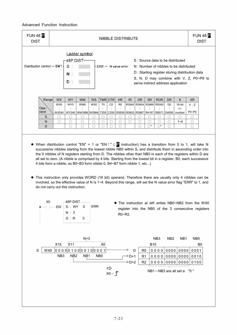
Advanced Function Instruction
7-23
FUN 48 P DIST
NIBBLE DISTRIBUTE FUN 48 P
DIST
S : Source data to be distributed
N : Number of nibbles to be distributed
D : Starting register storing distribution data
S, N, D may combine with V, Z, P0~P9 to serve indirect address application
WX WY WM WS TMR CTR HR IR OR SR ROR DR K XR Range
Ope- rand
WX0 ∣
WX240
WY0 ∣
WY240
WM0 ∣
WM1896
WS0 ∣
WS984
T0∣
T255
C0∣
C255
R0∣
R3839
R3840∣
R3903
R3904∣
R3967
R3968∣
R4167
R5000∣
R8071
D0 ∣
D4095
16-bit +/-
number
V、Z
P0~P9
S ○ ○ ○ ○ ○ ○ ○ ○ ○ ○ ○ ○ ○ ○ N ○ ○ ○ ○ ○ ○ ○ ○ ○ ○ ○ ○ 1~4 ○ D ○ ○ ○ ○ ○ ○ ○ ○* ○* ○ ○
When distribution control "EN" = 1 or "EN↑" ( P instruction) has a transition from 0 to 1, will take N successive nibbles starting from the lowest nibble NB0 within S, and distribute them in ascending order into the 0 nibbles of N registers starting from D. The nibbles other than NB0 in each of the registers within D are all set to zero. (A nibble is comprised by 4 bits. Starting from the lowest bit in a register, B0, each successive 4 bits form a nibble, so B0~B3 form nibble 0, B4~B7 form nibble 1, etc...)
This instruction only provides WORD (16 bit) operand. Therefore there are usually only 4 nibbles can be involved, so the effective value of N is 1~4. Beyond this range, will set the N value error flag "ERR" to 1, and do not carry out this instruction.
X0EN S :
N : 3
ERR
D :
48P.DISTWY 0
R 0
The instruction at left writes NB0~NB2 from the WX0 register into the NB0 of the 3 consecutive registers R0~R2.
N=3 NB3 NB2 NB1 NB0 X15 X11 X0 B15 B0
S WX0 0 0 0 0 0 1 0 0 0 0 1 0 0 0 0 1 D R0 0 0 0 0 0 0 0 0 0 0 0 0 0 0 0 1 NB3 NB2 NB1 NB0 D+1 R1 0 0 0 0 0 0 0 0 0 0 0 0 0 0 1 0 D+2 R2 0 0 0 0 0 0 0 0 0 0 0 0 0 1 0 0 X0=
NB1~NB3 are all set a "0 "
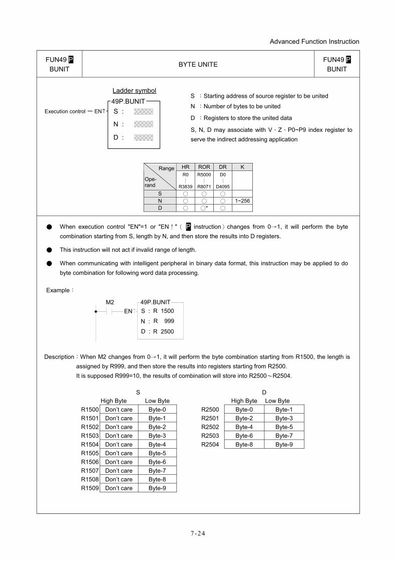
Advanced Function Instruction
7-24
FUN49 P BUNIT
BYTE UNITE FUN49 P
BUNIT
S :
D :
ENExecution control
Ladder symbol 49P.BUNIT
N :
S :Starting address of source register to be united
N :Number of bytes to be united
D :Registers to store the united data
S, N, D may associate with V、Z、P0~P9 index register to serve the indirect addressing application
HR ROR DR K Range
Ope- rand
R0 ∣
R3839
R5000∣
R8071
D0 ∣
D4095
S ○ ○ ○ N ○ ○ ○ 1~256D ○ ○* ○
● When execution control "EN"=1 or "EN↑"( P instruction)changes from 0→1, it will perform the byte combination starting from S, length by N, and then store the results into D registers.
● This instruction will not act if invalid range of length.
● When communicating with intelligent peripheral in binary data format, this instruction may be applied to do byte combination for following word data processing.
Example:
EN S :
N :
D :
M2 49P.BUNITR 1500
R 999
R 2500
Description:When M2 changes from 0→1, it will perform the byte combination starting from R1500, the length is
assigned by R999, and then store the results into registers starting from R2500. It is supposed R999=10, the results of combination will store into R2500~R2504.
S D High Byte Low Byte High Byte Low Byte
R1500 Don’t care Byte-0 R2500 Byte-0 Byte-1 R1501 Don’t care Byte-1 R2501 Byte-2 Byte-3 R1502 Don’t care Byte-2 R2502 Byte-4 Byte-5 R1503 Don’t care Byte-3 R2503 Byte-6 Byte-7 R1504 Don’t care Byte-4 R2504 Byte-8 Byte-9 R1505 Don’t care Byte-5 R1506 Don’t care Byte-6 R1507 Don’t care Byte-7 R1508 Don’t care Byte-8 R1509 Don’t care Byte-9
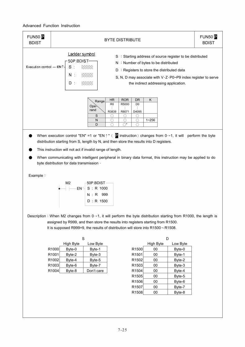
Advanced Function Instruction
7-25
FUN50 P BDIST
BYTE DISTRIBUTE FUN50 P
BDIST
S :Starting address of source register to be distributed
N :Number of bytes to be distributed
D :Registers to store the distributed data
S, N, D may associate with V、Z、P0~P9 index register to serve the indirect addressing application.
HR ROR DR K Range
Ope- rand
R0 ∣
R3839
R5000∣
R8071
D0 ∣
D4095
S ○ ○ ○ N ○ ○ ○ 1~256D ○ ○* ○
● When execution control "EN" =1 or "EN↑"( P instruction)changes from 0→1, it will perform the byte distribution starting from S, length by N, and then store the results into D registers.
● This instruction will not act if invalid range of length.
● When communicating with intelligent peripheral in binary data format, this instruction may be applied to do byte distribution for data transmission。
Example:
M2EN S :
N : R 999
R 100050P.BDIST
D : R 1500
Description:When M2 changes from 0→1, it will perform the byte distribution starting from R1000, the length is
assigned by R999, and then store the results into registers starting from R1500. It is supposed R999=9, the results of distribution will store into R1500~R1508.
S D High Byte Low Byte High Byte Low Byte
R1000 Byte-0 Byte-1 R1500 00 Byte-0 R1001 Byte-2 Byte-3 R1501 00 Byte-1 R1002 Byte-4 Byte-5 R1502 00 Byte-2 R1003 Byte-6 Byte-7 R1503 00 Byte-3 R1004 Byte-8 Don’t care R1504 00 Byte-4
R1505 00 Byte-5 R1506 00 Byte-6 R1507 00 Byte-7
R1508 00 Byte-8
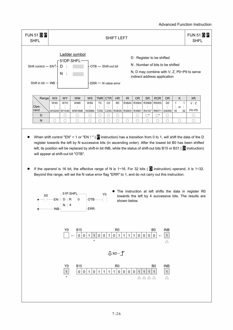
Advanced Function Instruction
7-26
FUN 51 D P SHFL
SHIFT LEFT FUN 51 D P
SHFL
D :ENShift control
Ladder symbol 51DP.SHFL
N :
Shift in bit INB
OTB
ERR
Shift-out bit
N value error
D : Register to be shifted
N : Number of bits to be shifted
N, D may combine with V, Z, P0~P9 to serve indirect address application
WX WY WM WS TMR CTR HR IR OR SR ROR DR K XR Range
Ope- rand
WX0 ∣
WX240
WY0 ∣
WY240
WM0 ∣
WM1896
WS0 ∣
WS984
T0∣
T255
C0∣
C255
R0 ∣
R3839
R3840∣
R3903
R3904∣
R3967
R3968∣
R4167
R5000∣
R8071
D0 ∣
D4095
1 1 ∣ or ∣ 16 32
V、Z
P0~P9
D ○ ○ ○ ○ ○ ○ ○ ○* ○* ○ ○ N ○ ○ ○ ○ ○ ○ ○ ○ ○ ○ ○ ○ ○ ○
When shift control "EN" = 1 or "EN↑" ( P instruction) has a transition from 0 to 1, will shift the data of the D register towards the left by N successive bits (in ascending order). After the lowest bit B0 has been shifted left, its position will be replaced by shift-in bit INB, while the status of shift-out bits B15 or B31 ( D instruction) will appear at shift-out bit "OTB".
If the operand is 16 bit, the effective range of N is 1~16. For 32 bits ( D instruction) operand, it is 1~32. Beyond this range, will set the N value error flag "ERR" to 1, and do not carry out this instruction.
EN
N :
OTBY051P.SHFLX0
INB
D :
4
R 0
ERR
The instruction at left shifts the data in register R0 towards the left by 4 successive bits. The results are shown below.
Y0 B15 R0 B0 INB ← 0 0 1 1 0 0 1 0 1 1 1 1 0 0 0 0 ← 1 * △
X0=
Y0 B15 R0 B0 INB 1 0 0 1 0 1 1 1 1 0 0 0 0 1 1 1 1 1 * △ △ △ △ △
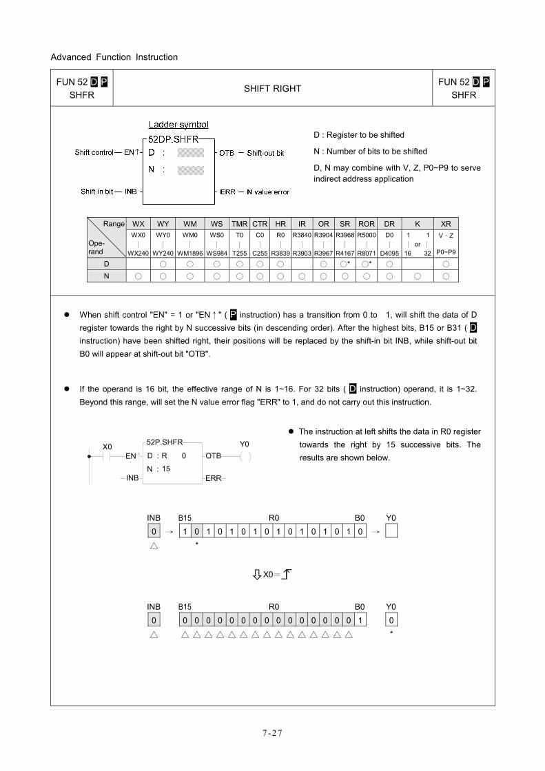
Advanced Function Instruction
7 -27
FUN 52 D P SHFR
SHIFT RIGHT FUN 52 D P
SHFR
D : Register to be shifted
N : Number of bits to be shifted
D, N may combine with V, Z, P0~P9 to serve indirect address application
WX WY WM WS TMR CTR HR IR OR SR ROR DR K XRRange
Ope- rand
WX0 ∣
WX240
WY0 ∣
WY240
WM0 ∣
WM1896
WS0 ∣
WS984
T0∣
T255
C0∣
C255
R0∣
R3839
R3840∣
R3903
R3904∣
R3967
R3968∣
R4167
R5000∣
R8071
D0 ∣
D4095
1 1 ∣ or ∣ 16 32
V、Z
P0~P9
D ○ ○ ○ ○ ○ ○ ○ ○* ○* ○ ○ N ○ ○ ○ ○ ○ ○ ○ ○ ○ ○ ○ ○ ○ ○
When shift control "EN" = 1 or "EN↑" ( P instruction) has a transition from 0 to 1, will shift the data of D register towards the right by N successive bits (in descending order). After the highest bits, B15 or B31 ( D instruction) have been shifted right, their positions will be replaced by the shift-in bit INB, while shift-out bit B0 will appear at shift-out bit "OTB".
If the operand is 16 bit, the effective range of N is 1~16. For 32 bits ( D instruction) operand, it is 1~32. Beyond this range, will set the N value error flag "ERR" to 1, and do not carry out this instruction.
X0EN D :
N : 15
R 0
52P.SHFR
OTBY0
ERRINB
The instruction at left shifts the data in R0 register towards the right by 15 successive bits. The results are shown below.
INB B15 R0 B0 Y0 0 → 1 0 1 0 1 0 1 0 1 0 1 0 1 0 1 0 → △ *
X0=
INB B15 R0 B0 Y0 0 0 0 0 0 0 0 0 0 0 0 0 0 0 0 0 1 0 △ △ △ △ △ △ △ △ △ △ △ △ △ △ △ △ *
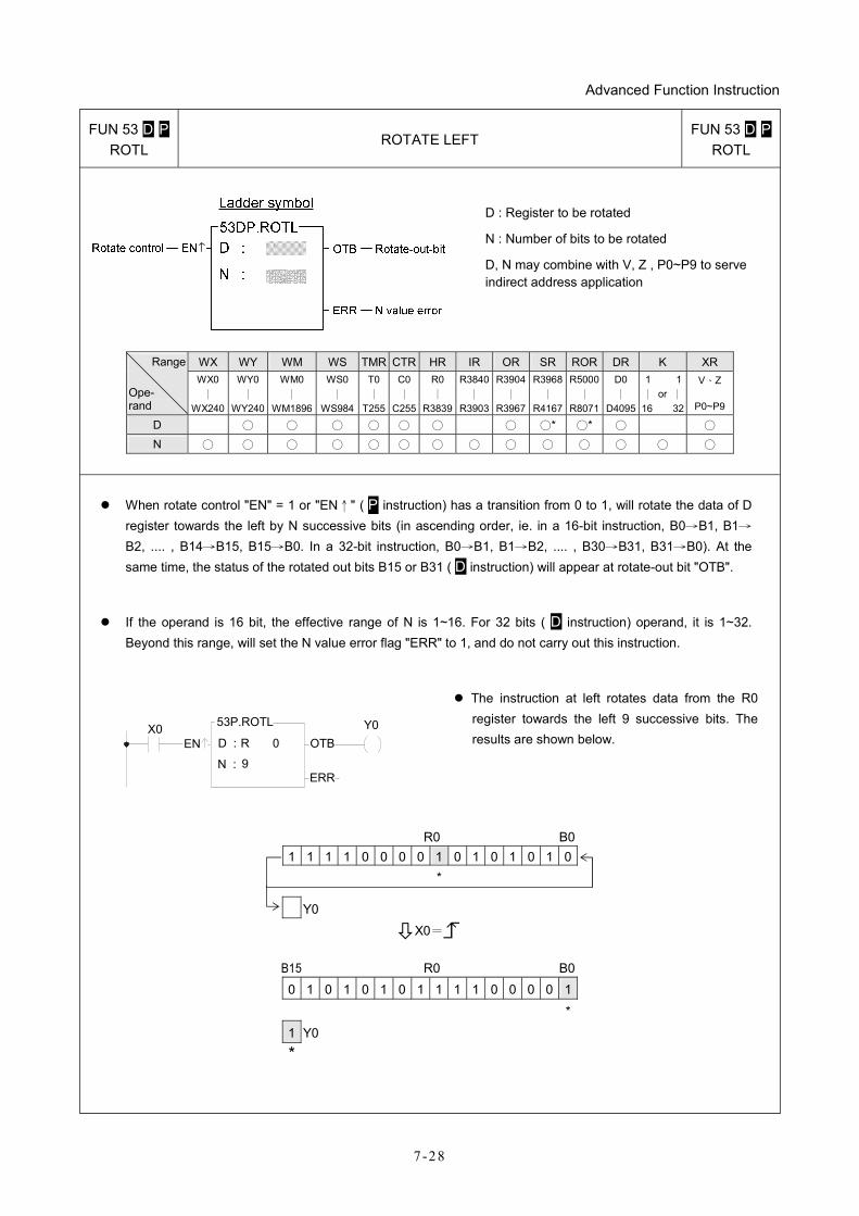
Advanced Function Instruction
7-28
FUN 53 D P ROTL
ROTATE LEFT FUN 53 D P
ROTL
D : Register to be rotated
N : Number of bits to be rotated
D, N may combine with V, Z , P0~P9 to serve indirect address application
WX WY WM WS TMR CTR HR IR OR SR ROR DR K XR Range
Ope- rand
WX0 ∣
WX240
WY0∣
WY240
WM0 ∣
WM1896
WS0 ∣
WS984
T0∣
T255
C0∣
C255
R0 ∣
R3839
R3840∣
R3903
R3904∣
R3967
R3968∣
R4167
R5000∣
R8071
D0 ∣
D4095
1 1 ∣ or ∣ 16 32
V、Z
P0~P9
D ○ ○ ○ ○ ○ ○ ○ ○* ○* ○ ○ N ○ ○ ○ ○ ○ ○ ○ ○ ○ ○ ○ ○ ○ ○
When rotate control "EN" = 1 or "EN↑" ( P instruction) has a transition from 0 to 1, will rotate the data of D register towards the left by N successive bits (in ascending order, ie. in a 16-bit instruction, B0→B1, B1→B2, .... , B14→B15, B15→B0. In a 32-bit instruction, B0→B1, B1→B2, .... , B30→B31, B31→B0). At the same time, the status of the rotated out bits B15 or B31 ( D instruction) will appear at rotate-out bit "OTB".
If the operand is 16 bit, the effective range of N is 1~16. For 32 bits ( D instruction) operand, it is 1~32. Beyond this range, will set the N value error flag "ERR" to 1, and do not carry out this instruction.
X0EN D :
N :
R 0 OTBY0
ERR
53P.ROTL
9
The instruction at left rotates data from the R0 register towards the left 9 successive bits. The results are shown below.
R0 B0 1 1 1 1 0 0 0 0 1 0 1 0 1 0 1 0
*
Y0 X0=
B15 R0 B0 0 1 0 1 0 1 0 1 1 1 1 0 0 0 0 1
*
1 Y0
*
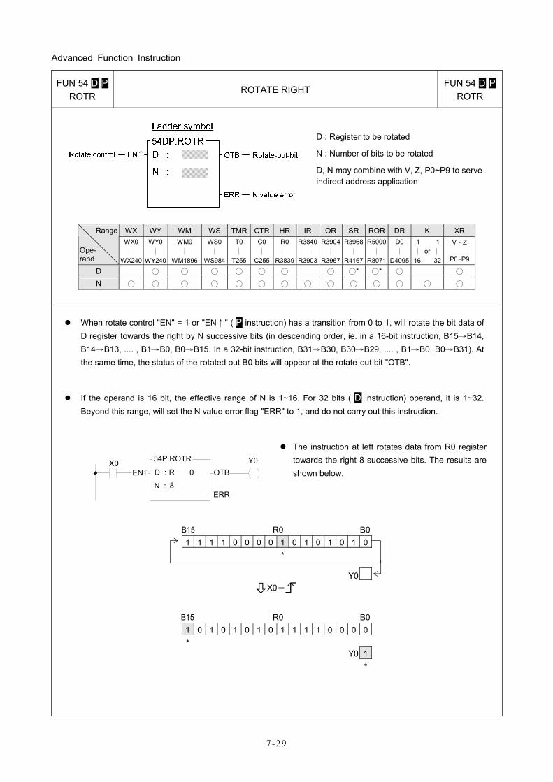
Advanced Function Instruction
7 -29
FUN 54 D P ROTR
ROTATE RIGHT FUN 54 D P
ROTR
D : Register to be rotated
N : Number of bits to be rotated
D, N may combine with V, Z, P0~P9 to serve indirect address application
WX WY WM WS TMR CTR HR IR OR SR ROR DR K XR Range
Ope- rand
WX0 ∣
WX240
WY0∣
WY240
WM0 ∣
WM1896
WS0 ∣
WS984
T0 ∣
T255
C0∣
C255
R0 ∣
R3839
R3840∣
R3903
R3904∣
R3967
R3968∣
R4167
R5000∣
R8071
D0 ∣
D4095
1 1 ∣ or ∣ 16 32
V、Z
P0~P9
D ○ ○ ○ ○ ○ ○ ○ ○* ○* ○ ○ N ○ ○ ○ ○ ○ ○ ○ ○ ○ ○ ○ ○ ○ ○
When rotate control "EN" = 1 or "EN↑" ( P instruction) has a transition from 0 to 1, will rotate the bit data of D register towards the right by N successive bits (in descending order, ie. in a 16-bit instruction, B15→B14, B14→B13, .... , B1→B0, B0→B15. In a 32-bit instruction, B31→B30, B30→B29, .... , B1→B0, B0→B31). At the same time, the status of the rotated out B0 bits will appear at the rotate-out bit "OTB".
If the operand is 16 bit, the effective range of N is 1~16. For 32 bits ( D instruction) operand, it is 1~32. Beyond this range, will set the N value error flag "ERR" to 1, and do not carry out this instruction.
X0EN D :
N :
R 0 OTBY0
ERR
54P.ROTR
8
The instruction at left rotates data from R0 register towards the right 8 successive bits. The results are shown below.
B15 R0 B0
1 1 1 1 0 0 0 0 1 0 1 0 1 0 1 0 *
Y0X0=
B15 R0 B0 1 0 1 0 1 0 1 0 1 1 1 1 0 0 0 0*
Y0 1 *
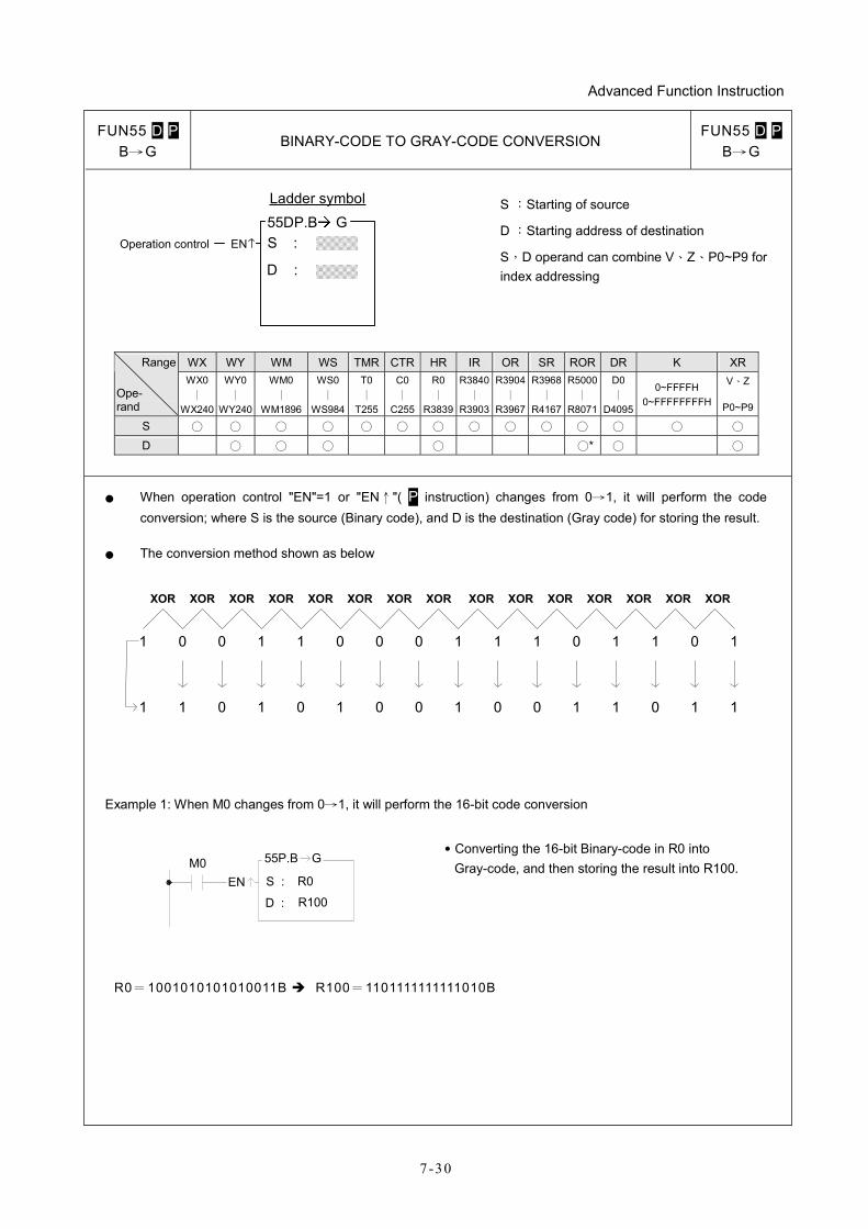
Advanced Function Instruction
7-30
FUN55 D P B→G
BINARY-CODE TO GRAY-CODE CONVERSION FUN55 D P
B→G
S :ENOperation control
Ladder symbol 55DP.B G
D :
S :Starting of source
D :Starting address of destination
S,D operand can combine V、Z、P0~P9 for index addressing
WX WY WM WS TMR CTR HR IR OR SR ROR DR K XRRange
Ope- rand
WX0 ∣
WX240
WY0 ∣
WY240
WM0 ∣
WM1896
WS0 ∣
WS984
T0 ∣
T255
C0∣
C255
R0∣
R3839
R3840∣
R3903
R3904∣
R3967
R3968∣
R4167
R5000∣
R8071
D0 ∣
D4095
0~FFFFH 0~FFFFFFFFH
V、Z
P0~P9
S ○ ○ ○ ○ ○ ○ ○ ○ ○ ○ ○ ○ ○ ○ D ○ ○ ○ ○ ○* ○ ○
● When operation control "EN"=1 or "EN↑"( P instruction) changes from 0→1, it will perform the code conversion; where S is the source (Binary code), and D is the destination (Gray code) for storing the result.
● The conversion method shown as below
1 100 1 00 0 1 1 1 0 1 1 0 1
XOR XOR XOR XOR XOR XOR XOR XOR XOR XOR XOR XOR XOR XOR XOR
1 101 0 01 0 1 0 0 1 1 0 1 1
Example 1: When M0 changes from 0→1, it will perform the 16-bit code conversion
EN S :
D :
M0 55P.B G
R0
R100
˙Converting the 16-bit Binary-code in R0 into Gray-code, and then storing the result into R100.
R0=1001010101010011B R100=1101111111111010B
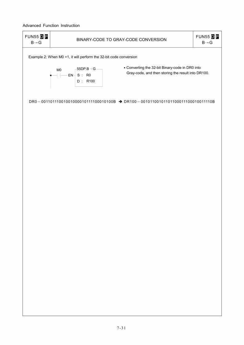
Advanced Function Instruction
7-31
FUN55 D P B→G
BINARY-CODE TO GRAY-CODE CONVERSION FUN55 D P
B→G
Example 2: When M0 =1, it will perform the 32-bit code conversion
S :
D : R100
R0M0
EN
55DP.B G
˙Converting the 32-bit Binary-code in DR0 into Gray-code, and then storing the result into DR100.
DR0=00110111001001000010111100010100B DR100=00101100101101100011100010011110B
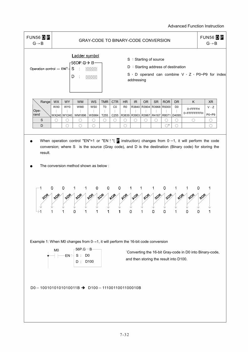
Advanced Function Instruction
7-32
FUN56 D P G→B
GRAY-CODE TO BINARY-CODE CONVERSION FUN56 D P
G→B
S :Starting of source
D :Starting address of destination
S , D operand can combine V 、 Z 、 P0~P9 for index addressing
WX WY WM WS TMR CTR HR IR OR SR ROR DR K XRRange
Ope- rand
WX0 ∣
WX240
WY0 ∣
WY240
WM0 ∣
WM1896
WS0 ∣
WS984
T0 ∣
T255
C0∣
C255
R0∣
R3839
R3840∣
R3903
R3904∣
R3967
R3968∣
R4167
R5000∣
R8071
D0 ∣
D4095
0~FFFFH 0~FFFFFFFFH
V、Z
P0~P9
S ○ ○ ○ ○ ○ ○ ○ ○ ○ ○ ○ ○ ○ ○ D ○ ○ ○ ○ ○* ○ ○
● When operation control "EN"=1 or "EN↑"( P instruction) changes from 0→1, it will perform the code conversion; where S is the source (Gray code), and D is the destination (Binary code) for storing the result.
● The conversion method shown as below :
Example 1: When M0 changes from 0→1, it will perform the 16-bit code conversion
M0EN S :
D : D100
D0
56P.G B
˙Converting the 16-bit Gray-code in D0 into Binary-code,
and then storing the result into D100.
D0=1001010101010011B D100=1110011001100010B
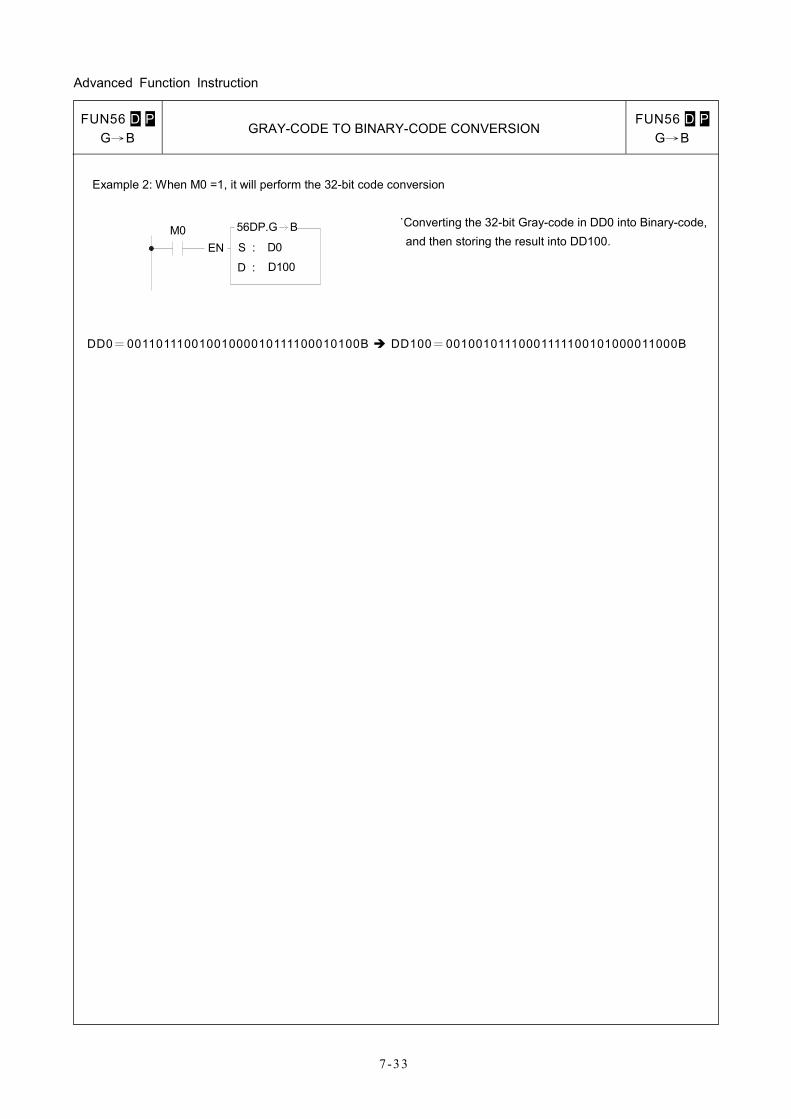
Advanced Function Instruction
7-33
FUN56 D P G→B
GRAY-CODE TO BINARY-CODE CONVERSION FUN56 D P
G→B
Example 2: When M0 =1, it will perform the 32-bit code conversion
S :
D :
M0EN D0
D100
56DP.G B
˙Converting the 32-bit Gray-code in DD0 into Binary-code, and then storing the result into DD100.
DD0=00110111001001000010111100010100B DD100=00100101110001111100101000011000B
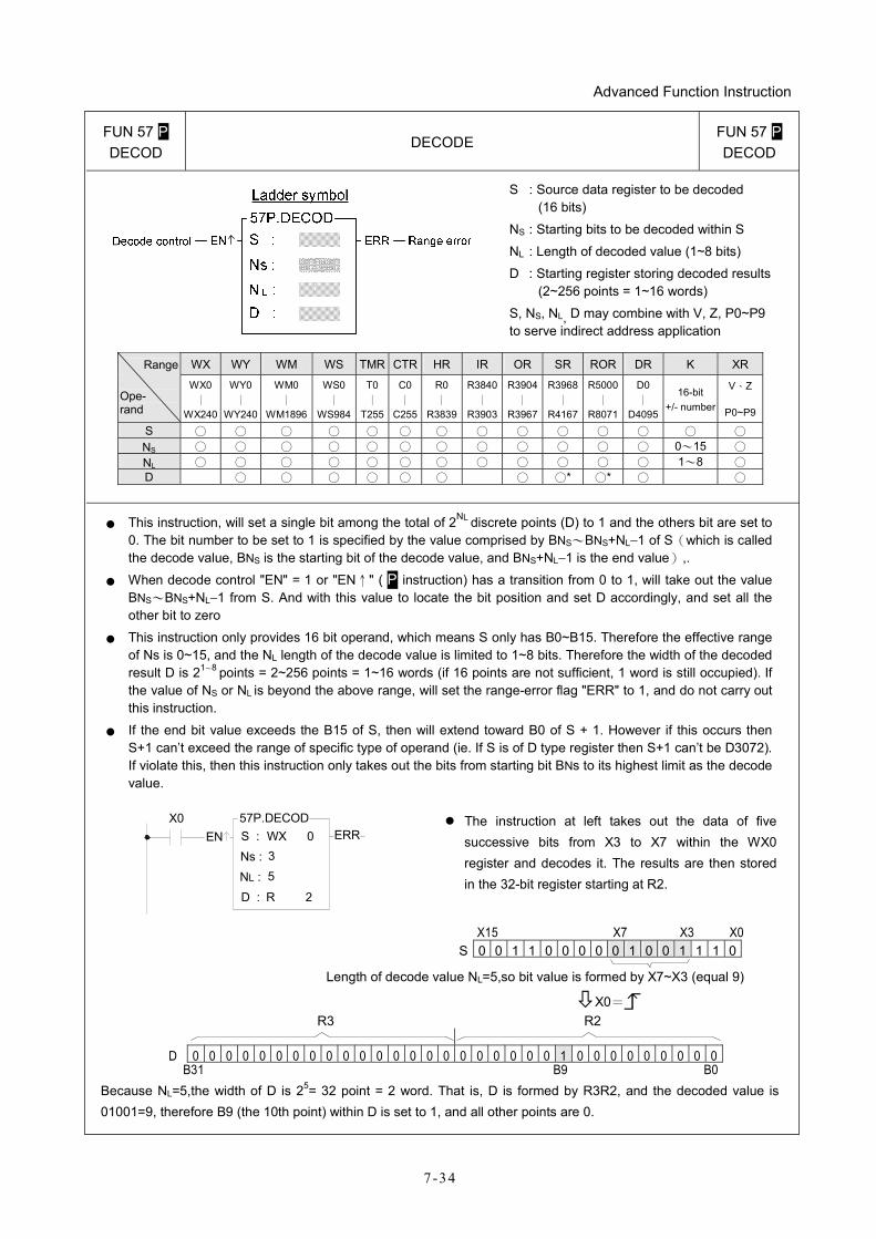
Advanced Function Instruction
7-34
FUN 57 P DECOD
DECODE FUN 57 P DECOD
S : Source data register to be decoded (16 bits)
NS : Starting bits to be decoded within S
NL : Length of decoded value (1~8 bits)
D : Starting register storing decoded results (2~256 points = 1~16 words)
S, NS, NL, D may combine with V, Z, P0~P9 to serve indirect address application
WX WY WM WS TMR CTR HR IR OR SR ROR DR K XR Range
Ope- rand
WX0 ∣
WX240
WY0 ∣
WY240
WM0 ∣
WM1896
WS0 ∣
WS984
T0∣
T255
C0∣
C255
R0 ∣
R3839
R3840∣
R3903
R3904∣
R3967
R3968∣
R4167
R5000∣
R8071
D0 ∣
D4095
16-bit +/- number
V、Z
P0~P9
S ○ ○ ○ ○ ○ ○ ○ ○ ○ ○ ○ ○ ○ ○ NS ○ ○ ○ ○ ○ ○ ○ ○ ○ ○ ○ ○ 0~15 ○ NL ○ ○ ○ ○ ○ ○ ○ ○ ○ ○ ○ ○ 1~8 ○ D ○ ○ ○ ○ ○ ○ ○ ○* ○* ○ ○
● This instruction, will set a single bit among the total of 2NL discrete points (D) to 1 and the others bit are set to
0. The bit number to be set to 1 is specified by the value comprised by BNS~BNS+NL−1 of S(which is called the decode value, BNS is the starting bit of the decode value, and BNS+NL−1 is the end value),.
● When decode control "EN" = 1 or "EN↑" ( P instruction) has a transition from 0 to 1, will take out the value BNS~BNS+NL−1 from S. And with this value to locate the bit position and set D accordingly, and set all the other bit to zero
● This instruction only provides 16 bit operand, which means S only has B0~B15. Therefore the effective range of Ns is 0~15, and the NL length of the decode value is limited to 1~8 bits. Therefore the width of the decoded result D is 21~8 points = 2~256 points = 1~16 words (if 16 points are not sufficient, 1 word is still occupied). If the value of NS or NL is beyond the above range, will set the range-error flag "ERR" to 1, and do not carry out this instruction.
● If the end bit value exceeds the B15 of S, then will extend toward B0 of S + 1. However if this occurs then S+1 can’t exceed the range of specific type of operand (ie. If S is of D type register then S+1 can’t be D3072). If violate this, then this instruction only takes out the bits from starting bit BNs to its highest limit as the decode value.
X0EN S :
Ns : 3
R 2
57P.DECODERR
D :
WX 0
NL : 5
The instruction at left takes out the data of five successive bits from X3 to X7 within the WX0 register and decodes it. The results are then stored in the 32-bit register starting at R2.
X15 X7 X3 X0 S 0 0 1 1 0 0 0 0 0 1 0 0 1 1 1 0
Length of decode value NL=5,so bit value is formed by X7~X3 (equal 9)
X0= R3 R2
D 0 0 0 0 0 0 0 0 0 0 0 0 0 0 0 0 0 0 0 0 0 0 1 0 0 0 0 0 0 0 0 0
B31 B9 B0 Because NL=5,the width of D is 25= 32 point = 2 word. That is, D is formed by R3R2, and the decoded value is 01001=9, therefore B9 (the 10th point) within D is set to 1, and all other points are 0.
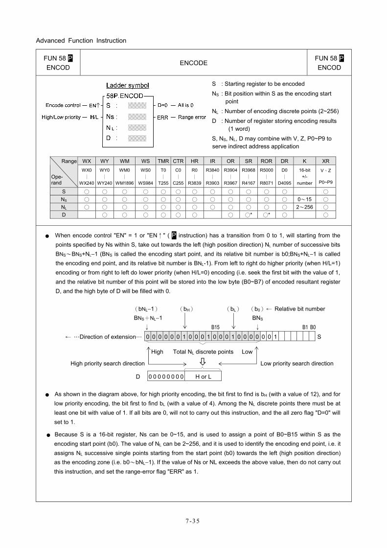
Advanced Function Instruction
7-35
FUN 58 P ENCOD
ENCODE FUN 58 P ENCOD
S : Starting register to be encoded
NS : Bit position within S as the encoding start point
NL : Number of encoding discrete points (2~256)
D : Number of register storing encoding results (1 word)
S, NS, NL, D may combine with V, Z, P0~P9 to serve indirect address application
WX WY WM WS TMR CTR HR IR OR SR ROR DR K XR Range
Ope- rand
WX0 ∣
WX240
WY0 ∣
WY240
WM0 ∣
WM1896
WS0 ∣
WS984
T0∣
T255
C0∣
C255
R0 ∣
R3839
R3840∣
R3903
R3904∣
R3967
R3968∣
R4167
R5000∣
R8071
D0 ∣
D4095
16-bit +/-
number
V、Z
P0~P9
S ○ ○ ○ ○ ○ ○ ○ ○ ○ ○ ○ ○ ○ NS ○ ○ ○ ○ ○ ○ ○ ○ ○ ○ ○ ○ 0~15 ○ NL ○ ○ ○ ○ ○ ○ ○ ○ ○ ○ ○ ○ 2~256 ○ D ○ ○ ○ ○ ○ ○ ○ ○* ○* ○ ○
● When encode control "EN" = 1 or "EN↑" ( P instruction) has a transition from 0 to 1, will starting from the points specified by Ns within S, take out towards the left (high position direction) NL number of successive bits BNS~BNS+NL−1 (BNS is called the encoding start point, and its relative bit number is b0;BNS+NL−1 is called the encoding end point, and its relative bit number is BNL-1). From left to right do higher priority (when H/L=1) encoding or from right to left do lower priority (when H/L=0) encoding (i.e. seek the first bit with the value of 1, and the relative bit number of this point will be stored into the low byte (B0~B7) of encoded resultant register D, and the high byte of D will be filled with 0.
(bNL−1) (bH) (bL) (b0)← Relative bit number BNS+NL−1 BNS ↓ B15 ↓ B1 B0
← …Direction of extension… 0 0 0 0 0 0 1 0 0 0 1 0 0 0 1 0 0 0 0 0 0 1 S
High Total NL discrete points Low
High priority search direction Low priority search direction
D 0 0 0 0 0 0 0 0 H or L
● As shown in the diagram above, for high priority encoding, the bit first to find is bH (with a value of 12), and for low priority encoding, the bit first to find bL (with a value of 4). Among the NL discrete points there must be at least one bit with value of 1. If all bits are 0, will not to carry out this instruction, and the all zero flag "D=0" will set to 1.
● Because S is a 16-bit register, Ns can be 0~15, and is used to assign a point of B0~B15 within S as the encoding start point (b0). The value of NL can be 2~256, and it is used to identify the encoding end point, i.e. it assigns NL successive single points starting from the start point (b0) towards the left (high position direction) as the encoding zone (i.e. b0~bNL−1). If the value of Ns or NL exceeds the above value, then do not carry out this instruction, and set the range-error flag "ERR" as 1.
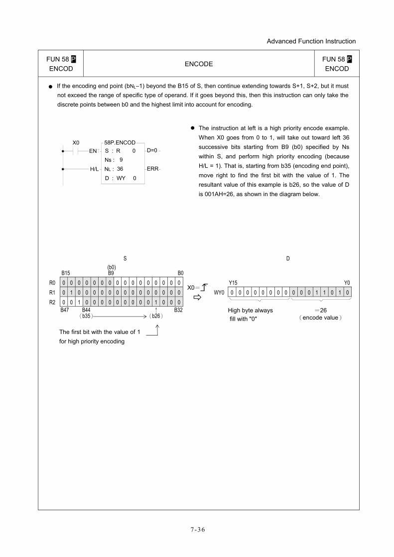
Advanced Function Instruction
7-36
FUN 58 P ENCOD
ENCODE FUN 58 P ENCOD
● If the encoding end point (bNL−1) beyond the B15 of S, then continue extending towards S+1, S+2, but it must not exceed the range of specific type of operand. If it goes beyond this, then this instruction can only take the discrete points between b0 and the highest limit into account for encoding.
X0EN S :
Ns : 9
WY 0
58P.ENCODD=0
D :
R 0
NL : 36H/L ERR
The instruction at left is a high priority encode example. When X0 goes from 0 to 1, will take out toward left 36 successive bits starting from B9 (b0) specified by Ns within S, and perform high priority encoding (because H/L = 1). That is, starting from b35 (encoding end point), move right to find the first bit with the value of 1. The resultant value of this example is b26, so the value of D is 001AH=26, as shown in the diagram below.
S D (b0) B15 B9 B0
R0 0 0 0 0 0 0 0 0 0 0 0 0 0 0 0 0 Y15 Y0R1 0 1 0 0 0 0 0 0 0 0 0 0 0 0 0 0 WY0 0 0 0 0 0 0 0 0 0 0 0 1 1 0 1 0R2 0 0 1 0 0 0 0 0 0 0 0 0 1 0 0 0
X0=
B47 B44
(b35) ↑ (b26)
B32 High byte always fill with "0"
=26 (encode value)
The first bit with the value of 1 for high priority encoding
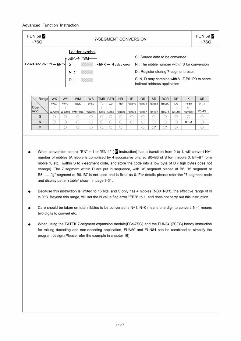
Advanced Function Instruction
7-37
FUN 59 P →7SG
7-SEGMENT CONVERSION FUN 59 P
→7SG
S : Source data to be converted
N : The nibble number within S for conversion
D : Register storing 7-segment result
S, N, D may combine with V, Z,P0~P9 to serve indirect address application
WX WY WM WS TMR CTR HR IR OR SR ROR DR K XR Range
Ope- rand
WX0 ∣
WX240
WY0 ∣
WY240
WM0 ∣
WM1896
WS0 ∣
WS984
T0∣
T255
C0∣
C255
R0 ∣
R3839
R3840∣
R3903
R3904∣
R3967
R3968∣
R4167
R5000∣
R8071
D0 ∣
D4095
16-bit +/-
number
V、Z
P0~P9
S ○ ○ ○ ○ ○ ○ ○ ○ ○ ○ ○ ○ ○ ○ N ○ ○ ○ ○ ○ ○ ○ ○ ○ ○ ○ ○ 0~3 ○ D ○ ○ ○ ○ ○ ○ ○ ○* ○* ○ ○
● When conversion control "EN" = 1 or "EN↑" ( P instruction) has a transition from 0 to 1, will convert N+1 number of nibbles (A nibble is comprised by 4 successive bits, so B0~B3 of S form nibble 0, B4~B7 form nibble 1, etc...)within S to 7-segment code, and store the code into a low byte of D (High bytes does not change). The 7 segment within D are put in sequence, with "a" segment placed at B6, "b" segment at B5, .... ,"g" segment at B0. B7 is not used and is fixed as 0. For details please refer the "7-segment code and display pattern table" shown in page 9-31.
● Because this instruction is limited to 16 bits, and S only has 4 nibbles (NB0~NB3), the effective range of N is 0~3. Beyond this range, will set the N value flag error "ERR" to 1, and does not carry out this instruction.
● Care should be taken on total nibbles to be converted is N+1. N=0 means one digit to convert, N=1 means two digits to convert etc…
● When using the FATEK 7-segment expansion module(FBs-7SG) and the FUN84 (7SEG) handy instruction for mixing decoding and non-decoding application, FUN59 and FUN84 can be combined to simplify the program design.(Please refer the example in chapter 16)
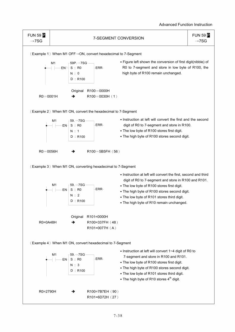
Advanced Function Instruction
7-38
FUN 59 P →7SG
7-SEGMENT CONVERSION FUN 59 P
→7SG
〈Example 1〉When M1 OFF→ON, convert hexadecimal to 7-Segment
M1EN S :
N : 0
R059P. 7SG
D : R100
ERR
˙Figure left shown the conversion of first digit(nibble) of R0 to 7-segment and store in low byte of R100, the high byte of R100 remain unchanged.
Original R100=0000H R0=0001H R100=0030H(1)
〈Example 2〉When M1 ON, convert the hexadecimal to 7-Segment
M1EN S :
N : 1
R059. 7SG
D : R100
ERR
˙Instruction at left will convert the first and the second digit of R0 to 7-segment and store in R100.
˙The low byte of R100 stores first digit. ˙The high byte of R100 stores second digit.
R0=0056H R100=5B5FH(56)
〈Example 3〉When M1 ON, converting hexadecimal to 7-Segment
M1EN S :
N :
R059. 7SG
D : R100
ERR
2
˙Instruction at left will convert the first, second and third digit of R0 to 7-segment and store in R100 and R101.
˙The low byte of R100 stores first digit. ˙The high byte of R100 stores second digit. ˙The low byte of R101 stores third digit. ˙The high byte of R10 remain unchanged.
Original R101=0000H R0=0A48H R100=337FH(48) R101=0077H(A)
〈Example 4〉When M1 ON, convert hexadecimal to 7-Segment
M1EN S :
N : 3
R059. 7SG
D : R100
ERR
˙Instruction at left will convert 1~4 digit of R0 to 7-segment and store in R100 and R101.
˙The low byte of R100 stores first digit. ˙The high byte of R100 stores second digit. ˙The low byte of R101 stores third digit. ˙The high byte of R10 stores 4th digit.
R0=2790H R100=7B7EH(90) R101=6D72H(27)
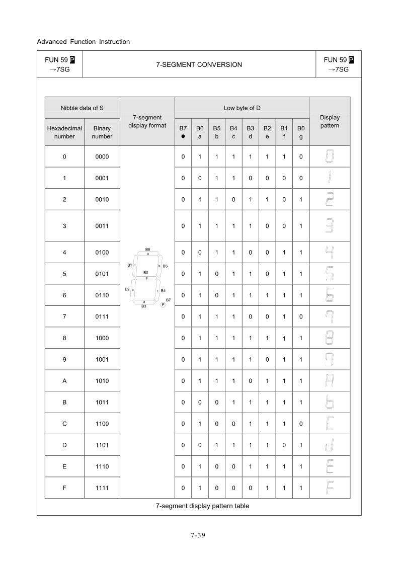
Advanced Function Instruction
7-39
FUN 59 P →7SG
7-SEGMENT CONVERSION FUN 59 P
→7SG
Nibble data of S Low byte of D
Hexadecimal number
Binary number
7-segment display format B7
B6a
B5b
B4c
B3d
B2e
B1 f
B0 g
Display pattern
0 0000 0 1 1 1 1 1 1 0
1 0001 0 0 1 1 0 0 0 0
2 0010 0 1 1 0 1 1 0 1
3 0011 0 1 1 1 1 0 0 1
4 0100 0 0 1 1 0 0 1 1
5 0101 0 1 0 1 1 0 1 1
6 0110 0 1 0 1 1 1 1 1
7 0111 0 1 1 1 0 0 1 0
8 1000 0 1 1 1 1 1 1 1
9 1001 0 1 1 1 1 0 1 1
A 1010 0 1 1 1 0 1 1 1
B 1011 0 0 0 1 1 1 1 1
C 1100 0 1 0 0 1 1 1 0
D 1101 0 0 1 1 1 1 0 1
E 1110 0 1 0 0 1 1 1 1
F 1111
B1
B2
B6
B5
B4
B0
B3B7
P
a
f
e c
g
b
d
0 1 0 0 0 1 1 1
7-segment display pattern table
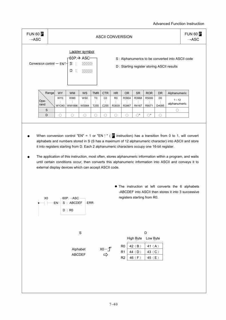
Advanced Function Instruction
7-40
FUN 60 P →ASC
ASCII CONVERSION FUN 60 P
→ASC
S : Alphanumerics to be converted into ASCII code
D : Starting register storing ASCII results
WY WM WS TMR CTR HR OR SR ROR DR Alphanumeric Range
Ope- rand
WY0 ∣
WY240
WM0 ∣
WM1896
WS0 ∣
WS984
T0 ∣
T255
C0 ∣
C255
R0 ∣
R3839
R3904∣
R3967
R3968∣
R4167
R5000∣
R8071
D0 ∣
D4095
1~12 alphanumeric
S ○ D ○ ○ ○ ○ ○ ○ ○ ○* ○* ○
● When conversion control "EN" = 1 or "EN↑" ( P instruction) has a transition from 0 to 1, will convert alphabets and numbers stored in S (S has a maximum of 12 alphanumeric character) into ASCII and store it into registers starting from D. Each 2 alphanumeric characters occupy one 16-bit register.
● The application of this instruction, most often, stores alphanumeric information within a program, and waits until certain conditions occur, then converts this alphanumeric information into ASCII and conveys it to external display devices which can accept ASCII code.
X0EN S : ABCDEF
60P. ASC
D :
ERR
R0
The instruction at left converts the 6 alphabets -ABCDEF into ASCII then stores it into 3 successive registers starting from R0.
S D High Byte Low Byte
R0 42(B) 41(A)
R1 44(D) 43(C) Alphabet ABCDEF
X0=
R2 46(F) 45(E)
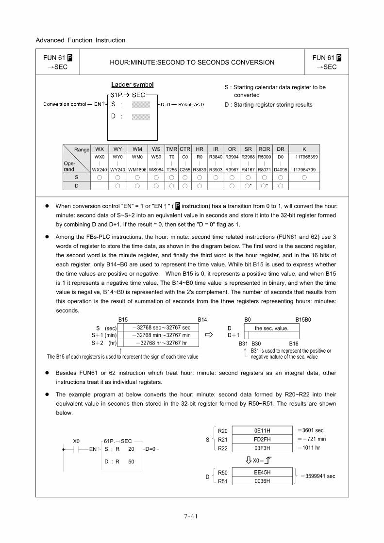
Advanced Function Instruction
7-41
FUN 61 P →SEC
HOUR:MINUTE:SECOND TO SECONDS CONVERSION FUN 61 P
→SEC
S : Starting calendar data register to be converted
D : Starting register storing results
WX WY WM WS TMR CTR HR IR OR SR ROR DR K Range
Ope- rand
WX0 ∣
WX240
WY0 ∣
WY240
WM0 ∣
WM1896
WS0∣
WS984
T0∣
T255
C0∣
C255
R0 ∣
R3839
R3840∣
R3903
R3904∣
R3967
R3968∣
R4167
R5000∣
R8071
D0 ∣
D4095
-117968399∣
117964799
S ○ ○ ○ ○ ○ ○ ○ ○ ○ ○ ○ ○ ○ D ○ ○ ○ ○ ○ ○ ○ ○* ○* ○
When conversion control "EN" = 1 or "EN↑" ( P instruction) has a transition from 0 to 1, will convert the hour: minute: second data of S~S+2 into an equivalent value in seconds and store it into the 32-bit register formed by combining D and D+1. If the result = 0, then set the "D = 0" flag as 1.
Among the FBs-PLC instructions, the hour: minute: second time related instructions (FUN61 and 62) use 3 words of register to store the time data, as shown in the diagram below. The first word is the second register, the second word is the minute register, and finally the third word is the hour register, and in the 16 bits of each register, only B14~B0 are used to represent the time value. While bit B15 is used to express whether the time values are positive or negative. When B15 is 0, it represents a positive time value, and when B15 is 1 it represents a negative time value. The B14~B0 time value is represented in binary, and when the time value is negative, B14~B0 is represented with the 2's complement. The number of seconds that results from this operation is the result of summation of seconds from the three registers representing hours: minutes: seconds.
B15 B14 B0 B15B0 S (sec) -32768 sec~32767 sec D the sec. value.
S+1 (min) -32768 min~32767 min D+1 S+2 (hr) -32768 hr~32767 hr B31 B30 B16
↑ ↑ B31 is used to represent the positive or The B15 of each registers is used to represent the sign of each time value └ negative nature of the sec. value
Besides FUN61 or 62 instruction which treat hour: minute: second registers as an integral data, other instructions treat it as individual registers.
The example program at below converts the hour: minute: second data formed by R20~R22 into their equivalent value in seconds then stored in the 32-bit register formed by R50~R51. The results are shown below.
R20 0E11H =3601 sec S R21 FD2FH =−721 min
R22 03F3H =1011 hr
X0=
R50 EE45H
X0EN S : R 20
61P. SEC
D : R 50
D=0
DR51 0036H
=3599941 sec
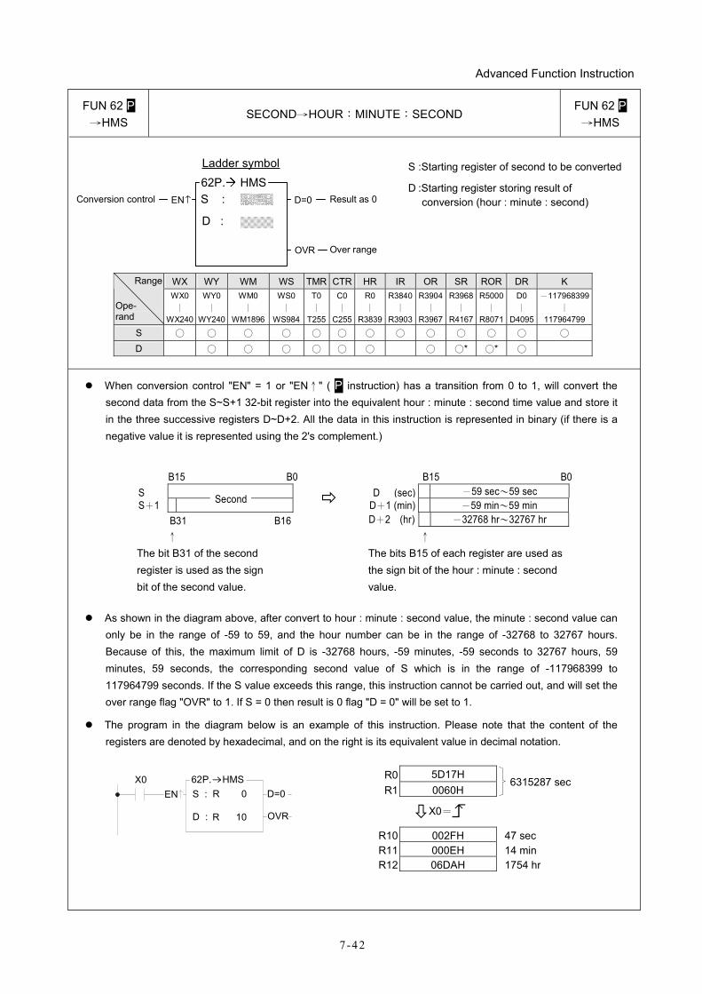
Advanced Function Instruction
7-42
FUN 62 P →HMS
SECOND→HOUR:MINUTE:SECOND FUN 62 P
→HMS
S :ENConversion control
Ladder symbol 62P. HMS
D :
D=0 Result as 0
OVR Over range
S :Starting register of second to be converted
D :Starting register storing result of conversion (hour : minute : second)
WX WY WM WS TMR CTR HR IR OR SR ROR DR K Range
Ope- rand
WX0 ∣
WX240
WY0 ∣
WY240
WM0 ∣
WM1896
WS0∣
WS984
T0∣
T255
C0∣
C255
R0 ∣
R3839
R3840∣
R3903
R3904∣
R3967
R3968∣
R4167
R5000 ∣
R8071
D0 ∣
D4095
-117968399∣
117964799
S ○ ○ ○ ○ ○ ○ ○ ○ ○ ○ ○ ○ ○ D ○ ○ ○ ○ ○ ○ ○ ○* ○* ○
When conversion control "EN" = 1 or "EN↑" ( P instruction) has a transition from 0 to 1, will convert the second data from the S~S+1 32-bit register into the equivalent hour : minute : second time value and store it in the three successive registers D~D+2. All the data in this instruction is represented in binary (if there is a negative value it is represented using the 2's complement.)
B15 B0 B15 B0 S D (sec) -59 sec~59 sec S+1
Second
D+1 (min) -59 min~59 min
B31 B16 D+2 (hr) -32768 hr~32767 hr ↑
The bit B31 of the second register is used as the sign bit of the second value.
↑ The bits B15 of each register are used as the sign bit of the hour : minute : second value.
As shown in the diagram above, after convert to hour : minute : second value, the minute : second value can only be in the range of -59 to 59, and the hour number can be in the range of -32768 to 32767 hours. Because of this, the maximum limit of D is -32768 hours, -59 minutes, -59 seconds to 32767 hours, 59 minutes, 59 seconds, the corresponding second value of S which is in the range of -117968399 to 117964799 seconds. If the S value exceeds this range, this instruction cannot be carried out, and will set the over range flag "OVR" to 1. If S = 0 then result is 0 flag "D = 0" will be set to 1.
The program in the diagram below is an example of this instruction. Please note that the content of the registers are denoted by hexadecimal, and on the right is its equivalent value in decimal notation.
R0 5D17H R1 0060H
6315287 sec
X0=
R10 002FH 47 sec R11 000EH 14 min
X0EN S : R 0
62P. HMS
D : R 10
D=0
OVR
R12 06DAH 1754 hr
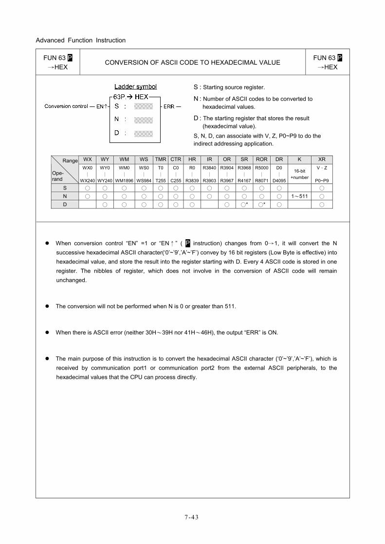
Advanced Function Instruction
7-43
FUN 63 P →HEX
CONVERSION OF ASCII CODE TO HEXADECIMAL VALUE FUN 63 P
→HEX
S : Starting source register.
N : Number of ASCII codes to be converted to hexadecimal values.
D : The starting register that stores the result (hexadecimal value).
S, N, D, can associate with V, Z, P0~P9 to do the indirect addressing application.
WX WY WM WS TMR CTR HR IR OR SR ROR DR K XR Range
Ope- rand
WX0 ∣
WX240
WY0 ∣
WY240
WM0 ∣
WM1896
WS0 ∣
WS984
T0∣
T255
C0∣
C255
R0 ∣
R3839
R3840∣
R3903
R3904∣
R3967
R3968∣
R4167
R5000∣
R8071
D0 ∣
D4095
16-bit +number
V、Z
P0~P9
S ○ ○ ○ ○ ○ ○ ○ ○ ○ ○ ○ ○ ○ N ○ ○ ○ ○ ○ ○ ○ ○ ○ ○ ○ ○ 1~511 ○ D ○ ○ ○ ○ ○ ○ ○ ○* ○* ○ ○
When conversion control “EN” =1 or “EN↑” ( P instruction) changes from 0→1, it will convert the N successive hexadecimal ASCII character(‘0’~’9’,’A’~’F’) convey by 16 bit registers (Low Byte is effective) into hexadecimal value, and store the result into the register starting with D. Every 4 ASCII code is stored in one register. The nibbles of register, which does not involve in the conversion of ASCII code will remain unchanged.
The conversion will not be performed when N is 0 or greater than 511.
When there is ASCII error (neither 30H~39H nor 41H~46H), the output “ERR” is ON.
The main purpose of this instruction is to convert the hexadecimal ASCII character (‘0’~’9’,’A’~’F’), which is received by communication port1 or communication port2 from the external ASCII peripherals, to the hexadecimal values that the CPU can process directly.
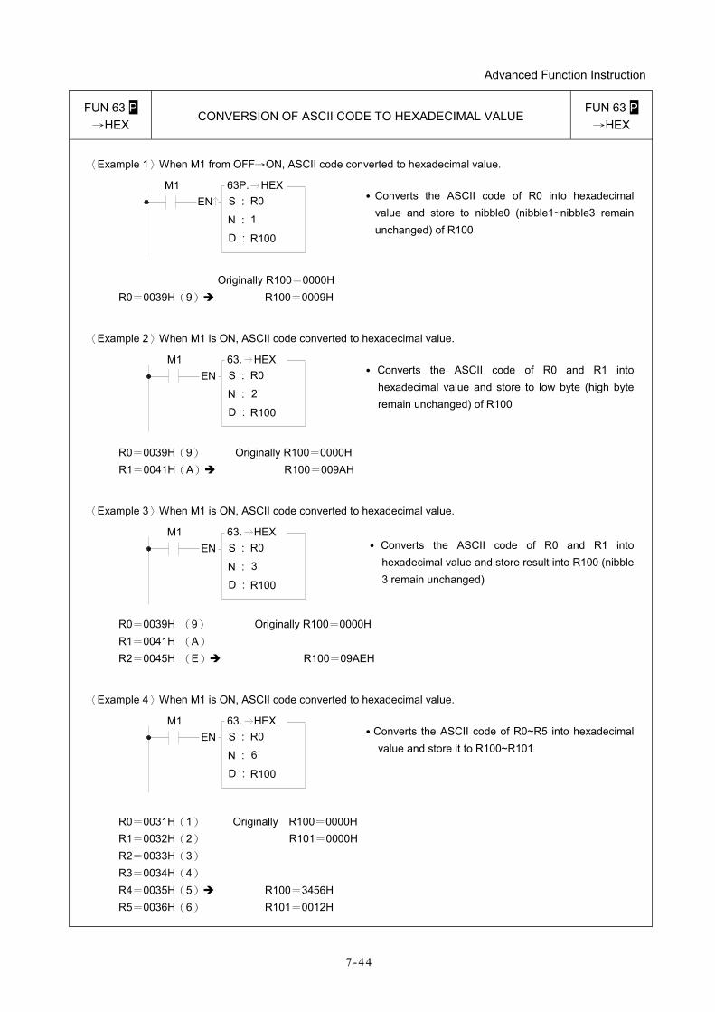
Advanced Function Instruction
7-44
FUN 63 P →HEX
CONVERSION OF ASCII CODE TO HEXADECIMAL VALUE FUN 63 P
→HEX
〈Example 1〉When M1 from OFF→ON, ASCII code converted to hexadecimal value.
M1EN S :
N : 1
R063P. HEX
D : R100
˙Converts the ASCII code of R0 into hexadecimal value and store to nibble0 (nibble1~nibble3 remain unchanged) of R100
Originally R100=0000H R0=0039H(9) R100=0009H
〈Example 2〉When M1 is ON, ASCII code converted to hexadecimal value.
M1EN S :
N : 2
R063. HEX
D : R100
˙ Converts the ASCII code of R0 and R1 into hexadecimal value and store to low byte (high byte remain unchanged) of R100
R0=0039H(9) Originally R100=0000H R1=0041H(A) R100=009AH
〈Example 3〉When M1 is ON, ASCII code converted to hexadecimal value.
M1EN S :
N :
R063. HEX
D : R100
3
˙ Converts the ASCII code of R0 and R1 into
hexadecimal value and store result into R100 (nibble 3 remain unchanged)
R0=0039H (9) Originally R100=0000H R1=0041H (A) R2=0045H (E) R100=09AEH
〈Example 4〉When M1 is ON, ASCII code converted to hexadecimal value.
M1EN S :
N :
R063. HEX
D : R100
6
˙Converts the ASCII code of R0~R5 into hexadecimal value and store it to R100~R101
R0=0031H(1) Originally R100=0000H R1=0032H(2) R101=0000H R2=0033H(3) R3=0034H(4) R4=0035H(5) R100=3456H R5=0036H(6) R101=0012H
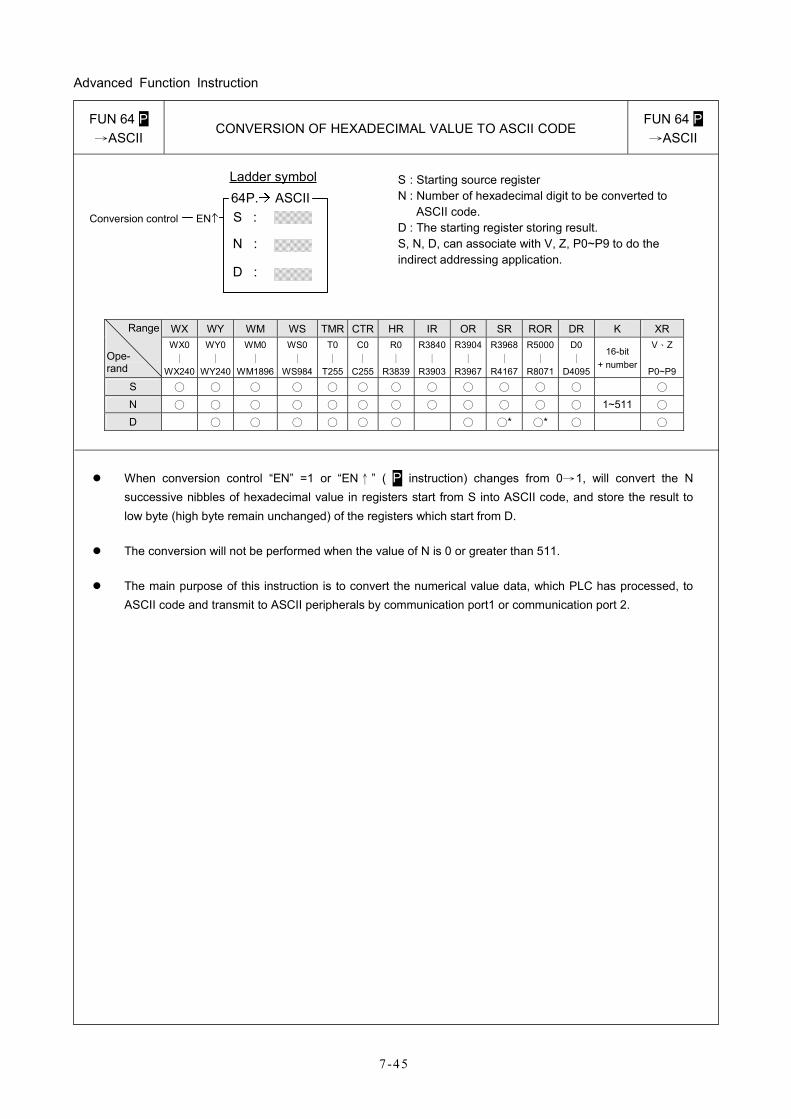
Advanced Function Instruction
7-45
FUN 64 P →ASCII
CONVERSION OF HEXADECIMAL VALUE TO ASCII CODE FUN 64 P →ASCII
S :ENConversion control
Ladder symbol 64P. ASCII
N :
D :
S : Starting source register N : Number of hexadecimal digit to be converted to
ASCII code. D : The starting register storing result. S, N, D, can associate with V, Z, P0~P9 to do the indirect addressing application.
WX WY WM WS TMR CTR HR IR OR SR ROR DR K XR Range
Ope- rand
WX0 ∣
WX240
WY0 ∣
WY240
WM0 ∣
WM1896
WS0 ∣
WS984
T0∣
T255
C0∣
C255
R0 ∣
R3839
R3840∣
R3903
R3904∣
R3967
R3968∣
R4167
R5000∣
R8071
D0 ∣
D4095
16-bit + number
V、Z
P0~P9
S ○ ○ ○ ○ ○ ○ ○ ○ ○ ○ ○ ○ ○ N ○ ○ ○ ○ ○ ○ ○ ○ ○ ○ ○ ○ 1~511 ○ D ○ ○ ○ ○ ○ ○ ○ ○* ○* ○ ○
When conversion control “EN” =1 or “EN↑” ( P instruction) changes from 0→1, will convert the N successive nibbles of hexadecimal value in registers start from S into ASCII code, and store the result to low byte (high byte remain unchanged) of the registers which start from D.
The conversion will not be performed when the value of N is 0 or greater than 511.
The main purpose of this instruction is to convert the numerical value data, which PLC has processed, to ASCII code and transmit to ASCII peripherals by communication port1 or communication port 2.
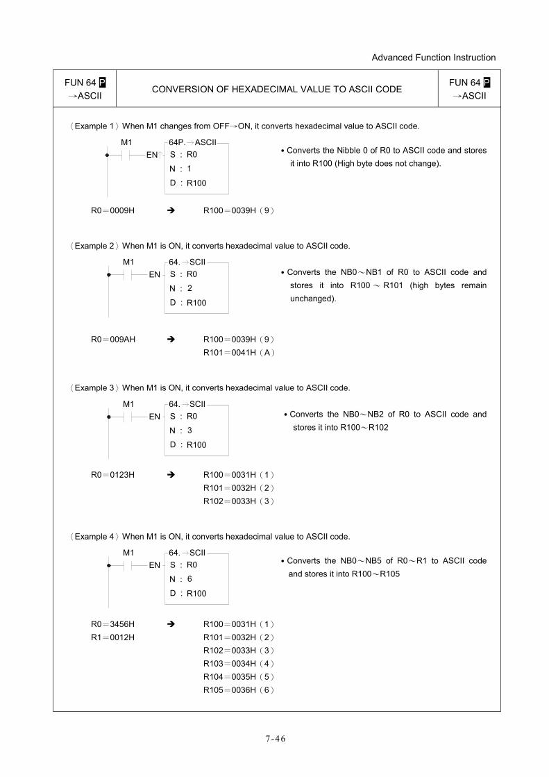
Advanced Function Instruction
7-46
FUN 64 P →ASCII
CONVERSION OF HEXADECIMAL VALUE TO ASCII CODE FUN 64 P →ASCII
〈Example 1〉When M1 changes from OFF→ON, it converts hexadecimal value to ASCII code.
M1EN S :
N : 1
R064P. ASCII
D : R100
˙Converts the Nibble 0 of R0 to ASCII code and stores it into R100 (High byte does not change).
R0=0009H R100=0039H(9)
〈Example 2〉When M1 is ON, it converts hexadecimal value to ASCII code.
M1EN S :
N : 2
R0
D : R100
64. SCII
˙Converts the NB0~NB1 of R0 to ASCII code and
stores it into R100 ~ R101 (high bytes remain unchanged).
R0=009AH R100=0039H(9) R101=0041H(A)
〈Example 3〉When M1 is ON, it converts hexadecimal value to ASCII code.
M1EN S :
N :
R064. SCII
D : R100
3
˙Converts the NB0~NB2 of R0 to ASCII code and
stores it into R100~R102
R0=0123H R100=0031H(1) R101=0032H(2) R102=0033H(3)
〈Example 4〉When M1 is ON, it converts hexadecimal value to ASCII code.
M1EN S :
N :
R064. SCII
D : R100
6
˙Converts the NB0~NB5 of R0~R1 to ASCII code and stores it into R100~R105
R0=3456H R100=0031H(1) R1=0012H R101=0032H(2)
R102=0033H(3) R103=0034H(4) R104=0035H(5) R105=0036H(6)
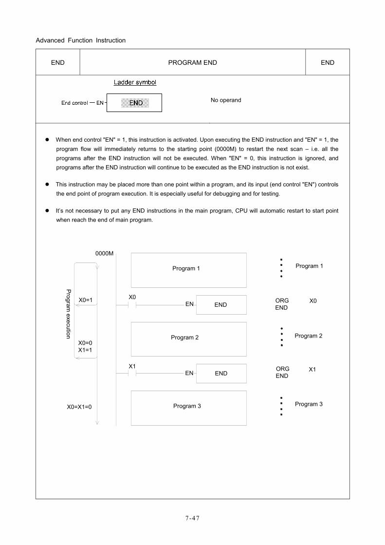
Advanced Function Instruction
7-47
END PROGRAM END END
No operand
When end control "EN" = 1, this instruction is activated. Upon executing the END instruction and "EN" = 1, the program flow will immediately returns to the starting point (0000M) to restart the next scan – i.e. all the programs after the END instruction will not be executed. When "EN" = 0, this instruction is ignored, and programs after the END instruction will continue to be executed as the END instruction is not exist.
This instruction may be placed more than one point within a program, and its input (end control "EN") controls the end point of program execution. It is especially useful for debugging and for testing.
It’s not necessary to put any END instructions in the main program, CPU will automatic restart to start point when reach the end of main program.
Program 1
X0
Program 2
Program 3
X1
X0=X1=0
Program 1
Program 2
END
0000M
X0=1
X0=0X1=1
X0
X1END
Program 3
EN
EN
Program
execution
ORGEND
ORGEND
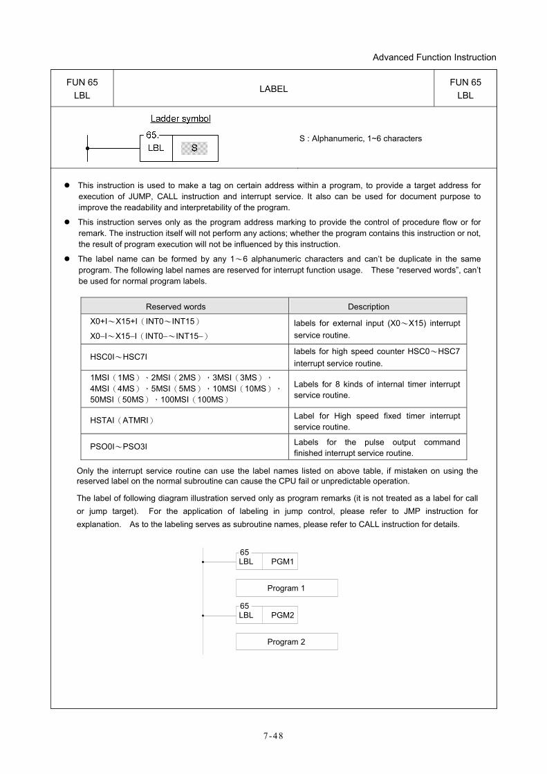
Advanced Function Instruction
7 -48
FUN 65 LBL
LABEL FUN 65
LBL
S : Alphanumeric, 1~6 characters
This instruction is used to make a tag on certain address within a program, to provide a target address for execution of JUMP, CALL instruction and interrupt service. It also can be used for document purpose to improve the readability and interpretability of the program.
This instruction serves only as the program address marking to provide the control of procedure flow or for remark. The instruction itself will not perform any actions; whether the program contains this instruction or not, the result of program execution will not be influenced by this instruction.
The label name can be formed by any 1~6 alphanumeric characters and can’t be duplicate in the same program. The following label names are reserved for interrupt function usage. These “reserved words”, can’t be used for normal program labels.
Reserved words Description
X0+I~X15+I(INT0~INT15)
X0−I~X15−I(INT0−~INT15−) labels for external input (X0~X15) interrupt service routine.
HSC0I~HSC7I labels for high speed counter HSC0~HSC7 interrupt service routine.
1MSI(1MS)、2MSI(2MS),3MSI(3MS), 4MSI(4MS),5MSI(5MS),10MSI(10MS),
50MSI(50MS),100MSI(100MS)
Labels for 8 kinds of internal timer interrupt service routine.
HSTAI(ATMRI) Label for High speed fixed timer interrupt service routine.
PSO0I~PSO3I Labels for the pulse output command finished interrupt service routine.
Only the interrupt service routine can use the label names listed on above table, if mistaken on using the reserved label on the normal subroutine can cause the CPU fail or unpredictable operation.
The label of following diagram illustration served only as program remarks (it is not treated as a label for call or jump target). For the application of labeling in jump control, please refer to JMP instruction for explanation. As to the labeling serves as subroutine names, please refer to CALL instruction for details.
65LBL PGM1
Program 1
65LBL PGM2
Program 2
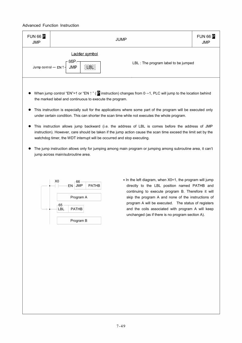
Advanced Function Instruction
7-49
FUN 66 P JMP
JUMP FUN 66 P
JMP
LBL : The program label to be jumped
When jump control “EN”=1 or “EN↑” ( P instruction) changes from 0→1, PLC will jump to the location behind the marked label and continuous to execute the program.
This instruction is especially suit for the applications where some part of the program will be executed only under certain condition. This can shorter the scan time while not executes the whole program.
This instruction allows jump backward (i.e. the address of LBL is comes before the address of JMP instruction). However, care should be taken if the jump action cause the scan time exceed the limit set by the watchdog timer, the WDT interrupt will be occurred and stop executing.
The jump instruction allows only for jumping among main program or jumping among subroutine area, it can’t jump across main/subroutine area.
66JMP PATHB
Program A
65LBL
Program B
X0EN
PATHB
˙In the left diagram, when X0=1, the program will jump directly to the LBL position named PATHB and continuing to execute program B. Therefore it will skip the program A and none of the instructions of program A will be executed. The status of registers and the coils associated with program A will keep unchanged (as if there is no program section A).
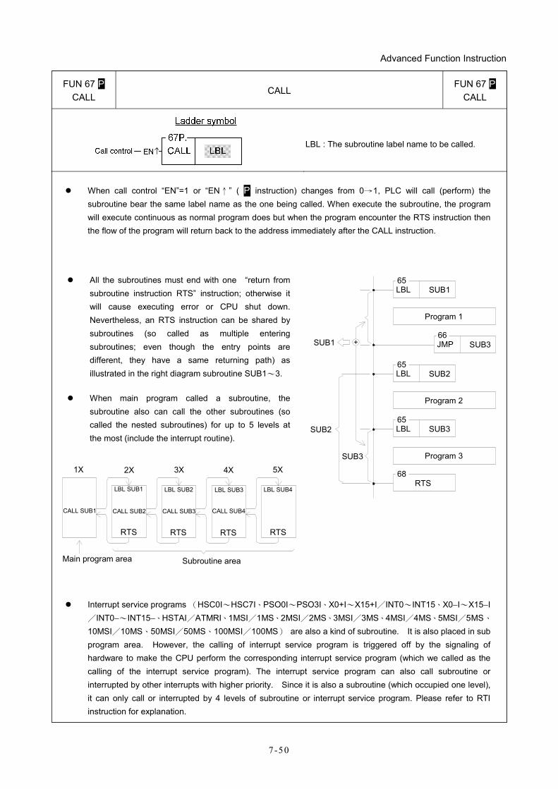
Advanced Function Instruction
7 -50
FUN 67 P CALL
CALL FUN 67 P
CALL
LBL : The subroutine label name to be called.
When call control “EN”=1 or “EN↑” ( P instruction) changes from 0→1, PLC will call (perform) the subroutine bear the same label name as the one being called. When execute the subroutine, the program will execute continuous as normal program does but when the program encounter the RTS instruction then the flow of the program will return back to the address immediately after the CALL instruction.
All the subroutines must end with one “return from subroutine instruction RTS” instruction; otherwise it will cause executing error or CPU shut down. Nevertheless, an RTS instruction can be shared by subroutines (so called as multiple entering subroutines; even though the entry points are different, they have a same returning path) as illustrated in the right diagram subroutine SUB1~3.
When main program called a subroutine, the subroutine also can call the other subroutines (so called the nested subroutines) for up to 5 levels at the most (include the interrupt routine).
1X 2X 3X 4X 5X
RTS RTS RTS RTS
Main program area Subroutine area
CALL SUB1
LBL SUB1
CALL SUB2 CALL SUB3 CALL SUB4
LBL SUB2 LBL SUB3 LBL SUB4
65LBL SUB1
Program 1
65LBL SUB2
Program 2
66JMP SUB3
65LBL SUB3
Program 3
68RTS
SUB3
SUB2
+SUB1
Interrupt service programs (HSC0I~HSC7I、PSO0I~PSO3I、X0+I~X15+I/INT0~INT15、X0−I~X15−I/INT0−~INT15−、HSTAI/ATMRI、1MSI/1MS、2MSI/2MS、3MSI/3MS、4MSI/4MS、5MSI/5MS、10MSI/10MS、50MSI/50MS、100MSI/100MS) are also a kind of subroutine. It is also placed in sub program area. However, the calling of interrupt service program is triggered off by the signaling of hardware to make the CPU perform the corresponding interrupt service program (which we called as the calling of the interrupt service program). The interrupt service program can also call subroutine or interrupted by other interrupts with higher priority. Since it is also a subroutine (which occupied one level), it can only call or interrupted by 4 levels of subroutine or interrupt service program. Please refer to RTI instruction for explanation.
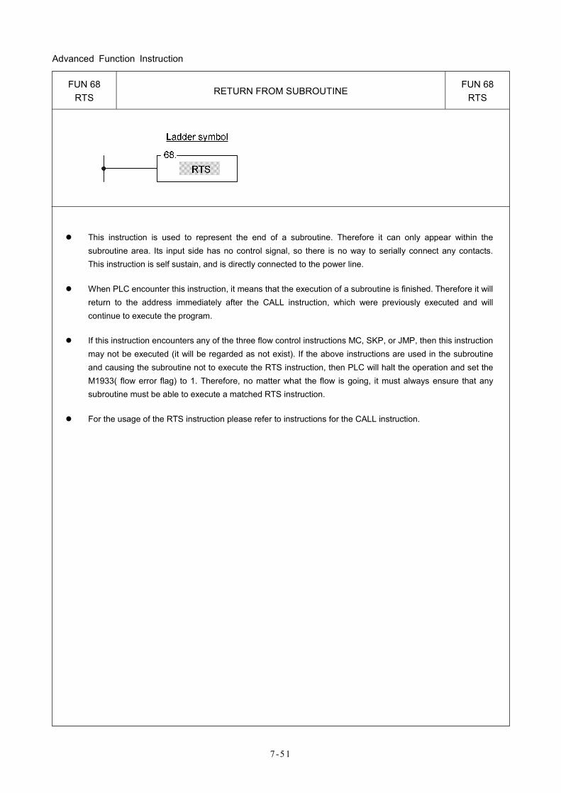
Advanced Function Instruction
7-51
FUN 68 RTS
RETURN FROM SUBROUTINE FUN 68
RTS
This instruction is used to represent the end of a subroutine. Therefore it can only appear within the subroutine area. Its input side has no control signal, so there is no way to serially connect any contacts. This instruction is self sustain, and is directly connected to the power line.
When PLC encounter this instruction, it means that the execution of a subroutine is finished. Therefore it will return to the address immediately after the CALL instruction, which were previously executed and will continue to execute the program.
If this instruction encounters any of the three flow control instructions MC, SKP, or JMP, then this instruction may not be executed (it will be regarded as not exist). If the above instructions are used in the subroutine and causing the subroutine not to execute the RTS instruction, then PLC will halt the operation and set the M1933( flow error flag) to 1. Therefore, no matter what the flow is going, it must always ensure that any subroutine must be able to execute a matched RTS instruction.
For the usage of the RTS instruction please refer to instructions for the CALL instruction.
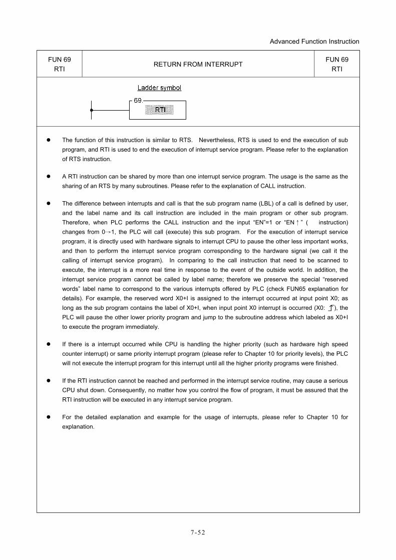
Advanced Function Instruction
7 -52
FUN 69 RTI
RETURN FROM INTERRUPT FUN 69
RTI
The function of this instruction is similar to RTS. Nevertheless, RTS is used to end the execution of sub program, and RTI is used to end the execution of interrupt service program. Please refer to the explanation of RTS instruction.
A RTI instruction can be shared by more than one interrupt service program. The usage is the same as the sharing of an RTS by many subroutines. Please refer to the explanation of CALL instruction.
The difference between interrupts and call is that the sub program name (LBL) of a call is defined by user, and the label name and its call instruction are included in the main program or other sub program. Therefore, when PLC performs the CALL instruction and the input “EN”=1 or “EN↑” ( instruction) changes from 0→1, the PLC will call (execute) this sub program. For the execution of interrupt service program, it is directly used with hardware signals to interrupt CPU to pause the other less important works, and then to perform the interrupt service program corresponding to the hardware signal (we call it the calling of interrupt service program). In comparing to the call instruction that need to be scanned to execute, the interrupt is a more real time in response to the event of the outside world. In addition, the interrupt service program cannot be called by label name; therefore we preserve the special “reserved words” label name to correspond to the various interrupts offered by PLC (check FUN65 explanation for details). For example, the reserved word X0+I is assigned to the interrupt occurred at input point X0; as long as the sub program contains the label of X0+I, when input point X0 interrupt is occurred (X0: ), the PLC will pause the other lower priority program and jump to the subroutine address which labeled as X0+I to execute the program immediately.
If there is a interrupt occurred while CPU is handling the higher priority (such as hardware high speed counter interrupt) or same priority interrupt program (please refer to Chapter 10 for priority levels), the PLC will not execute the interrupt program for this interrupt until all the higher priority programs were finished.
If the RTI instruction cannot be reached and performed in the interrupt service routine, may cause a serious CPU shut down. Consequently, no matter how you control the flow of program, it must be assured that the RTI instruction will be executed in any interrupt service program.
For the detailed explanation and example for the usage of interrupts, please refer to Chapter 10 for explanation.
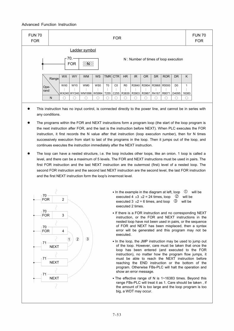
Advanced Function Instruction
7-53
FUN 70 FOR
FOR FUN 70
FOR
FOR
Ladder symbol
70.N
N : Number of times of loop execution
WX WY WM WS TMR CTR HR IR OR SR ROR DR K
Range
Ope- rand
WX0 ∣
WX240
WY0 ∣
WY240
WM0 ∣
WM1896
WS0∣
WS984
T0∣
T255
C0∣
C255
R0 ∣
R3839
R3840∣
R3903
R3904∣
R3967
R3968∣
R4167
R5000 ∣
R8071
D0 ∣
D4095
1 ∣
16383
N ○ ○ ○ ○ ○ ○ ○ ○ ○ ○ ○ ○ ○
This instruction has no input control, is connected directly to the power line, and cannot be in series with any conditions.
The programs within the FOR and NEXT instructions form a program loop (the start of the loop program is the next instruction after FOR, and the last is the instruction before NEXT). When PLC executes the FOR instruction, it first records the N value after that instruction (loop execution number), then for N times successively execution from start to last of the programs in the loop. Then it jumps out of the loop, and continues executes the instruction immediately after the NEXT instruction.
The loop can have a nested structure, i.e. the loop includes other loops, like an onion. 1 loop is called a level, and there can be a maximum of 5 levels. The FOR and NEXT instructions must be used in pairs. The first FOR instruction and the last NEXT instruction are the outermost (first) level of a nested loop. The second FOR instruction and the second last NEXT instruction are the second level, the last FOR instruction and the first NEXT instruction form the loop's innermost level.
71NEXT
FOR 4
FOR 3
70FOR 2
NEXT
NEXT
70
70
71
71
2 31
˙In the example in the diagram at left, loop will be executed 4 ×3 ×2 = 24 times, loop will be executed 3 ×2 = 6 times, and loop will be executed 2 times.
˙If there is a FOR instruction and no corresponding NEXT instruction, or the FOR and NEXT instructions in the nested loop have not been used in pairs, or the sequence of FOR and NEXT has been misplaced, then a syntax error will be generated and this program may not be executed.
˙In the loop, the JMP instruction may be used to jump out of the loop. However, care must be taken that once the loop has been entered (and executed to the FOR instruction), no matter how the program flow jumps, it must be able to reach the NEXT instruction before reaching the END instruction or the bottom of the program. Otherwise FBs-PLC will halt the operation and show an error message.
˙The effective range of N is 1~16383 times. Beyond this range FBs-PLC will treat it as 1. Care should be taken , if the amount of N is too large and the loop program is too big, a WDT may occur.
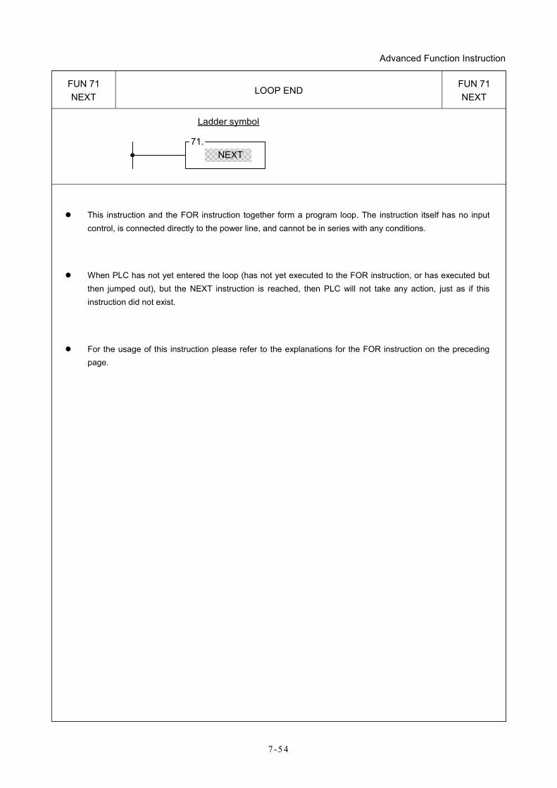
Advanced Function Instruction
7 -54
FUN 71 NEXT
LOOP END FUN 71 NEXT
Ladder symbol
71.NEXT
This instruction and the FOR instruction together form a program loop. The instruction itself has no input control, is connected directly to the power line, and cannot be in series with any conditions.
When PLC has not yet entered the loop (has not yet executed to the FOR instruction, or has executed but then jumped out), but the NEXT instruction is reached, then PLC will not take any action, just as if this instruction did not exist.
For the usage of this instruction please refer to the explanations for the FOR instruction on the preceding page.
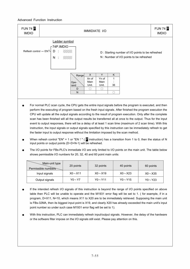
Advanced Function Instruction
7-55
FUN 74 P IMDIO
IMMIDIATE I/O FUN 74 P
IMDIO
D :ENReflesh control
Ladder symbol 74P.IMDIO
N :
D : Starting number of I/O points to be refreshed N : Number of I/O points to be refreshed
X Y K Range
Ope- rand
Xn of Main Unit.
Yn of Main Unit.
1 ∣ 36
D ○ ○ N ○
● For normal PLC scan cycle, the CPU gets the entire input signals before the program is executed, and then perform the executing of program based on the fresh input signals. After finished the program execution the CPU will update all the output signals according to the result of program execution. Only after the complete scan has been finished will all the output results be transferred all at once to the output. Thus for the input event to output responses, there will be a delay of at least 1 scan time (maximum of 2 scan time). With this instruction, the input signals or output signals specified by this instruction can be immediately refresh to get the faster input to output response without the limitation imposed by the scan method.
● When refresh control "EN" = 1 or "EN↑" ( P instruction) has a transition from 1 to 0, then the status of N input points or output points (D~D+N-1) will be refreshed.
● The I/O points for FBs-PLC's immediate I/O are only limited to I/O points on the main unit. The table below shows permissible I/O numbers for 20, 32, 40 and 60 point main units:
Main-unit type
Permissible numbers 20 points 32 points 40 points 60 points
Input signals X0~X11 X0~X19 X0~X23 X0~X35
Output signals Y0~Y7 Y0~Y11 Y0~Y15 Y0~Y23
● If the intended refresh I/O signals of this instruction is beyond the range of I/O points specified on above table then PLC will be unable to operate and the M1931 error flag will be set to 1. ( for example, if in a program, D=X11, N=10, which means X11 to X20 are to be immediately retrieved. Supposing the main unit is FBs-32MA, then its biggest input point is X19, and clearly X20 has already exceeded the main unit's input point number so under such case M1931 error flag will be set to 1).
● With this instruction, PLC can immediately refresh input/output signals. However, the delay of the hardware or the software filter impose on the I/O signals still exist. Please pay attention on this.
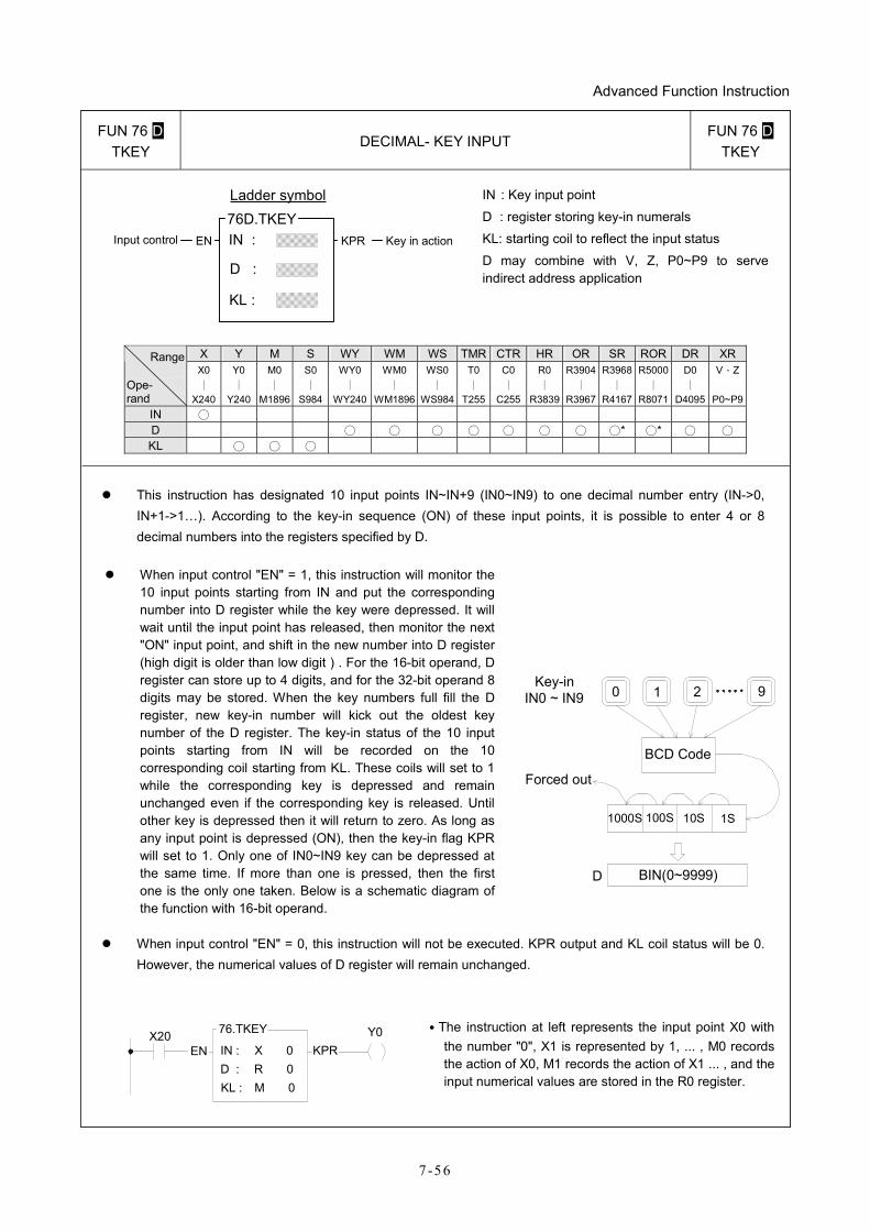
Advanced Function Instruction
7 -56
FUN 76 D TKEY
DECIMAL- KEY INPUT FUN 76 D
TKEY
IN :ENInput control
Ladder symbol 76D.TKEY
D :
KPR
KL :
Key in action
IN : Key input point
D : register storing key-in numerals
KL: starting coil to reflect the input status
D may combine with V, Z, P0~P9 to serve indirect address application
X Y M S WY WM WS TMR CTR HR OR SR ROR DR XRRange
Ope- rand
X0 ∣
X240
Y0 ∣
Y240
M0 ∣
M1896
S0 ∣
S984
WY0∣
WY240
WM0∣
WM1896
WS0∣
WS984
T0∣
T255
C0 ∣
C255
R0 ∣
R3839
R3904∣
R3967
R3968 ∣
R4167
R5000 ∣
R8071
D0 ∣
D4095
V、Z
P0~P9IN ○ D ○ ○ ○ ○ ○ ○ ○ ○* ○* ○ ○
KL ○ ○ ○
This instruction has designated 10 input points IN~IN+9 (IN0~IN9) to one decimal number entry (IN->0, IN+1->1…). According to the key-in sequence (ON) of these input points, it is possible to enter 4 or 8 decimal numbers into the registers specified by D.
When input control "EN" = 1, this instruction will monitor the 10 input points starting from IN and put the corresponding number into D register while the key were depressed. It will wait until the input point has released, then monitor the next "ON" input point, and shift in the new number into D register (high digit is older than low digit ) . For the 16-bit operand, D register can store up to 4 digits, and for the 32-bit operand 8 digits may be stored. When the key numbers full fill the D register, new key-in number will kick out the oldest key number of the D register. The key-in status of the 10 input points starting from IN will be recorded on the 10 corresponding coil starting from KL. These coils will set to 1 while the corresponding key is depressed and remain unchanged even if the corresponding key is released. Until other key is depressed then it will return to zero. As long as any input point is depressed (ON), then the key-in flag KPR will set to 1. Only one of IN0~IN9 key can be depressed at the same time. If more than one is pressed, then the first one is the only one taken. Below is a schematic diagram of the function with 16-bit operand.
Forced out
Key-inIN0 ~ IN9
BCD Code
9
D BIN(0~9999)
1000S 100S 10S 1S
1 20
When input control "EN" = 0, this instruction will not be executed. KPR output and KL coil status will be 0. However, the numerical values of D register will remain unchanged.
Y0X20EN
76.TKEY
D :KPRIN :
KL :R 0X 0
M 0
˙The instruction at left represents the input point X0 with the number "0", X1 is represented by 1, ... , M0 records the action of X0, M1 records the action of X1 ... , and the input numerical values are stored in the R0 register.
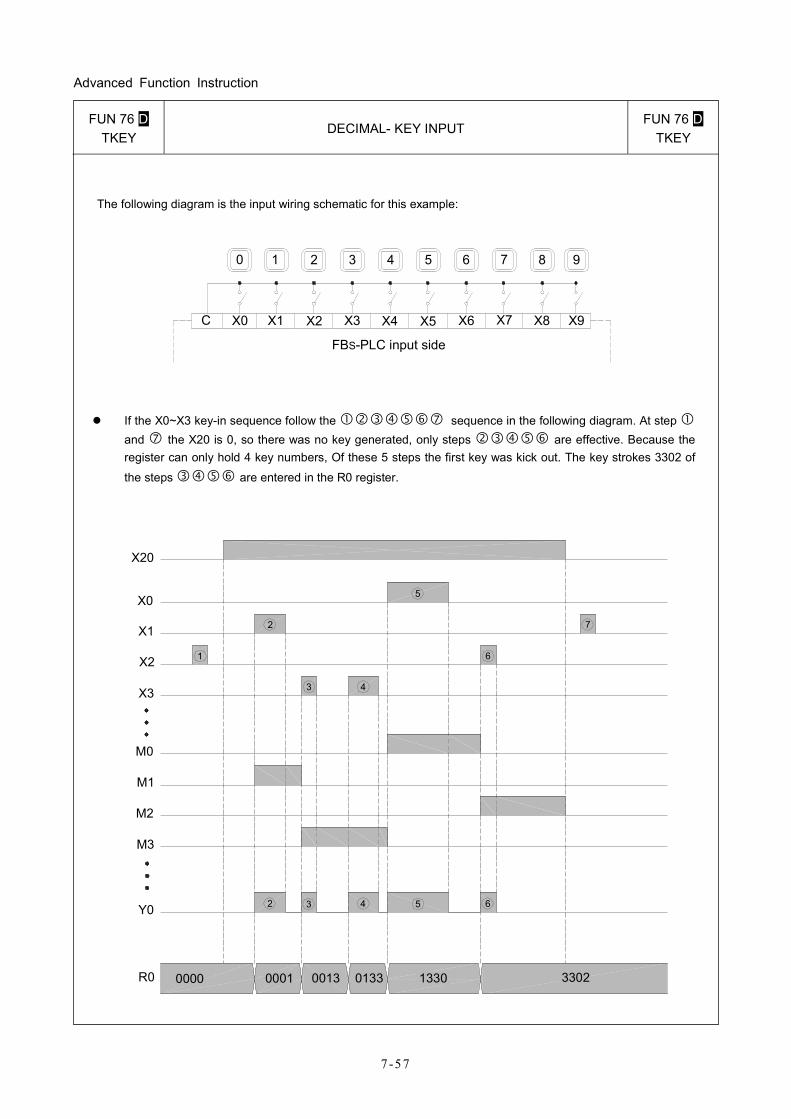
Advanced Function Instruction
7-57
FUN 76 D TKEY
DECIMAL- KEY INPUT FUN 76 D
TKEY
The following diagram is the input wiring schematic for this example:
0 1 2 3 4 5 6 7 8 9
C X0 X1 X2 X3 X4 X5 X6 X7 X8 X9
FBS-PLC input side
If the X0~X3 key-in sequence follow the sequence in the following diagram. At step and the X20 is 0, so there was no key generated, only steps are effective. Because the register can only hold 4 key numbers, Of these 5 steps the first key was kick out. The key strokes 3302 of
the steps are entered in the R0 register.
X20
X0
X1
X2
X3
M0
M1
M2
M3
Y0
R0 0000 0001 0013 1330 3302
3 4 5 6
1
2
4
6
0000 0001 0013 0133 1330 33020000 0001 0013 0133 1330 3302
2
5
7
6
43
1
2 3 4 5 6
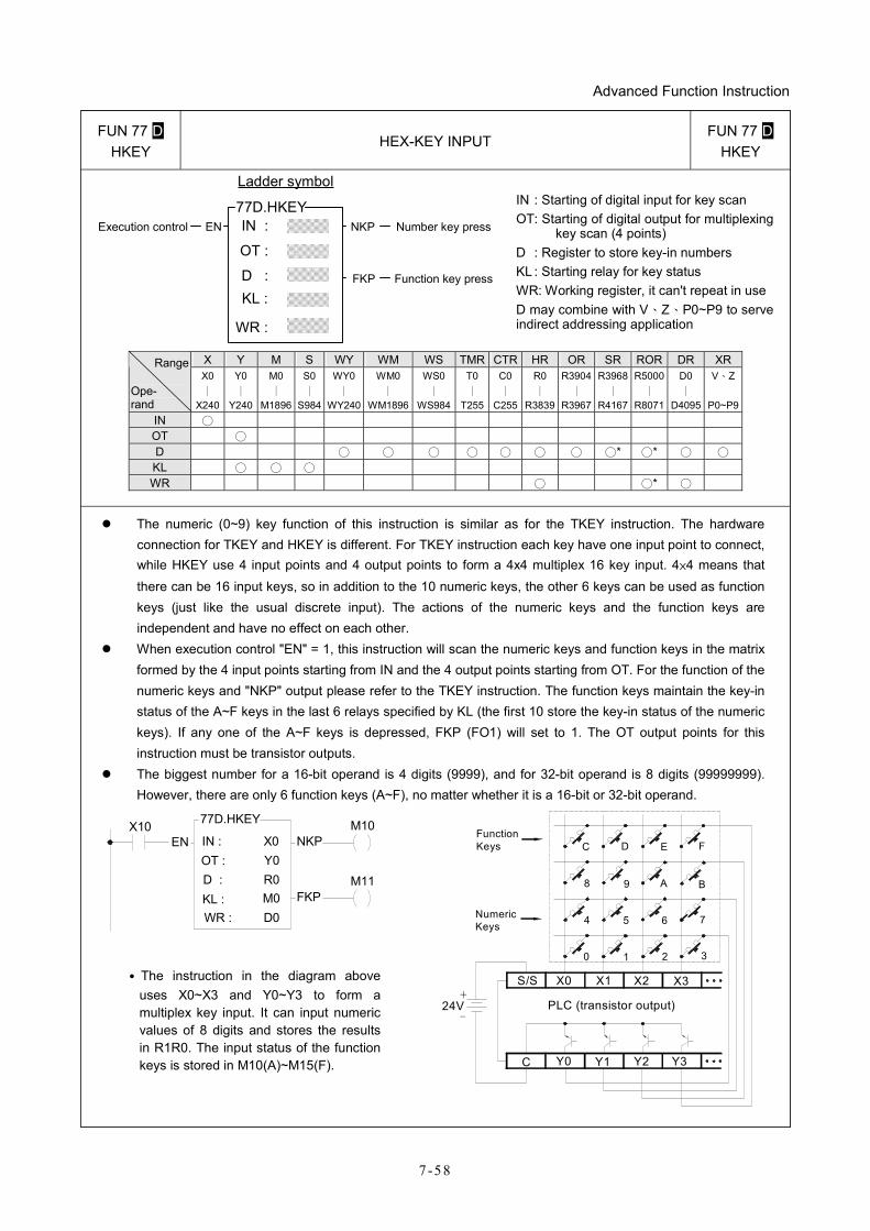
Advanced Function Instruction
7 -58
FUN 77 D HKEY
HEX-KEY INPUT FUN 77 D
HKEY
IN :
D :
ENExecution control
Ladder symbol
77D.HKEY
OT :
FKP Function key press
NKP Number key press
KL :
WR :
IN : Starting of digital input for key scan OT: Starting of digital output for multiplexing
key scan (4 points) D : Register to store key-in numbers KL : Starting relay for key status WR: Working register, it can't repeat in use D may combine with V、Z、P0~P9 to serve indirect addressing application
X Y M S WY WM WS TMR CTR HR OR SR ROR DR XRRange
Ope- rand
X0 ∣
X240
Y0 ∣
Y240
M0 ∣
M1896
S0 ∣
S984
WY0 ∣
WY240
WM0 ∣
WM1896
WS0∣
WS984
T0∣
T255
C0∣
C255
R0 ∣
R3839
R3904∣
R3967
R3968 ∣
R4167
R5000 ∣
R8071
D0 ∣
D4095
V、Z
P0~P9IN ○ OT ○ D ○ ○ ○ ○ ○ ○ ○ ○* ○* ○ ○
KL ○ ○ ○ WR ○ ○* ○
The numeric (0~9) key function of this instruction is similar as for the TKEY instruction. The hardware connection for TKEY and HKEY is different. For TKEY instruction each key have one input point to connect, while HKEY use 4 input points and 4 output points to form a 4x4 multiplex 16 key input. 4×4 means that there can be 16 input keys, so in addition to the 10 numeric keys, the other 6 keys can be used as function keys (just like the usual discrete input). The actions of the numeric keys and the function keys are independent and have no effect on each other.
When execution control "EN" = 1, this instruction will scan the numeric keys and function keys in the matrix formed by the 4 input points starting from IN and the 4 output points starting from OT. For the function of the numeric keys and "NKP" output please refer to the TKEY instruction. The function keys maintain the key-in status of the A~F keys in the last 6 relays specified by KL (the first 10 store the key-in status of the numeric keys). If any one of the A~F keys is depressed, FKP (FO1) will set to 1. The OT output points for this instruction must be transistor outputs.
The biggest number for a 16-bit operand is 4 digits (9999), and for 32-bit operand is 8 digits (99999999). However, there are only 6 function keys (A~F), no matter whether it is a 16-bit or 32-bit operand.
EN IN :X10 77D.HKEY
OT :D : R0
Y0X0
M0D0WR :
KL :
NKPM10
FKPM11
˙ The instruction in the diagram above uses X0~X3 and Y0~Y3 to form a multiplex key input. It can input numeric values of 8 digits and stores the results in R1R0. The input status of the function keys is stored in M10(A)~M15(F). C Y0 Y1 Y2 Y3
S/S X0
PLC (transistor output)
C D E F
8 9 A B
4 5 6 7
0 1 2 3
FunctionKeys
NumericKeys
X1 X2 X3
24V-
+
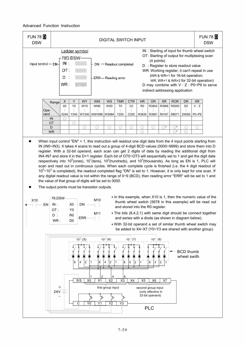
Advanced Function Instruction
7-59
FUN 78 D DSW
DIGITAL SWITCH INPUT FUN 78 D
DSW
IN : Starting of input for thumb wheel switch OT : Starting of output for multiplexing scan
(4 points) D : Register to store readout value WR: Working register, it can't repeat in use (WR & WR+1 for 16-bit operation;
WR, WR+1 & WR+2 for 32-bit operation) D may combine with V、Z、P0~P9 to serve indirect addressing application
X Y WY WM WS TMR CTR HR OR SR ROR DR XR Range
Ope- rand
X0 ∣
X240
Y0∣
Y240
WY0 ∣
WY240
WM0 ∣
WM1896
WS0∣
WS984
T0 ∣
T255
C0 ∣
C255
R0 ∣
R3839
R3904∣
R3967
R3968∣
R4167
R5000 ∣
R8071
D0 ∣
D4095
V、Z
P0~P9 IN ○ OT ○ D ○ ○ ○ ○ ○ ○ ○ ○* ○* ○ ○
WR ○ ○* ○
When input control "EN" = 1, this instruction will readout one digit data from the 4 input points starting from IN (IN0~IN3). It takes 4 scans to read out a group of 4-digit BCD values (0000~9999) and store them into D register. With a 32-bit operand, each scan can get 2 digits of data by reading the additional digit from IN4-IN7 and store it in the D+1 register. Each bit of OT0~OT3 will sequentially set to 1 and get the digit data respectively into 100(ones), 101(tens), 102(hundreds), and 103(thousands). As long as EN is 1, PLC will scan and read out in continuous cycles. When each complete cycle is finished (i.e. the 4 digit readout of 100~103 is completed), the readout completed flag "DN" is set to 1. However, it is only kept for one scan. If any digital readout value is not within the range of 0~9 (BCD), then reading error "ERR" will be set to 1 and the value of that group of digits will be set to 0000.
The output points must be transistor outputs.
X10EN IN : X0
M10
OT : Y0R0D :D0WR :
M11
DN
ERR
78.DSW
˙In this example, when X10 is 1, then the numeric value of the thumb wheel switch (5678 in this example) will be read out and stored into the R0 register.
˙The bits (8,4,2,1) with same digit should be connect together and series with a diode (as shown in diagram below).
˙With 32-bit operand a set of similar thumb wheel switch may be added to X4~X7 (Y0~Y3 are shared with another group).
8
BCD thumbwheel swith
first group input
Y1Y0C Y2 Y3
X1X0S/S1
24 1
4X2
2X3
8
second group input(only effective in 32-bit operand)
PLC
X4 X5 X6 X7
3 (5)10 2 (6)10 101 (7) (8)100
24V
1248 1248 1248
-
+
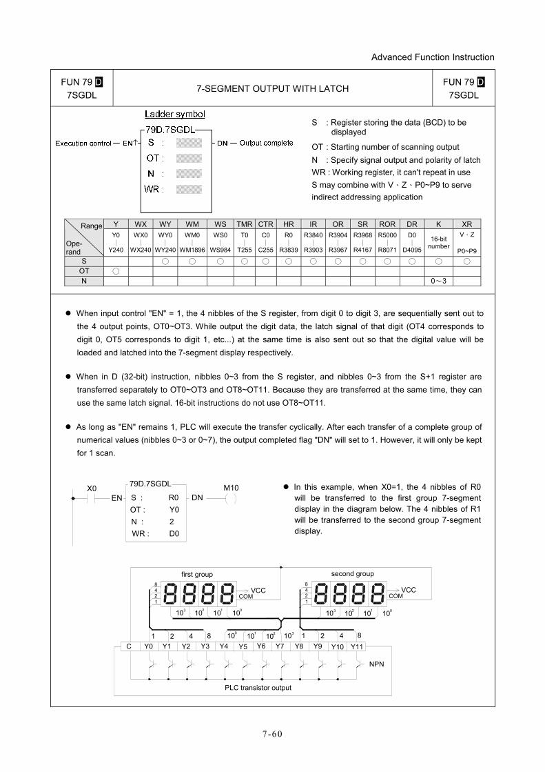
Advanced Function Instruction
7 -60
FUN 79 D 7SGDL
7-SEGMENT OUTPUT WITH LATCH FUN 79 D
7SGDL
S : Register storing the data (BCD) to be displayed
OT : Starting number of scanning output N : Specify signal output and polarity of latch WR : Working register, it can't repeat in use S may combine with V、Z、P0~P9 to serve indirect addressing application
Y WX WY WM WS TMR CTR HR IR OR SR ROR DR K XR Range
Ope- rand
Y0 ∣
Y240
WX0 ∣
WX240
WY0 ∣
WY240
WM0 ∣
WM1896
WS0∣
WS984
T0∣
T255
C0∣
C255
R0 ∣
R3839
R3840∣
R3903
R3904∣
R3967
R3968∣
R4167
R5000 ∣
R8071
D0 ∣
D4095
16-bit number
V、Z
P0~P9S ○ ○ ○ ○ ○ ○ ○ ○ ○ ○ ○ ○ ○
OT ○ N 0~3
When input control "EN" = 1, the 4 nibbles of the S register, from digit 0 to digit 3, are sequentially sent out to the 4 output points, OT0~OT3. While output the digit data, the latch signal of that digit (OT4 corresponds to digit 0, OT5 corresponds to digit 1, etc...) at the same time is also sent out so that the digital value will be loaded and latched into the 7-segment display respectively.
When in D (32-bit) instruction, nibbles 0~3 from the S register, and nibbles 0~3 from the S+1 register are transferred separately to OT0~OT3 and OT8~OT11. Because they are transferred at the same time, they can use the same latch signal. 16-bit instructions do not use OT8~OT11.
As long as "EN" remains 1, PLC will execute the transfer cyclically. After each transfer of a complete group of numerical values (nibbles 0~3 or 0~7), the output completed flag "DN" will set to 1. However, it will only be kept for 1 scan.
EN DNM10
OT : Y0
WR : D0
X0 79D.7SGDL
N :
S : R0
2
In this example, when X0=1, the 4 nibbles of R0 will be transferred to the first group 7-segment display in the diagram below. The 4 nibbles of R1 will be transferred to the second group 7-segment display.
first group second group
VCC VCCCOMCOM
1248 8
421
103 102
PLC transistor output
NPN
101 100 10 10 10 100123
1 2 4 8 010 8421110 102 103
C Y0 Y1 Y2 Y3 Y4 Y5 Y6 Y7 Y8 Y9 Y10 Y11
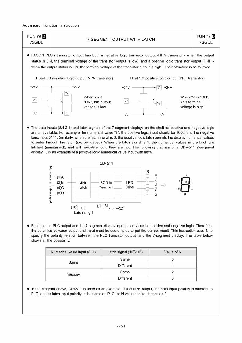
Advanced Function Instruction
7-61
FUN 79 D 7SGDL
7-SEGMENT OUTPUT WITH LATCH FUN 79 D
7SGDL
FACON PLC's transistor output has both a negative logic transistor output (NPN transistor - when the output status is ON, the terminal voltage of the transistor output is low), and a positive logic transistor output (PNP - when the output status is ON, the terminal voltage of the transistor output is high). Their structure is as follows:
FBs-PLC negative logic output (NPN transistor) FBs-PLC positive logic output (PNP transistor)
+24V
0V
Yn
Yn
C
+24V
When Yn is "ON", this output voltage is low
+24V
0V
YnYn
C +24V
0V
When Yn is "ON", Yn's terminal voltage is high
The data inputs (8,4,2,1) and latch signals of the 7-segment displays on the shelf for positive and negative logic are all available. For example, for numerical value "8", the positive logic input should be 1000, and the negative logic input 0111. Similarly, when the latch signal is 0, the positive logic latch permits the display numerical values to enter through the latch (i.e. be loaded). When the latch signal is 1, the numerical values in the latch are latched (maintained), and with negative logic they are not. The following diagram of a CD-4511 7-segment display IC is an example of a positive logic numerical value input with latch.
4bitlatch
BCD to7-segment
LEDDrive
CD4511
(1)A(2)B(4)C(8)D
(10 ) LELatch sing 1
LT BIVCC
Rabcdefg
Num
berical value input
n
a
g
d
f
e
b
c
Because the PLC output and the 7-segment display input polarity can be positive and negative logic. Therefore, the polarities between output and input must be coordinated to get the correct result. This instruction uses N to specify the polarity relation between the PLC transistor output, and the 7-segment display. The table below shows all the possibility.
Numerical value input (8~1) Latch signal (100-103) Value of N
Same 0 Same
Different 1
Same 2 Different
Different 3
In the diagram above, CD4511 is used as an example. If use NPN output, the data input polarity is different to PLC, and its latch input polarity is the same as PLC, so N value should chosen as 2.
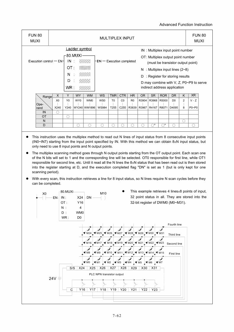
Advanced Function Instruction
7 -62
FUN 80 MUXI
MULTIPLEX INPUT FUN 80 MUXI
IN : Multiplex input point number
OT : Multiplex output point number (must be transistor output point)
N : Multiplex input lines (2~8)
D : Register for storing results
D may combine with V, Z, P0~P9 to serve indirect address application
X Y WY WM WS TMR CTR HR OR SR ROR DR K XRRange
Ope- rand
X0 ∣
X240
Y0 ∣
Y240
WY0 ∣
WY240
WM0 ∣
WM1896
WS0 ∣
WS984
T0 ∣
T255
C0∣
C255
R0 ∣
R3839
R3904∣
R3967
R3968∣
R4167
R5000 ∣
R8071
D0 ∣
D4095
2 ∣ 8
V、Z
P0~P0
IN ○ OT ○ N ○ D ○ ○ ○ ○ ○ ○ ○ ○* ○* ○ ○
This instruction uses the multiplex method to read out N lines of input status from 8 consecutive input points (IN0~IN7) starting from the input point specified by IN. With this method we can obtain 8×N input status, but only need to use 8 input points and N output points.
The multiplex scanning method goes through N output points starting from the OT output point. Each scan one of the N bits will set to 1 and the corresponding line will be selected. OT0 responsible for first line, while OT1 responsible for second line, etc. Until it read all the N lines the 8×N status that has been read out is then stored into the register starting at D, and the execution completed flag "DN" is set as 1 (but is only kept for one scanning period).
With every scan, this instruction retrieves a line for 8 input status, so N lines require N scan cycles before they can be completed.
EN IN : X24
80.MUXI
DNM10
OT : Y164N :
WR : D0WM0D :
X0
This example retrieves 4 lines×8 points of input, 32 point status in all. They are stored into the 32-bit register of DWM0 (M0~M31).
Fourth line
Third line
Second line
First line
M24 M25 M26 M27 M28 M29 M30 M31
M16 M17 M18 M19 M20 M21 M22 M23
M8 M9 M10
M0 M1 M2
M11
M3 M4
M12
M5
M13 M14
M6 M7
M15
PLC NPN transistor output
S/S X24 X25 X26 X27 X28 X29 X30 X31
C Y16 Y17 Y18 Y19 Y20 Y21 Y22 Y23
24V
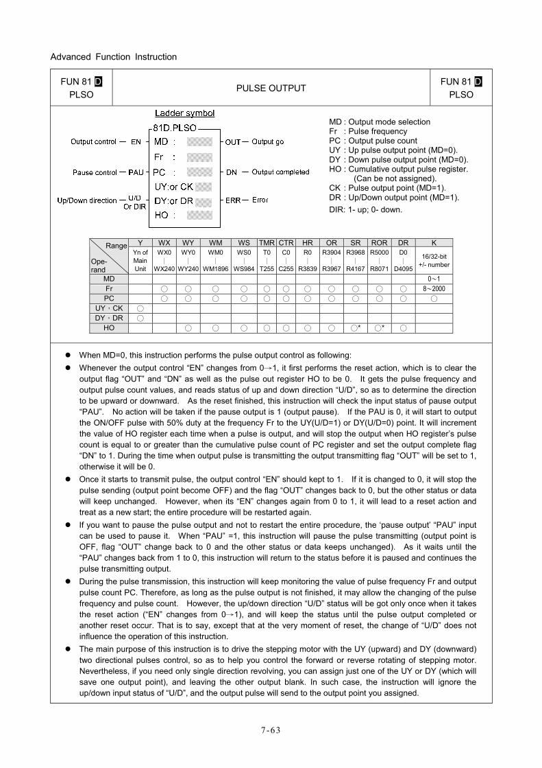
Advanced Function Instruction
7-63
FUN 81 D PLSO
PULSE OUTPUT FUN 81 D
PLSO
MD : Output mode selection Fr : Pulse frequency PC : Output pulse count UY : Up pulse output point (MD=0). DY : Down pulse output point (MD=0). HO : Cumulative output pulse register.
(Can be not assigned). CK : Pulse output point (MD=1). DR : Up/Down output point (MD=1). DIR: 1- up; 0- down.
Y WX WY WM WS TMR CTR HR OR SR ROR DR K Range
Ope- rand
Yn of Main Unit
WX0 ∣
WX240
WY0 ∣
WY240
WM0 ∣
WM1896
WS0∣
WS984
T0∣
T255
C0∣
C255
R0 ∣
R3839
R3904∣
R3967
R3968∣
R4167
R5000 ∣
R8071
D0 ∣
D4095
16/32-bit +/- number
MD 0~1 Fr ○ ○ ○ ○ ○ ○ ○ ○ ○ ○ ○ 8~2000 PC ○ ○ ○ ○ ○ ○ ○ ○ ○ ○ ○ ○
UY,CK ○ DY,DR ○
HO ○ ○ ○ ○ ○ ○ ○ ○* ○* ○
When MD=0, this instruction performs the pulse output control as following: Whenever the output control “EN” changes from 0→1, it first performs the reset action, which is to clear the
output flag “OUT” and “DN” as well as the pulse out register HO to be 0. It gets the pulse frequency and output pulse count values, and reads status of up and down direction “U/D”, so as to determine the direction to be upward or downward. As the reset finished, this instruction will check the input status of pause output “PAU”. No action will be taken if the pause output is 1 (output pause). If the PAU is 0, it will start to output the ON/OFF pulse with 50% duty at the frequency Fr to the UY(U/D=1) or DY(U/D=0) point. It will increment the value of HO register each time when a pulse is output, and will stop the output when HO register’s pulse count is equal to or greater than the cumulative pulse count of PC register and set the output complete flag “DN” to 1. During the time when output pulse is transmitting the output transmitting flag “OUT” will be set to 1, otherwise it will be 0.
Once it starts to transmit pulse, the output control “EN” should kept to 1. If it is changed to 0, it will stop the pulse sending (output point become OFF) and the flag “OUT” changes back to 0, but the other status or data will keep unchanged. However, when its “EN” changes again from 0 to 1, it will lead to a reset action and treat as a new start; the entire procedure will be restarted again.
If you want to pause the pulse output and not to restart the entire procedure, the ‘pause output’ “PAU” input can be used to pause it. When “PAU” =1, this instruction will pause the pulse transmitting (output point is OFF, flag “OUT” change back to 0 and the other status or data keeps unchanged). As it waits until the “PAU” changes back from 1 to 0, this instruction will return to the status before it is paused and continues the pulse transmitting output.
During the pulse transmission, this instruction will keep monitoring the value of pulse frequency Fr and output pulse count PC. Therefore, as long as the pulse output is not finished, it may allow the changing of the pulse frequency and pulse count. However, the up/down direction “U/D” status will be got only once when it takes the reset action (“EN” changes from 0→1), and will keep the status until the pulse output completed or another reset occur. That is to say, except that at the very moment of reset, the change of “U/D” does not influence the operation of this instruction.
The main purpose of this instruction is to drive the stepping motor with the UY (upward) and DY (downward) two directional pulses control, so as to help you control the forward or reverse rotating of stepping motor. Nevertheless, if you need only single direction revolving, you can assign just one of the UY or DY (which will save one output point), and leaving the other output blank. In such case, the instruction will ignore the up/down input status of “U/D”, and the output pulse will send to the output point you assigned.
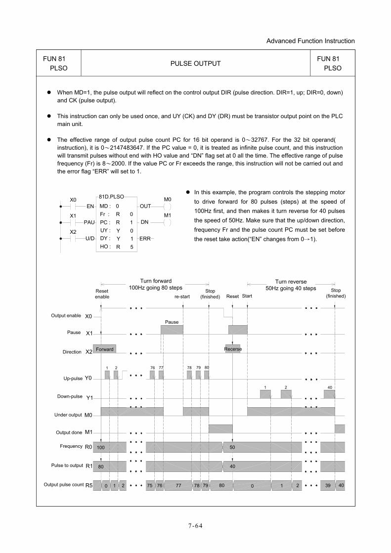
Advanced Function Instruction
7 -64
FUN 81 PLSO
PULSE OUTPUT FUN 81
PLSO
When MD=1, the pulse output will reflect on the control output DIR (pulse direction. DIR=1, up; DIR=0, down) and CK (pulse output).
This instruction can only be used once, and UY (CK) and DY (DR) must be transistor output point on the PLC main unit.
The effective range of output pulse count PC for 16 bit operand is 0~32767. For the 32 bit operand( instruction), it is 0~2147483647. If the PC value = 0, it is treated as infinite pulse count, and this instruction will transmit pulses without end with HO value and “DN” flag set at 0 all the time. The effective range of pulse frequency (Fr) is 8~2000. If the value PC or Fr exceeds the range, this instruction will not be carried out and the error flag “ERR” will set to 1.
X0EN MD : 0
81D.PLSO
OUTM0
Fr : R 0PC :
DY :UY :
HO :
X1PAU
X2U/D
DNM1
R 1Y 0Y 1R 5
ERR
In this example, the program controls the stepping motor to drive forward for 80 pulses (steps) at the speed of 100Hz first, and then makes it turn reverse for 40 pulses the speed of 50Hz. Make sure that the up/down direction, frequency Fr and the pulse count PC must be set before the reset take action(“EN” changes from 0→1).
Turn forward100Hz going 80 stepsReset
enable
X0
X1
X2
Pause
re-startStop
(finished)
Y0
Turn reverse50Hz going 40 steps
Reset StartStop
(finished)
Y1
M0
M1
R0
R1
R5Output pulse count
Pulse to output
Frequency
Output done
Under output
Down-pulse
Output enable
Pause
Direction
Up-pulse
Recerse
1 2 76 77 78 79 80
1 2 40
100
80
0 1 2 75 76 77 78 79 80
50
40
0 1 2 39 40
Forward
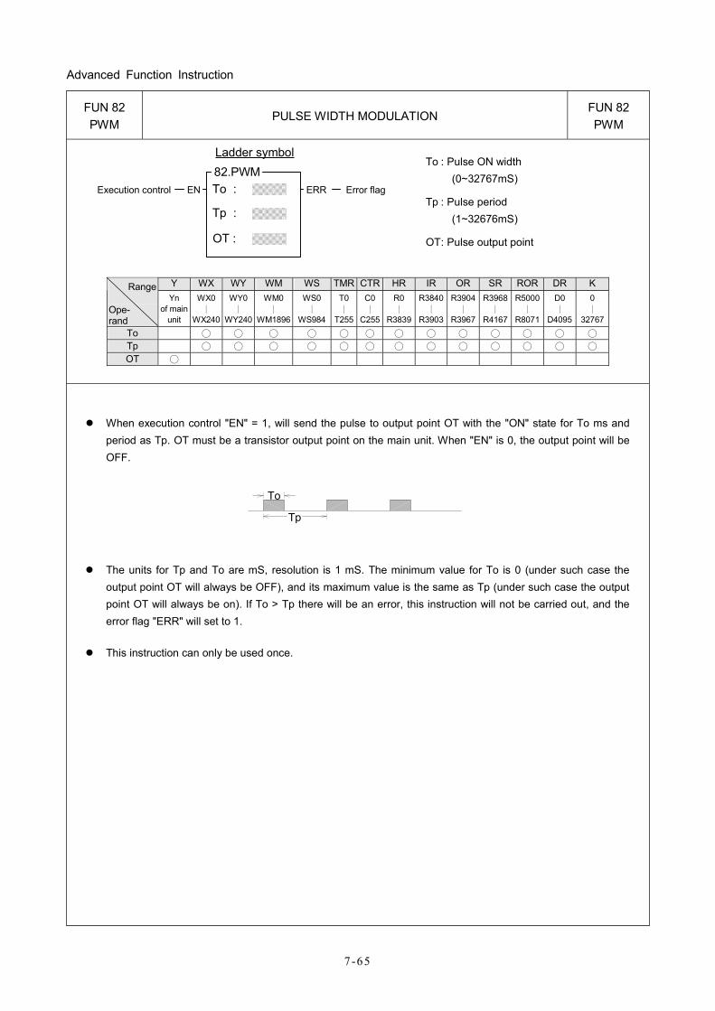
Advanced Function Instruction
7-65
FUN 82 PWM
PULSE WIDTH MODULATION FUN 82 PWM
To :ENExecution control
Ladder symbol 82.PWM
Tp :
ERR
OT :
Error flag
To : Pulse ON width (0~32767mS)
Tp : Pulse period (1~32676mS)
OT : Pulse output point
Y WX WY WM WS TMR CTR HR IR OR SR ROR DR K Range
Ope- rand
Yn of main
unit
WX0∣
WX240
WY0 ∣
WY240
WM0 ∣
WM1896
WS0 ∣
WS984
T0∣
T255
C0∣
C255
R0 ∣
R3839
R3840∣
R3903
R3904∣
R3967
R3968 ∣
R4167
R5000 ∣
R8071
D0 ∣
D4095
0 ∣
32767To ○ ○ ○ ○ ○ ○ ○ ○ ○ ○ ○ ○ ○ Tp ○ ○ ○ ○ ○ ○ ○ ○ ○ ○ ○ ○ ○ OT ○
When execution control "EN" = 1, will send the pulse to output point OT with the "ON" state for To ms and period as Tp. OT must be a transistor output point on the main unit. When "EN" is 0, the output point will be OFF.
To
Tp
The units for Tp and To are mS, resolution is 1 mS. The minimum value for To is 0 (under such case the output point OT will always be OFF), and its maximum value is the same as Tp (under such case the output point OT will always be on). If To > Tp there will be an error, this instruction will not be carried out, and the error flag "ERR" will set to 1.
This instruction can only be used once.
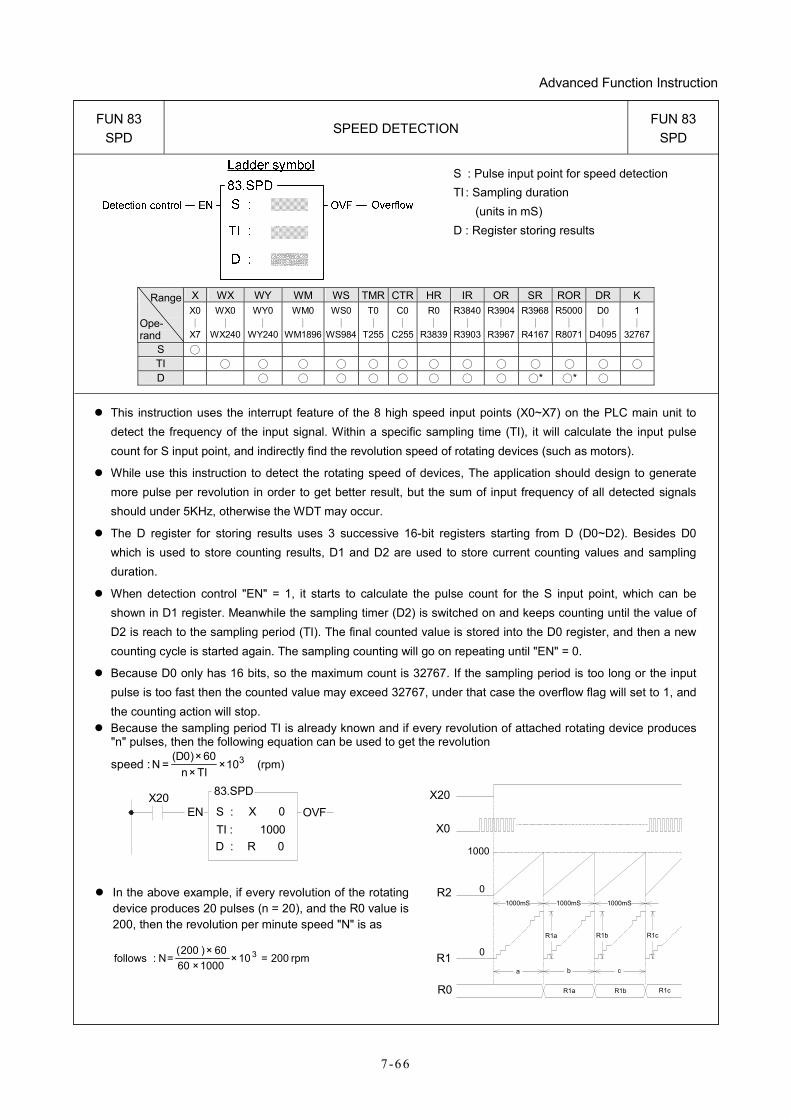
Advanced Function Instruction
7 -66
FUN 83 SPD
SPEED DETECTION FUN 83
SPD
S : Pulse input point for speed detection TI : Sampling duration
(units in mS) D : Register storing results
X WX WY WM WS TMR CTR HR IR OR SR ROR DR K Range
Ope- rand
X0 ∣ X7
WX0∣
WX240
WY0 ∣
WY240
WM0 ∣
WM1896
WS0∣
WS984
T0∣
T255
C0∣
C255
R0 ∣
R3839
R3840∣
R3903
R3904∣
R3967
R3968∣
R4167
R5000 ∣
R8071
D0 ∣
D4095
1 ∣
32767 S ○ TI ○ ○ ○ ○ ○ ○ ○ ○ ○ ○ ○ ○ ○ D ○ ○ ○ ○ ○ ○ ○ ○ ○* ○* ○
This instruction uses the interrupt feature of the 8 high speed input points (X0~X7) on the PLC main unit to detect the frequency of the input signal. Within a specific sampling time (TI), it will calculate the input pulse count for S input point, and indirectly find the revolution speed of rotating devices (such as motors).
While use this instruction to detect the rotating speed of devices, The application should design to generate more pulse per revolution in order to get better result, but the sum of input frequency of all detected signals should under 5KHz, otherwise the WDT may occur.
The D register for storing results uses 3 successive 16-bit registers starting from D (D0~D2). Besides D0 which is used to store counting results, D1 and D2 are used to store current counting values and sampling duration.
When detection control "EN" = 1, it starts to calculate the pulse count for the S input point, which can be shown in D1 register. Meanwhile the sampling timer (D2) is switched on and keeps counting until the value of D2 is reach to the sampling period (TI). The final counted value is stored into the D0 register, and then a new counting cycle is started again. The sampling counting will go on repeating until "EN" = 0.
Because D0 only has 16 bits, so the maximum count is 32767. If the sampling period is too long or the input pulse is too fast then the counted value may exceed 32767, under that case the overflow flag will set to 1, and the counting action will stop.
Because the sampling period TI is already known and if every revolution of attached rotating device produces "n" pulses, then the following equation can be used to get the revolution
speed : )rpm(10×TI×n60×)0D(
=N 3
X20EN S : X 0
83.SPD
D : R 0TI : 1000
OVF
In the above example, if every revolution of the rotating device produces 20 pulses (n = 20), and the R0 value is 200, then the revolution per minute speed "N" is as
rpm200=10×1000×60
60×)200(=N:follows 3
1000mS 1000mS 1000mS
R1a R1b R1c
a b c
R1a R1b R1c
1000
0
0
X0
R2
R1
R0
X20
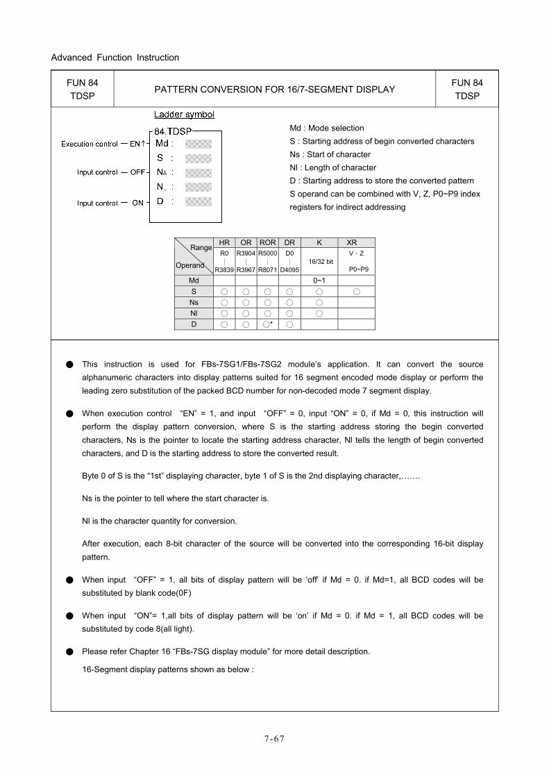
Advanced Function Instruction
7-67
FUN 84 TDSP
PATTERN CONVERSION FOR 16/7-SEGMENT DISPLAY FUN 84 TDSP
Md : Mode selection S : Starting address of begin converted characters Ns : Start of character Nl : Length of character D : Starting address to store the converted pattern S operand can be combined with V, Z, P0~P9 index registers for indirect addressing
HR OR ROR DR K XR
Range Operand
R0∣
R3839
R3904∣
R3967
R5000∣
R8071
D0∣
D409516/32 bit
V、Z P0~P9
Md 0~1 S ○ ○ ○ ○ ○ ○ Ns ○ ○ ○ ○ ○ Nl ○ ○ ○ ○ ○ D ○ ○ ○* ○
● This instruction is used for FBs-7SG1/FBs-7SG2 module’s application. It can convert the source alphanumeric characters into display patterns suited for 16 segment encoded mode display or perform the leading zero substitution of the packed BCD number for non-decoded mode 7 segment display.
● When execution control “EN” = 1, and input “OFF” = 0, input “ON” = 0, if Md = 0, this instruction will perform the display pattern conversion, where S is the starting address storing the begin converted characters, Ns is the pointer to locate the starting address character, Nl tells the length of begin converted characters, and D is the starting address to store the converted result.
Byte 0 of S is the “1st” displaying character, byte 1 of S is the 2nd displaying character,…….
Ns is the pointer to tell where the start character is.
Nl is the character quantity for conversion.
After execution, each 8-bit character of the source will be converted into the corresponding 16-bit display pattern.
● When input “OFF” = 1, all bits of display pattern will be ‘off’ if Md = 0. if Md=1, all BCD codes will be substituted by blank code(0F)
● When input “ON”= 1,all bits of display pattern will be ‘on’ if Md = 0. if Md = 1, all BCD codes will be substituted by code 8(all light).
● Please refer Chapter 16 “FBs-7SG display module” for more detail description.
16-Segment display patterns shown as below :
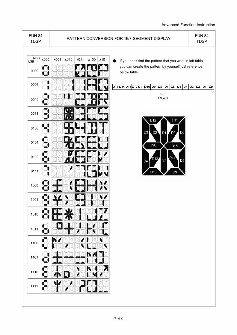
Advanced Function Instruction
7 -68
FUN 84 TDSP
PATTERN CONVERSION FOR 16/7-SEGMENT DISPLAY FUN 84 TDSP
x000 x001 x010 x011 x100 x101
0000
0001
0010
0011
0100
0101
0110
0111
1000
1001
1010
1011
1100
1101
1110
1111
MSBLSB
● If you don’t find the pattern that you want in left table, you can create the pattern by yourself just reference below table.
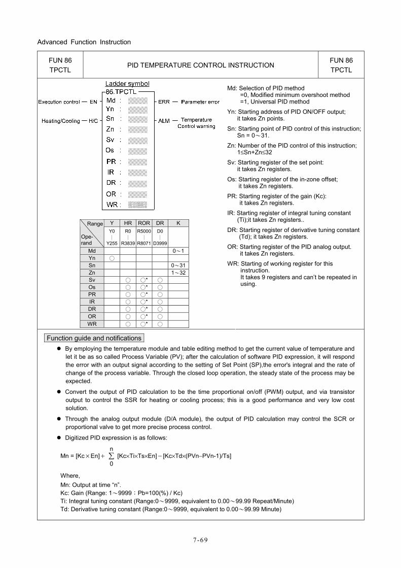
Advanced Function Instruction
7-69
FUN 86 TPCTL
PID TEMPERATURE CONTROL INSTRUCTION FUN 86 TPCTL
Function guide and notifications
By employing the temperature module and table editing method to get the current value of temperature and let it be as so called Process Variable (PV); after the calculation of software PID expression, it will respond the error with an output signal according to the setting of Set Point (SP),the error's integral and the rate of change of the process variable. Through the closed loop operation, the steady state of the process may be expected.
Convert the output of PID calculation to be the time proportional on/off (PWM) output, and via transistor output to control the SSR for heating or cooling process; this is a good performance and very low cost solution.
Through the analog output module (D/A module), the output of PID calculation may control the SCR or proportional valve to get more precise process control.
Digitized PID expression is as follows:
Mn = [Kc×En]+ ∑0
n [Kc×Ti×Ts×En]−[Kc×Td×(PVn−PVn-1)/Ts]
Where, Mn: Output at time “n”. Kc: Gain (Range: 1~9999;Pb=100(%) / Kc) Ti: Integral tuning constant (Range:0~9999, equivalent to 0.00~99.99 Repeat/Minute) Td: Derivative tuning constant (Range:0~9999, equivalent to 0.00~99.99 Minute)
Md: Selection of PID method =0, Modified minimum overshoot method =1, Universal PID method
Yn: Starting address of PID ON/OFF output; it takes Zn points.
Sn: Starting point of PID control of this instruction;Sn = 0~31.
Zn: Number of the PID control of this instruction; 1≤Sn+Zn≤32
Sv: Starting register of the set point: it takes Zn registers.
Os: Starting register of the in-zone offset; it takes Zn registers.
PR: Starting register of the gain (Kc): it takes Zn registers.
IR: Starting register of integral tuning constant (Ti);it takes Zn registers..
DR: Starting register of derivative tuning constant (Td); it takes Zn registers.
OR: Starting register of the PID analog output. it takes Zn registers.
WR: Starting of working register for this instruction. It takes 9 registers and can’t be repeated in using.
Y HR ROR DR K Range
Ope- rand
Y0 ∣
Y255
R0 ∣
R3839
R5000 ∣
R8071
D0 ∣
D3999
Md 0~1Yn ○ Sn 0~31Zn 1~32Sv ○ ○* ○ Os ○ ○* ○ PR ○ ○* ○ IR ○ ○* ○ DR ○ ○* ○ OR ○ ○* ○ WR ○ ○* ○
Advanced Function Instruction
7 -70
FUN 86 TPCTL
PID TEMPERATURE CONTROL INSTRUCTION FUN 86 TPCTL
PVn : Process variable at time “n” PVn_1: Process variable when loop was last solved En: Error at time “n” ; E= SP – PVn Ts: Solution interval for PID calculation (Valid value are 10, 20, 40, 80,160, 320; the unit is in 0.1Sec)
PID Parameter Adjustment Guide
As the gain (Kc) adjustment getting larger, the larger the proportional contribution to the output. This can obtain a sensitive and rapid control reaction. However, when the gain is too large, it may cause oscillation. Do the best to adjust “Kc” larger (but not to the extent of making oscillation), which could increase the process reaction and reduce the steady state error.
Integral item may be used to eliminate the steady state error. The larger the number (Ti, integral tuning constant), the larger the integral contribution to the output. When there is steady state error, adjust the “Ti” larger to decrease the error. When the “Ti” = 0, the integral item makes no contribution to the output. For exam. , if the reset time is 6 minutes, Ti=100/6=17;if the integral time is 5 minutes, Ti=100/5=20.
Derivative item may be used to make the process smoother and not too over shoot. The larger the number (Td, derivative tuning constant), the larger the derivative contribution to the output. When there is too over shoot, adjust the “Td” larger to decrease the amount of over shoot. When the “Td” = 0, the derivative item makes no contribution to the output. For exa, if the rate time is 1 minute, then the Td = 100; if the differential time is 2 minute, then the Td = 200.
Properly adjust the PID parameters can obtain an excellent result for temperature control.
The default solution interval for PID calculation is 4 seconds (Ts=40)
The default of gain value (Kc) is 110, where Pb=1000/110×0.1%≒0.91%; the system full range is 1638°, it means 1638×0.91≒14.8°to enter proportional band control.
The default of integral tuning constant is 17, it means the reset time is 6 minutes (Ti=100/6=17).
The default of derivative tuning constant is 50, it means the rate time is 0.5 minutes (Td=50).
When changing the PID solution interval, it may tune the parameters Kc, Ti, Td again.
Instruction guide
FUN86 will be enabled after reading all temperature channels.
When execution control “EN” = 1, it depends on the input status of H/C for PID operation to make heating (H/C=1) or cooling (H/C=0) control. The current values of measured temperature are through the multiplexing temperature module ; the set points of desired temperature are stored in the registers starting from Sv. With the calculation of software PID expression, it will respond the error with an output signal according to the setting of set point, the error's integral and the rate of change of the process variable. Convert the output of PID calculation to be the time proportional on/off (PWM) output, and via transistor output to control the SSR for heating or cooling process; where there is a good performance and very low cost solution. It may also apply the output of PID calculation (stored in registers starting from OR), by way of D/A analog output module, to control SCR or proportional valve, so as to get more precise process control.
When the setting of Sn, Zn (0 Sn 31 and 1 Zn 32, as well as 1 Sn + Zn 32) comes error, this instruction will not be executed and the instruction output “ERR” will be ON.
This instruction compares the current value with the set point to check whether the current temperature falls within deviation range (stored in register starting from Os). If it falls in the deviation range, it will set the in-zone bit of that point to be ON; if not, clear the in-zone bit of that point to be OFF, and make instruction output “ALM” to be ON.
Advanced Function Instruction
7-71
FUN 86 TPCTL
PID TEMPERATURE CONTROL INSTRUCTION FUN 86 TPCTL
In the mean time, this instruction will also check whether highest temperature warning (the register for the set point of highest temperature warning is R4008). When successively scanning for ten times the current values of measured temperature are all higher than or equal to the highest warning set point, the warning bit will set to be ON and instruction output “ALM” will be on. This can avoid the safety problem aroused from temperature out of control, in case the SSR or heating circuit becomes short.
This instruction can also detect the unable to heat problem resulting from the SSR or heating circuit runs open, or the obsolete heating band. When output of temperature control turns to be large power (set in R4006 register) successively in a certain time (set in R4007 register), and can not make current temperature fall in desired range, the warning bit will set to be ON and instruction output “ALM” will be ON.
WR: Starting of working register for this instruction. It takes 9 registers and can’t be repeated in using. The content of the two registers WR+0 and WR+1 indicating that whether the current temperature falls
within the deviation range (stored in registers starting from Os). If it falls in the deviation range, the in-zone bit of that point will be set ON; if not, the in-zone bit of that point will be cleared OFF. Bit definition of WR+0 explained as follows: Bit0=1, it represents that the temperature of the Sn+0 point is in-zone… Bit15=1, it represents that the temperature of the Sn+15 point is in-zone.
Bit definition of WR+1 explained as follows: Bit0=1, it represents that the temperature of the Sn+16 point is in-zone… Bit15=1, it represents that the temperature of Sn+31 point is in-zone. The content of the two registers WR+2 and WR+3 are the warning bit registers, they indicate that whether there exists the highest temperature warning or heating circuit opened.
Bit definition of WR+2 explained as follows: Bit0=1, it means that there exists the highest warning or heating circuit opened at the Sn+0 point... Bit15=1, it means that there exists the highest warning or heating circuit opened at the Sn+15 point. Bit definition of WR+11 explained as follows:
Bit0=1, it means that there exists the highest warning or heating circuit opened at the Sn+16 point... Bit15=1 , it means that there exists the highest warning or heating circuit opened at the Sn+31 point.
Registers of WR+4 ~ WR+8 are used by this instruction.
It needs separate instructions to perform the heating or cooling control.
Specific registers related to FUN86
R4005 : The content of Low Byte to define the solution interval between PID calculation =0, perform the PID calculation every 1 seconds. =1, perform the PID calculation every 2 seconds. =2, perform the PID calculation every 4 seconds. (System default) =3, perform the PID calculation every 8 seconds. =4, perform the PID calculation every 16 seconds. ≥5, perform the PID calculation every 32 second.
: The content of High Byte to define the cycle time of PID ON/OFF(PWM)output. =0,PWM cycle time is 1 seconds. =1,PWM cycle time is 2 seconds. (System default) =2,PWM cycle time is 4 seconds. =3,PWM cycle time is 8 seconds. =4,PWM cycle time is 16 seconds. ≥5,PWM cycle time is 32 second.
Note 1: When changing the value of R4005, the execution control “EN” of FUN86 must be set at 0. The next time when execution control “EN” =1, it will base on the latest set point to perform the PID calculation.
Note 2: The smaller the cycle time of PWM, the more even can it perform the heating. However, the error caused by the PLC scan time will also become greater. For the best control, it can base on the scan time of PLC to adjust the solution interval of PID calculation and the PWM cycle time.
Advanced Function Instruction
7 -72
FUN 86 TPCTL
PID TEMPERATURE CONTROL INSTRUCTION FUN 86 TPCTL
R4006: The setting point of large power output detection for SSR or heating circuit opened, or heating band obsolete. The unit is in % and the setting range falls in 80~100(%); system default is 90(%).
R4007: The setting time to detect the continuing duration of large power output while SSR or heating circuit opened, or heating band obsolete. The unit is in second and the setting range falls in 60~65535
(seconds); system default is 600 (seconds).
R4008: The setting point of highest temperature warning for SSR, or heating circuit short detection. The unit is in 0.1 degree and the setting range falls in 100~65535; system default is 3500 ( Unit in 0.1°).
R4012: Each bit of R4012 to tell the need of PID temperature control. Bit0=1 means that 1st point needs PID temperature control. Bit1=1 means that 2nd point needs PID temperature control. ‧ ‧ Bit15=1 means that 16th point needs PID temperature control. (The default of R4012 is FFFFH)
R4013: Each bit of R4013 to tell the need of PID temperature control. Bit0=1 means that 17th point needs PID temperature control. Bit1=1 means that 18th point needs PID temperature control. ‧ ‧ Bit15=1 means that 32th point needs PID temperature control. (The default of R4013 is FFFFH)
While execution control “EN”=1 and the corresponding bit of PID control of that point is ON (corresponding bit of R4012 or R4013 must be 1), the FUN86 instruction will perform the PID operation and respond to the calculation with the output signal.
While execution control “EN”=1 and the corresponding bit of PID control of that point is OFF (corresponding bit of R4012 or R4013 must be 0), the FUN86 will not perform the PID operation and the output of that point will be OFF.
The ladder program may control the corresponding bit of R4012 and R4013 to tell the FUN86 to perform or not to perform the PID control, and it needs only one FUN86 instruction.
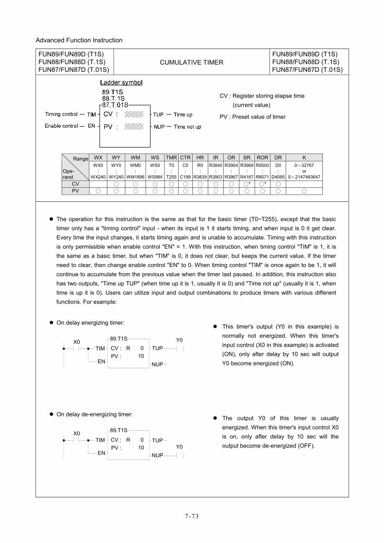
Advanced Function Instruction
7-73
FUN89/FUN89D (T1S) FUN88/FUN88D (T.1S) FUN87/FUN87D (T.01S)
CUMULATIVE TIMER FUN89/FUN89D (T1S) FUN88/FUN88D (T.1S) FUN87/FUN87D (T.01S)
CV : Register storing elapse time (current value)
PV : Preset value of timer
WX WY WM WS TMR CTR HR IR OR SR ROR DR K Range
Ope- rand
WX0 ∣
WX240
WY0 ∣
WY240
WM0 ∣
WM1896
WS0∣
WS984
T0∣
T255
C0∣
C199
R0∣
R3839
R3840∣
R3903
R3904∣
R3967
R3968∣
R4167
R5000∣
R8071
D0 ∣
D4095
0~32767 or
0~2147483647CV ○ ○ ○ ○ ○ ○ ○ ○ ○* ○* ○ PV ○ ○ ○ ○ ○ ○ ○ ○ ○ ○ ○ ○ ○
The operation for this instruction is the same as that for the basic timer (T0~T255), except that the basic timer only has a "timing control" input - when its input is 1 it starts timing, and when input is 0 it get clear. Every time the input changes, it starts timing again and is unable to accumulate. Timing with this instruction is only permissible when enable control "EN" = 1. With this instruction, when timing control "TIM" is 1, it is the same as a basic timer, but when "TIM" is 0, it does not clear, but keeps the current value. If the timer need to clear, then change enable control "EN" to 0. When timing control "TIM" is once again to be 1, it will continue to accumulate from the previous value when the timer last paused. In addition, this instruction also has two outputs, "Time up TUP" (when time up it is 1, usually it is 0) and "Time not up" (usually it is 1, when time is up it is 0). Users can utilize input and output combinations to produce timers with various different functions. For example:
On delay energizing timer:
X0TIM CV :
PV : 10R 0
89.T1S
TUPY0
EN NUP
This timer's output (Y0 in this example) is normally not energized. When this timer's input control (X0 in this example) is activated (ON), only after delay by 10 sec will output Y0 become energized (ON).
On delay de-energizing timer:
X0TIM CV :
PV : 10R 0
89.T1S
Y0NUPEN
TUP
The output Y0 of this timer is usually energized. When this timer's input control X0 is on, only after delay by 10 sec will the output become de-energized (OFF).
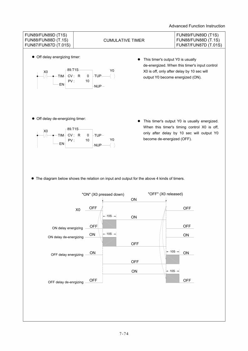
Advanced Function Instruction
7-74
FUN89/FUN89D (T1S) FUN88/FUN88D (T.1S) FUN87/FUN87D (T.01S)
CUMULATIVE TIMER FUN89/FUN89D (T1S) FUN88/FUN88D (T.1S) FUN87/FUN87D (T.01S)
Off delay energizing timer:
X0TIM CV :
PV : 10R 0
89.T1S
TUPY0
EN NUP
This timer's output Y0 is usually de-energized. When this timer's input control X0 is off, only after delay by 10 sec will output Y0 become energized (ON).
Off delay de-energizing timer:
X0TIM CV :
PV : 10R 0
89.T1S
Y0NUPEN
TUP
This timer's output Y0 is usually energized. When this timer's timing control X0 is off, only after delay by 10 sec will output Y0 become de-energized (OFF).
The diagram below shows the relation on input and output for the above 4 kinds of timers.
OFF
OFF
OFF
OFF
OFF
OFF
ON
ON
ON
ON
ON
ON
ON
OFF
OFF
"ON" (X0 pressed down) "OFF" (X0 released)
X0
ON delay energizing
ON delay de-energizing
OFF delay energizing
OFF delay de-enrgizing
10S
10S
10S
10S
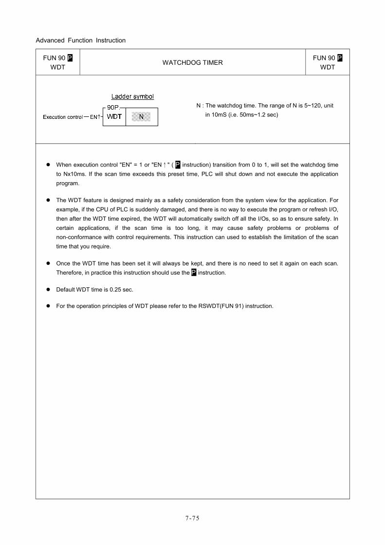
Advanced Function Instruction
7-75
FUN 90 P WDT
WATCHDOG TIMER FUN 90 P
WDT
N : The watchdog time. The range of N is 5~120, unit in 10mS (i.e. 50ms~1.2 sec)
When execution control "EN" = 1 or "EN↑" ( P instruction) transition from 0 to 1, will set the watchdog time to Nx10ms. If the scan time exceeds this preset time, PLC will shut down and not execute the application program.
The WDT feature is designed mainly as a safety consideration from the system view for the application. For example, if the CPU of PLC is suddenly damaged, and there is no way to execute the program or refresh I/O, then after the WDT time expired, the WDT will automatically switch off all the I/Os, so as to ensure safety. In certain applications, if the scan time is too long, it may cause safety problems or problems of non-conformance with control requirements. This instruction can used to establish the limitation of the scan time that you require.
Once the WDT time has been set it will always be kept, and there is no need to set it again on each scan. Therefore, in practice this instruction should use the P instruction.
Default WDT time is 0.25 sec.
For the operation principles of WDT please refer to the RSWDT(FUN 91) instruction.
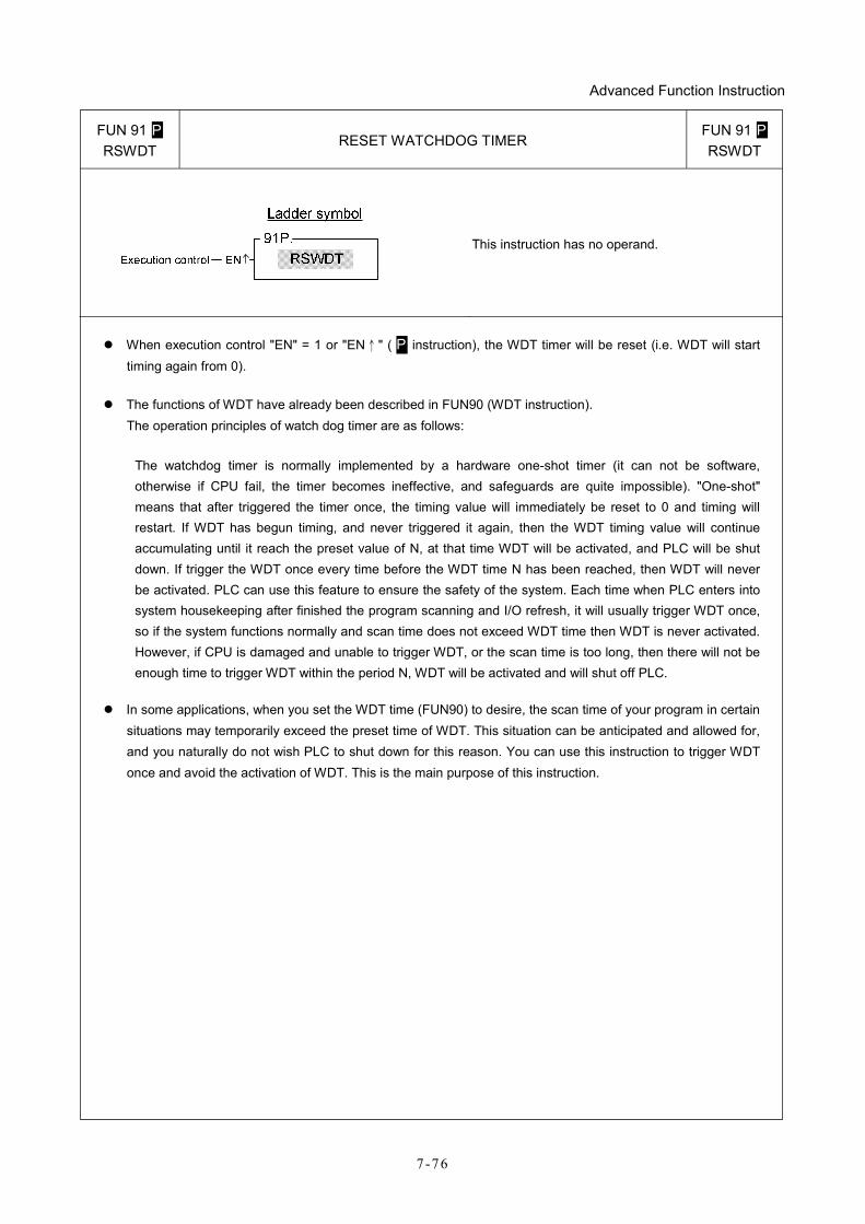
Advanced Function Instruction
7 -76
FUN 91 P RSWDT
RESET WATCHDOG TIMER FUN 91 P RSWDT
This instruction has no operand.
When execution control "EN" = 1 or "EN↑" ( P instruction), the WDT timer will be reset (i.e. WDT will start timing again from 0).
The functions of WDT have already been described in FUN90 (WDT instruction). The operation principles of watch dog timer are as follows:
The watchdog timer is normally implemented by a hardware one-shot timer (it can not be software, otherwise if CPU fail, the timer becomes ineffective, and safeguards are quite impossible). "One-shot" means that after triggered the timer once, the timing value will immediately be reset to 0 and timing will restart. If WDT has begun timing, and never triggered it again, then the WDT timing value will continue accumulating until it reach the preset value of N, at that time WDT will be activated, and PLC will be shut down. If trigger the WDT once every time before the WDT time N has been reached, then WDT will never be activated. PLC can use this feature to ensure the safety of the system. Each time when PLC enters into system housekeeping after finished the program scanning and I/O refresh, it will usually trigger WDT once, so if the system functions normally and scan time does not exceed WDT time then WDT is never activated. However, if CPU is damaged and unable to trigger WDT, or the scan time is too long, then there will not be enough time to trigger WDT within the period N, WDT will be activated and will shut off PLC.
In some applications, when you set the WDT time (FUN90) to desire, the scan time of your program in certain situations may temporarily exceed the preset time of WDT. This situation can be anticipated and allowed for, and you naturally do not wish PLC to shut down for this reason. You can use this instruction to trigger WDT once and avoid the activation of WDT. This is the main purpose of this instruction.
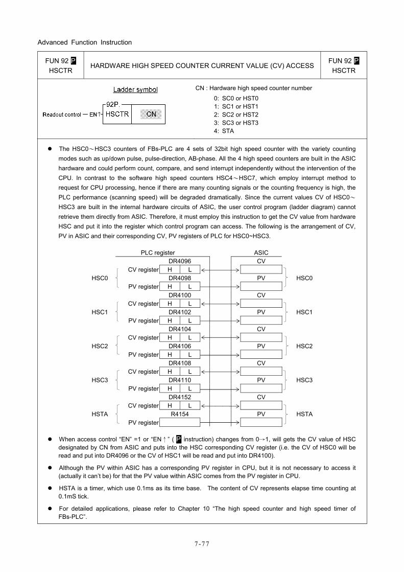
Advanced Function Instruction
7 -77
FUN 92 P HSCTR
HARDWARE HIGH SPEED COUNTER CURRENT VALUE (CV) ACCESS FUN 92 P HSCTR
CN : Hardware high speed counter number
0: SC0 or HST0 1: SC1 or HST1 2: SC2 or HST2 3: SC3 or HST3 4: STA
The HSC0~HSC3 counters of FBs-PLC are 4 sets of 32bit high speed counter with the variety counting modes such as up/down pulse, pulse-direction, AB-phase. All the 4 high speed counters are built in the ASIC hardware and could perform count, compare, and send interrupt independently without the intervention of the CPU. In contrast to the software high speed counters HSC4~HSC7, which employ interrupt method to request for CPU processing, hence if there are many counting signals or the counting frequency is high, the PLC performance (scanning speed) will be degraded dramatically. Since the current values CV of HSC0~HSC3 are built in the internal hardware circuits of ASIC, the user control program (ladder diagram) cannot retrieve them directly from ASIC. Therefore, it must employ this instruction to get the CV value from hardware HSC and put it into the register which control program can access. The following is the arrangement of CV, PV in ASIC and their corresponding CV, PV registers of PLC for HSC0~HSC3.
PLC register ASIC DR4096 CV CV register H L
HSC0 DR4098 PV HSC0 PV register H L DR4100 CV CV register H L
HSC1 DR4102 PV HSC1 PV register H L DR4104 CV CV register H L
HSC2 DR4106 PV HSC2 PV register H L DR4108 CV CV register H L
HSC3 DR4110 PV HSC3 PV register H L DR4152 CV CV register H L
HSTA R4154 PV HSTA PV register
When access control “EN” =1 or “EN↑” ( P instruction) changes from 0→1, will gets the CV value of HSC designated by CN from ASIC and puts into the HSC corresponding CV register (i.e. the CV of HSC0 will be read and put into DR4096 or the CV of HSC1 will be read and put into DR4100).
Although the PV within ASIC has a corresponding PV register in CPU, but it is not necessary to access it (actually it can’t be) for that the PV value within ASIC comes from the PV register in CPU.
HSTA is a timer, which use 0.1ms as its time base. The content of CV represents elapse time counting at 0.1mS tick.
For detailed applications, please refer to Chapter 10 “The high speed counter and high speed timer of FBs-PLC”.
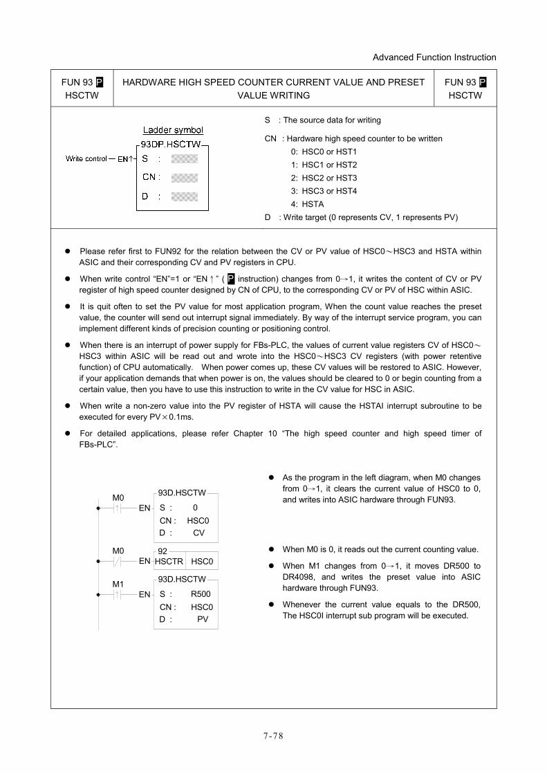
Advanced Function Instruction
7 -78
FUN 93 P HSCTW
HARDWARE HIGH SPEED COUNTER CURRENT VALUE AND PRESET VALUE WRITING
FUN 93 P HSCTW
S : The source data for writing
CN : Hardware high speed counter to be written 0: HSC0 or HST1 1: HSC1 or HST2 2: HSC2 or HST3 3: HSC3 or HST4 4: HSTA
D : Write target (0 represents CV, 1 represents PV)
Please refer first to FUN92 for the relation between the CV or PV value of HSC0~HSC3 and HSTA within ASIC and their corresponding CV and PV registers in CPU.
When write control “EN”=1 or “EN↑” ( P instruction) changes from 0→1, it writes the content of CV or PV register of high speed counter designed by CN of CPU, to the corresponding CV or PV of HSC within ASIC.
It is quit often to set the PV value for most application program, When the count value reaches the preset value, the counter will send out interrupt signal immediately. By way of the interrupt service program, you can implement different kinds of precision counting or positioning control.
When there is an interrupt of power supply for FBs-PLC, the values of current value registers CV of HSC0~HSC3 within ASIC will be read out and wrote into the HSC0~HSC3 CV registers (with power retentive function) of CPU automatically. When power comes up, these CV values will be restored to ASIC. However, if your application demands that when power is on, the values should be cleared to 0 or begin counting from a certain value, then you have to use this instruction to write in the CV value for HSC in ASIC.
When write a non-zero value into the PV register of HSTA will cause the HSTAI interrupt subroutine to be executed for every PV×0.1ms.
For detailed applications, please refer Chapter 10 “The high speed counter and high speed timer of FBs-PLC”.
EN S :
D :
EN
EN
D :
S :M1
M0
M0 93D.HSCTW
92
93D.HSCTW
CN : HSC0CV
0
HSC0HSCTR
CN :R500HSC0
PV
As the program in the left diagram, when M0 changes from 0→1, it clears the current value of HSC0 to 0, and writes into ASIC hardware through FUN93.
When M0 is 0, it reads out the current counting value.
When M1 changes from 0→1, it moves DR500 to DR4098, and writes the preset value into ASIC hardware through FUN93.
Whenever the current value equals to the DR500, The HSC0I interrupt sub program will be executed.
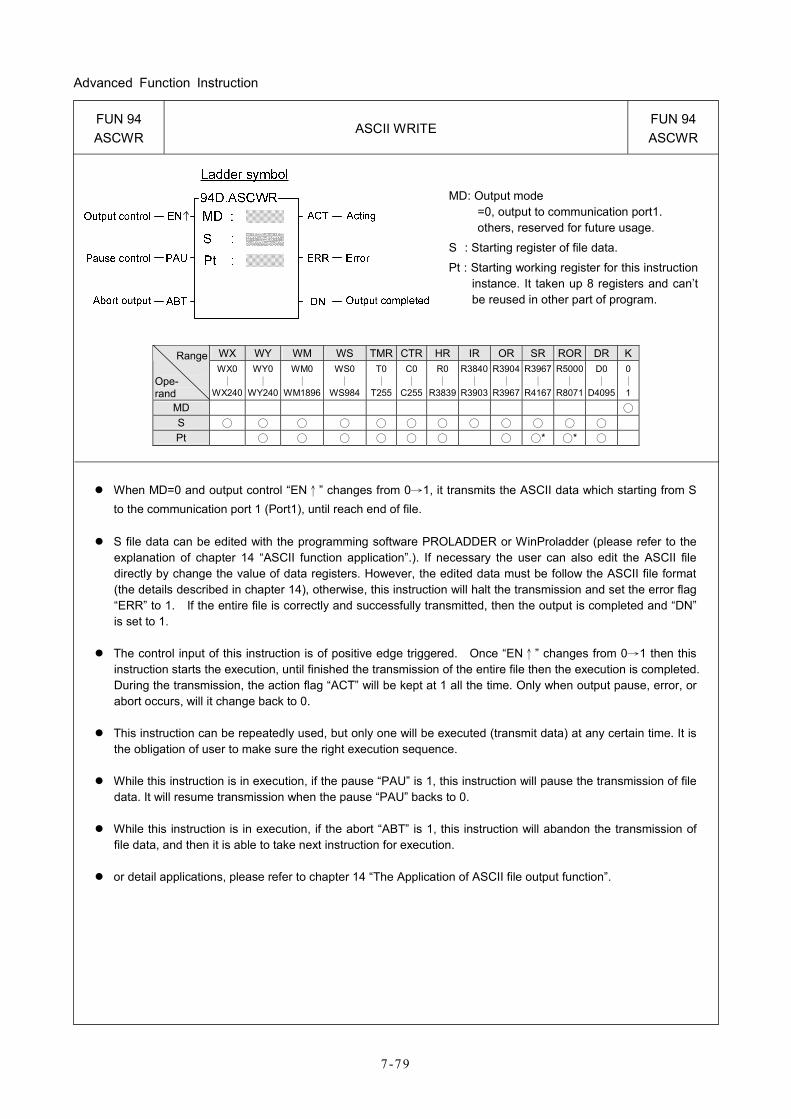
Advanced Function Instruction
7 -79
FUN 94 ASCWR
ASCII WRITE FUN 94 ASCWR
MD: Output mode =0, output to communication port1. others, reserved for future usage.
S : Starting register of file data.
Pt : Starting working register for this instruction instance. It taken up 8 registers and can’t be reused in other part of program.
WX WY WM WS TMR CTR HR IR OR SR ROR DR K Range
Ope- rand
WX0∣
WX240
WY0 ∣
WY240
WM0 ∣
WM1896
WS0 ∣
WS984
T0∣
T255
C0∣
C255
R0∣
R3839
R3840∣
R3903
R3904∣
R3967
R3967∣
R4167
R5000 ∣
R8071
D0 ∣
D4095
0 ∣ 1
MD ○ S ○ ○ ○ ○ ○ ○ ○ ○ ○ ○ ○ ○ Pt ○ ○ ○ ○ ○ ○ ○ ○* ○* ○
When MD=0 and output control “EN↑” changes from 0→1, it transmits the ASCII data which starting from S to the communication port 1 (Port1), until reach end of file.
S file data can be edited with the programming software PROLADDER or WinProladder (please refer to the explanation of chapter 14 “ASCII function application”.). If necessary the user can also edit the ASCII file directly by change the value of data registers. However, the edited data must be follow the ASCII file format (the details described in chapter 14), otherwise, this instruction will halt the transmission and set the error flag “ERR” to 1. If the entire file is correctly and successfully transmitted, then the output is completed and “DN” is set to 1.
The control input of this instruction is of positive edge triggered. Once “EN↑” changes from 0→1 then this instruction starts the execution, until finished the transmission of the entire file then the execution is completed. During the transmission, the action flag “ACT” will be kept at 1 all the time. Only when output pause, error, or abort occurs, will it change back to 0.
This instruction can be repeatedly used, but only one will be executed (transmit data) at any certain time. It is the obligation of user to make sure the right execution sequence.
While this instruction is in execution, if the pause “PAU” is 1, this instruction will pause the transmission of file data. It will resume transmission when the pause “PAU” backs to 0.
While this instruction is in execution, if the abort “ABT” is 1, this instruction will abandon the transmission of file data, and then it is able to take next instruction for execution.
or detail applications, please refer to chapter 14 “The Application of ASCII file output function”.

Advanced Function Instruction
7 -80
FUN 94 ASCWR
ASCII WRITE FUN 94 ASCWR
Interface signals: M1927: This signal is control by CPU, it is applied in ASCWR MD:0
: ON, it represents that the RTS (connect to the CTS of PLC) of the printer is “False”. I.e. the printer is not ready or abnormal. : OFF, it represents that the RTS of the Printer is “True”; Printer is Ready.
Note: Using the M1927 associates with timer can detect if the printer is abnormal or not.
R4158: The setting of communication parameters (refer to section 11.7.2)
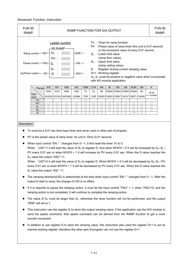
Advanced Function Instruction
7 -81
FUN 95 RAMP
RAMP FUNCTION FOR D/A OUTPUT FUN 95 RAMP
Tn :
S :
ENRamp control
Ladder symbol
95.RAMP
PV :
ERR
S :
ASL
D : ASU
Pause control PAU
Up/Down output U/D
L
U
Tn : Timer for ramp function PV : Preset value of ramp timer (the unit is 0.01 second)
or the increment value of every 0.01 second SL : Lower limit value
(ramp floor value). SU : Upper limit value
(ramp ceiling value). D : Register storing current ramping value. D+1 : Working register SU, SL could be positive or negative value when incorporate with AO module application.
WX WY WM WS TMR CTR HR IR OR SR ROR DR K Range
Ope- rand
WX0 ∣
WX240
WY0 ∣
WY240
WM0 ∣
WM1896
WS0 ∣
WS984
T0 ∣
T255
C0 ∣
C255
R0 ∣
R3839
R3840∣
R3903
R3904∣
R3967
R3968∣
R4167
R5000 ∣
R8071
D0 ∣
D4095
16-bit +/- number
Tn ○ PV ○ ○ ○ ○ ○ ○ ○ ○ ○ ○ ○ ○ ○ SL ○ ○ ○ ○ ○ ○ ○ ○ ○ ○ ○ ○ ○ SU ○ ○ ○ ○ ○ ○ ○ ○ ○ ○ ○ ○ ○ D ○ ○ ○ ○ ○ ○ ○ ○ ○* ○
Description
Tn must be a 0.01 sec time base timer and never used in other part of program.
PV is the preset value of ramp timer. Its unit is 10ms (0.01 second).
When input control “EN↑” changes from 0→1, it first reset the timer Tn to 0. When “U/D”=1 it will load the value of SL to register D. And when M1974 = 0 it will be increased by SU−SL / PV every 0.01 sec or when M1974 = 1 it will increase by PV every 0.01 sec. When the D value reaches the SU value the output “ASU” =1. When “U/D”=0 it will load the value of SU to register D. When M1974 = 0 it will be decreased by SU−SL / PV every 0.01 sec or when M1974 = 1 it will be decreased by PV every 0.01 sec. When the D value reaches the SL value the output “ASL” =1.
The ramping direction(U/D) is determined at the time when input control “EN↑” changes from 0→1. After the output D start to ramp, the change of U/D is no effect.
If it is required to pause the ramping action, it must let the input control “PAU” = 1; when “PAU”=0, and the ramping action is not completed, it will continue to complete the ramping action.
The value of SU must be larger than SL, otherwise the ramp function will not be performed, and the output “ERR” will set to 1.
This instruction use the register D to store the output ramping value; if the application use the D/A module to send the speed command, then speed command can be derived from the RAMP function to get a more smooth movement.
In addition to use register D to store the ramping value, this instruction also used the register D+1 to act as internal working register; therefore the other part of program can not use the register D+1.
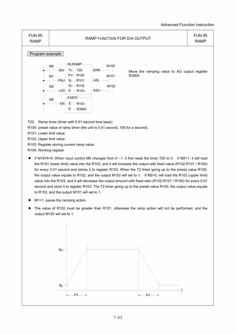
Advanced Function Instruction
7 -82
FUN 95 RAMP
RAMP FUNCTION FOR D/A OUTPUT FUN 95 RAMP
Program example
M0EN Tn : T20 ERR
M100
PV : R100SL :
D :SU :
M1PAU
M2U/D
ASLM101
ASU
R101R102R103
M102
M0EN
8.MOV
D : R3904
S : R103
95.RAMP
Move the ramping value to AO output register R3904
T20: Ramp timer (timer with 0.01 second time base) R100: preset value of ramp timer (the unit is 0.01 second, 100 for a second). R101: Lower limit value. R102: Upper limit value. R103: Register storing current ramp value. R104: Working register
If M1974=0, When input control M0 changes from 0→1, it first reset the timer T20 to 0. If M2=1, it will load the R101 (lower limit) value into the R103, and it will increase the output with fixed value (R102-R101 / R100) for every 0.01 second and stores it to register R103. When the T2 timer going up to the preset value R100, the output value equals to R102, and the output M102 will set to 1. If M2=0, will load the R102 (upper limit) value into the R103, and it will decrease the output amount with fixed ratio (R102-R101 / R100) for every 0.01 second and store it to register R103. The T2 timer going up to the preset value R100, the output value equals to R102, and the output M101 will set to 1.
M1=1, pause the ramping action.
The value of R102 must be greater than R101, otherwise the ramp action will not be performed, and the output M100 will set to 1.
SU
SL
PV PVt
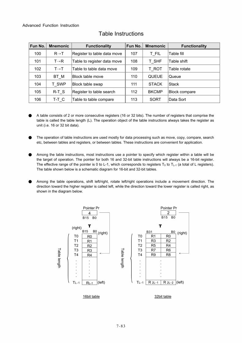
Advanced Function Instruction
7-83
Table Instructions
Fun No. Mnemonic Functionality Fun No. Mnemonic Functionality
100 R→T Register to table data move 107 T_FIL Table fill
101 T→R Table to register data move 108 T_SHF Table shift
102 T→T Table to table data move 109 T_ROT Table rotate
103 BT_M Block table move 110 QUEUE Queue
104 T_SWP Block table swap 111 STACK Stack
105 R-T_S Register to table search 112 BKCMP Block compare
106 T-T_C Table to table compare 113 SORT Data Sort
● A table consists of 2 or more consecutive registers (16 or 32 bits). The number of registers that comprise the table is called the table length (L). The operation object of the table instructions always takes the register as unit (i.e. 16 or 32 bit data).
● The operation of table instructions are used mostly for data processing such as move, copy, compare, search etc, between tables and registers, or between tables. These instructions are convenient for application.
● Among the table instructions, most instructions use a pointer to specify which register within a table will be the target of operation. The pointer for both 16 and 32-bit table instructions will always be a 16-bit register. The effective range of the pointer is 0 to L-1, which corresponds to registers T0 to TL-1 (a total of L registers). The table shown below is a schematic diagram for 16-bit and 32-bit tables.
● Among the table operations, shift left/right, rotate left/right operations include a movement direction. The direction toward the higher register is called left, while the direction toward the lower register is called right, as shown in the diagram below.
Pointer Pr Pointer Pr 4 2 B15 B0 B15 B0
(right) B15 B0 B31 B0
T0 R0 T0 R1 R0 T1 R1 T1 R3 R2 T2 R2 T2 R5 R4 T3 R3 T3 R7 R6 T4 R4
──┐││││
(right)│││││
←─┘ T4 R9 R8
──┐ │ │ │ │
(right)│ │ │ │ │
←─┘
......
......
......
......
TL−1 RL-1 (left) TL−1 R 2L−1 R 2L−2 (left)
Table length
{
16bit table
Table length
{
32bit table
T T
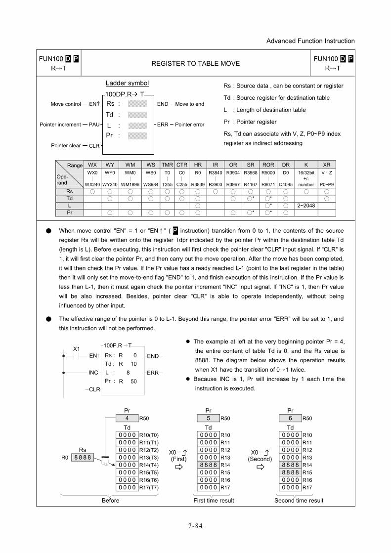
Advanced Function Instruction
7-84
FUN100 D P R→T
REGISTER TO TABLE MOVE FUN100 D P
R→T
Rs :
L :
ENMove control
Ladder symbol
100DP.R T
Td :
END Move to end
ERR Pointer errorPointer increment PAU
Pointer clear CLR
Pr :
Rs : Source data , can be constant or register
Td : Source register for destination table
L : Length of destination table
Pr : Pointer register
Rs, Td can associate with V, Z, P0~P9 index register as indirect addressing
WX WY WM WS TMR CTR HR IR OR SR ROR DR K XRRange
Ope- rand
WX0 ∣
WX240
WY0∣
WY240
WM0 ∣
WM1896
WS0 ∣
WS984
T0∣
T255
C0∣
C255
R0 ∣
R3839
R3840∣
R3903
R3904∣
R3967
R3968∣
R4167
R5000∣
R8071
D0 ∣
D4095
16/32bit +/-
number
V、Z
P0~P9Rs ○ ○ ○ ○ ○ ○ ○ ○ ○ ○ ○ ○ ○ ○ Td ○ ○ ○ ○ ○ ○ ○ ○* ○* ○ ○ L ○ ○* ○ 2~2048 Pr ○ ○ ○ ○ ○ ○ ○ ○* ○* ○
● When move control "EN" = 1 or "EN↑" ( P instruction) transition from 0 to 1, the contents of the source register Rs will be written onto the register Tdpr indicated by the pointer Pr within the destination table Td (length is L). Before executing, this instruction will first check the pointer clear "CLR" input signal. If "CLR" is 1, it will first clear the pointer Pr, and then carry out the move operation. After the move has been completed, it will then check the Pr value. If the Pr value has already reached L-1 (point to the last register in the table) then it will only set the move-to-end flag "END" to 1, and finish execution of this instruction. If the Pr value is less than L-1, then it must again check the pointer increment "INC" input signal. If "INC" is 1, then Pr value will be also increased. Besides, pointer clear "CLR" is able to operate independently, without being influenced by other input.
● The effective range of the pointer is 0 to L-1. Beyond this range, the pointer error "ERR" will be set to 1, and this instruction will not be performed.
X1EN RS : R 0
100P.R T
Td : R 10L :Pr :
INC
CLR
8R 50
ERR
END
The example at left at the very beginning pointer Pr = 4, the entire content of table Td is 0, and the Rs value is 8888. The diagram below shows the operation results when X1 have the transition of 0→1 twice.
Because INC is 1, Pr will increase by 1 each time the instruction is executed.
Pr Pr Pr 4 R50 5 R50 6 R50
Td Td Td 0 0 0 0 R10(T0) 0 0 0 0 R10 0 0 0 0 R10 0 0 0 0 R11(T1) 0 0 0 0 R11 0 0 0 0 R11 Rs 0 0 0 0 R12(T2) 0 0 0 0 R12 0 0 0 0 R12
R0 8 8 8 8 0 0 0 0 R13(T3) 0 0 0 0 R13 0 0 0 0 R13 0 0 0 0 R14(T4) 8 8 8 8 R14 8 8 8 8 R14 0 0 0 0 R15(T5) 0 0 0 0 R15 8 8 8 8 R15 0 0 0 0 R16(T6) 0 0 0 0 R16 0 0 0 0 R16 0 0 0 0 R17(T7)
X0= (First)
0 0 0 0 R17
X0= (Second)
0 0 0 0 R17
Before First time result Second time result
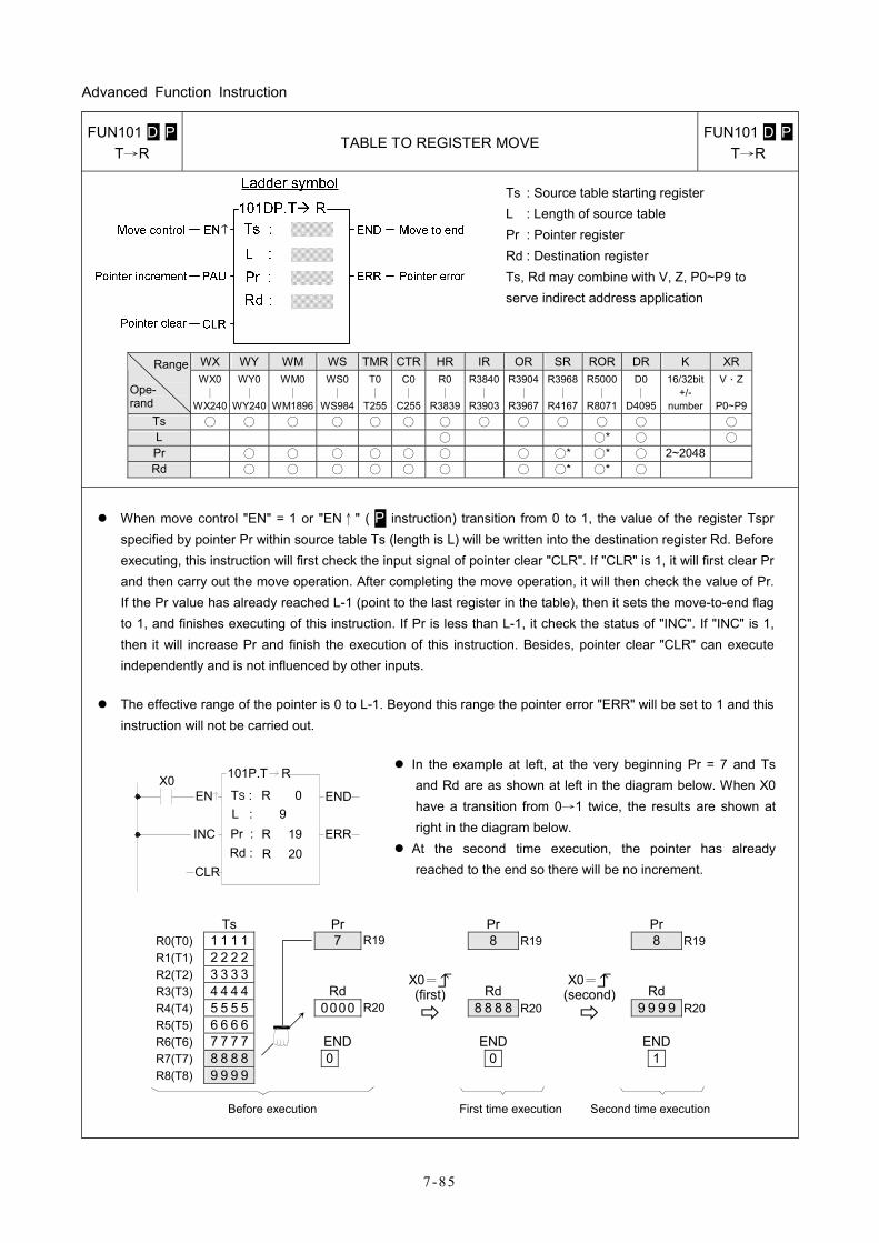
Advanced Function Instruction
7 -85
FUN101 D P T→R
TABLE TO REGISTER MOVE FUN101 D P
T→R
Ts : Source table starting register L : Length of source table Pr : Pointer register Rd : Destination register Ts, Rd may combine with V, Z, P0~P9 to serve indirect address application
WX WY WM WS TMR CTR HR IR OR SR ROR DR K XRRange
Ope- rand
WX0 ∣
WX240
WY0∣
WY240
WM0 ∣
WM1896
WS0 ∣
WS984
T0∣
T255
C0∣
C255
R0 ∣
R3839
R3840∣
R3903
R3904∣
R3967
R3968∣
R4167
R5000∣
R8071
D0 ∣
D4095
16/32bit +/-
number
V、Z
P0~P9Ts ○ ○ ○ ○ ○ ○ ○ ○ ○ ○ ○ ○ ○ L ○ ○* ○ ○ Pr ○ ○ ○ ○ ○ ○ ○ ○* ○* ○ 2~2048 Rd ○ ○ ○ ○ ○ ○ ○ ○* ○* ○
When move control "EN" = 1 or "EN↑" ( P instruction) transition from 0 to 1, the value of the register Tspr specified by pointer Pr within source table Ts (length is L) will be written into the destination register Rd. Before executing, this instruction will first check the input signal of pointer clear "CLR". If "CLR" is 1, it will first clear Pr and then carry out the move operation. After completing the move operation, it will then check the value of Pr. If the Pr value has already reached L-1 (point to the last register in the table), then it sets the move-to-end flag to 1, and finishes executing of this instruction. If Pr is less than L-1, it check the status of "INC". If "INC" is 1, then it will increase Pr and finish the execution of this instruction. Besides, pointer clear "CLR" can execute independently and is not influenced by other inputs.
The effective range of the pointer is 0 to L-1. Beyond this range the pointer error "ERR" will be set to 1 and this instruction will not be carried out.
X0EN TS : R 0
101P.T R
Rd :R 19
L :Pr :INC
CLR
9
R 20ERR
END
In the example at left, at the very beginning Pr = 7 and Ts and Rd are as shown at left in the diagram below. When X0 have a transition from 0→1 twice, the results are shown at right in the diagram below.
At the second time execution, the pointer has already reached to the end so there will be no increment.
Ts Pr Pr Pr R0(T0) 1 1 1 1 7 R19 8 R19 8 R19 R1(T1) 2 2 2 2 R2(T2) 3 3 3 3 R3(T3) 4 4 4 4 Rd Rd Rd R4(T4) 5 5 5 5 0000 R20 8 8 8 8 R20 9 9 9 9 R20 R5(T5) 6 6 6 6 R6(T6) 7 7 7 7 END END END R7(T7) 8 8 8 8 0
X0= (first)
0
X0= (second)
1 R8(T8) 9 9 9 9
Before execution First time execution Second time execution
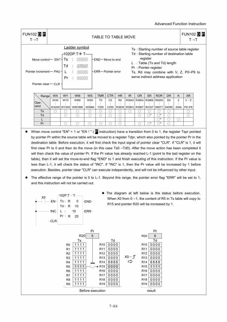
Advanced Function Instruction
7-86
FUN102 D P T→T
TABLE TO TABLE MOVE FUN102 D P
T→T
Ts :ENMove control
Ladder symbol
102DP.T T
Td :
END Move to end
ERR Pointer errorPointer increment PAU
Pointer clear CLR
L :Pr :
Ts : Starting number of source table register Td : Starting number of destination table
register L : Table (Ts and Td) length Pr : Pointer register Ts, Rd may combine with V, Z, P0~P9 to serve indirect address application
WX WY WM WS TMR CTR HR IR OR SR ROR DR K XRRange
Ope- rand
WX0 ∣
WX240
WY0∣
WY240
WM0 ∣
WM1896
WS0 ∣
WS984
T0 ∣
T255
C0 ∣
C255
R0 ∣
R3839
R3840∣
R3903
R3904∣
R3967
R3968∣
R4167
R5000 ∣
R8071
D0 ∣
D4095
2 ∣
2048
V、Z
P0~P9Ts ○ ○ ○ ○ ○ ○ ○ ○ ○ ○ ○ ○ ○
Td ○ ○ ○ ○ ○ ○ ○ ○* ○* ○ ○
L ○ ○* ○ ○ Pr ○ ○ ○ ○ ○ ○ ○ ○* ○* ○
When move control "EN" = 1 or "EN↑" ( P instruction) have a transition from 0 to 1, the register Tspr pointed
by pointer Pr within the source table will be moved to a register Tdpr, which also pointed by the pointer Pr in the destination table. Before execution, it will first check the input signal of pointer clear "CLR". If "CLR" is 1, it will first clear Pr to 0 and then do the move (in this case Ts0→Td0). After the move action has been completed it will then check the value of pointer Pr. If the Pr value has already reached L-1 (point to the last register on the table), then it will set the move-to-end flag "END" to 1 and finish executing of this instruction. If the Pr value is less than L-1, it will check the status of "INC". If "INC" is 1, then the Pr value will be increased by 1 before execution. Besides, pointer clear "CLR" can execute independently, and will not be influenced by other input.
The effective range of the pointer is 0 to L-1. Beyond this range, the pointer error flag "ERR" will be set to 1, and this instruction will not be carried out.
X0EN TS : R 0
102P.T T
ENDTd : R 10L :Pr :
INC ERR10R 20
CLR
The diagram at left below is the status before execution. When X0 from 0→1, the content of R5 in Ts table will copy to R15 and pointer R20 will be increased by 1.
Pr Pr R20 5 R20 6 Ts Td Td
R0 1 1 1 1 R10 0 0 0 0 R10 0 0 0 0R1 1 1 1 1 R11 0 0 0 0 R11 0 0 0 0R2 1 1 1 1 R12 0 0 0 0 R12 0 0 0 0R3 1 1 1 1 R13 0 0 0 0 R13 0 0 0 0R4 1 1 1 1 R14 8 8 8 8 R14 8 8 8 8R5 1 1 1 1 R15 0 0 0 0 R15 1 1 1 1R6 1 1 1 1 R16 0 0 0 0 R16 0 0 0 0R7 1 1 1 1 R17 0 0 0 0
X0=
R17 0 0 0 0R8 1 1 1 1 R18 0 0 0 0 R18 0 0 0 0R9 1 1 1 1 R19 0 0 0 0 R19 0 0 0 0
Before execution result
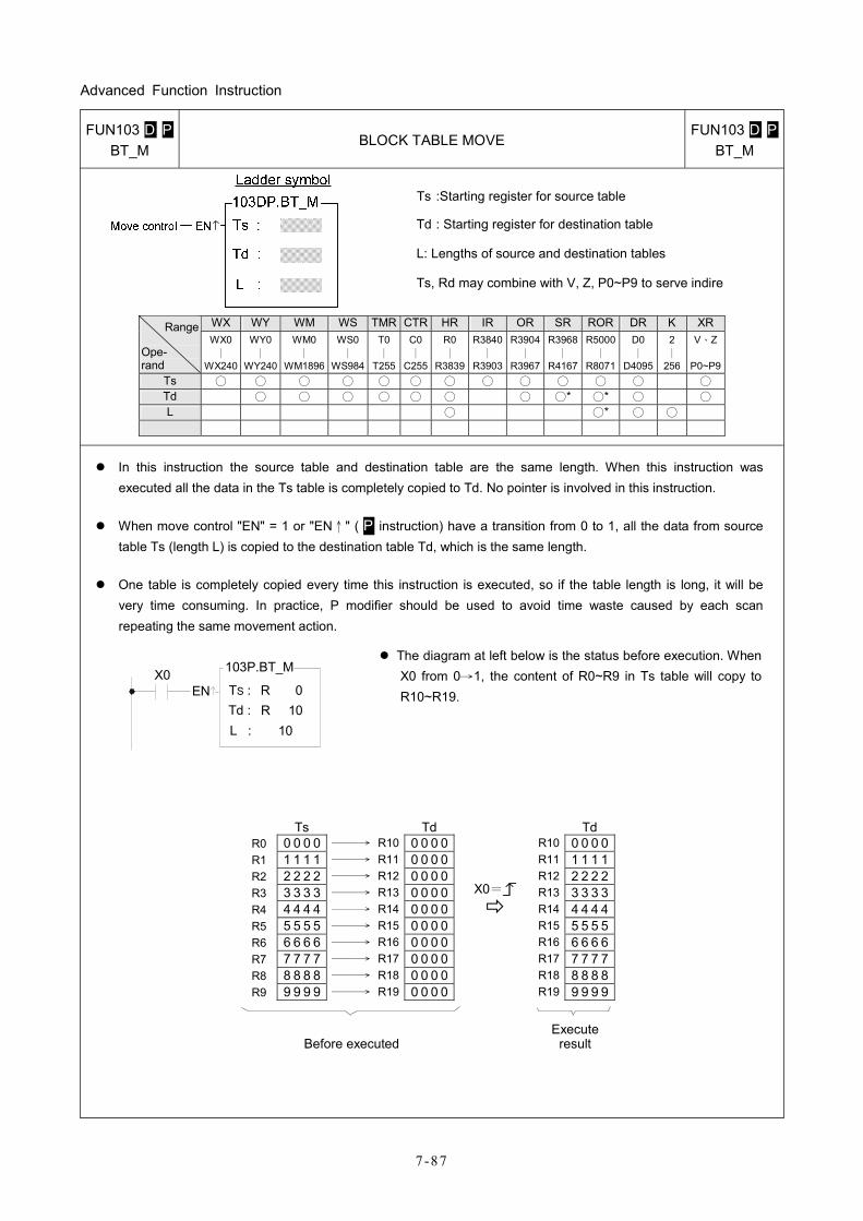
Advanced Function Instruction
7 -87
FUN103 D P BT_M
BLOCK TABLE MOVE FUN103 D P
BT_M
Ts :Starting register for source table
Td : Starting register for destination table
L: Lengths of source and destination tables
Ts, Rd may combine with V, Z, P0~P9 to serve indire
WX WY WM WS TMR CTR HR IR OR SR ROR DR K XRRange
Ope- rand
WX0 ∣
WX240
WY0 ∣
WY240
WM0 ∣
WM1896
WS0∣
WS984
T0∣
T255
C0∣
C255
R0 ∣
R3839
R3840∣
R3903
R3904∣
R3967
R3968∣
R4167
R5000 ∣
R8071
D0 ∣
D4095
2 ∣
256
V、Z
P0~P9Ts ○ ○ ○ ○ ○ ○ ○ ○ ○ ○ ○ ○ ○ Td ○ ○ ○ ○ ○ ○ ○ ○* ○* ○ ○ L ○ ○* ○ ○
In this instruction the source table and destination table are the same length. When this instruction was executed all the data in the Ts table is completely copied to Td. No pointer is involved in this instruction.
When move control "EN" = 1 or "EN↑" ( P instruction) have a transition from 0 to 1, all the data from source table Ts (length L) is copied to the destination table Td, which is the same length.
One table is completely copied every time this instruction is executed, so if the table length is long, it will be very time consuming. In practice, P modifier should be used to avoid time waste caused by each scan repeating the same movement action.
X0EN TS : R 0
Td : R 10L : 10
103P.BT_M
The diagram at left below is the status before execution. When X0 from 0→1, the content of R0~R9 in Ts table will copy to R10~R19.
Ts Td Td R0 0 0 0 0 ──→ R10 0 0 0 0 R10 0 0 0 0R1 1 1 1 1 ──→ R11 0 0 0 0 R11 1 1 1 1R2 2 2 2 2 ──→ R12 0 0 0 0 R12 2 2 2 2R3 3 3 3 3 ──→ R13 0 0 0 0 R13 3 3 3 3R4 4 4 4 4 ──→ R14 0 0 0 0 R14 4 4 4 4R5 5 5 5 5 ──→ R15 0 0 0 0 R15 5 5 5 5R6 6 6 6 6 ──→ R16 0 0 0 0 R16 6 6 6 6R7 7 7 7 7 ──→ R17 0 0 0 0
X0=
R17 7 7 7 7R8 8 8 8 8 ──→ R18 0 0 0 0 R18 8 8 8 8R9 9 9 9 9 ──→ R19 0 0 0 0 R19 9 9 9 9
Before executed Execute
result
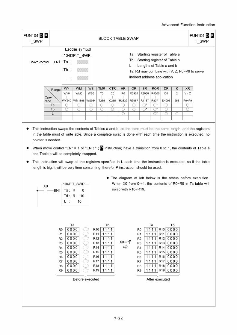
Advanced Function Instruction
7-88
FUN104 D P T_SWP
BLOCK TABLE SWAP FUN104 D P
T_SWP
Ta : Starting register of Table a Tb : Starting register of Table b L : Lengths of Table a and b Ts, Rd may combine with V, Z, P0~P9 to serve indirect address application
WY WM WS TMR CTR HR OR SR ROR DR K XR Range
Ope- rand
WY0∣
WY240
WM0 ∣
WM1896
WS0 ∣
WS984
T0 ∣
T255
C0 ∣
C255
R0 ∣
R3839
R3904∣
R3967
R3968∣
R4167
R5000∣
R8071
D0 ∣
D4095
2 ∣
256
V、Z
P0~P9 Ta ○ ○ ○ ○ ○ ○ ○ ○* ○* ○ ○ Tb ○ ○ ○ ○ ○ ○ ○ ○* ○* ○ ○ L ○ ○* ○ ○
This instruction swaps the contents of Tables a and b, so the table must be the same length, and the registers in the table must of write able. Since a complete swap is done with each time the instruction is executed, no pointer is needed.
When move control "EN" = 1 or "EN↑" ( P instruction) have a transition from 0 to 1, the contents of Table a and Table b will be completely swapped.
This instruction will swap all the registers specified in L each time the instruction is executed, so if the table length is big, it will be very time consuming, therefor P instruction should be used.
X0EN TS : R 0
Td : R 10L : 10
104P.T_SWP
The diagram at left below is the status before execution. When X0 from 0→1, the contents of R0~R9 in Ts table will swap with R10~R19.
Ta Tb Ta Tb R0 0 0 0 0 R10 1 1 1 1 R0 1 1 1 1 R10 0 0 0 0 R1 0 0 0 0 R11 1 1 1 1 R1 1 1 1 1 R11 0 0 0 0 R2 0 0 0 0 R12 1 1 1 1 R2 1 1 1 1 R12 0 0 0 0 R3 0 0 0 0 R13 1 1 1 1 R3 1 1 1 1 R13 0 0 0 0 R4 0 0 0 0 R14 1 1 1 1 R4 1 1 1 1 R14 0 0 0 0 R5 0 0 0 0 R15 1 1 1 1 R5 1 1 1 1 R15 0 0 0 0 R6 0 0 0 0 R16 1 1 1 1 R6 1 1 1 1 R16 0 0 0 0 R7 0 0 0 0 R17 1 1 1 1
X0=
R7 1 1 1 1 R17 0 0 0 0 R8 0 0 0 0 R18 1 1 1 1 R8 1 1 1 1 R18 0 0 0 0 R9 0 0 0 0 R19 1 1 1 1 R9 1 1 1 1 R19 0 0 0 0
Before executed After executed
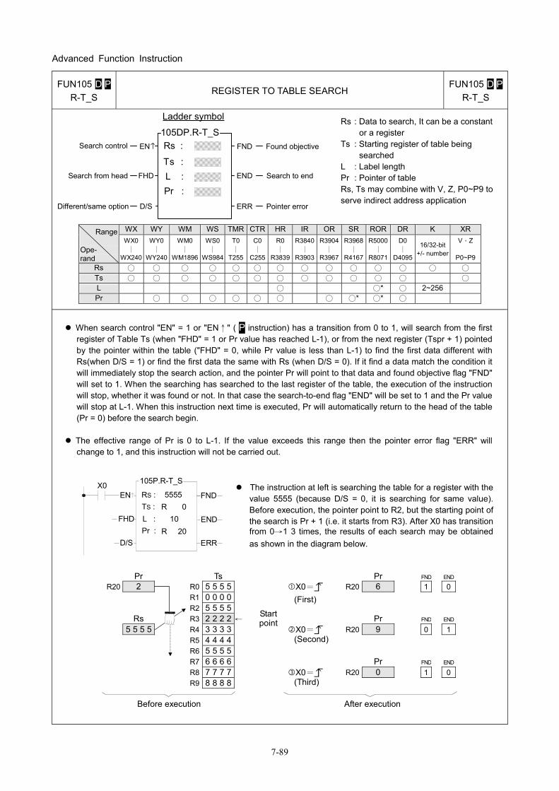
Advanced Function Instruction
7-89
FUN105 D P R-T_S
REGISTER TO TABLE SEARCH FUN105 D P
R-T_S
Rs :ENSearch control
Ladder symbol
105DP.R-T_S
Ts :
FND Found objective
END Search to endSearch from head FHD
Different/same option D/S
L :Pr :
ERR Pointer error
Rs : Data to search, It can be a constant or a register
Ts : Starting register of table being searched
L : Label length Pr : Pointer of table Rs, Ts may combine with V, Z, P0~P9 to serve indirect address application
WX WY WM WS TMR CTR HR IR OR SR ROR DR K XR Range
Ope- rand
WX0 ∣
WX240
WY0 ∣
WY240
WM0 ∣
WM1896
WS0 ∣
WS984
T0 ∣
T255
C0∣
C255
R0 ∣
R3839
R3840∣
R3903
R3904∣
R3967
R3968∣
R4167
R5000∣
R8071
D0 ∣
D4095
16/32-bit +/- number
V、Z
P0~P9Rs ○ ○ ○ ○ ○ ○ ○ ○ ○ ○ ○ ○ ○ ○ Ts ○ ○ ○ ○ ○ ○ ○ ○ ○ ○ ○ ○ ○ L ○ ○* ○ 2~256 Pr ○ ○ ○ ○ ○ ○ ○ ○* ○* ○
When search control "EN" = 1 or "EN↑" ( P instruction) has a transition from 0 to 1, will search from the first register of Table Ts (when "FHD" = 1 or Pr value has reached L-1), or from the next register (Tspr + 1) pointed by the pointer within the table ("FHD" = 0, while Pr value is less than L-1) to find the first data different with Rs(when D/S = 1) or find the first data the same with Rs (when D/S = 0). If it find a data match the condition it will immediately stop the search action, and the pointer Pr will point to that data and found objective flag "FND" will set to 1. When the searching has searched to the last register of the table, the execution of the instruction will stop, whether it was found or not. In that case the search-to-end flag "END" will be set to 1 and the Pr value will stop at L-1. When this instruction next time is executed, Pr will automatically return to the head of the table (Pr = 0) before the search begin.
The effective range of Pr is 0 to L-1. If the value exceeds this range then the pointer error flag "ERR" will change to 1, and this instruction will not be carried out.
X0EN RS : 5555
105P.R-T_S
TS : R 0L :Pr :
FHD
D/S
10R 20
END
ERR
FND The instruction at left is searching the table for a register with the
value 5555 (because D/S = 0, it is searching for same value). Before execution, the pointer point to R2, but the starting point of the search is Pr + 1 (i.e. it starts from R3). After X0 has transition from 0→1 3 times, the results of each search may be obtained as shown in the diagram below.
Pr Ts Pr FND END
R20 2 R0 5 5 5 5 R20 6 1 0 R1 0 0 0 0 R2 5 5 5 5 Rs R3 2 2 2 2 ←
X0= (First)
Pr FND END
5 5 5 5
R4 3 3 3 3
Start point
R20 9 0 1 R5 4 4 4 4 R6 5 5 5 5 R7 6 6 6 6
X0= (Second)
Pr FND END
R8 7 7 7 7 R20 0 1 0 R9 8 8 8 8
X0= (Third)
Before execution After execution
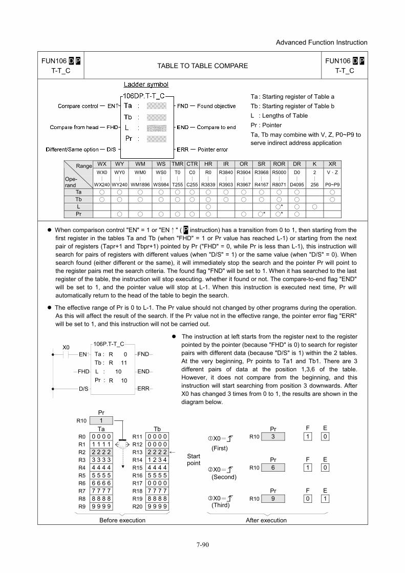
Advanced Function Instruction
7-90
FUN106 D P T-T_C
TABLE TO TABLE COMPARE FUN106 D P
T-T_C
Ta : Starting register of Table a Tb : Starting register of Table b L : Lengths of Table Pr : Pointer Ta, Tb may combine with V, Z, P0~P9 to serve indirect address application
WX WY WM WS TMR CTR HR IR OR SR ROR DR K XRRange
Ope- rand
WX0 ∣
WX240
WY0∣
WY240
WM0 ∣
WM1896
WS0 ∣
WS984
T0∣
T255
C0∣
C255
R0 ∣
R3839
R3840∣
R3903
R3904∣
R3967
R3968∣
R4167
R5000∣
R8071
D0 ∣
D4095
2 ∣
256
V、Z
P0~P9Ta ○ ○ ○ ○ ○ ○ ○ ○ ○ ○ ○ ○ ○
Tb ○ ○ ○ ○ ○ ○ ○ ○ ○ ○ ○ ○ ○
L ○ ○* ○ ○ Pr ○ ○ ○ ○ ○ ○ ○ ○* ○* ○
When comparison control "EN" = 1 or "EN↑" ( P instruction) has a transition from 0 to 1, then starting from the first register in the tables Ta and Tb (when "FHD" = 1 or Pr value has reached L-1) or starting from the next pair of registers (Tapr+1 and Tbpr+1) pointed by Pr ("FHD" = 0, while Pr is less than L-1), this instruction will search for pairs of registers with different values (when "D/S" = 1) or the same value (when "D/S" = 0). When search found (either different or the same), it will immediately stop the search and the pointer Pr will point to the register pairs met the search criteria. The found flag "FND" will be set to 1. When it has searched to the last register of the table, the instruction will stop executing. whether it found or not. The compare-to-end flag "END" will be set to 1, and the pointer value will stop at L-1. When this instruction is executed next time, Pr will automatically return to the head of the table to begin the search.
The effective range of Pr is 0 to L-1. The Pr value should not changed by other programs during the operation. As this will affect the result of the search. If the Pr value not in the effective range, the pointer error flag "ERR" will be set to 1, and this instruction will not be carried out.
X0EN Ta :
106P.T-T_C
ENDTb : R 11L :Pr :
FHD
D/S ERR
10R 10
FNDR 0
The instruction at left starts from the register next to the register pointed by the pointer (because "FHD" is 0) to search for register pairs with different data (because "D/S" is 1) within the 2 tables. At the very beginning, Pr points to Ta1 and Tb1. There are 3 different pairs of data at the position 1,3,6 of the table. However, it does not compare from the beginning, and this instruction will start searching from position 3 downwards. After X0 has changed 3 times from 0 to 1, the results are shown in the diagram below.
Pr R10 1
Ta Tb Pr F ER0 0 0 0 0 R11 0 0 0 0 R10 3 1 0 R1 1 1 1 1 R12 0 0 0 0 R2 2 2 2 2
R13 2 2 2 2 ←
R3 3 3 3 3 R14 1 2 3 4
X0= (First)
Pr F ER4 4 4 4 4 R15 4 4 4 4
Start point
R10 6 1 0 R5 5 5 5 5 R16 5 5 5 5 R6 6 6 6 6 R17 0 0 0 0 R7 7 7 7 7 R18 7 7 7 7
X0= (Second)
Pr F ER8 8 8 8 8 R19 8 8 8 8 R10 9 0 1 R9 9 9 9 9 R20 9 9 9 9
X0= (Third)
Before execution After execution
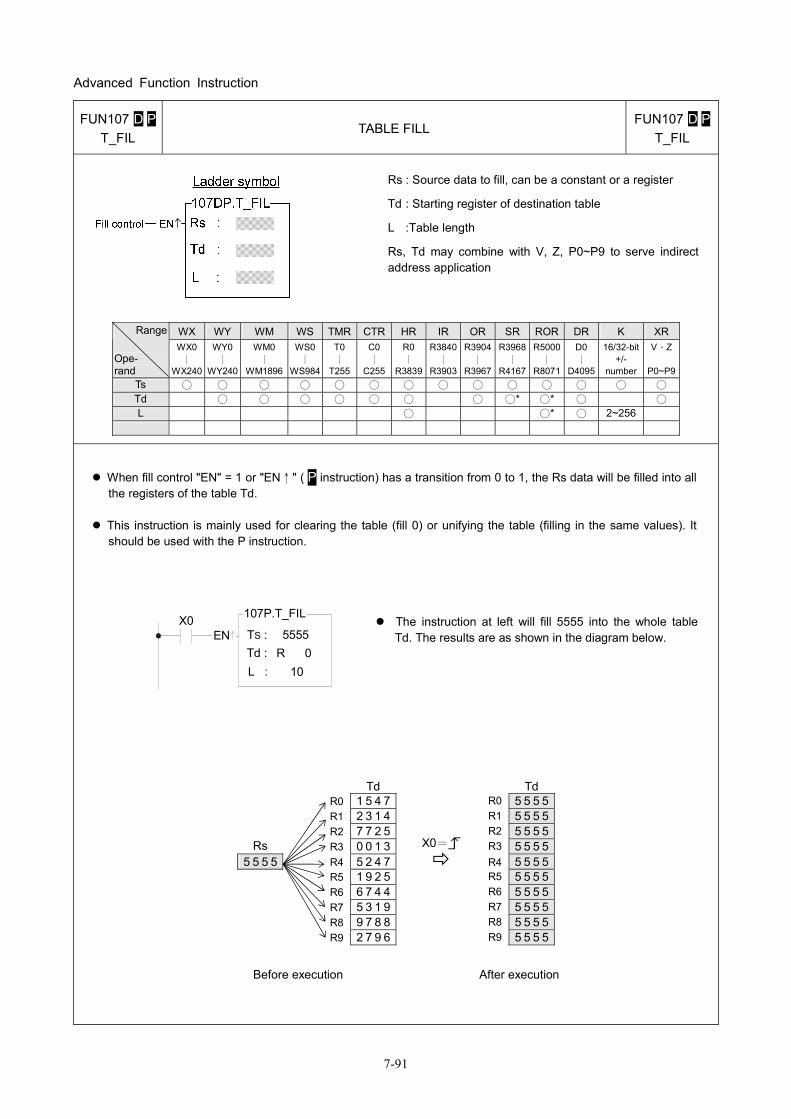
Advanced Function Instruction
7-91
FUN107 D P T_FIL
TABLE FILL FUN107 D P
T_FIL
Rs : Source data to fill, can be a constant or a register
Td : Starting register of destination table
L :Table length
Rs, Td may combine with V, Z, P0~P9 to serve indirect address application
WX WY WM WS TMR CTR HR IR OR SR ROR DR K XRRange
Ope- rand
WX0 ∣
WX240
WY0∣
WY240
WM0 ∣
WM1896
WS0 ∣
WS984
T0 ∣
T255
C0 ∣
C255
R0 ∣
R3839
R3840∣
R3903
R3904∣
R3967
R3968∣
R4167
R5000 ∣
R8071
D0 ∣
D4095
16/32-bit +/-
number
V、Z
P0~P9Ts ○ ○ ○ ○ ○ ○ ○ ○ ○ ○ ○ ○ ○ ○ Td ○ ○ ○ ○ ○ ○ ○ ○* ○* ○ ○ L ○ ○* ○ 2~256
When fill control "EN" = 1 or "EN↑" ( P instruction) has a transition from 0 to 1, the Rs data will be filled into all the registers of the table Td.
This instruction is mainly used for clearing the table (fill 0) or unifying the table (filling in the same values). It should be used with the P instruction.
X0EN TS :
Td :L :
107P.T_FIL
5555R 0
10
The instruction at left will fill 5555 into the whole table Td. The results are as shown in the diagram below.
Td Td
R0 1 5 4 7 R0 5 5 5 5 R1 2 3 1 4 R1 5 5 5 5 R2 7 7 2 5 R2 5 5 5 5
Rs R3 0 0 1 3 R3 5 5 5 55 5 5 5 R4 5 2 4 7 R4 5 5 5 5
R5 1 9 2 5 R5 5 5 5 5 R6 6 7 4 4 R6 5 5 5 5 R7 5 3 1 9
X0=
R7 5 5 5 5 R8 9 7 8 8 R8 5 5 5 5
R9 2 7 9 6 R9 5 5 5 5
Before execution After execution
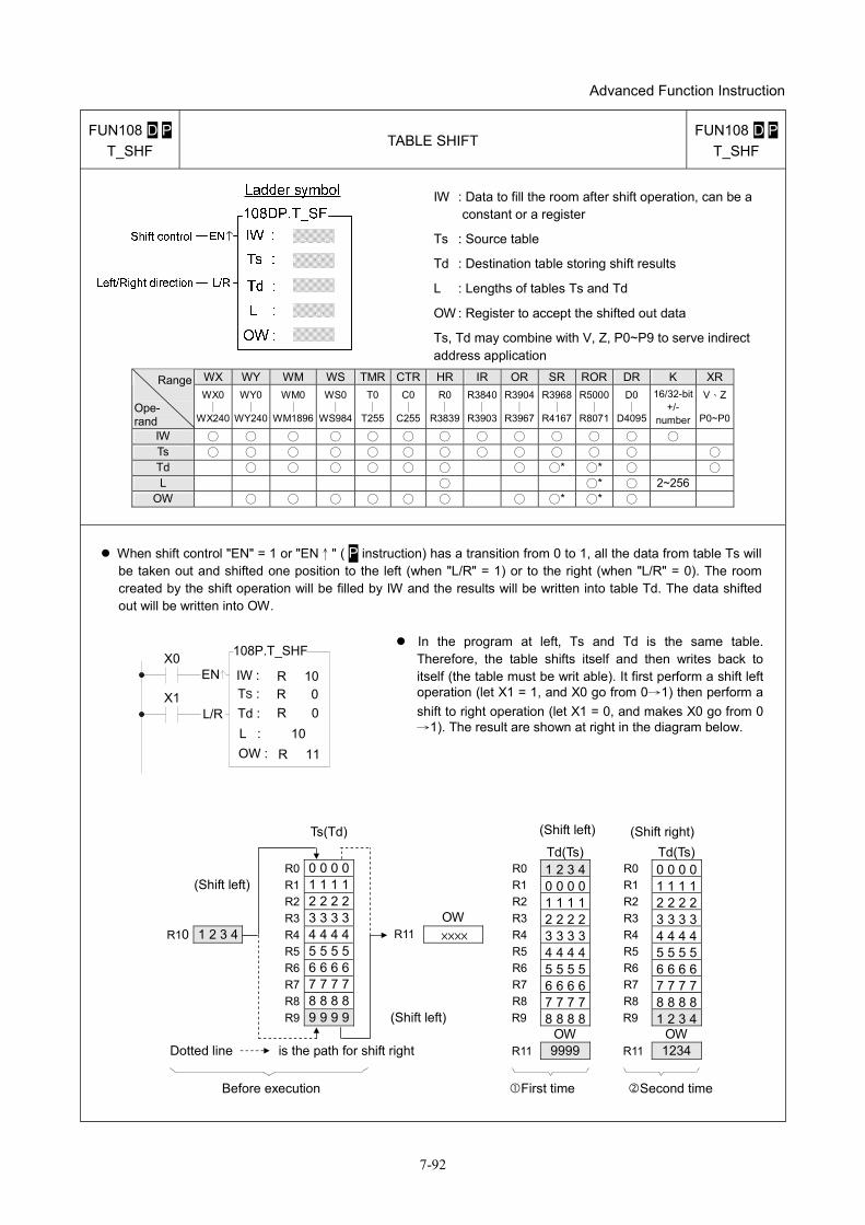
Advanced Function Instruction
7-92
FUN108 D P T_SHF
TABLE SHIFT FUN108 D P
T_SHF
IW : Data to fill the room after shift operation, can be a constant or a register
Ts : Source table
Td : Destination table storing shift results
L : Lengths of tables Ts and Td
OW : Register to accept the shifted out data
Ts, Td may combine with V, Z, P0~P9 to serve indirect address application
WX WY WM WS TMR CTR HR IR OR SR ROR DR K XRRange
Ope- rand
WX0 ∣
WX240
WY0∣
WY240
WM0 ∣
WM1896
WS0 ∣
WS984
T0 ∣
T255
C0∣
C255
R0 ∣
R3839
R3840∣
R3903
R3904∣
R3967
R3968∣
R4167
R5000∣
R8071
D0 ∣
D4095
16/32-bit +/-
number
V、Z
P0~P0
IW ○ ○ ○ ○ ○ ○ ○ ○ ○ ○ ○ ○ ○ Ts ○ ○ ○ ○ ○ ○ ○ ○ ○ ○ ○ ○ ○
Td ○ ○ ○ ○ ○ ○ ○ ○* ○* ○ ○
L ○ ○* ○ 2~256 OW ○ ○ ○ ○ ○ ○ ○ ○* ○* ○
When shift control "EN" = 1 or "EN↑" ( P instruction) has a transition from 0 to 1, all the data from table Ts will be taken out and shifted one position to the left (when "L/R" = 1) or to the right (when "L/R" = 0). The room created by the shift operation will be filled by IW and the results will be written into table Td. The data shifted out will be written into OW.
X0EN
TS :Td :
R 11L :OW :
L/R10
R 10R 0
IW :
R 0X1
108P.T_SHF
In the program at left, Ts and Td is the same table. Therefore, the table shifts itself and then writes back to itself (the table must be writ able). It first perform a shift left operation (let X1 = 1, and X0 go from 0→1) then perform a shift to right operation (let X1 = 0, and makes X0 go from 0→1). The result are shown at right in the diagram below.
Ts(Td) (Shift left) (Shift right) Td(Ts) Td(Ts) R0 0 0 0 0 R0 1 2 3 4 R0 0 0 0 0 (Shift left) R1 1 1 1 1 R1 0 0 0 0 R1 1 1 1 1 R2 2 2 2 2 R2 1 1 1 1 R2 2 2 2 2 R3 3 3 3 3 OW R3 2 2 2 2 R3 3 3 3 3
R10 1 2 3 4 R4 4 4 4 4 R11 ×××× R4 3 3 3 3 R4 4 4 4 4 R5 5 5 5 5 R5 4 4 4 4 R5 5 5 5 5 R6 6 6 6 6 R6 5 5 5 5 R6 6 6 6 6 R7 7 7 7 7 R7 6 6 6 6 R7 7 7 7 7 R8 8 8 8 8 R8 7 7 7 7 R8 8 8 8 8 R9 9 9 9 9 (Shift left) R9 8 8 8 8 R9 1 2 3 4 OW OW
Dotted line is the path for shift right R11 9999 R11 1234
Before execution First time Second time
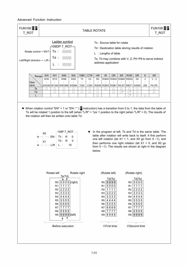
Advanced Function Instruction
7-93
FUN109 D P T_ROT
TABLE ROTATE FUN109 D P
T_ROT
Ts :ENRotate control
Ladder symbol 109DP.T_ROT
Td :
L :L/RLeft/Right direction
Ts : Source table for rotate
Td : Destination table storing results of rotation
L : Lengths of table
Ts, Td may combine with V, Z, P0~P9 to serve indirect address application
WX WY WM WS TMR CTR HR IR OR SR ROR DR K XR Range
Ope- rand
WX0 ∣
WX240
WY0∣
WY240
WM0 ∣
WM1896
WS0 ∣
WS984
T0 ∣
T255
C0 ∣
C255
R0 ∣
R3839
R3840∣
R3903
R3904∣
R3967
R3968∣
R4167
R5000∣
R8071
D0 ∣
D4095
2 ∣
256
V、Z P0~P9
Ts ○ ○ ○ ○ ○ ○ ○ ○ ○ ○ ○ ○ ○ Td ○ ○ ○ ○ ○ ○ ○ ○* ○* ○ ○ L ○ ○* ○ ○
When rotation control "EN" = 1 or "EN↑" ( P instruction) has a transition from 0 to 1, the data from the table of Ts will be rotated 1 position to the left (when "L/R" = 1)or 1 position to the right (when "L/R" = 0). The results of the rotation will then be written onto table Td.
X0EN TS :
Td :L :L/R
X1
109P.T_ROT
10
R 0R 0
In the program at left, Ts and Td is the same table. The table after rotation will write back to itself. It first perform one left rotation (let X1 = 1, and X0 go from 0→1), and then performs one right rotation (let X1 = 0, and X0 go from 0→1). The results are shown at right in the diagram below.
Rotate left Rotate right (Rotate left) (Rotate right) Ts(Td)
Td(Ts) Td(Ts) R0 0 0 0 0 (right) R0 9 9 9 9 R0 0 0 0 0 R1 1 1 1 1 R1 0 0 0 0 R1 1 1 1 1 R2 2 2 2 2 R2 1 1 1 1 R2 2 2 2 2 R3 3 3 3 3 R3 2 2 2 2 R3 3 3 3 3
R4 4 4 4 4 R4 3 3 3 3 R4 4 4 4 4 R5 5 5 5 5 R5 4 4 4 4 R5 5 5 5 5
R6 6 6 6 6 R6 5 5 5 5 R6 6 6 6 6 R7 7 7 7 7 R7 6 6 6 6 R7 7 7 7 7 R8 8 8 8 8 R8 7 7 7 7 R8 8 8 8 8 R9 9 9 9 9 (left) R9 8 8 8 8 R9 9 9 9 9
Before execution First time Second time
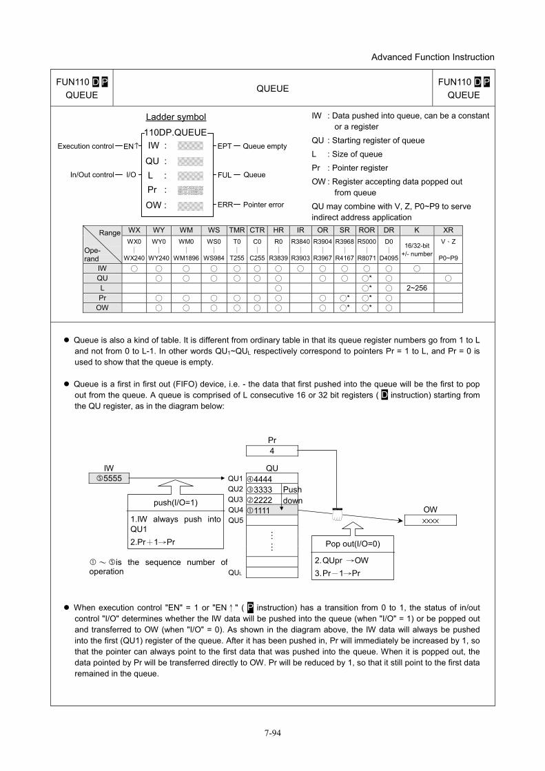
Advanced Function Instruction
7-94
FUN110 D P QUEUE
QUEUE FUN110 D P
QUEUE
IW :ENExecution control
Ladder symbol
110DP.QUEUE
QU :
EPT Queue empty
FUL QueueIn/Out control I/O L :Pr :
ERR Pointer errorOW :
IW : Data pushed into queue, can be a constant or a register
QU : Starting register of queue
L : Size of queue
Pr : Pointer register
OW : Register accepting data popped out from queue
QU may combine with V, Z, P0~P9 to serve indirect address application
WX WY WM WS TMR CTR HR IR OR SR ROR DR K XR Range
Ope- rand
WX0 ∣
WX240
WY0∣
WY240
WM0 ∣
WM1896
WS0 ∣
WS984
T0∣
T255
C0∣
C255
R0∣
R3839
R3840∣
R3903
R3904∣
R3967
R3968∣
R4167
R5000∣
R8071
D0 ∣
D4095
16/32-bit +/- number
V、Z
P0~P9IW ○ ○ ○ ○ ○ ○ ○ ○ ○ ○ ○ ○ ○ QU ○ ○ ○ ○ ○ ○ ○ ○ ○* ○ ○ L ○ ○* ○ 2~256 Pr ○ ○ ○ ○ ○ ○ ○ ○* ○* ○
OW ○ ○ ○ ○ ○ ○ ○ ○* ○* ○
Queue is also a kind of table. It is different from ordinary table in that its queue register numbers go from 1 to L and not from 0 to L-1. In other words QU1~QUL respectively correspond to pointers Pr = 1 to L, and Pr = 0 is used to show that the queue is empty.
Queue is a first in first out (FIFO) device, i.e. - the data that first pushed into the queue will be the first to pop out from the queue. A queue is comprised of L consecutive 16 or 32 bit registers ( D instruction) starting from the QU register, as in the diagram below:
Pr 4
IW QU 5555 QU1 4444
QU2 3333 QU3 2222 QU4 1111 OW
QU5 ××××
~ is the sequence number of
operation QUL
When execution control "EN" = 1 or "EN↑" ( P instruction) has a transition from 0 to 1, the status of in/out control "I/O" determines whether the IW data will be pushed into the queue (when "I/O" = 1) or be popped out and transferred to OW (when "I/O" = 0). As shown in the diagram above, the IW data will always be pushed into the first (QU1) register of the queue. After it has been pushed in, Pr will immediately be increased by 1, so that the pointer can always point to the first data that was pushed into the queue. When it is popped out, the data pointed by Pr will be transferred directly to OW. Pr will be reduced by 1, so that it still point to the first data remained in the queue.
push(I/O=1) 1.IW always push into QU1 2.Pr+1→Pr
Push down
Pop out(I/O=0) 2. QUpr →OW 3. Pr-1→Pr
… …
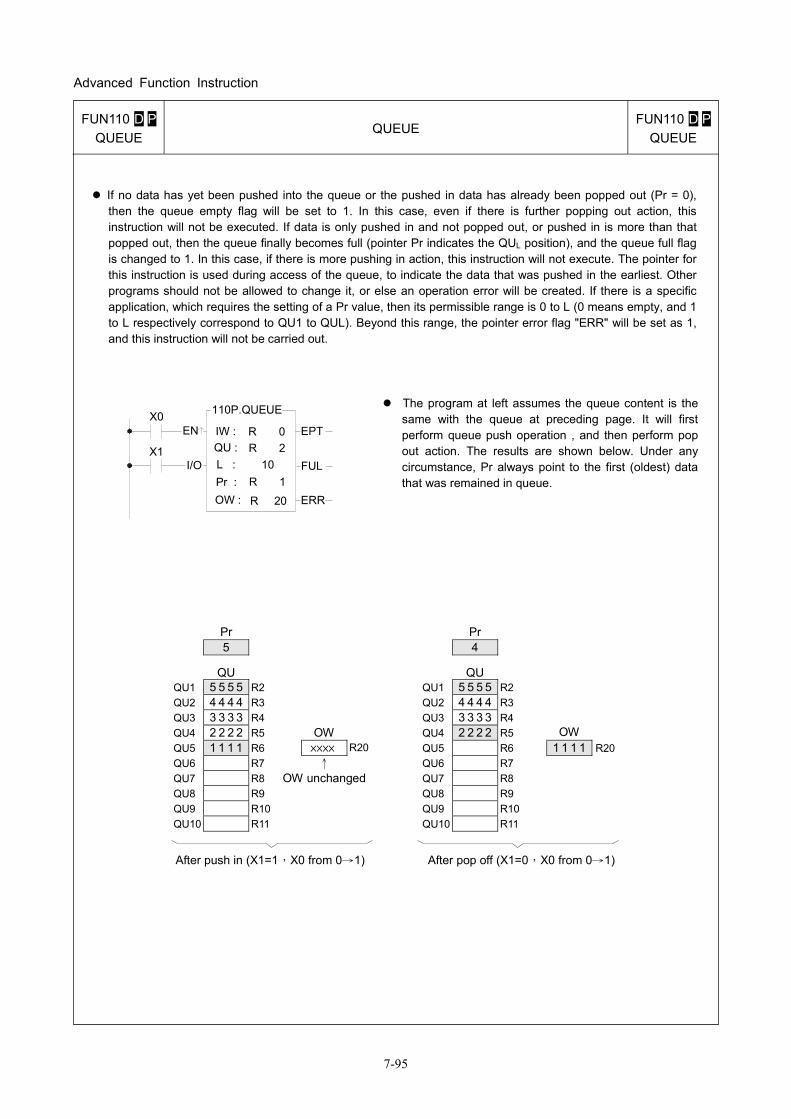
Advanced Function Instruction
7-95
FUN110 D P QUEUE
QUEUE FUN110 D P
QUEUE
If no data has yet been pushed into the queue or the pushed in data has already been popped out (Pr = 0), then the queue empty flag will be set to 1. In this case, even if there is further popping out action, this instruction will not be executed. If data is only pushed in and not popped out, or pushed in is more than that popped out, then the queue finally becomes full (pointer Pr indicates the QUL position), and the queue full flag is changed to 1. In this case, if there is more pushing in action, this instruction will not execute. The pointer for this instruction is used during access of the queue, to indicate the data that was pushed in the earliest. Other programs should not be allowed to change it, or else an operation error will be created. If there is a specific application, which requires the setting of a Pr value, then its permissible range is 0 to L (0 means empty, and 1 to L respectively correspond to QU1 to QUL). Beyond this range, the pointer error flag "ERR" will be set as 1, and this instruction will not be carried out.
X0EN
QU :
110P.QUEUE
Pr :R 20
L :
OW :
I/O 10R 2
IW :
R 1
X1
R 0
FUL
ERR
EPT
The program at left assumes the queue content is the same with the queue at preceding page. It will first perform queue push operation , and then perform pop out action. The results are shown below. Under any circumstance, Pr always point to the first (oldest) data that was remained in queue.
Pr Pr 5 4
QU QU QU1 5 5 5 5 R2 QU1 5 5 5 5 R2QU2 4 4 4 4 R3 QU2 4 4 4 4 R3QU3 3 3 3 3 R4 QU3 3 3 3 3 R4QU4 2 2 2 2 R5 OW QU4 2 2 2 2 R5 OW QU5 1 1 1 1 R6 ×××× R20 QU5 R6 1 1 1 1 R20 QU6 R7 ↑ QU6 R7QU7 R8 OW unchanged QU7 R8QU8 R9 QU8 R9QU9 R10 QU9 R10QU10 R11 QU10 R11
After push in (X1=1,X0 from 0→1) After pop off (X1=0,X0 from 0→1)
Advanced Function Instruction
7-96
FUN111 D P STACK
STACK FUN111 D P
STACK
IW :ENExecution control
Ladder symbol
111DP.STACK
ST :
EPT Stack empty
FUL Stack fullIn/Out control I/O L :Pr :
ERR Pointer errorOW :
IW : Data pushed into stack, can be a constant or a register
ST : Starting register of stack L : Size of stack Pr : Pointer register OW : Register accepting data popped out from
stack ST may combine with V, Z, P0~P9 to serve indirect address application
WX WY WM WS TMR CTR HR IR OR SR ROR DR K XR Range
Ope- rand
WX0 ∣
WX240
WY0 ∣
WY240
WM0 ∣
WM1896
WS0 ∣
WS984
T0 ∣
T255
C0 ∣
C255
R0 ∣
R3839
R3840∣
R3903
R3904∣
R3967
R3968∣
R4167
R5000 ∣
R8071
D0 ∣
D4095
16/32-bit +/-
number
V、Z
P0~P9IW ○ ○ ○ ○ ○ ○ ○ ○ ○ ○ ○ ○ ○ ST ○ ○ ○ ○ ○ ○ ○ ○* ○* ○ ○ L ○ ○* ○ 2~256 Pr ○ ○ ○ ○ ○ ○ ○ ○* ○* ○
OW ○ ○ ○ ○ ○ ○ ○ ○* ○* ○
Like queue, stack is also a kind of table. The nature of its pointer is exactly the same as with queue, i.e. Pr = 1 to L, which corresponds to ST1 to STL, and when Pr = 0 the stack is empty.
Stack is the opposite of queue, being a last in first out (LIFO) device. This means that the data that was most recently pushed into the stack will be the first to be popped out of the stack. The stack is comprised of L consecutive 16 or 32-bit ( D instruction) registers starting from ST, as shown in the following diagram:
Pr 4
~ is the sequence number of operation ST
ST1 1111 ← Bottom of stack ST2 2222 ST3 3333
IW ST4 4444 OW 5555 ST5 ××××
push
STL
When execution control "EN" = 1 or "EN↑" ( P instruction) has a transition from 0 to 1, the status of in/out control "I/O" determines whether the IW data will be pushed into the stack (when "I/O" = 1), or the data pointed by Pr within the stack (the data most recently pushed into the stack) will be moved out and transferred to OW (when "I/O" = 0). Note that the data pushed in is stacking, so before pushed in, Pr will increased by 1 to point to the top of the stack then the data will be pushed in. When it is popped out, the data pointed by pointer Pr (the most recently pushed in data) will be transferred to OW. After then Pr will decreased by 1. Under any circumstances, the pointer Pr will always point to the data that was pushed into the stack most recently.
push(I/O=1) 1.Pr+1→Pr 2.IW→STpr
pop(I/O=0) 1.STpr→OW 2.Pr-1→Pr
Advanced Function Instruction
7-97
FUN111 D P STACK
STACK FUN111 D P
STACK
When no data has yet been pushed into the stack or the pushed in data has already been popped out (Pr = 0), the stack empty flag "EPT" will set to 1. In this case any further pop up actions, will be ignored. If more data is pushed than popped out, sooner or latter the stack will be full (pointer Pr points to STL position), and the stack full flag "FUL" will set to 1. In this case any further push actions, will be ignored. As with queue, the stack pointer in normal case should not be changed by other instructions. If there is a special application which requires to set the Pr value, then its effective range is 0 to L (0 means empty, 1 to L respectively correspond to ST1 to STL). Beyond this range, the pointer error flag "ERR" will set to 1, and the instruction will not be carried out.
X0EN
ST :
111P.STACK
Pr :R 20
L :
OW :
I/O 10R 2
IW :
R 1
X1
R 0
FUL
ERR
EPT
The program at left assumes that the initial content of the stack is just as in the diagram of a stack on the preceding page. The operation illustrated in this example is to push a data and than pop it from stack. The results are shown below. Under any circumstances, Pr always point to the data that was most recently pushed into the stack.
Pr Pr 5 R1 4
ST QU ST1 1 1 1 1 R2 ST1 1 1 1 1 R2ST2 2 2 2 2 R3 ST2 2 2 2 2 R3ST3 3 3 3 3 R4 ST3 3 3 3 3 R4ST4 4 4 4 4 R5 OW ST4 4 4 4 4 R5 OW ST5 5 5 5 5 R6 ×××× R20 ST5 R6 5 5 5 5 R20 ST6 R7 ↑ ST6 R7ST7 R8 OW unchanged ST7 R8ST8 R9 ST8 R9ST9 R10 ST9 R10ST10 R11 ST10 R11
After push(X1=1,X0 from 0→1) After pop up(X1=0,X0 from 0→1)
Advanced Function Instruction
7-98
FUN112 D P BKCMP
BLOCK COMPARE(DRUM) FUN112 D P
BKCMP
Rs : Data for compare, can be a constant or a register
Ts : Starting register block storing upper and lower limit
L : Number of pairs of upper and lower limits
D : Starting relay storing results of comparison
Y M S WX WY WM WS TMR CTR HR IR OR SR ROR DR K Range
Ope- rand
Y0 ∣
Y255
M0 ∣
M999
S0 ∣
S999
WX0 ∣
WX240
WY0 ∣
WY240
WM0 ∣
WM1896
WS0∣
WS984
T0∣
T255
C0∣
C255
R0 ∣
R3839
R3840∣
R3903
R3904∣
R3967
R3968 ∣
R4167
R5000 ∣
R8071
D0 ∣
D4095
16/32-bit+/-
numberRs ○ ○ ○ ○ ○ ○ ○ ○ ○ ○ ○ ○ ○ Ts ○ ○ ○ ○ ○ ○ ○ ○ ○ ○ ○ ○ L ○ ○* ○ 1~256D ○ ○ ○
When comparison control "EN" = 1 or "EN↑" ( P instruction) has a transition from 0 to 1, comparisons will be perform one by one between the contents of Rs and the upper and lower limits form by L pairs of 16 or 32-bit ( D modifier) registers starting from the Ts register (starting from T0 each adjoining 2 register units form a pair of upper and lower limits). If the value of Rs falls within the range of the pair, then the bit within the comparison results relay D which corresponds to that pair will be set to 1. Otherwise it will be set as 0 until comparison of all the L pairs of upper and lower limits is completed.
When M1975=0, if there is any pair where the upper limit value is less than the lower limit value, then the limit error flag "ERR" will be set to 1, and the comparison output for that pair will be 0.
When M1975=1, there is no restriction on the relation of upper limit and lower limit, this can apply for 360°rotary electronic drum switch application.
Upper limit Lower limit Result Compare
Compared value
0 TS1 TS0 D0
1 TS3 TS2 D1
L−1 TS2L−1 TS2L−2
Rs
DL−1
Actually this instruction is a drum switch, which can be used in interrupt program and when incorporate with immediate I/O instruction (IMDIO) can achieve an accurate electronic drum.
X0EN RS :
Ts :
Y 5
112.BKCMP
D :
C 0
L : 4
ERR
R 10
CLRC0
CKX1
C 0PV : 360
In this program, C0 represents the rotation angle (Rs) of a drum shaft. The block compare instruction performs a comparison between Rs and the 4 pairs (L = 4) of upper and lower limits, R10,R11, R12,R13, R14,R15 and R16,R17. The comparison results can be obtained from the four drum output points Y5 to Y8.
The input point X1 is a rotation angle detector mounted on the drum shaft. With each one degree rotation of the drum shaft angle, X1 produces a pulse. When the drum shaft rotates a full cycle, X1 produces 360 pulses.
Advanced Function Instruction
7-99
FUN112 D P BKCMP
BLOCK COMPARE(DRUM) FUN112 D P
BKCMP
The program in the diagram above coordinates a rotary encoder or other rotating angle detection device (directly connect to a rotating mechanism), which can form a mechanical device equivalent to the mechanical structure of an actual drum (see mechanism shown within dotted line in diagram below). While the upper and lower limits are being adjusted, you can change at will the range of the activated angle of the drum. This cannot be done with the traditional drum mechanism.
Equivalent mechanical drum emulated by above program
X1
8090
40
Limit sw
320
0
Y5
140
180
220
180
Y6
60
Y7
200
80
Y8
Rotary encoder
Rotating . mechanism
Y5
Y6
Y7
Y8
C0
40 140
80 180
60
80 200
0° 40° 80° 120° 160° 200° 240° 280° 320° 360°
X1 Y5 Y6 Y7 Y8
Rotary encoder
Rotating mechanism
Limit sw
320
220
40
180 140
180
8090
0
60
80
200
0
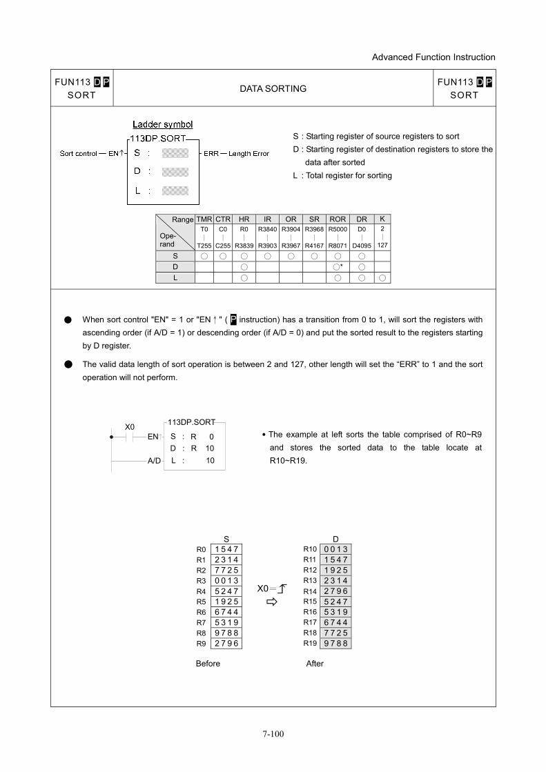
Advanced Function Instruction
7-100
FUN113 D P SORT
DATA SORTING FUN113 D P
SORT
S : Starting register of source registers to sort D : Starting register of destination registers to store the
data after sorted L : Total register for sorting
TMR CTR HR IR OR SR ROR DR KRange
Ope- rand
T0 ∣
T255
C0∣
C255
R0 ∣
R3839
R3840∣
R3903
R3904∣
R3967
R3968∣
R4167
R5000∣
R8071
D0 ∣
D4095
2∣
127
S ○ ○ ○ ○ ○ ○ ○ ○ D ○ ○* ○ L ○ ○ ○ ○
● When sort control "EN" = 1 or "EN↑" ( P instruction) has a transition from 0 to 1, will sort the registers with ascending order (if A/D = 1) or descending order (if A/D = 0) and put the sorted result to the registers starting by D register.
● The valid data length of sort operation is between 2 and 127, other length will set the “ERR” to 1 and the sort operation will not perform.
X0EN R 0
A/D
113DP.SORT
D :S :
L :R 10
10
˙The example at left sorts the table comprised of R0~R9 and stores the sorted data to the table locate at R10~R19.
S D R0 1 5 4 7 R10 0 0 1 3R1 2 3 1 4 R11 1 5 4 7R2 7 7 2 5 R12 1 9 2 5R3 0 0 1 3 R13 2 3 1 4R4 5 2 4 7 R14 2 7 9 6R5 1 9 2 5 R15 5 2 4 7R6 6 7 4 4 R16 5 3 1 9R7 5 3 1 9 R17 6 7 4 4R8 9 7 8 8 R18 7 7 2 5R9 2 7 9 6
X0=
R19 9 7 8 8
Before After
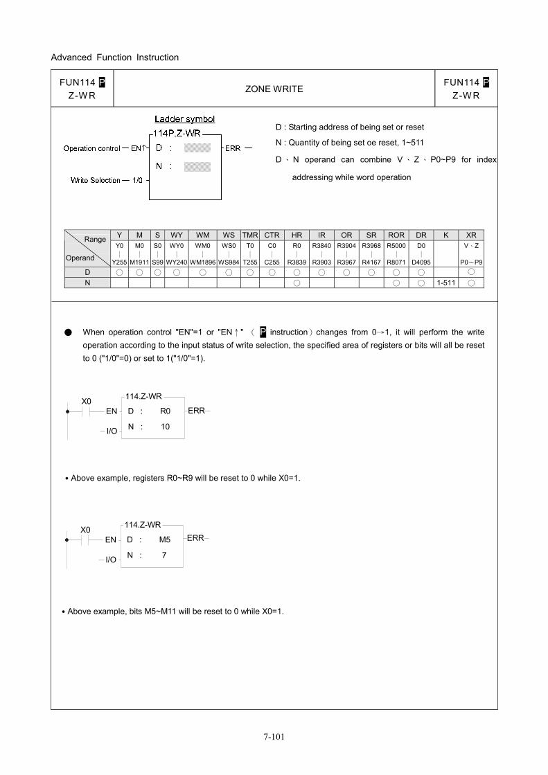
Advanced Function Instruction
7-101
FUN114 P Z-W R
ZONE WRITE FUN114 P
Z-W R
D : Starting address of being set or reset
N : Quantity of being set oe reset, 1~511
D 、 N operand can combine V 、 Z 、 P0~P9 for index
addressing while word operation
Y M S WY WM WS TMR CTR HR IR OR SR ROR DR K XR Range
Operand
Y0 ∣
Y255
M0 ∣
M1911
S0∣
S99
WY0 ∣
WY240
WM0 ∣
WM1896
WS0∣
WS984
T0∣
T255
C0 ∣
C255
R0 ∣
R3839
R3840∣
R3903
R3904∣
R3967
R3968∣
R4167
R5000 ∣
R8071
D0 ∣
D4095
V、Z
P0~P9D ○ ○ ○ ○ ○ ○ ○ ○ ○ ○ ○ ○ ○ ○ ○ N ○ ○ ○ 1-511 ○
● When operation control "EN"=1 or "EN↑" ( P instruction)changes from 0→1, it will perform the write operation according to the input status of write selection, the specified area of registers or bits will all be reset to 0 ("1/0"=0) or set to 1("1/0"=1).
X0EN
114.Z-WR
R0
N : 10I/O
D : ERR
˙Above example, registers R0~R9 will be reset to 0 while X0=1.
X0EN
114.Z-WR
M5
N : 7I/O
D : ERR
˙Above example, bits M5~M11 will be reset to 0 while X0=1.
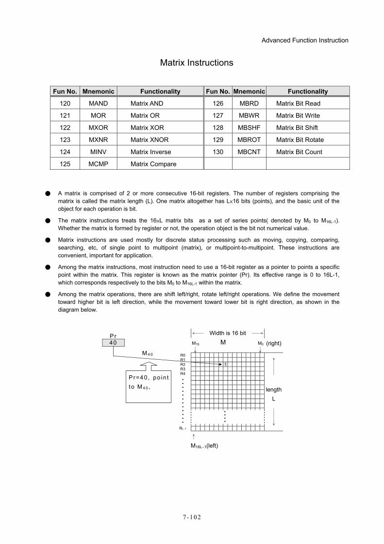
Advanced Function Instruction
7-102
Matrix Instructions
Fun No. Mnemonic Functionality Fun No. Mnemonic Functionality
120 MAND Matrix AND 126 MBRD Matrix Bit Read
121 MOR Matrix OR 127 MBWR Matrix Bit Write
122 MXOR Matrix XOR 128 MBSHF Matrix Bit Shift
123 MXNR Matrix XNOR 129 MBROT Matrix Bit Rotate
124 MINV Matrix Inverse 130 MBCNT Matrix Bit Count
125 MCMP Matrix Compare
● A matrix is comprised of 2 or more consecutive 16-bit registers. The number of registers comprising the matrix is called the matrix length (L). One matrix altogether has L×16 bits (points), and the basic unit of the object for each operation is bit.
● The matrix instructions treats the 16×L matrix bits as a set of series points( denoted by M0 to M16L-1). Whether the matrix is formed by register or not, the operation object is the bit not numerical value.
● Matrix instructions are used mostly for discrete status processing such as moving, copying, comparing, searching, etc, of single point to multipoint (matrix), or multipoint-to-multipoint. These instructions are convenient, important for application.
● Among the matrix instructions, most instruction need to use a 16-bit register as a pointer to points a specific point within the matrix. This register is known as the matrix pointer (Pr). Its effective range is 0 to 16L-1, which corresponds respectively to the bits M0 to M16L-1 within the matrix.
● Among the matrix operations, there are shift left/right, rotate left/right operations. We define the movement toward higher bit is left direction, while the movement toward lower bit is right direction, as shown in the diagram below.
←─ Width is 16 bit ─→
M15
↓M M0
↓(right)
R0R1R2 1R3R4
RL−1
↑ │ │
length L
│ │ ↓
↑ M16L−1(left)
Pr=40, po in t to M 4 0 ,
Pr40
M 4 0
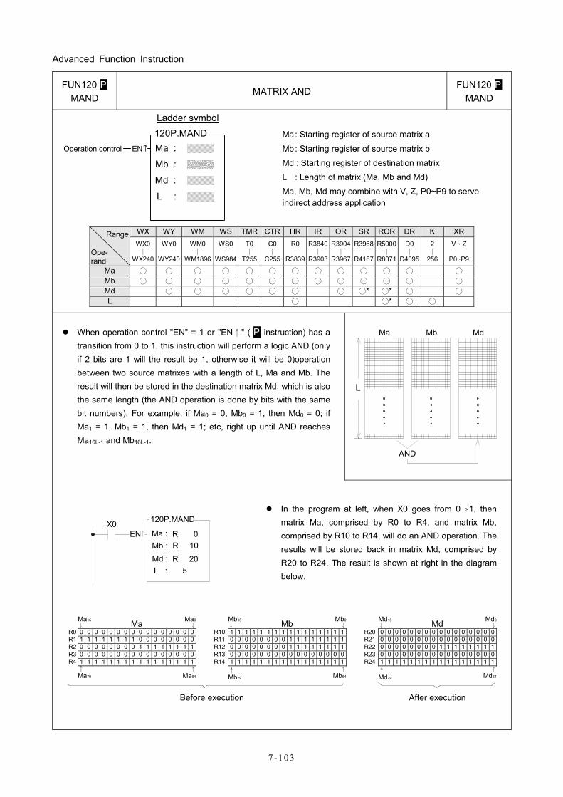
Advanced Function Instruction
7 -103
FUN120 P MAND
MATRIX AND FUN120 P
MAND
Ma :EN Operation control
Ladder symbol 120P.MAND
Mb :
L :
Md :
Ma : Starting register of source matrix a
Mb : Starting register of source matrix b
Md : Starting register of destination matrix
L : Length of matrix (Ma, Mb and Md)
Ma, Mb, Md may combine with V, Z, P0~P9 to serve indirect address application
WX WY WM WS TMR CTR HR IR OR SR ROR DR K XR Range
Ope- rand
WX0 ∣
WX240
WY0 ∣
WY240
WM0 ∣
WM1896
WS0∣
WS984
T0 ∣
T255
C0∣
C255
R0∣
R3839
R3840∣
R3903
R3904∣
R3967
R3968∣
R4167
R5000∣
R8071
D0 ∣
D4095
2 ∣
256
V、Z
P0~P9
Ma ○ ○ ○ ○ ○ ○ ○ ○ ○ ○ ○ ○ ○ Mb ○ ○ ○ ○ ○ ○ ○ ○ ○ ○ ○ ○ ○ Md ○ ○ ○ ○ ○ ○ ○ ○* ○* ○ ○ L ○ ○* ○ ○
When operation control "EN" = 1 or "EN↑" ( P instruction) has a transition from 0 to 1, this instruction will perform a logic AND (only if 2 bits are 1 will the result be 1, otherwise it will be 0)operation between two source matrixes with a length of L, Ma and Mb. The result will then be stored in the destination matrix Md, which is also the same length (the AND operation is done by bits with the same bit numbers). For example, if Ma0 = 0, Mb0 = 1, then Md0 = 0; if Ma1 = 1, Mb1 = 1, then Md1 = 1; etc, right up until AND reaches Ma16L-1 and Mb16L-1.
Ma Mb
AND
Md
L
X0EN R 0
120P.MAND
L :
Ma :Mb :Md :
R 10R 20
5
In the program at left, when X0 goes from 0→1, then matrix Ma, comprised by R0 to R4, and matrix Mb, comprised by R10 to R14, will do an AND operation. The results will be stored back in matrix Md, comprised by R20 to R24. The result is shown at right in the diagram below.
Ma15 ↓ Ma Ma0
↓Mb15 ↓ Mb Mb0
↓Md15 ↓ Md Md0
↓R0 0 0 0 0 0 0 0 0 0 0 0 0 0 0 0 0 R10 1 1 1 1 1 1 1 1 1 1 1 1 1 1 1 1 R20 0 0 0 0 0 0 0 0 0 0 0 0 0 0 0 0R1 1 1 1 1 1 1 1 1 0 0 0 0 0 0 0 0 R11 0 0 0 0 0 0 0 0 1 1 1 1 1 1 1 1 R21 0 0 0 0 0 0 0 0 0 0 0 0 0 0 0 0R2 0 0 0 0 0 0 0 0 1 1 1 1 1 1 1 1 R12 0 0 0 0 0 0 0 0 1 1 1 1 1 1 1 1 R22 0 0 0 0 0 0 0 0 1 1 1 1 1 1 1 1R3 0 0 0 0 0 0 0 0 0 0 0 0 0 0 0 0 R13 0 0 0 0 0 0 0 0 0 0 0 0 0 0 0 0 R23 0 0 0 0 0 0 0 0 0 0 0 0 0 0 0 0R4 1 1 1 1 1 1 1 1 1 1 1 1 1 1 1 1 R14 1 1 1 1 1 1 1 1 1 1 1 1 1 1 1 1 R24 1 1 1 1 1 1 1 1 1 1 1 1 1 1 1 1
↑ Ma79
↑
Ma64↑ Mb79
↑
Mb64↑ Md79
↑
Md64
Before execution After execution
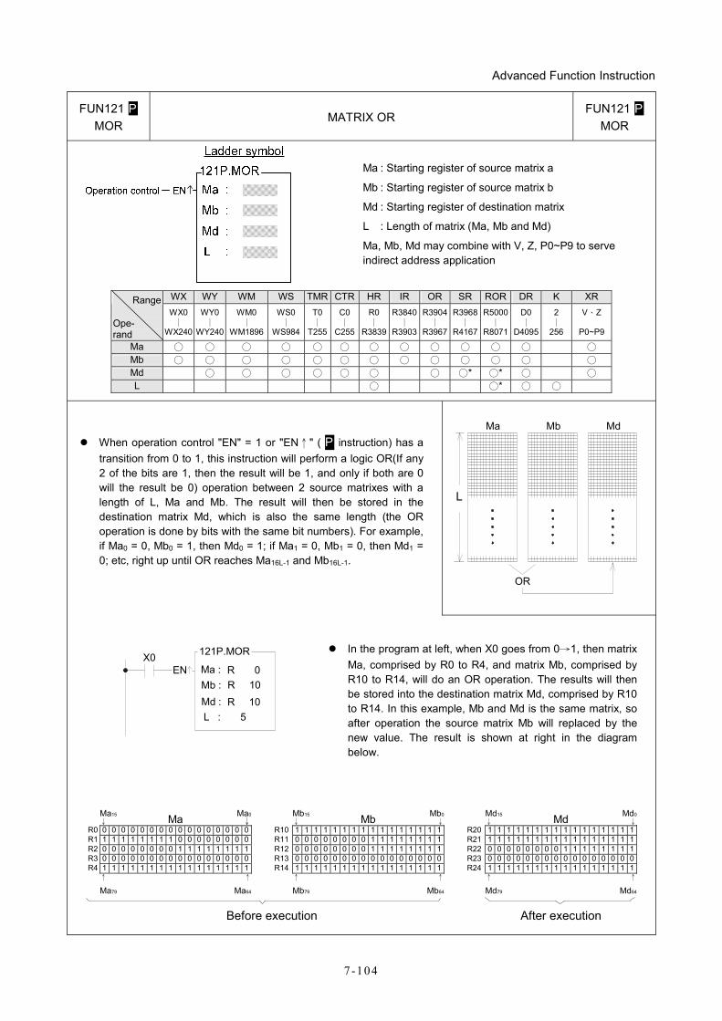
Advanced Function Instruction
7 -104
FUN121 P MOR
MATRIX OR FUN121 P
MOR
Ma : Starting register of source matrix a
Mb : Starting register of source matrix b
Md : Starting register of destination matrix
L : Length of matrix (Ma, Mb and Md)
Ma, Mb, Md may combine with V, Z, P0~P9 to serve indirect address application
WX WY WM WS TMR CTR HR IR OR SR ROR DR K XR Range
Ope- rand
WX0 ∣
WX240
WY0∣
WY240
WM0 ∣
WM1896
WS0 ∣
WS984
T0∣
T255
C0∣
C255
R0 ∣
R3839
R3840∣
R3903
R3904∣
R3967
R3968∣
R4167
R5000∣
R8071
D0 ∣
D4095
2 ∣
256
V、Z
P0~P9
Ma ○ ○ ○ ○ ○ ○ ○ ○ ○ ○ ○ ○ ○ Mb ○ ○ ○ ○ ○ ○ ○ ○ ○ ○ ○ ○ ○ Md ○ ○ ○ ○ ○ ○ ○ ○* ○* ○ ○ L ○ ○* ○ ○
When operation control "EN" = 1 or "EN↑" ( P instruction) has a transition from 0 to 1, this instruction will perform a logic OR(If any 2 of the bits are 1, then the result will be 1, and only if both are 0 will the result be 0) operation between 2 source matrixes with a length of L, Ma and Mb. The result will then be stored in the destination matrix Md, which is also the same length (the OR operation is done by bits with the same bit numbers). For example, if Ma0 = 0, Mb0 = 1, then Md0 = 1; if Ma1 = 0, Mb1 = 0, then Md1 = 0; etc, right up until OR reaches Ma16L-1 and Mb16L-1.
L
Ma Mb Md
OR
X0EN Ma :
Mb :
L : 5
R 10R 0
Md :
121P.MOR
R 10
In the program at left, when X0 goes from 0→1, then matrix Ma, comprised by R0 to R4, and matrix Mb, comprised by R10 to R14, will do an OR operation. The results will then be stored into the destination matrix Md, comprised by R10 to R14. In this example, Mb and Md is the same matrix, so after operation the source matrix Mb will replaced by the new value. The result is shown at right in the diagram below.
Ma15 ↓ Ma Ma0
↓Mb15 ↓ Mb Mb0
↓Md15 ↓ Md Md0
↓R0 0 0 0 0 0 0 0 0 0 0 0 0 0 0 0 0 R10 1 1 1 1 1 1 1 1 1 1 1 1 1 1 1 1 R20 1 1 1 1 1 1 1 1 1 1 1 1 1 1 1 1R1 1 1 1 1 1 1 1 1 0 0 0 0 0 0 0 0 R11 0 0 0 0 0 0 0 0 1 1 1 1 1 1 1 1 R21 1 1 1 1 1 1 1 1 1 1 1 1 1 1 1 1R2 0 0 0 0 0 0 0 0 1 1 1 1 1 1 1 1 R12 0 0 0 0 0 0 0 0 1 1 1 1 1 1 1 1 R22 0 0 0 0 0 0 0 0 1 1 1 1 1 1 1 1R3 0 0 0 0 0 0 0 0 0 0 0 0 0 0 0 0 R13 0 0 0 0 0 0 0 0 0 0 0 0 0 0 0 0 R23 0 0 0 0 0 0 0 0 0 0 0 0 0 0 0 0R4 1 1 1 1 1 1 1 1 1 1 1 1 1 1 1 1 R14 1 1 1 1 1 1 1 1 1 1 1 1 1 1 1 1 R24 1 1 1 1 1 1 1 1 1 1 1 1 1 1 1 1
↑
Ma79
↑
Ma64
↑
Mb79
↑
Mb64
↑
Md79
↑
Md64
Before execution After execution
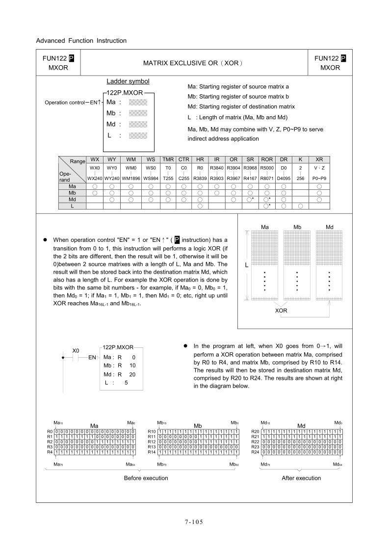
Advanced Function Instruction
7 -105
FUN122 P MXOR
MATRIX EXCLUSIVE OR(XOR) FUN122 P
MXOR
Ma :EN Operation control
Ladder symbol
122P.MXOR
Mb :
L :
Md :
Ma : Starting register of source matrix a
Mb : Starting register of source matrix b
Md : Starting register of destination matrix
L : Length of matrix (Ma, Mb and Md)
Ma, Mb, Md may combine with V, Z, P0~P9 to serve indirect address application
WX WY WM WS TMR CTR HR IR OR SR ROR DR K XR Range
Ope- rand
WX0 ∣
WX240
WY0∣
WY240
WM0 ∣
WM1896
WS0 ∣
WS984
T0 ∣
T255
C0∣
C255
R0 ∣
R3839
R3840∣
R3903
R3904∣
R3967
R3968∣
R4167
R5000∣
R8071
D0 ∣
D4095
2 ∣
256
V、Z
P0~P9
Ma ○ ○ ○ ○ ○ ○ ○ ○ ○ ○ ○ ○ ○ Mb ○ ○ ○ ○ ○ ○ ○ ○ ○ ○ ○ ○ ○ Md ○ ○ ○ ○ ○ ○ ○ ○* ○* ○ ○ L ○ ○* ○ ○
When operation control "EN" = 1 or "EN↑" ( P instruction) has a transition from 0 to 1, this instruction will performs a logic XOR (if the 2 bits are different, then the result will be 1, otherwise it will be 0)between 2 source matrixes with a length of L, Ma and Mb. The result will then be stored back into the destination matrix Md, which also has a length of L. For example the XOR operation is done by bits with the same bit numbers - for example, if Ma0 = 0, Mb0 = 1, then Md0 = 1; if Ma1 = 1, Mb1 = 1, then Md1 = 0; etc, right up until XOR reaches Ma16L-1 and Mb16L-1.
L
Ma Mb Md
XOR
X0EN Ma :
Mb :R 20
L : 5
R 10R 0
Md :
122P.MXOR
In the program at left, when X0 goes from 0→1, will perform a XOR operation between matrix Ma, comprised by R0 to R4, and matrix Mb, comprised by R10 to R14. The results will then be stored in destination matrix Md, comprised by R20 to R24. The results are shown at right in the diagram below.
Ma15 ↓ Ma Ma0
↓Mb15 ↓ Mb Mb0
↓Md15 ↓ Md Md0
↓R0 0 0 0 0 0 0 0 0 0 0 0 0 0 0 0 0 R10 1 1 1 1 1 1 1 1 1 1 1 1 1 1 1 1 R20 1 1 1 1 1 1 1 1 1 1 1 1 1 1 1 1R1 1 1 1 1 1 1 1 1 0 0 0 0 0 0 0 0 R11 0 0 0 0 0 0 0 0 1 1 1 1 1 1 1 1 R21 1 1 1 1 1 1 1 1 1 1 1 1 1 1 1 1R2 0 0 0 0 0 0 0 0 1 1 1 1 1 1 1 1 R12 0 0 0 0 0 0 0 0 1 1 1 1 1 1 1 1 R22 0 0 0 0 0 0 0 0 0 0 0 0 0 0 0 0R3 0 0 0 0 0 0 0 0 0 0 0 0 0 0 0 0 R13 0 0 0 0 0 0 0 0 0 0 0 0 0 0 0 0 R23 0 0 0 0 0 0 0 0 0 0 0 0 0 0 0 0R4 1 1 1 1 1 1 1 1 1 1 1 1 1 1 1 1 R14 1 1 1 1 1 1 1 1 1 1 1 1 1 1 1 1 R24 0 0 0 0 0 0 0 0 0 0 0 0 0 0 0 0
↑
Ma79
↑
Ma64
↑
Mb79
↑
Mb64
↑
Md79
↑
Md64
Before execution After execution
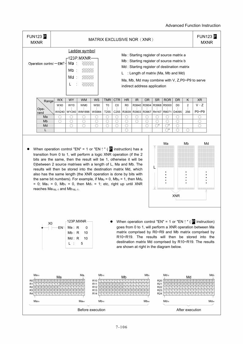
Advanced Function Instruction
7 -106
FUN123 P MXNR
MATRIX EXCLUSIVE NOR(XNR) FUN123 P
MXNR
Ma : Starting register of source matrix a Mb : Starting register of source matrix b Md : Starting register of destination matrix
L : Length of matrix (Ma, Mb and Md)
Ma, Mb, Md may combine with V, Z,P0~P9 to serve indirect address application
WX WY WM WS TMR CTR HR IR OR SR ROR DR K XR Range
Ope- rand
WX0 ∣
WX240
WY0∣
WY240
WM0 ∣
WM1896
WS0 ∣
WS984
T0∣
T255
C0∣
C255
R0 ∣
R3839
R3840∣
R3903
R3904∣
R3967
R3968∣
R4167
R5000∣
R8071
D0 ∣
D4095
2 ∣
256
V、Z
P0~P9Ma ○ ○ ○ ○ ○ ○ ○ ○ ○ ○ ○ ○ ○ Mb ○ ○ ○ ○ ○ ○ ○ ○ ○ ○ ○ ○ ○ Md ○ ○ ○ ○ ○ ○ ○ ○* ○* ○ ○ L ○ ○* ○ ○
When operation control "EN" = 1 or "EN↑" ( P instruction) has a transition from 0 to 1, will perform a logic XNR operation (if the 2 bits are the same, then the result will be 1, otherwise it will be 0)between 2 source matrixes with a length of L, Ma and Mb. The results will then be stored into the destination matrix Md, which also has the same length (the XNR operation is done by bits with the same bit numbers). For example, if Ma0 = 0, Mb0 = 1, then Md0 = 0; Ma1 = 0, Mb1 = 0, then Md1 = 1; etc, right up until XNR reaches Ma16L-1 and Mb16L-1.
L
Ma Mb Md
XNR
X0EN Ma :
Mb :R 10
L : 5
R 10R 0
Md :
123P.MXNR
When operation control "EN" = 1 or "EN↑" ( P instruction) goes from 0 to 1, will perform a XNR operation between Ma matrix comprised by R0~R9 and Mb matrix comprised by R10~R19. The results will then be stored into the destination matrix Md comprised by R10~R19. The results are shown at right in the diagram below.
Ma15 ↓ Ma Ma0
↓Mb15 ↓ Mb Mb0
↓Md15 ↓ Md Md0
↓R0 0 0 0 0 0 0 0 0 0 0 0 0 0 0 0 0 R10 1 1 1 1 1 1 1 1 1 1 1 1 1 1 1 1 R20 0 0 0 0 0 0 0 0 0 0 0 0 0 0 0 0R1 1 1 1 1 1 1 1 1 0 0 0 0 0 0 0 0 R11 0 0 0 0 0 0 0 0 1 1 1 1 1 1 1 1 R21 0 0 0 0 0 0 0 0 0 0 0 0 0 0 0 0R2 0 0 0 0 0 0 0 0 1 1 1 1 1 1 1 1 R12 0 0 0 0 0 0 0 0 1 1 1 1 1 1 1 1 R22 1 1 1 1 1 1 1 1 1 1 1 1 1 1 1 1R3 0 0 0 0 0 0 0 0 0 0 0 0 0 0 0 0 R13 0 0 0 0 0 0 0 0 0 0 0 0 0 0 0 0 R23 1 1 1 1 1 1 1 1 1 1 1 1 1 1 1 1R4 1 1 1 1 1 1 1 1 1 1 1 1 1 1 1 1 R14 1 1 1 1 1 1 1 1 1 1 1 1 1 1 1 1 R24 1 1 1 1 1 1 1 1 1 1 1 1 1 1 1 1
↑
Ma79
↑
Ma64
↑
Mb79
↑
Mb64
↑
Md79
↑
Md64
Before execution After execution
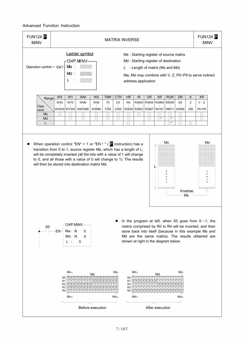
Advanced Function Instruction
7 -107
FUN124 P MINV
MATRIX INVERSE FUN124 P
MINV
Ms : Starting register of source matrix
Md : Starting register of destination
L : Length of matrix (Ms and Md)
Ma, Md may combine with V, Z, P0~P9 to serve indirect address application
WX WY WM WS TMR CTR HR IR OR SR ROR DR K XRRange
Ope- rand
WX0 ∣
WX240
WY0∣
WY240
WM0 ∣
WM1896
WS0 ∣
WS984
T0 ∣
T255
C0 ∣
C255
R0 ∣
R3839
R3840∣
R3903
R3904∣
R3967
R3968∣
R4167
R5000 ∣
R8071
D0 ∣
D4095
2 ∣
256
V、Z
P0~P9
Ms ○ ○ ○ ○ ○ ○ ○ ○ ○ ○ ○ ○ ○ Md ○ ○ ○ ○ ○ ○ ○ ○* ○* ○ ○ L ○ ○* ○ ○
When operation control "EN" = 1 or "EN↑" ( P instruction) has a transition from 0 to 1, source register Ms, which has a length of L, will be completely inverted (all the bits with a value of 1 will change to 0, and all those with a value of 0 will change to 1). The results will then be stored into destination matrix Md. L
MdMs
MsInverse
X0EN Ma :
124P.MINV
L : 5
R 0Md : R 0
In the program at left, when X0 goes from 0→1, the matrix comprised by R0 to R4 will be inverted, and then store back into itself (because in this example Ms and Md are the same matrix). The results obtained are shown at right in the diagram below.
Ms15 ↓ Ms
Ms0↓
Md15 ↓ Md
Md0↓
R0 0 0 0 0 0 0 0 0 0 0 0 0 0 0 0 0 R0 1 1 1 1 1 1 1 1 1 1 1 1 1 1 1 1 R1 1 1 1 1 1 1 1 1 0 0 0 0 0 0 0 0 R1 0 0 0 0 0 0 0 0 1 1 1 1 1 1 1 1 R2 0 0 0 0 0 0 0 0 1 1 1 1 1 1 1 1 R2 1 1 1 1 1 1 1 1 0 0 0 0 0 0 0 0 R3 0 0 0 0 0 0 0 0 0 0 0 0 0 0 0 0 R3 1 1 1 1 1 1 1 1 1 1 1 1 1 1 1 1 R4 1 1 1 1 1 1 1 1 1 1 1 1 1 1 1 1 R4 0 0 0 0 0 0 0 0 0 0 0 0 0 0 0 0
↑ Ms79
↑
Ms64
↑ Md79
↑
Md64
Before execution After execution
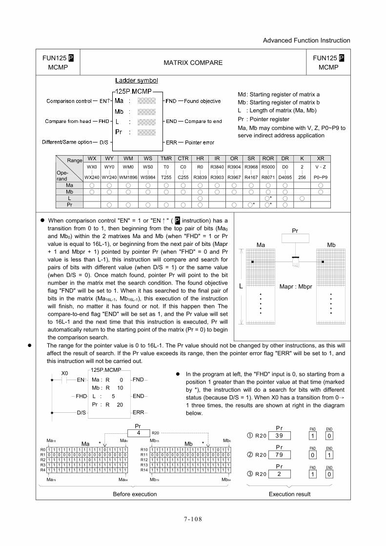
Advanced Function Instruction
7-108
FUN125 P MCMP
MATRIX COMPARE FUN125 P
MCMP
Md : Starting register of matrix a Mb : Starting register of matrix b L : Length of matrix (Ma, Mb) Pr : Pointer register Ma, Mb may combine with V, Z, P0~P9 to serve indirect address application
WX WY WM WS TMR CTR HR IR OR SR ROR DR K XR Range
Ope- rand
WX0 ∣
WX240
WY0∣
WY240
WM0 ∣
WM1896
WS0 ∣
WS984
T0 ∣
T255
C0 ∣
C255
R0 ∣
R3839
R3840∣
R3903
R3904∣
R3967
R3968∣
R4167
R5000 ∣
R8071
D0 ∣
D4095
2 ∣
256
V、Z
P0~P9
Ma ○ ○ ○ ○ ○ ○ ○ ○ ○ ○ ○ ○ ○ Mb ○ ○ ○ ○ ○ ○ ○ ○ ○ ○ ○ ○ ○ L ○ ○* ○ ○ Pr ○ ○ ○ ○ ○ ○ ○ ○* ○* ○
When comparison control "EN" = 1 or "EN↑" ( P instruction) has a transition from 0 to 1, then beginning from the top pair of bits (Ma0 and Mb0) within the 2 matrixes Ma and Mb (when "FHD" = 1 or Pr value is equal to 16L-1), or beginning from the next pair of bits (Mapr + 1 and Mbpr + 1) pointed by pointer Pr (when "FHD" = 0 and Pr value is less than L-1), this instruction will compare and search for pairs of bits with different value (when D/S = 1) or the same value (when D/S = 0). Once match found, pointer Pr will point to the bit number in the matrix met the search condition. The found objective flag "FND" will be set to 1. When it has searched to the final pair of bits in the matrix (Ma16L-1, Mb16L-1), this execution of the instruction will finish, no matter it has found or not. If this happen then The compare-to-end flag "END" will be set as 1, and the Pr value will set to 16L-1 and the next time that this instruction is executed, Pr will automatically return to the starting point of the matrix (Pr = 0) to begin the comparison search.
L
Ma Mb
Mapr : Mbpr
Pr
The range for the pointer value is 0 to 16L-1. The Pr value should not be changed by other instructions, as this will affect the result of search. If the Pr value exceeds its range, then the pointer error flag "ERR" will be set to 1, and this instruction will not be carried out.
X0EN
125P.MCMP
ENDL :Pr :
FHD
D/S ERR
5R 20
FNDMa :Mb : R 10
R 0
In the program at left, the "FHD" input is 0, so starting from a position 1 greater than the pointer value at that time (marked by *), the instruction will do a search for bits with different status (because D/S = 1). When X0 has a transition from 0→1 three times, the results are shown at right in the diagram below.
Pr 4 R20
Ma15 ↓ Ma * Ma0
↓ Mb15 ↓ Mb * Mb0
↓R0 1 1 1 1 1 1 1 1 1 1 1 0 1 1 1 1 R10 1 1 1 1 1 1 1 1 1 1 1 1 1 0 1 1R1 0 0 0 0 0 0 0 0 0 0 0 0 0 0 0 0 R11 0 0 0 0 0 0 0 0 0 0 0 0 0 0 0 0R2 1 1 1 1 1 1 1 1 0 1 1 1 1 1 1 1 R12 1 1 1 1 1 1 1 1 1 1 1 1 1 1 1 1R3 1 1 1 1 1 1 1 1 1 1 1 1 1 1 1 1 R13 1 1 1 1 1 1 1 1 1 1 1 1 1 1 1 1R4 1 1 1 1 1 1 1 1 1 1 1 1 1 1 1 1 R14 1 1 1 1 1 1 1 1 1 1 1 1 1 1 1 1
↑ Ma79
↑
Ma64 ↑ Mb79
↑
Mb64
Before execution
Pr
FND ENDR20 39 1 0
Pr
FND ENDR20 79 0 1
Pr
FND ENDR20 2 1 0
Execution result
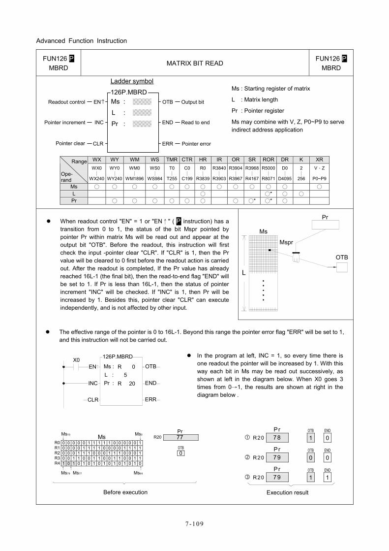
Advanced Function Instruction
7 -109
FUN126 P MBRD
MATRIX BIT READ FUN126 P
MBRD
Ms :ENReadout control
Ladder symbol
126P.MBRDOTB Output bit
END Read to endPointer increment INC
Pointer clear CLR
L :
Pr :
ERR Pointer error
Ms : Starting register of matrix
L : Matrix length
Pr : Pointer register
Ms may combine with V, Z, P0~P9 to serve indirect address application
WX WY WM WS TMR CTR HR IR OR SR ROR DR K XR Range
Ope- rand
WX0 ∣
WX240
WY0∣
WY240
WM0 ∣
WM1896
WS0 ∣
WS984
T0∣
T255
C0∣
C199
R0 ∣
R3839
R3840∣
R3903
R3904∣
R3967
R3968∣
R4167
R5000 ∣
R8071
D0 ∣
D4095
2 ∣
256
V、Z
P0~P9
Ms ○ ○ ○ ○ ○ ○ ○ ○ ○ ○ ○ ○ ○ L ○ ○* ○ ○ Pr ○ ○ ○ ○ ○ ○ ○ ○* ○* ○
When readout control "EN" = 1 or "EN↑" ( P instruction) has a transition from 0 to 1, the status of the bit Mspr pointed by pointer Pr within matrix Ms will be read out and appear at the output bit "OTB". Before the readout, this instruction will first check the input -pointer clear "CLR". If "CLR" is 1, then the Pr value will be cleared to 0 first before the readout action is carried out. After the readout is completed, If the Pr value has already reached 16L-1 (the final bit), then the read-to-end flag "END" will be set to 1. If Pr is less than 16L-1, then the status of pointer increment "INC" will be checked. If "INC" is 1, then Pr will be increased by 1. Besides this, pointer clear "CLR" can execute independently, and is not affected by other input.
L
Pr
Mspr
Ms
OTB
The effective range of the pointer is 0 to 16L-1. Beyond this range the pointer error flag "ERR" will be set to 1, and this instruction will not be carried out.
X0EN
126P.MBRD
ENDL :Pr :INC
CLR ERR
5R 20
OTBMs : R 0
In the program at left, INC = 1, so every time there is one readout the pointer will be increased by 1. With this way each bit in Ms may be read out successively, as shown at left in the diagram below. When X0 goes 3 times from 0→1, the results are shown at right in the diagram below .
Pr
Ms15 ↓ Ms Ms0
↓ R20 77R0 0 0 0 0 0 1 1 1 1 1 0 0 0 0 0 1 R1 0 0 0 0 1 1 1 1 0 0 0 0 1 1 1 1 OTB R2 0 0 0 1 1 1 0 0 0 1 1 1 0 0 0 1 0R3 0 0 1 1 0 0 1 1 0 0 1 1 0 0 1 1 R4 1 0 1 0 1 0 1 0 1 0 1 0 1 0 1 0
↑ ↑ Ms79 Ms77
↑
Ms64
Before execution
P r OTB END
R20 78 1 0
Pr OTB END
R20 79 0 0
Pr OTB END
R20 79 1 1
Execution result
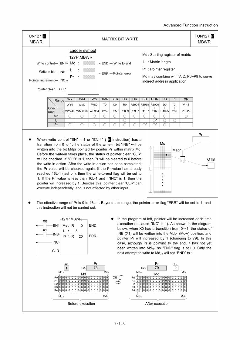
Advanced Function Instruction
7-110
FUN127 P MBWR
MATRIX BIT WRITE FUN127 P
MBWR
Md :ENWrite control
Ladder symbol
127P.MBWREND Write to end
Write-in bit INB
Pointer increment
CLR
L :
Pr :ERR Pointer error
INC
Pointer clear
Md : Starting register of matrix
L : Matrix length
Pr : Pointer register
Md may combine with V, Z, P0~P9 to serve indirect address application
WY WM WS TMR CTR HR OR SR ROR DR K XR Range
Ope- rand
WY0∣
WY240
WM0 ∣
WM1896
WS0 ∣
WS984
T0 ∣
T255
C0∣
C255
R0∣
R3839
R3904∣
R3967
R3968∣
R4167
R5000∣
R8071
D0∣
D4095
2 ∣
256
V、Z
P0~P9
Md ○ ○ ○ ○ ○ ○ ○ ○ ○ ○ ○ L ○ ○* ○ ○ Pr ○ ○ ○ ○ ○ ○ ○ ○* ○* ○
When write control "EN" = 1 or "EN↑" ( P instruction) has a transition from 0 to 1, the status of the write-in bit "INB" will be written into the bit Mdpr pointed by pointer Pr within matrix Md. Before the write-in takes place, the status of pointer clear "CLR" will be checked. If "CLR" is 1, then Pr will be cleared to 0 before the write-in action. After the write-in action has been completed, the Pr value will be checked again. If the Pr value has already reached 16L-1 (last bit), then the write-to-end flag will be set to 1. If the Pr value is less than 16L-1 and "INC" is 1, then the pointer will increased by 1. Besides this, pointer clear "CLR" can execute independently, and is not affected by other input.
L
Pr
Mspr
Ms
OTB
The effective range of Pr is 0 to 16L-1. Beyond this range, the pointer error flag "ERR" will be set to 1, and this instruction will not be carried out.
X0EN
127P.MBWR
ENDL :Pr :INB ERR
5R 20
Ms : R 0
INC
X1
CLR
In the program at left, pointer will be increased each time execution (because "INC" is 1). As shown in the diagram below, when X0 has a transition from 0→1, the status of INB (X1) will be written into the Mdpr (Md78) position, and pointer Pr will increased by 1 (changing to 79). In this case, although Pr is pointing to the end, it has not yet been written into Md79, so "END" flag is still 0. Only the next attempt to write to Md79 will set “END” to 1.
X1 Pr Pr EN
1 R20 78 R20 79 0
Md15 ↓ Md Md0
↓Md15 ↓ Md Md0
↓R0 0 0 0 0 0 0 0 0 0 0 0 0 0 0 0 0 R0 0 0 0 0 0 0 0 0 0 0 0 0 0 0 0 0 R1 0 0 0 0 0 0 0 0 0 0 0 0 0 0 0 0 R1 0 0 0 0 0 0 0 0 0 0 0 0 0 0 0 0 R2 0 0 0 0 0 0 0 0 0 0 0 0 0 0 0 0 R2 0 0 0 0 0 0 0 0 0 0 0 0 0 0 0 0 R3 0 0 0 0 0 0 0 0 0 0 0 0 0 0 0 0 R3 0 0 0 0 0 0 0 0 0 0 0 0 0 0 0 0 R4 0 0 0 0 0 0 0 0 0 0 0 0 0 0 0 0 R4 0 1 0 0 0 0 0 0 0 0 0 0 0 0 0 0
↑ Md79 ↑
Md64
X0=
↑ Md79
↑
Md64
Before execution After execution
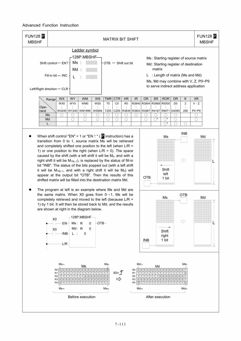
Advanced Function Instruction
7 -111
FUN128 P MBSHF
MATRIX BIT SHIFT FUN128 P
MBSHF
Ms :ENShift control
Ladder symbol
128P.MBSHFOTB Shift out bit
Fill-in bit INC
Left/Right direction CLR
L :
Md :
Ms : Starting register of source matrix
Md : Starting register of destination matrix
L : Length of matrix (Ms and Md)
Ms, Md may combine with V, Z, P0~P9 to serve indirect address application
WX WY WM WS TMR CTR HR IR OR SR ROR DR K XR Range
Ope- rand
WX0 ∣
WX240
WY0 ∣
WY240
WM0 ∣
WM1896
WS0∣
WS984
T0∣
T255
C0∣
C255
R0∣
R3839
R3840∣
R3903
R3904∣
R3967
R3968∣
R4167
R5000∣
R8071
D0 ∣
D4095
2 ∣
256
V、Z
P0~P9Ms ○ ○ ○ ○ ○ ○ ○ ○ ○ ○ ○ ○ ○ Md ○ ○ ○ ○ ○ ○ ○ ○* ○* ○ ○ L ○* ○ ○
Ms
Shiftleft
1 bitOTB
INBMd
L
When shift control "EN" = 1 or "EN↑" ( P instruction) has a transition from 0 to 1, source matrix Ms will be retrieved and completely shifted one position to the left (when L/R = 1) or one position to the right (when L/R = 0). The space caused by the shift (with a left shift it will be M0, and with a right shift it will be M16L-1), is replaced by the status of fill-in bit "INB". The status of the bits popped out (with a left shift it will be M16L-1, and with a right shift it will be M0) will appear at the output bit "OTB". Then the results of this shifted matrix will be filled into the destination matrix Md.
The program at left is an example where Ms and Md are the same matrix. When X0 goes from 0→1, Ms will be completely retrieved and moved to the left (because L/R = 1) by 1 bit. It will then be stored back to Md, and the results are shown at right in the diagram below.
X0EN
128P.MBSHF
L :Md :
INB
L/R
5
OTBMs : R 0R 0X0
L
Ms MdOTB
INB
Shiftright1 bit
Ms15 ↓ Ms Ms0
↓Md15 ↓ Md
Md0
↓R0 0 0 0 0 0 0 0 0 0 0 0 0 0 0 0 0 R0 0 0 0 0 0 0 0 0 0 0 0 0 0 0 0 1 R1 1 1 1 1 1 1 1 1 1 1 1 1 1 1 1 1 R1 1 1 1 1 1 1 1 1 1 1 1 1 1 1 1 0 R2 1 1 1 1 1 1 1 1 0 0 0 0 0 0 0 0 R2 1 1 1 1 1 1 1 0 0 0 0 0 0 0 0 1 R3 0 0 0 0 0 0 0 0 0 0 0 0 0 0 0 0 R3 0 0 0 0 0 0 0 0 0 0 0 0 0 0 0 1 R4 0 1 1 1 1 1 1 1 1 1 1 1 1 1 1 1 R4 1 1 1 1 1 1 1 1 1 1 1 1 1 1 1 0
↑ Ms79 ↑
Ms64
X0=
↑ Md79
↑
Md64
Before execution After execution
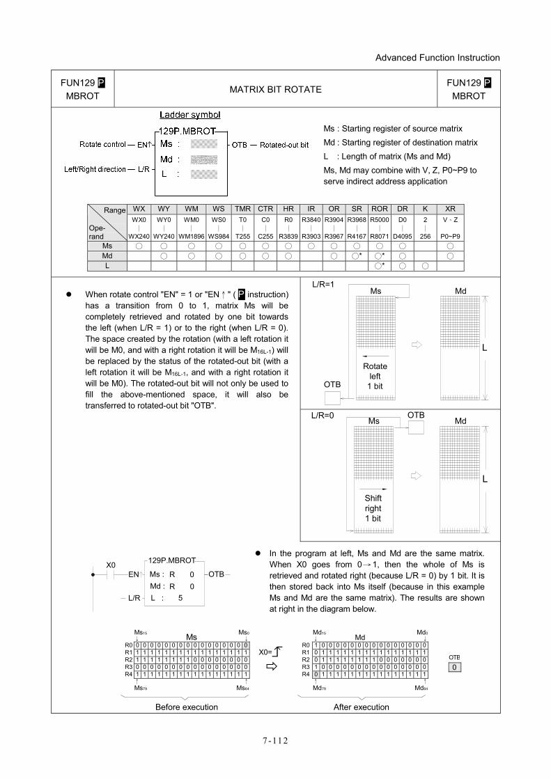
Advanced Function Instruction
7-112
FUN129 P MBROT
MATRIX BIT ROTATE FUN129 P
MBROT
Ms : Starting register of source matrix Md : Starting register of destination matrix L : Length of matrix (Ms and Md) Ms, Md may combine with V, Z, P0~P9 to serve indirect address application
WX WY WM WS TMR CTR HR IR OR SR ROR DR K XRRange
Ope- rand
WX0 ∣
WX240
WY0 ∣
WY240
WM0 ∣
WM1896
WS0 ∣
WS984
T0 ∣
T255
C0∣
C255
R0∣
R3839
R3840∣
R3903
R3904∣
R3967
R3968∣
R4167
R5000∣
R8071
D0 ∣
D4095
2 ∣
256
V、Z
P0~P9Ms ○ ○ ○ ○ ○ ○ ○ ○ ○ ○ ○ ○ ○ Md ○ ○ ○ ○ ○ ○ ○ ○* ○* ○ ○ L ○* ○ ○
L
Ms Md
Rotateleft
1 bitOTB
L/R=1 When rotate control "EN" = 1 or "EN↑" ( P instruction)
has a transition from 0 to 1, matrix Ms will be completely retrieved and rotated by one bit towards the left (when L/R = 1) or to the right (when L/R = 0). The space created by the rotation (with a left rotation it will be M0, and with a right rotation it will be M16L-1) will be replaced by the status of the rotated-out bit (with a left rotation it will be M16L-1, and with a right rotation it will be M0). The rotated-out bit will not only be used to fill the above-mentioned space, it will also be transferred to rotated-out bit "OTB".
L
Ms Md
Shiftright1 bit
OTBL/R=0
X0EN
129P.MBROT
L :Md :
L/R 5
OTBMs : R 0R 0
In the program at left, Ms and Md are the same matrix. When X0 goes from 0→1, then the whole of Ms is retrieved and rotated right (because L/R = 0) by 1 bit. It is then stored back into Ms itself (because in this example Ms and Md are the same matrix). The results are shown at right in the diagram below.
Ms15 ↓ Ms Ms0
↓Md15 ↓ Md
Md0
↓R0 0 0 0 0 0 0 0 0 0 0 0 0 0 0 0 0 R0 1 0 0 0 0 0 0 0 0 0 0 0 0 0 0 0 R1 1 1 1 1 1 1 1 1 1 1 1 1 1 1 1 1 R1 0 1 1 1 1 1 1 1 1 1 1 1 1 1 1 1 R2 1 1 1 1 1 1 1 1 0 0 0 0 0 0 0 0 R2 0 1 1 1 1 1 1 1 1 0 0 0 0 0 0 0 R3 0 0 0 0 0 0 0 0 0 0 0 0 0 0 0 0 R3 1 0 0 0 0 0 0 0 0 0 0 0 0 0 0 0 R4 1 1 1 1 1 1 1 1 1 1 1 1 1 1 1 1 R4 0 1 1 1 1 1 1 1 1 1 1 1 1 1 1 1
↑ Ms79 ↑
Ms64
X0=
↑ Md79
↑
Md64
Before execution After execution
OTB
0
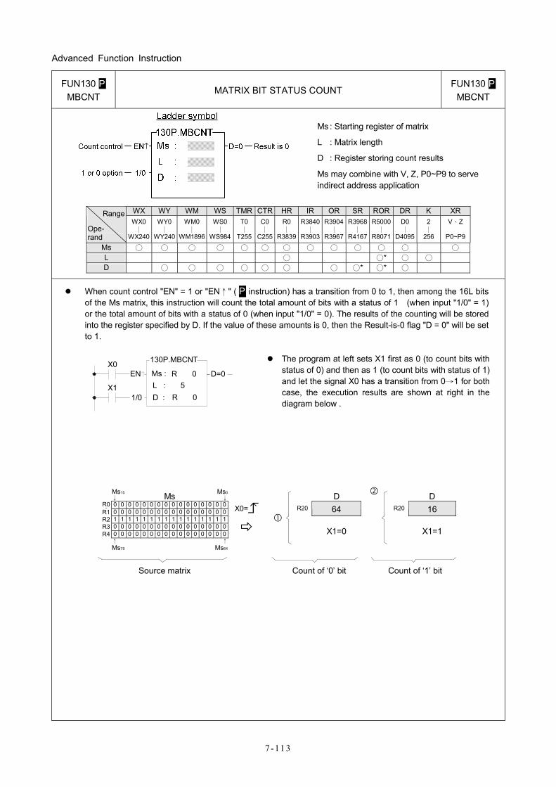
Advanced Function Instruction
7 -113
FUN130 P MBCNT
MATRIX BIT STATUS COUNT FUN130 P
MBCNT
Ms : Starting register of matrix
L : Matrix length
D : Register storing count results
Ms may combine with V, Z, P0~P9 to serve indirect address application
WX WY WM WS TMR CTR HR IR OR SR ROR DR K XR Range
Ope- rand
WX0 ∣
WX240
WY0∣
WY240
WM0 ∣
WM1896
WS0 ∣
WS984
T0∣
T255
C0∣
C255
R0 ∣
R3839
R3840∣
R3903
R3904∣
R3967
R3968∣
R4167
R5000∣
R8071
D0 ∣
D4095
2 ∣
256
V、Z
P0~P9
Ms ○ ○ ○ ○ ○ ○ ○ ○ ○ ○ ○ ○ ○ L ○ ○* ○ ○ D ○ ○ ○ ○ ○ ○ ○ ○* ○* ○
When count control "EN" = 1 or "EN↑" ( P instruction) has a transition from 0 to 1, then among the 16L bits of the Ms matrix, this instruction will count the total amount of bits with a status of 1 (when input "1/0" = 1) or the total amount of bits with a status of 0 (when input "1/0" = 0). The results of the counting will be stored into the register specified by D. If the value of these amounts is 0, then the Result-is-0 flag "D = 0" will be set to 1.
X0EN
130P.MBCNT
D :
Ms : R 0
X1 L : 5R 0
D=0
1/0
The program at left sets X1 first as 0 (to count bits with status of 0) and then as 1 (to count bits with status of 1) and let the signal X0 has a transition from 0→1 for both case, the execution results are shown at right in the diagram below .
Ms15 ↓ Ms Ms0
↓ D D R00
0 0 0 0 0 0 0 0 0 0 0 0 0 0 0 0 R1 0 0 0 0 0 0 0 0 0 0 0 0 0 0 0 0 R20 64 R20 16 R2 1 1 1 1 1 1 1 1 1 1 1 1 1 1 1 1 R3 0 0 0 0 0 0 0 0 0 0 0 0 0 0 0 0 R4 0 0 0 0 0 0 0 0 0 0 0 0 0 0 0 0 X1=0 X1=1
↑ Ms79 ↑
Ms64
X0=
Source matrix Count of ‘0’ bit Count of ‘1’ bit
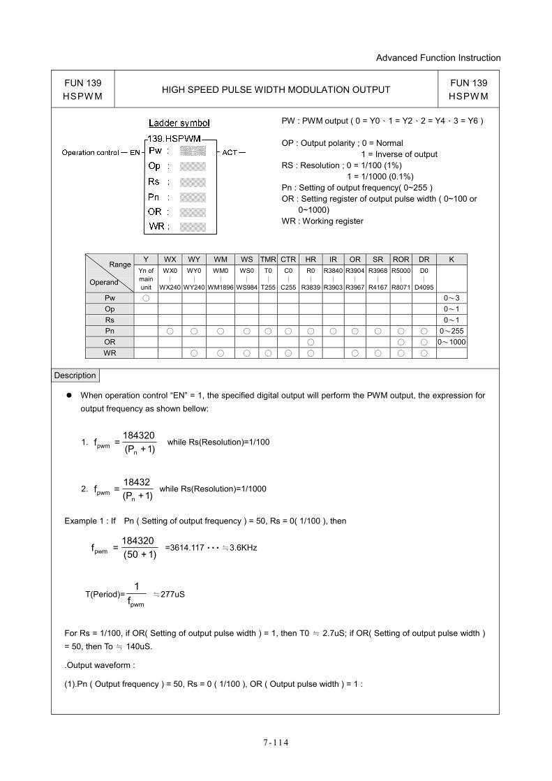
Advanced Function Instruction
7 -114
FUN 139 HSPW M
HIGH SPEED PULSE WIDTH MODULATION OUTPUT FUN 139 HSPW M
PW : PWM output ( 0 = Y0、1 = Y2、2 = Y4、3 = Y6 ) OP : Output polarity ; 0 = Normal 1 = Inverse of output RS : Resolution ; 0 = 1/100 (1%) 1 = 1/1000 (0.1%) Pn : Setting of output frequency( 0~255 ) OR : Setting register of output pulse width ( 0~100 or
0~1000) WR : Working register
Y WX WY WM WS TMR CTR HR IR OR SR ROR DR K
Range Operand
Yn of main unit
WX0 ∣
WX240
WY0 ∣
WY240
WM0∣
WM1896
WS0∣
WS984
T0∣
T255
C0∣
C255
R0 ∣
R3839
R3840∣
R3903
R3904∣
R3967
R3968∣
R4167
R5000 ∣
R8071
D0 ∣
D4095
Pw ○ 0~3Op 0~1Rs 0~1Pn ○ ○ ○ ○ ○ ○ ○ ○ ○ ○ ○ ○ 0~255OR ○ ○ ○ 0~1000WR ○ ○ ○ ○ ○ ○ ○ ○ ○ ○
Description
When operation control “EN” = 1, the specified digital output will perform the PWM output, the expression for output frequency as shown bellow:
1. )1+P(
184320=f
npwm while Rs(Resolution)=1/100
2. )1+P(
18432=f
npwm while Rs(Resolution)=1/1000
Example 1 : If Pn ( Setting of output frequency ) = 50, Rs = 0( 1/100 ), then
)1+50(184320
=fpwm =3614.117‧‧‧ ≒3.6KHz
T(Period)=pwmf1
≒277uS
For Rs = 1/100, if OR( Setting of output pulse width ) = 1, then T0 2.7≒ uS; if OR( Setting of output pulse width ) = 50, then To ≒ 140uS.
.Output waveform :
(1).Pn ( Output frequency ) = 50, Rs = 0 ( 1/100 ), OR ( Output pulse width ) = 1 :
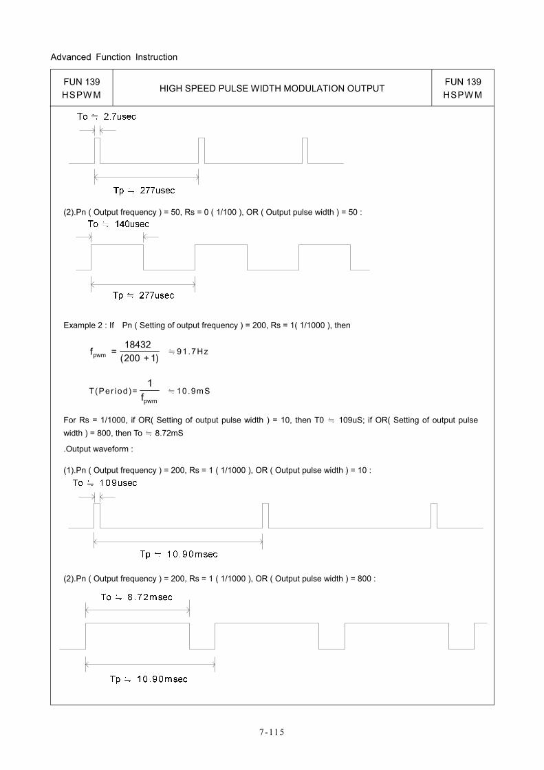
Advanced Function Instruction
7 -115
FUN 139 HSPW M
HIGH SPEED PULSE WIDTH MODULATION OUTPUT FUN 139 HSPW M
(2).Pn ( Output frequency ) = 50, Rs = 0 ( 1/100 ), OR ( Output pulse width ) = 50 :
Example 2 : If Pn ( Setting of output frequency ) = 200, Rs = 1( 1/1000 ), then
)1+200(18432
=fpwm 91 .7Hz≒
T(Per iod)=pwmf1
10 .9mS≒
For Rs = 1/1000, if OR( Setting of output pulse width ) = 10, then T0 ≒ 109uS; if OR( Setting of output pulse width ) = 800, then To ≒ 8.72mS
.Output waveform :
(1).Pn ( Output frequency ) = 200, Rs = 1 ( 1/1000 ), OR ( Output pulse width ) = 10 :
(2).Pn ( Output frequency ) = 200, Rs = 1 ( 1/1000 ), OR ( Output pulse width ) = 800 :
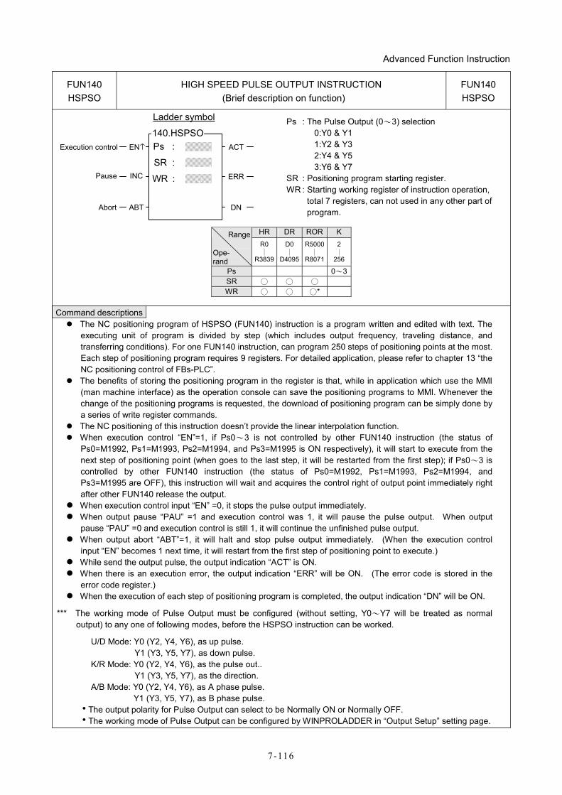
Advanced Function Instruction
7-116
FUN140 HSPSO
HIGH SPEED PULSE OUTPUT INSTRUCTION (Brief description on function)
FUN140 HSPSO
Ps :ENExecution control
Ladder symbol
140.HSPSOACT
ERRPause INC
Abort ABT
SR :
WR :
DN
Ps : The Pulse Output (0~3) selection 0:Y0 & Y1 1:Y2 & Y3 2:Y4 & Y5 3:Y6 & Y7
SR : Positioning program starting register. WR : Starting working register of instruction operation,
total 7 registers, can not used in any other part of program.
HR DR ROR K Range
Ope- rand
R0 ∣
R3839
D0 ∣
D4095
R5000∣
R8071
2 ∣
256
Ps 0~3SR ○ ○ ○ WR ○ ○ ○*
Command descriptions
The NC positioning program of HSPSO (FUN140) instruction is a program written and edited with text. The executing unit of program is divided by step (which includes output frequency, traveling distance, and transferring conditions). For one FUN140 instruction, can program 250 steps of positioning points at the most. Each step of positioning program requires 9 registers. For detailed application, please refer to chapter 13 “the NC positioning control of FBs-PLC”.
The benefits of storing the positioning program in the register is that, while in application which use the MMI (man machine interface) as the operation console can save the positioning programs to MMI. Whenever the change of the positioning programs is requested, the download of positioning program can be simply done by a series of write register commands.
The NC positioning of this instruction doesn’t provide the linear interpolation function. When execution control “EN”=1, if Ps0~3 is not controlled by other FUN140 instruction (the status of
Ps0=M1992, Ps1=M1993, Ps2=M1994, and Ps3=M1995 is ON respectively), it will start to execute from the next step of positioning point (when goes to the last step, it will be restarted from the first step); if Ps0~3 is controlled by other FUN140 instruction (the status of Ps0=M1992, Ps1=M1993, Ps2=M1994, and Ps3=M1995 are OFF), this instruction will wait and acquires the control right of output point immediately right after other FUN140 release the output.
When execution control input “EN” =0, it stops the pulse output immediately. When output pause “PAU” =1 and execution control was 1, it will pause the pulse output. When output
pause “PAU” =0 and execution control is still 1, it will continue the unfinished pulse output. When output abort “ABT”=1, it will halt and stop pulse output immediately. (When the execution control
input “EN” becomes 1 next time, it will restart from the first step of positioning point to execute.) While send the output pulse, the output indication “ACT” is ON. When there is an execution error, the output indication “ERR” will be ON. (The error code is stored in the
error code register.) When the execution of each step of positioning program is completed, the output indication “DN” will be ON.
*** The working mode of Pulse Output must be configured (without setting, Y0~Y7 will be treated as normal output) to any one of following modes, before the HSPSO instruction can be worked.
U/D Mode: Y0 (Y2, Y4, Y6), as up pulse. Y1 (Y3, Y5, Y7), as down pulse.
K/R Mode: Y0 (Y2, Y4, Y6), as the pulse out.. Y1 (Y3, Y5, Y7), as the direction.
A/B Mode: Y0 (Y2, Y4, Y6), as A phase pulse. Y1 (Y3, Y5, Y7), as B phase pulse.
hThe output polarity for Pulse Output can select to be Normally ON or Normally OFF. hThe working mode of Pulse Output can be configured by WINPROLADDER in “Output Setup” setting page.
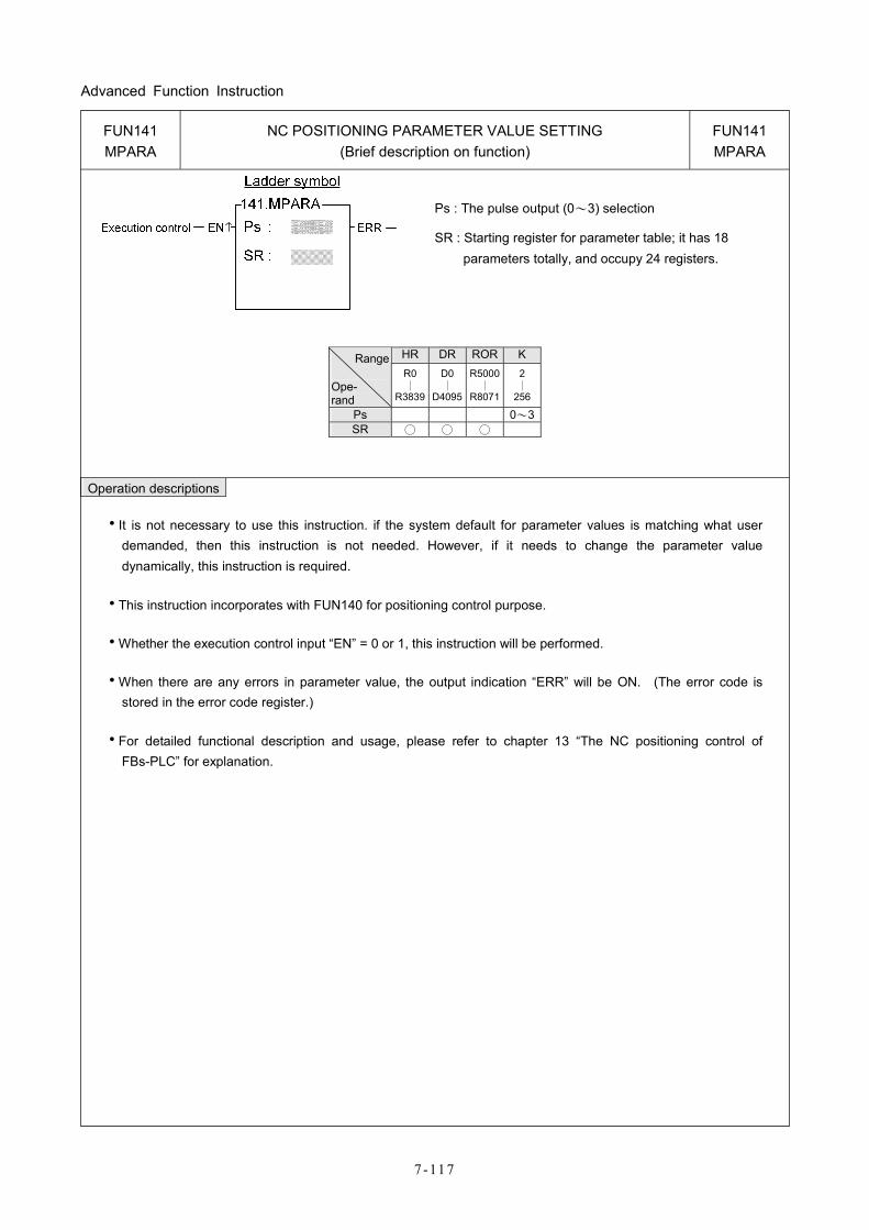
Advanced Function Instruction
7 -117
FUN141 MPARA
NC POSITIONING PARAMETER VALUE SETTING (Brief description on function)
FUN141 MPARA
Ps : The pulse output (0~3) selection
SR : Starting register for parameter table; it has 18 parameters totally, and occupy 24 registers.
HR DR ROR K Range
Ope- rand
R0 ∣
R3839
D0 ∣
D4095
R5000∣
R8071
2 ∣
256
Ps 0~3SR ○ ○ ○
Operation descriptions
hIt is not necessary to use this instruction. if the system default for parameter values is matching what user demanded, then this instruction is not needed. However, if it needs to change the parameter value dynamically, this instruction is required.
hThis instruction incorporates with FUN140 for positioning control purpose.
hWhether the execution control input “EN” = 0 or 1, this instruction will be performed.
hWhen there are any errors in parameter value, the output indication “ERR” will be ON. (The error code is stored in the error code register.)
hFor detailed functional description and usage, please refer to chapter 13 “The NC positioning control of FBs-PLC” for explanation.
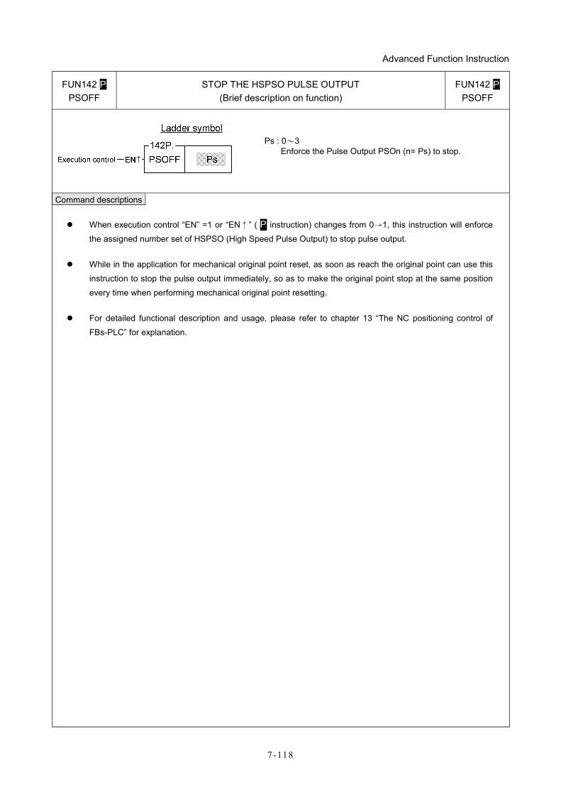
Advanced Function Instruction
7-118
FUN142 P PSOFF
STOP THE HSPSO PULSE OUTPUT (Brief description on function)
FUN142 P PSOFF
Ps : 0~3 Enforce the Pulse Output PSOn (n= Ps) to stop.
Command descriptions
When execution control “EN” =1 or “EN↑” ( P instruction) changes from 0→1, this instruction will enforce
the assigned number set of HSPSO (High Speed Pulse Output) to stop pulse output.
While in the application for mechanical original point reset, as soon as reach the original point can use this
instruction to stop the pulse output immediately, so as to make the original point stop at the same position
every time when performing mechanical original point resetting.
For detailed functional description and usage, please refer to chapter 13 “The NC positioning control of
FBs-PLC” for explanation.
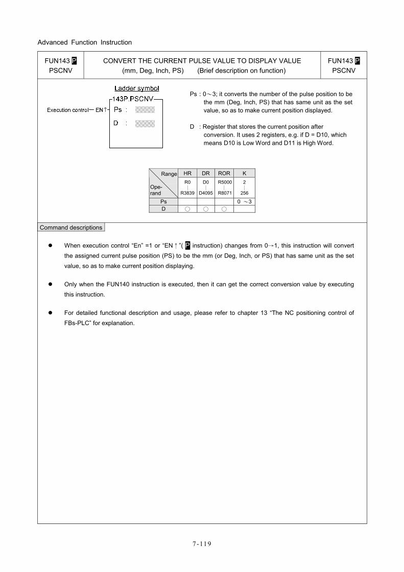
Advanced Function Instruction
7 -119
FUN143 P PSCNV
CONVERT THE CURRENT PULSE VALUE TO DISPLAY VALUE (mm, Deg, Inch, PS) (Brief description on function)
FUN143 P PSCNV
Ps : 0~3; it converts the number of the pulse position to be the mm (Deg, Inch, PS) that has same unit as the set value, so as to make current position displayed.
D : Register that stores the current position after conversion. It uses 2 registers, e.g. if D = D10, which means D10 is Low Word and D11 is High Word.
HR DR ROR K Range
Ope- rand
R0 ∣
R3839
D0 ∣
D4095
R5000∣
R8071
2 ∣
256
Ps 0 ~3D ○ ○ ○
Command descriptions
When execution control “En” =1 or “EN↑”( P instruction) changes from 0→1, this instruction will convert
the assigned current pulse position (PS) to be the mm (or Deg, Inch, or PS) that has same unit as the set
value, so as to make current position displaying.
Only when the FUN140 instruction is executed, then it can get the correct conversion value by executing
this instruction.
For detailed functional description and usage, please refer to chapter 13 “The NC positioning control of
FBs-PLC” for explanation.
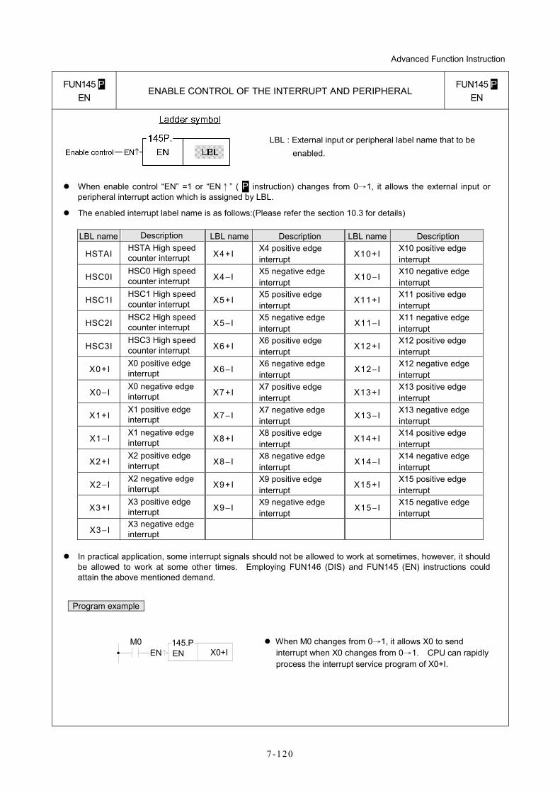
Advanced Function Instruction
7 -120
FUN145 P EN
ENABLE CONTROL OF THE INTERRUPT AND PERIPHERAL FUN145 P
EN
LBL : External input or peripheral label name that to be enabled.
When enable control “EN” =1 or “EN↑” ( P instruction) changes from 0→1, it allows the external input or peripheral interrupt action which is assigned by LBL.
The enabled interrupt label name is as follows:(Please refer the section 10.3 for details)
LBL name Description LBL name Description LBL name Description
HSTAI HSTA High speed counter interrupt X4+I
X4 positive edge interrupt
X10+I X10 positive edge interrupt
HSC0I HSC0 High speed counter interrupt X4− I
X5 negative edge interrupt
X10− I X10 negative edge interrupt
HSC1I HSC1 High speed counter interrupt X5+I
X5 positive edge interrupt
X11+I X11 positive edge interrupt
HSC2I HSC2 High speed counter interrupt X5− I
X5 negative edge interrupt
X11− I X11 negative edge interrupt
HSC3I HSC3 High speed counter interrupt X6+I
X6 positive edge interrupt
X12+I X12 positive edge interrupt
X0+I X0 positive edge interrupt X6− I
X6 negative edge interrupt
X12− I X12 negative edge interrupt
X0− I X0 negative edge interrupt X7+I
X7 positive edge interrupt
X13+I X13 positive edge interrupt
X1+I X1 positive edge interrupt X7− I
X7 negative edge interrupt
X13− I X13 negative edge interrupt
X1− I X1 negative edge interrupt X8+I
X8 positive edge interrupt
X14+I X14 positive edge interrupt
X2+I X2 positive edge interrupt X8− I
X8 negative edge interrupt
X14− I X14 negative edge interrupt
X2− I X2 negative edge interrupt X9+I
X9 positive edge interrupt
X15+I X15 positive edge interrupt
X3+I X3 positive edge interrupt X9− I
X9 negative edge interrupt
X15− I X15 negative edge interrupt
X3− I X3 negative edge interrupt
In practical application, some interrupt signals should not be allowed to work at sometimes, however, it should be allowed to work at some other times. Employing FUN146 (DIS) and FUN145 (EN) instructions could attain the above mentioned demand.
Program example
EN145.PM0EN X0+I
When M0 changes from 0→1, it allows X0 to send interrupt when X0 changes from 0→1. CPU can rapidly process the interrupt service program of X0+I.
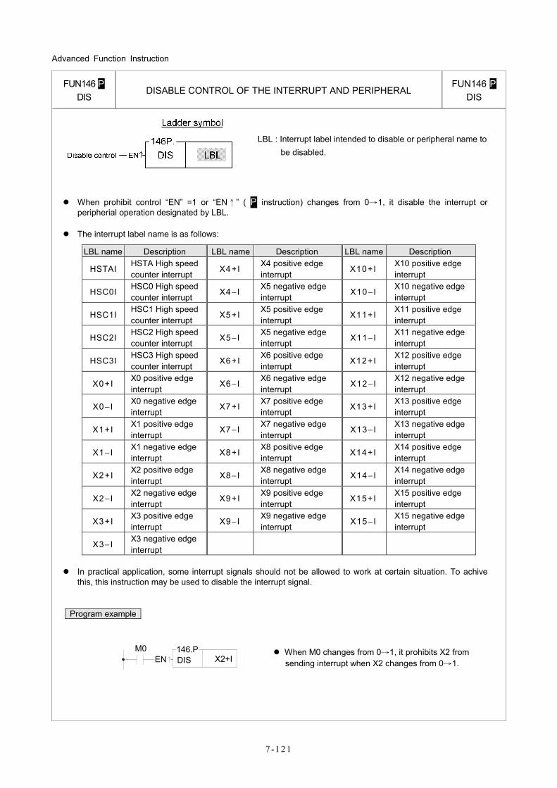
Advanced Function Instruction
7 -121
FUN146 P DIS
DISABLE CONTROL OF THE INTERRUPT AND PERIPHERAL FUN146 P
DIS
LBL : Interrupt label intended to disable or peripheral name to be disabled.
When prohibit control “EN” =1 or “EN↑” ( P instruction) changes from 0→1, it disable the interrupt or peripherial operation designated by LBL.
The interrupt label name is as follows:
LBL name Description LBL name Description LBL name Description
HSTAI HSTA High speed counter interrupt
X4+I X4 positive edge interrupt
X10+I X10 positive edge interrupt
HSC0I HSC0 High speed counter interrupt
X4− I X5 negative edge interrupt
X10− I X10 negative edge interrupt
HSC1I HSC1 High speed counter interrupt
X5+I X5 positive edge interrupt
X11+I X11 positive edge interrupt
HSC2I HSC2 High speed counter interrupt
X5− I X5 negative edge interrupt
X11− I X11 negative edge interrupt
HSC3I HSC3 High speed counter interrupt
X6+I X6 positive edge interrupt
X12+I X12 positive edge interrupt
X0+I X0 positive edge interrupt
X6− I X6 negative edge interrupt
X12− I X12 negative edge interrupt
X0− I X0 negative edge interrupt
X7+I X7 positive edge interrupt
X13+I X13 positive edge interrupt
X1+I X1 positive edge interrupt
X7− I X7 negative edge interrupt
X13− I X13 negative edge interrupt
X1− I X1 negative edge interrupt
X8+I X8 positive edge interrupt
X14+I X14 positive edge interrupt
X2+I X2 positive edge interrupt
X8− I X8 negative edge interrupt
X14− I X14 negative edge interrupt
X2− I X2 negative edge interrupt
X9+I X9 positive edge interrupt
X15+I X15 positive edge interrupt
X3+I X3 positive edge interrupt
X9− I X9 negative edge interrupt
X15− I X15 negative edge interrupt
X3− I X3 negative edge interrupt
In practical application, some interrupt signals should not be allowed to work at certain situation. To achive this, this instruction may be used to disable the interrupt signal.
Program example
M0EN
146.PDIS X2+I
When M0 changes from 0→1, it prohibits X2 from sending interrupt when X2 changes from 0→1.
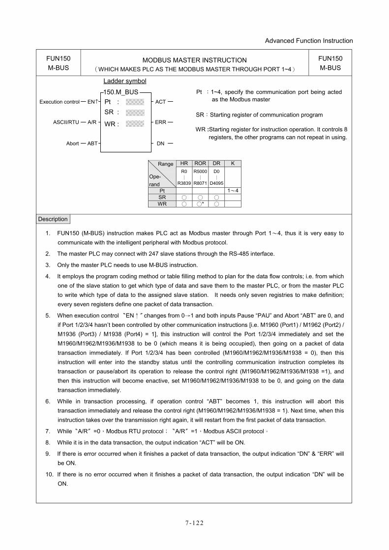
Advanced Function Instruction
7 -122
FUN150 M-BUS
MODBUS MASTER INSTRUCTION (WHICH MAKES PLC AS THE MODBUS MASTER THROUGH PORT 1~4)
FUN150 M-BUS
Pt :ENExecution control
Ladder symbol
150.M_BUSACT
ERRASCII/RTU A/R
Abort ABT
SR :
DN
WR :
Pt :1~4, specify the communication port being acted as the Modbus master
SR:Starting register of communication program
WR :Starting register for instruction operation. It controls 8 registers, the other programs can not repeat in using.
HR ROR DR KRange
Ope- rand
R0 ∣
R3839
R5000∣
R8071
D0∣
D4095
Pt 1~4SR ○ ○ ○ WR ○ ○* ○
Description
1. FUN150 (M-BUS) instruction makes PLC act as Modbus master through Port 1~4, thus it is very easy to communicate with the intelligent peripheral with Modbus protocol.
2. The master PLC may connect with 247 slave stations through the RS-485 interface.
3. Only the master PLC needs to use M-BUS instruction.
4. It employs the program coding method or table filling method to plan for the data flow controls; i.e. from which one of the slave station to get which type of data and save them to the master PLC, or from the master PLC to write which type of data to the assigned slave station. It needs only seven registries to make definition; every seven registers define one packet of data transaction.
5. When execution control 〝EN↑〞changes from 0→1 and both inputs Pause “PAU” and Abort “ABT” are 0, and if Port 1/2/3/4 hasn’t been controlled by other communication instructions [i.e. M1960 (Port1) / M1962 (Port2) / M1936 (Port3) / M1938 (Port4) = 1], this instruction will control the Port 1/2/3/4 immediately and set the M1960/M1962/M1936/M1938 to be 0 (which means it is being occupied), then going on a packet of data transaction immediately. If Port 1/2/3/4 has been controlled (M1960/M1962/M1936/M1938 = 0), then this instruction will enter into the standby status until the controlling communication instruction completes its transaction or pause/abort its operation to release the control right (M1960/M1962/M1936/M1938 =1), and then this instruction will become enactive, set M1960/M1962/M1936/M1938 to be 0, and going on the data transaction immediately.
6. While in transaction processing, if operation control “ABT” becomes 1, this instruction will abort this transaction immediately and release the control right (M1960/M1962/M1936/M1938 = 1). Next time, when this instruction takes over the transmission right again, it will restart from the first packet of data transaction.
7. While〝A/R〞=0,Modbus RTU protocol;〝A/R〞=1,Modbus ASCII protocol。
8. While it is in the data transaction, the output indication “ACT” will be ON.
9. If there is error occurred when it finishes a packet of data transaction, the output indication “DN” & “ERR” will be ON.
10. If there is no error occurred when it finishes a packet of data transaction, the output indication “DN” will be ON.
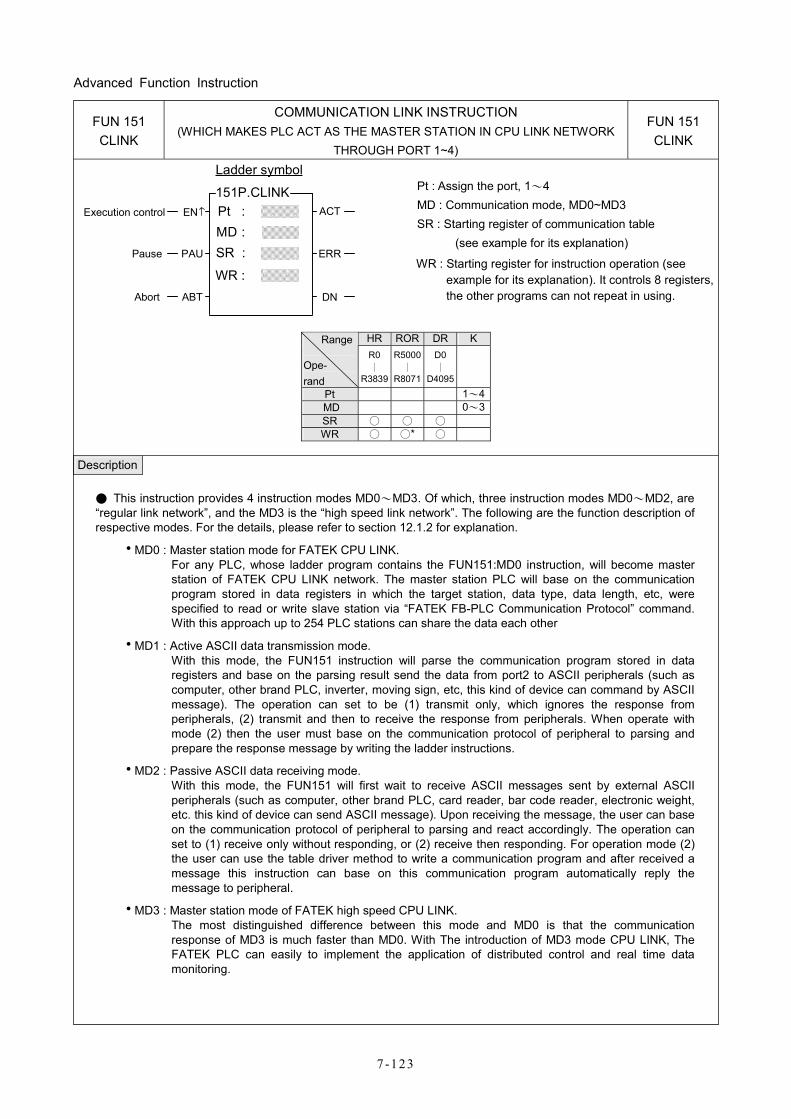
Advanced Function Instruction
7 -123
FUN 151 CLINK
COMMUNICATION LINK INSTRUCTION (WHICH MAKES PLC ACT AS THE MASTER STATION IN CPU LINK NETWORK
THROUGH PORT 1~4)
FUN 151 CLINK
Pt :ENExecution control
Ladder symbol
151P.CLINKACT
ERRPause PAU
Abort ABT
SR :
DN
WR :
MD :
Pt : Assign the port, 1~4 MD : Communication mode, MD0~MD3 SR : Starting register of communication table
(see example for its explanation)
WR : Starting register for instruction operation (see example for its explanation). It controls 8 registers, the other programs can not repeat in using.
HR ROR DR KRange
Ope- rand
R0 ∣
R3839
R5000∣
R8071
D0∣
D4095
Pt 1~4 MD 0~3
SR ○ ○ ○ WR ○ ○* ○
Description
● This instruction provides 4 instruction modes MD0~MD3. Of which, three instruction modes MD0~MD2, are “regular link network”, and the MD3 is the “high speed link network”. The following are the function description of respective modes. For the details, please refer to section 12.1.2 for explanation.
hMD0 : Master station mode for FATEK CPU LINK. For any PLC, whose ladder program contains the FUN151:MD0 instruction, will become master station of FATEK CPU LINK network. The master station PLC will base on the communication program stored in data registers in which the target station, data type, data length, etc, were specified to read or write slave station via “FATEK FB-PLC Communication Protocol” command. With this approach up to 254 PLC stations can share the data each other
hMD1 : Active ASCII data transmission mode. With this mode, the FUN151 instruction will parse the communication program stored in data registers and base on the parsing result send the data from port2 to ASCII peripherals (such as computer, other brand PLC, inverter, moving sign, etc, this kind of device can command by ASCII message). The operation can set to be (1) transmit only, which ignores the response from peripherals, (2) transmit and then to receive the response from peripherals. When operate with mode (2) then the user must base on the communication protocol of peripheral to parsing and prepare the response message by writing the ladder instructions.
hMD2 : Passive ASCII data receiving mode. With this mode, the FUN151 will first wait to receive ASCII messages sent by external ASCII peripherals (such as computer, other brand PLC, card reader, bar code reader, electronic weight, etc. this kind of device can send ASCII message). Upon receiving the message, the user can base on the communication protocol of peripheral to parsing and react accordingly. The operation can set to (1) receive only without responding, or (2) receive then responding. For operation mode (2) the user can use the table driver method to write a communication program and after received a message this instruction can base on this communication program automatically reply the message to peripheral.
hMD3 : Master station mode of FATEK high speed CPU LINK. The most distinguished difference between this mode and MD0 is that the communication response of MD3 is much faster than MD0. With The introduction of MD3 mode CPU LINK, The FATEK PLC can easily to implement the application of distributed control and real time data monitoring.
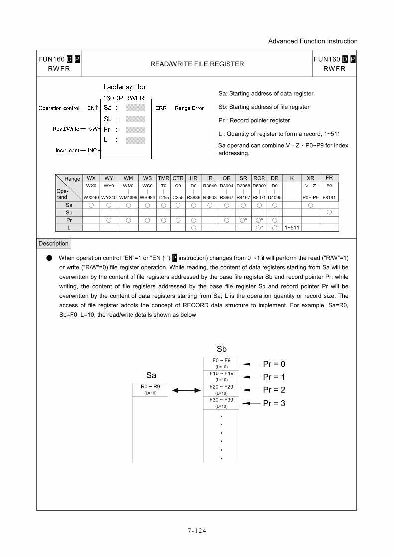
Advanced Function Instruction
7 -124
FUN160 D P RW FR
READ/WRITE FILE REGISTER FUN160 D P
RW FR
Sa: Starting address of data register
Sb: Starting address of file register
Pr : Record pointer register
L : Quantity of register to form a record, 1~511
Sa operand can combine V、Z、P0~P9 for index addressing.
WX WY WM WS TMR CTR HR IR OR SR ROR DR K XR FR Range
Ope- rand
WX0 ∣
WX240
WY0 ∣
WY240
WM0 ∣
WM1896
WS0 ∣
WS984
T0∣
T255
C0∣
C255
R0∣
R3839
R3840∣
R3903
R3904∣
R3967
R3968∣
R4167
R5000∣
R8071
D0∣
D4095
V、Z
P0~P9
F0 ∣
F8191Sa ○ ○ ○ ○ ○ ○ ○ ○ ○ ○ ○ ○ ○ Sb ○ Pr ○ ○ ○ ○ ○ ○ ○ ○* ○* ○ L ○ ○* ○ 1~511
Description
● When operation control "EN"=1 or "EN↑"( P instruction) changes from 0→1,it will perform the read ("R/W"=1) or write ("R/W"=0) file register operation. While reading, the content of data registers starting from Sa will be overwritten by the content of file registers addressed by the base file register Sb and record pointer Pr; while writing, the content of file registers addressed by the base file register Sb and record pointer Pr will be overwritten by the content of data registers starting from Sa; L is the operation quantity or record size. The access of file register adopts the concept of RECORD data structure to implement. For example, Sa=R0, Sb=F0, L=10, the read/write details shown as below
Sb
SaR0 ~ R9
(L=10)
F0 ~ F9(L=10)
F10 ~ F19(L=10)
F20 ~ F29(L=10)
F30 ~ F39(L=10)
Pr = 0Pr = 1Pr = 2Pr = 3
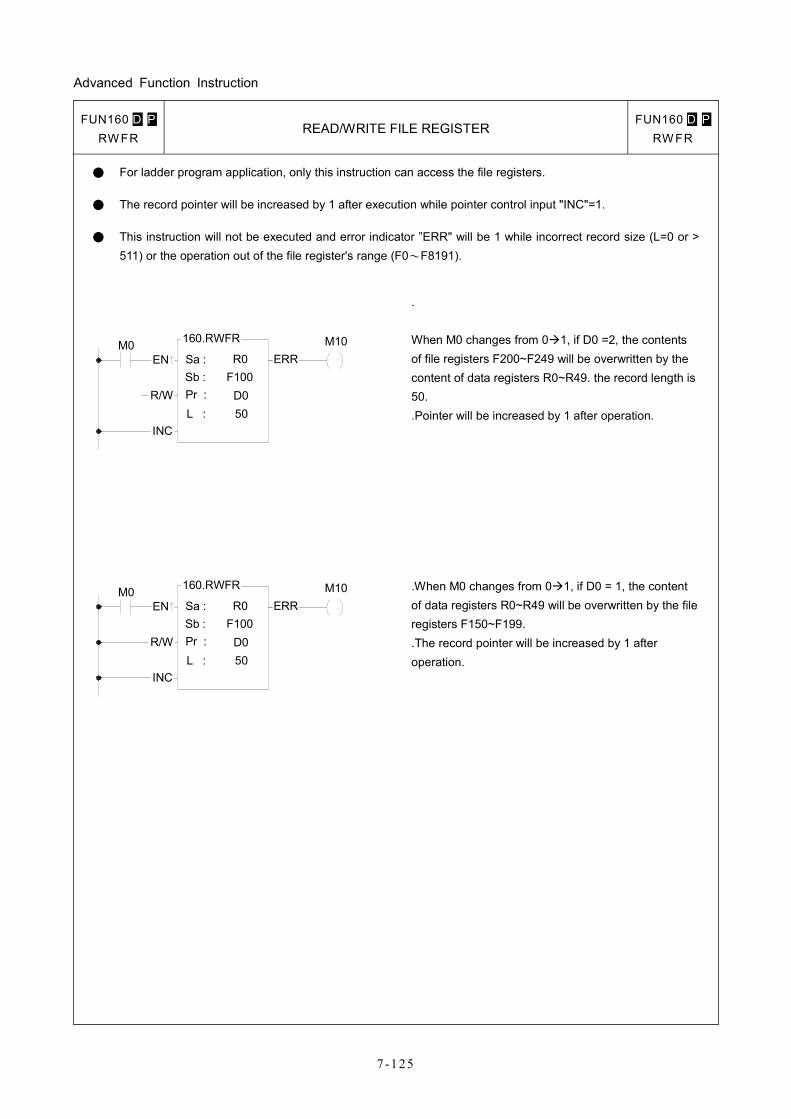
Advanced Function Instruction
7 -125
FUN160 D P RW FR
READ/WRITE FILE REGISTER FUN160 D P
RW FR
● For ladder program application, only this instruction can access the file registers.
● The record pointer will be increased by 1 after execution while pointer control input "INC"=1.
● This instruction will not be executed and error indicator ”ERR" will be 1 while incorrect record size (L=0 or > 511) or the operation out of the file register's range (F0~F8191).
M0EN Sa : R0
160.RWFR
Sb : F100
L :Pr :R/W
INC
ERR
50D0
M10
M0EN Sa : R0
160.RWFR
Sb : F100
L :Pr :R/W
INC
ERR
50D0
M10
. When M0 changes from 0 1, if D0 =2, the contents of file registers F200~F249 will be overwritten by the content of data registers R0~R49. the record length is 50. .Pointer will be increased by 1 after operation. .When M0 changes from 0 1, if D0 = 1, the content of data registers R0~R49 will be overwritten by the file registers F150~F199. .The record pointer will be increased by 1 after operation.
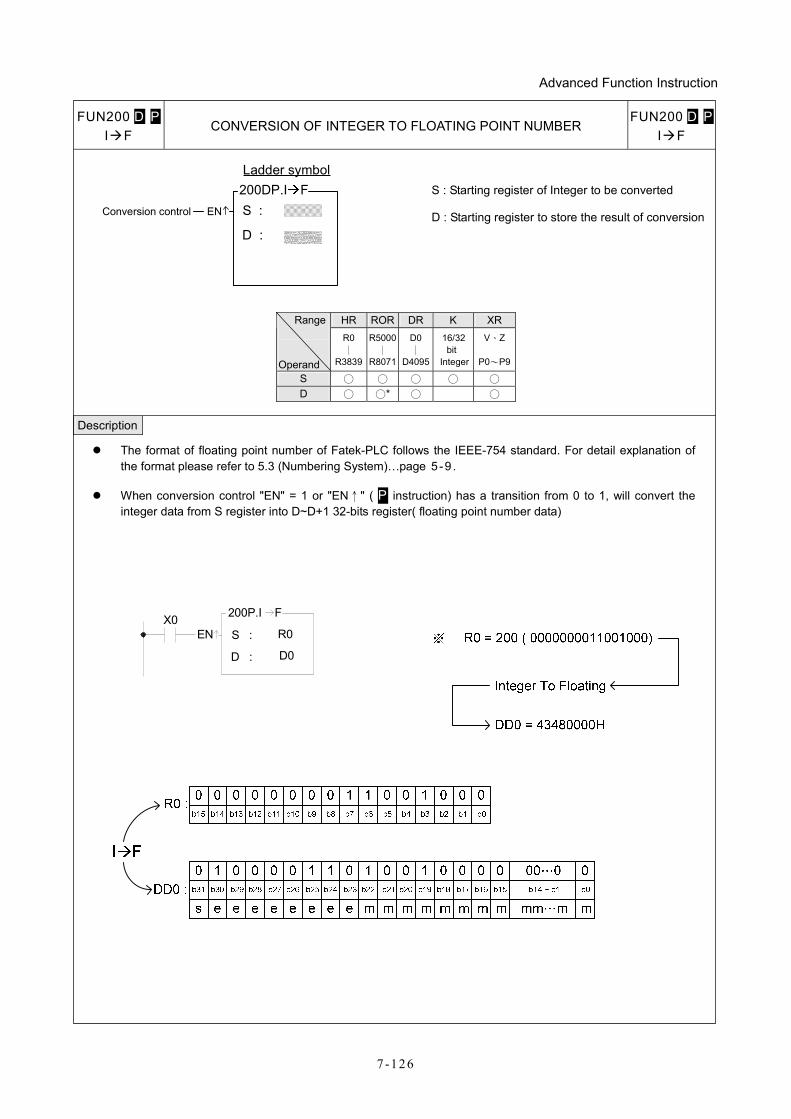
Advanced Function Instruction
7 -126
FUN200 D P I F
CONVERSION OF INTEGER TO FLOATING POINT NUMBER FUN200 D P
I F
S :ENConversion control
Ladder symbol 200DP.I F
D :
S : Starting register of Integer to be converted
D : Starting register to store the result of conversion
HR ROR DR K XR Range
Operand
R0 ∣
R3839
R5000∣
R8071
D0 ∣
D4095
16/32 bit Integer
V、Z
P0~P9
S ○ ○ ○ ○ ○ D ○ ○* ○ ○
Description
The format of floating point number of Fatek-PLC follows the IEEE-754 standard. For detail explanation of the format please refer to 5.3 (Numbering System)…page 5-9 .
When conversion control "EN" = 1 or "EN↑" ( P instruction) has a transition from 0 to 1, will convert the integer data from S register into D~D+1 32-bits register( floating point number data)
X0R0EN
200P.I F
D :
S :
D0
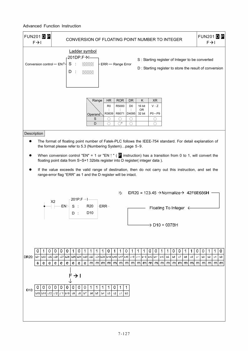
Advanced Function Instruction
7 -127
FUN201 D P F I
CONVERSION OF FLOATING POINT NUMBER TO INTEGER FUN201 D P
F I
S :ENConversion control
Ladder symbol 201DP.F I
D :
ERR Range Error
S : Starting register of Integer to be converted
D : Starting register to store the result of conversion
HR ROR DR K XR Range
Operand
R0 ∣
R3839
R5000∣
R8071
D0∣
D4095
16 bit OR 32 bit
V、Z
P0~P9
S ○ ○ ○ ○ D ○ ○* ○ ○
Description
The format of floating point number of Fatek-PLC follows the IEEE-754 standard. For detail explanation of the format please refer to 5.3 (Numbering System)…page 5-9 .
When conversion control "EN" = 1 or "EN↑" ( P instruction) has a transition from 0 to 1, will convert the floating point data from S~S+1 32bits register into D register( integer data ).
If the value exceeds the valid range of destination, then do not carry out this instruction, and set the range-error flag “ERR” as 1 and the D register will be intact.
X2EN
201P.F I
R20S :
D10D :
ERR
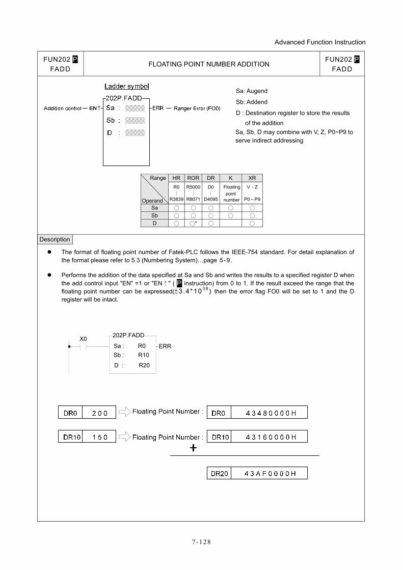
Advanced Function Instruction
7 -128
FUN202 P FADD
FLOATING POINT NUMBER ADDITION FUN202 P
FADD
Sa: Augend
Sb: Addend
D : Destination register to store the results of the addition
Sa, Sb, D may combine with V, Z, P0~P9 to serve indirect addressing
HR ROR DR K XR Range
Operand
R0∣
R3839
R5000∣
R8071
D0 ∣
D4095
Floatingpoint
number
V、Z
P0~P9
Sa ○ ○ ○ ○ ○ Sb ○ ○ ○ ○ ○ D ○ ○* ○ ○
Description
The format of floating point number of Fatek-PLC follows the IEEE-754 standard. For detail explanation of the format please refer to 5.3 (Numbering System)…page 5-9 .
Performs the addition of the data specified at Sa and Sb and writes the results to a specified register D when the add control input "EN" =1 or "EN↑" ( P instruction) from 0 to 1. If the result exceed the range that the floating point number can be expressed(±3.4*10 3 8) then the error flag FO0 will be set to 1 and the D register will be intact.
X0Sa : R0
202P.FADD
Sb : R10
D : R20
ERR
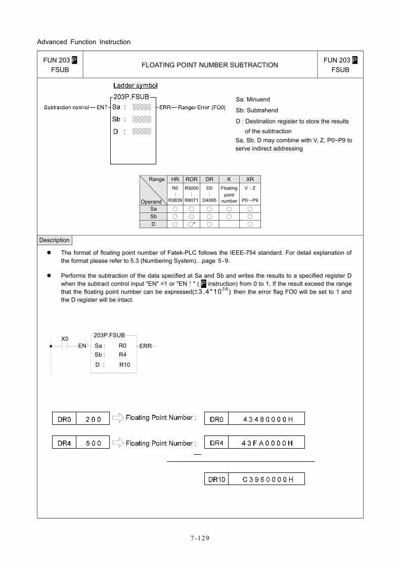
Advanced Function Instruction
7 -129
FUN 203 P FSUB
FLOATING POINT NUMBER SUBTRACTION FUN 203 P
FSUB
Sa: Minuend
Sb: Subtrahend
D : Destination register to store the results of the subtraction
Sa, Sb, D may combine with V, Z, P0~P9 to serve indirect addressing
HR ROR DR K XR Range
Operand
R0∣
R3839
R5000∣
R8071
D0 ∣
D4095
Floatingpoint
number
V、Z
P0~P9
Sa ○ ○ ○ ○ ○ Sb ○ ○ ○ ○ ○ D ○ ○* ○ ○
Description
The format of floating point number of Fatek-PLC follows the IEEE-754 standard. For detail explanation of the format please refer to 5.3 (Numbering System)…page 5-9 .
Performs the subtraction of the data specified at Sa and Sb and writes the results to a specified register D when the subtract control input "EN" =1 or "EN↑" ( P instruction) from 0 to 1. If the result exceed the range that the floating point number can be expressed(±3.4*103 8) then the error flag FO0 will be set to 1 and the D register will be intact.
X0Sa : R0
203P.FSUB
Sb : R4
D : R10
EN ERR
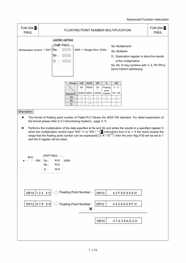
Advanced Function Instruction
7 -130
FUN 204 P FMUL
FLOATING POINT NUMBER MULTIPLICATION FUN 204 P
FMUL
Sa: Multiplicand
Sb: Multiplier
D : Destination register to store the results of the multiplication
Sa, Sb, D may combine with V, Z, P0~P9 to serve indirect addressing
HR ROR DR K XR Range
Operand
R0∣
R3839
R5000∣
R8071
D0 ∣
D4095
Floatingpoint
number
V、Z
P0~P9
Sa ○ ○ ○ ○ ○ Sb ○ ○ ○ ○ ○ D ○ ○* ○ ○
Description
The format of floating point number of Fatek-PLC follows the IEEE-754 standard. For detail explanation of the format please refer to 5.3 (Numbering System)…page 5-9 .
Performs the multiplication of the data specified at Sa and Sb and writes the results to a specified register D when the multiplication control input "EN" =1 or "EN↑" ( P instruction) from 0 to 1. If the result exceed the range that the floating point number can be expressed(±3.4*103 8) then the error flag FO0 will be set to 1 and the D register will be intact.
M10Sa : R10
204P.FMUL
Sb : R12
D : R14
EN ERR
DR10 1 2 3 . 4 5 Floating Point Number :
Floating Point Number :
DR10 4 2 F 6 E 6 6 6 H
4 4 2 9 A 2 8 F H
DR14 4 7 A 3 9 A E 2 H
DR12 6 7 8 . 5 4 DR12
×
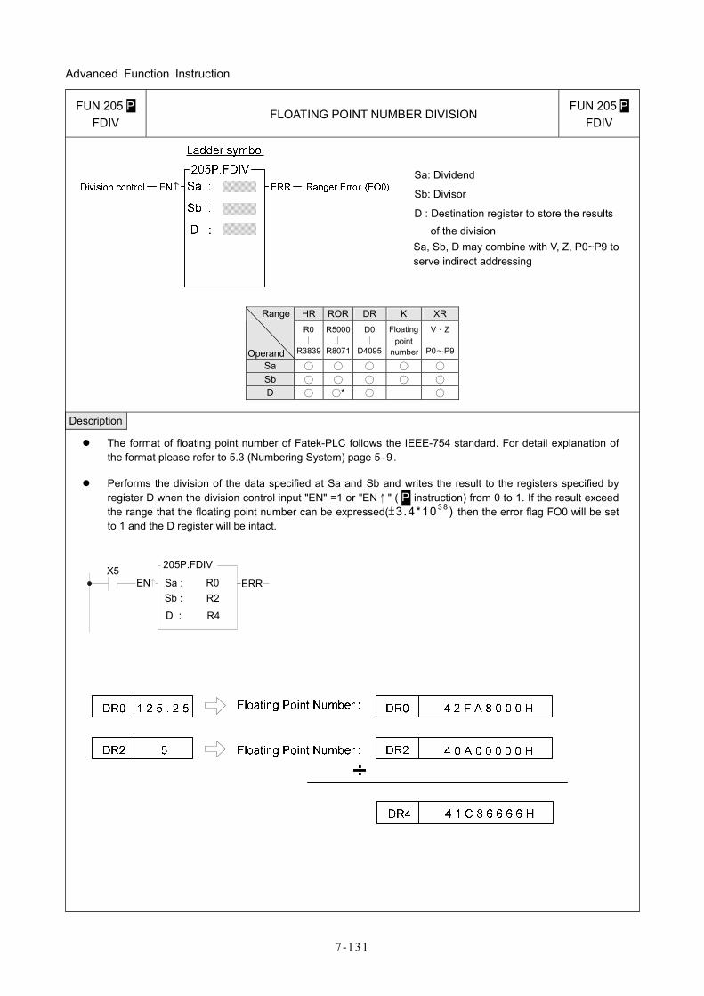
Advanced Function Instruction
7 -131
FUN 205 P FDIV
FLOATING POINT NUMBER DIVISION FUN 205 P
FDIV
Sa: Dividend
Sb: Divisor
D : Destination register to store the results of the division
Sa, Sb, D may combine with V, Z, P0~P9 to serve indirect addressing
HR ROR DR K XR Range
Operand
R0∣
R3839
R5000∣
R8071
D0 ∣
D4095
Floatingpoint
number
V、Z
P0~P9
Sa ○ ○ ○ ○ ○ Sb ○ ○ ○ ○ ○ D ○ ○* ○ ○
Description
The format of floating point number of Fatek-PLC follows the IEEE-754 standard. For detail explanation of the format please refer to 5.3 (Numbering System) page 5 -9.
Performs the division of the data specified at Sa and Sb and writes the result to the registers specified by register D when the division control input "EN" =1 or "EN↑" ( P instruction) from 0 to 1. If the result exceed the range that the floating point number can be expressed(±3.4*10 3 8) then the error flag FO0 will be set to 1 and the D register will be intact.
X5Sa : R0
205P.FDIV
Sb : R2
D : R4
EN ERR
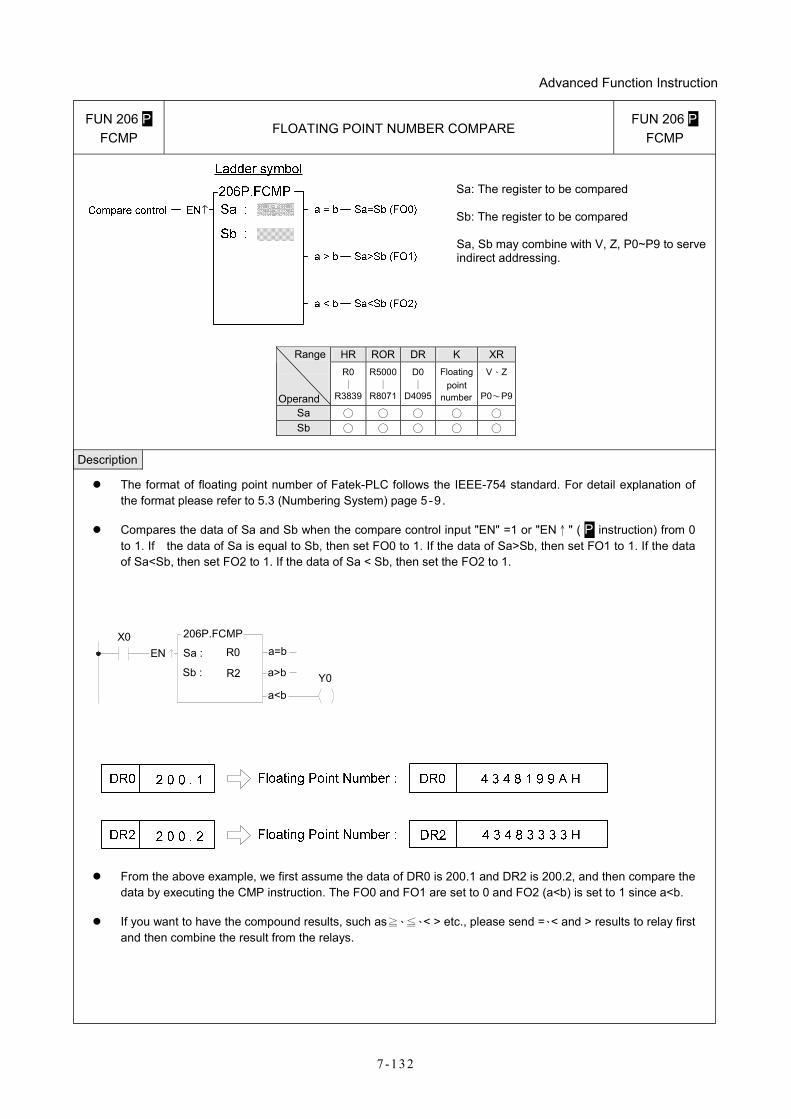
Advanced Function Instruction
7 -132
FUN 206 P FCMP
FLOATING POINT NUMBER COMPARE FUN 206 P
FCMP
Sa: The register to be compared Sb: The register to be compared Sa, Sb may combine with V, Z, P0~P9 to serve indirect addressing.
HR ROR DR K XR Range
Operand
R0 ∣
R3839
R5000∣
R8071
D0 ∣
D4095
Floatingpoint
number
V、Z
P0~P9
Sa ○ ○ ○ ○ ○ Sb ○ ○ ○ ○ ○
Description
The format of floating point number of Fatek-PLC follows the IEEE-754 standard. For detail explanation of the format please refer to 5.3 (Numbering System) page 5 -9.
Compares the data of Sa and Sb when the compare control input "EN" =1 or "EN↑" ( P instruction) from 0 to 1. If the data of Sa is equal to Sb, then set FO0 to 1. If the data of Sa>Sb, then set FO1 to 1. If the data of Sa<Sb, then set FO2 to 1. If the data of Sa < Sb, then set the FO2 to 1.
X0EN Sa :
Sb :
R0
R2
206P.FCMPa=b
a>b
a<bY0
From the above example, we first assume the data of DR0 is 200.1 and DR2 is 200.2, and then compare the data by executing the CMP instruction. The FO0 and FO1 are set to 0 and FO2 (a<b) is set to 1 since a<b.
If you want to have the compound results, such as≧、≦、< > etc., please send =、< and > results to relay first and then combine the result from the relays.
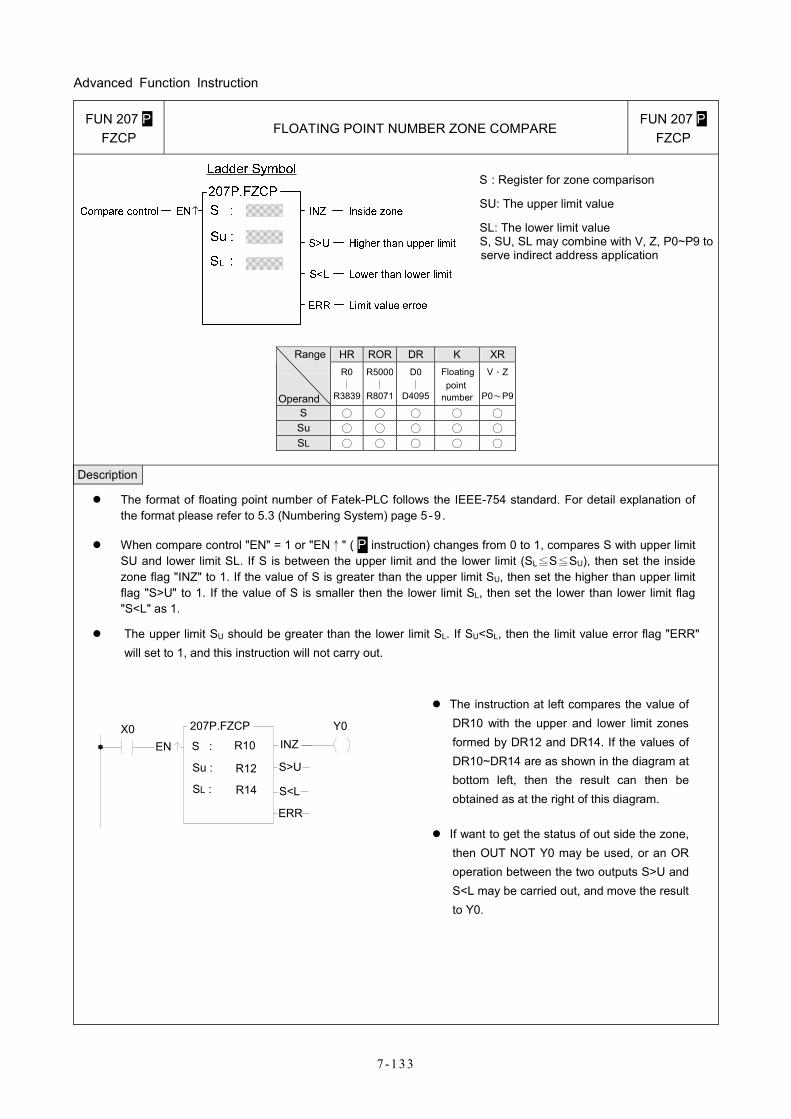
Advanced Function Instruction
7 -133
FUN 207 P FZCP
FLOATING POINT NUMBER ZONE COMPARE FUN 207 P
FZCP
S : Register for zone comparison
SU: The upper limit value
SL: The lower limit value S, SU, SL may combine with V, Z, P0~P9 to serve indirect address application
HR ROR DR K XR Range
Operand
R0∣
R3839
R5000∣
R8071
D0 ∣
D4095
Floating point number
V、Z
P0~P9
S ○ ○ ○ ○ ○ Su ○ ○ ○ ○ ○ SL ○ ○ ○ ○ ○
Description
The format of floating point number of Fatek-PLC follows the IEEE-754 standard. For detail explanation of the format please refer to 5.3 (Numbering System) page 5 -9.
When compare control "EN" = 1 or "EN↑" ( P instruction) changes from 0 to 1, compares S with upper limit SU and lower limit SL. If S is between the upper limit and the lower limit (SL≦S≦SU), then set the inside zone flag "INZ" to 1. If the value of S is greater than the upper limit SU, then set the higher than upper limit flag "S>U" to 1. If the value of S is smaller then the lower limit SL, then set the lower than lower limit flag "S<L" as 1.
The upper limit SU should be greater than the lower limit SL. If SU<SL, then the limit value error flag "ERR" will set to 1, and this instruction will not carry out.
X0EN S :
Su :
R10
R12
207P.FZCPINZ
S>U
Y0
SL : R14
ERR
S<L
The instruction at left compares the value of DR10 with the upper and lower limit zones formed by DR12 and DR14. If the values of DR10~DR14 are as shown in the diagram at bottom left, then the result can then be obtained as at the right of this diagram.
If want to get the status of out side the zone, then OUT NOT Y0 may be used, or an OR operation between the two outputs S>U and S<L may be carried out, and move the result to Y0.
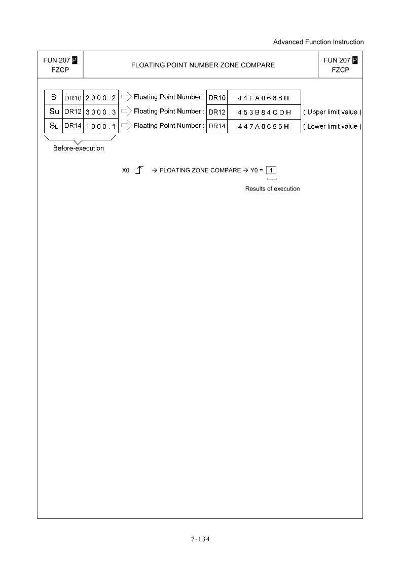
Advanced Function Instruction
7 -134
FUN 207 P FZCP
FLOATING POINT NUMBER ZONE COMPARE FUN 207 P
FZCP
X0= FLOATING ZONE COMPARE Y0 = 1
Results of execution
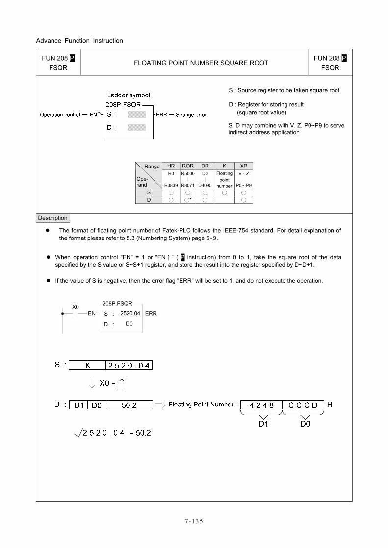
Advance Function Instruction
7 -135
FUN 208 P FSQR
FLOATING POINT NUMBER SQUARE ROOT FUN 208 P
FSQR
S : Source register to be taken square root
D : Register for storing result (square root value)
S, D may combine with V, Z, P0~P9 to serve indirect address application
HR ROR DR K XR Range
Ope- rand
R0 ∣
R3839
R5000∣
R8071
D0 ∣
D4095
Floatingpoint
number
V、Z
P0~P9S ○ ○ ○ ○ ○ D ○ ○* ○ ○
Description
The format of floating point number of Fatek-PLC follows the IEEE-754 standard. For detail explanation of the format please refer to 5.3 (Numbering System) page 5 -9.
When operation control "EN" = 1 or "EN↑" ( P instruction) from 0 to 1, take the square root of the data specified by the S value or S~S+1 register, and store the result into the register specified by D~D+1.
If the value of S is negative, then the error flag "ERR" will be set to 1, and do not execute the operation.
X0EN
208P.FSQR
2520.04S :
D0D :
ERR
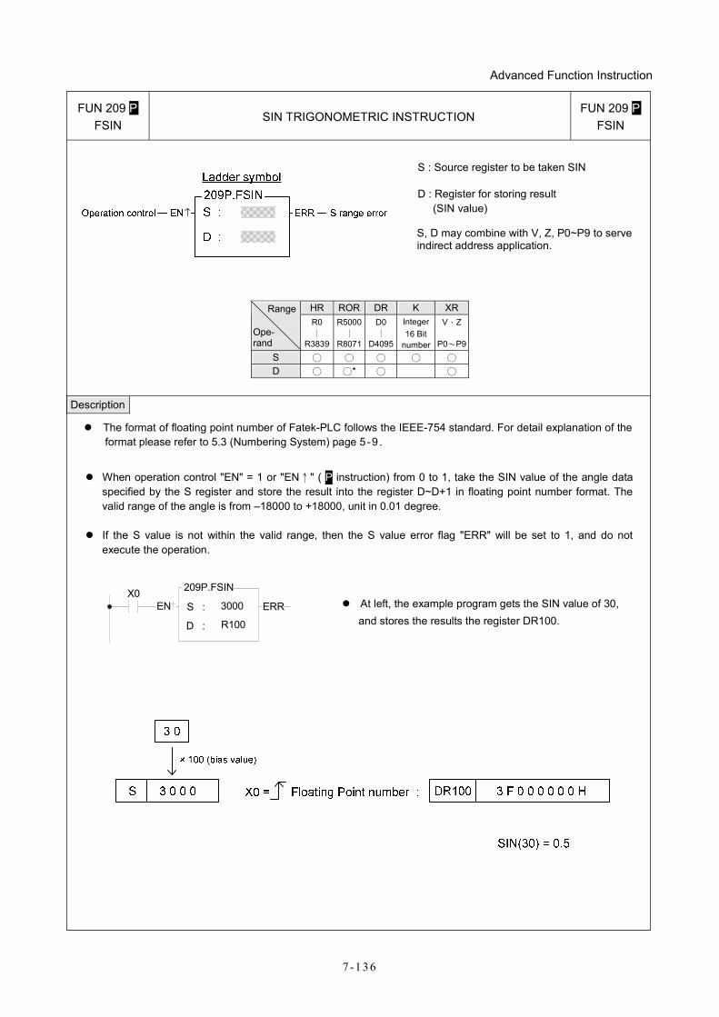
Advanced Function Instruction
7 -136
FUN 209 P FSIN
SIN TRIGONOMETRIC INSTRUCTION FUN 209 P
FSIN
S : Source register to be taken SIN
D : Register for storing result (SIN value)
S, D may combine with V, Z, P0~P9 to serve indirect address application.
HR ROR DR K XR Range
Ope- rand
R0 ∣
R3839
R5000∣
R8071
D0 ∣
D4095
Integer16 Bit
number
V、Z
P0~P9S ○ ○ ○ ○ ○ D ○ ○* ○ ○
Description
The format of floating point number of Fatek-PLC follows the IEEE-754 standard. For detail explanation of the format please refer to 5.3 (Numbering System) page 5 -9 .
When operation control "EN" = 1 or "EN↑" ( P instruction) from 0 to 1, take the SIN value of the angle data specified by the S register and store the result into the register D~D+1 in floating point number format. The valid range of the angle is from –18000 to +18000, unit in 0.01 degree.
If the S value is not within the valid range, then the S value error flag "ERR" will be set to 1, and do not execute the operation.
X0EN
209P.FSIN
3000S :
R100D :
ERR
At left, the example program gets the SIN value of 30, and stores the results the register DR100.
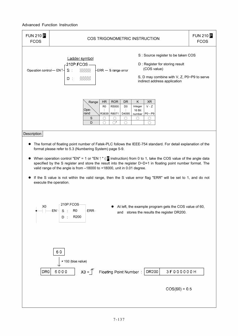
Advanced Function Instruction
7 -137
FUN 210 P FCOS
COS TRIGONOMETRIC INSTRUCTION FUN 210 P
FCOS
S : Source register to be taken COS
D : Register for storing result (COS value)
S, D may combine with V, Z, P0~P9 to serve indirect address application
HR ROR DR K XR Range
Ope- rand
R0∣
R3839
R5000∣
R8071
D0 ∣
D4095
Integer16 Bit
number
V、Z
P0~P9S ○ ○ ○ ○ ○ D ○ ○* ○ ○
Description
The format of floating point number of Fatek-PLC follows the IEEE-754 standard. For detail explanation of the format please refer to 5.3 (Numbering System) page 5-9.
When operation control "EN" = 1 or "EN↑" ( P instruction) from 0 to 1, take the COS value of the angle data specified by the S register and store the result into the register D~D+1 in floating point number format. The valid range of the angle is from –18000 to +18000, unit in 0.01 degree.
If the S value is not within the valid range, then the S value error flag "ERR" will be set to 1, and do not execute the operation.
X0EN
210P.FCOS
R0S :
R200D :
ERR
At left, the example program gets the COS value of 60, and stores the results the register DR200.
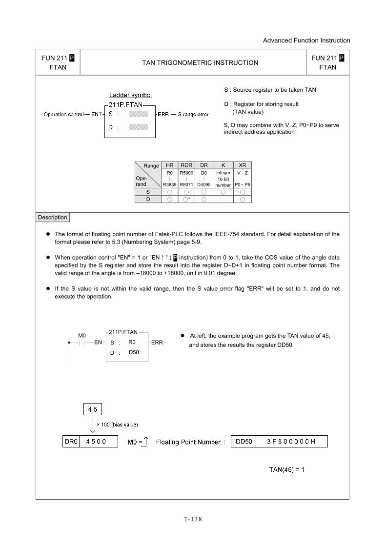
Advanced Function Instruction
7 -138
FUN 211 P FTAN
TAN TRIGONOMETRIC INSTRUCTION FUN 211 P
FTAN
S : Source register to be taken TAN
D : Register for storing result (TAN value)
S, D may combine with V, Z, P0~P9 to serve indirect address application
HR ROR DR K XR Range
Ope- rand
R0 ∣
R3839
R5000∣
R8071
D0 ∣
D4095
Integer16 Bit
number
V、Z
P0~P9S ○ ○ ○ ○ ○ D ○ ○* ○ ○
Description
The format of floating point number of Fatek-PLC follows the IEEE-754 standard. For detail explanation of the format please refer to 5.3 (Numbering System) page 5-9.
When operation control "EN" = 1 or "EN↑" ( P instruction) from 0 to 1, take the COS value of the angle data specified by the S register and store the result into the register D~D+1 in floating point number format. The valid range of the angle is from –18000 to +18000, unit in 0.01 degree.
If the S value is not within the valid range, then the S value error flag "ERR" will be set to 1, and do not execute the operation.
M0EN
211P.FTAN
R0S :
D50D :
ERR
At left, the example program gets the TAN value of 45, and stores the results the register DD50.
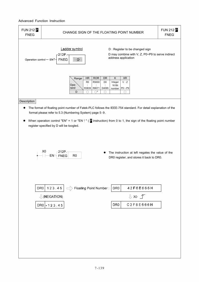
Advanced Function Instruction
7 -139
FUN 212 P FNEG
CHANGE SIGN OF THE FLOATING POINT NUMBER FUN 212 P
FNEG
D : Register to be changed sign
D may combine with V, Z, P0~P9 to serve indirect address application
HR ROR DR K XR Range
Ope- rand
R0 ∣
R3839
R5000∣
R8071
D0 ∣
D4095
Integer16 Bit
number
V、Z
P0~P9D ○ ○* ○ ○
Description
The format of floating point number of Fatek-PLC follows the IEEE-754 standard. For detail explanation of the format please refer to 5.3 (Numbering System) page 5 -9 .
When operation control "EN" = 1 or "EN↑" ( P instruction) from 0 to 1, the sign of the floating point number register specified by D will be toogled.
ENX0 212P.
FNEG R0
The instruction at left negates the value of the DR0 register, and stores it back to DR0.
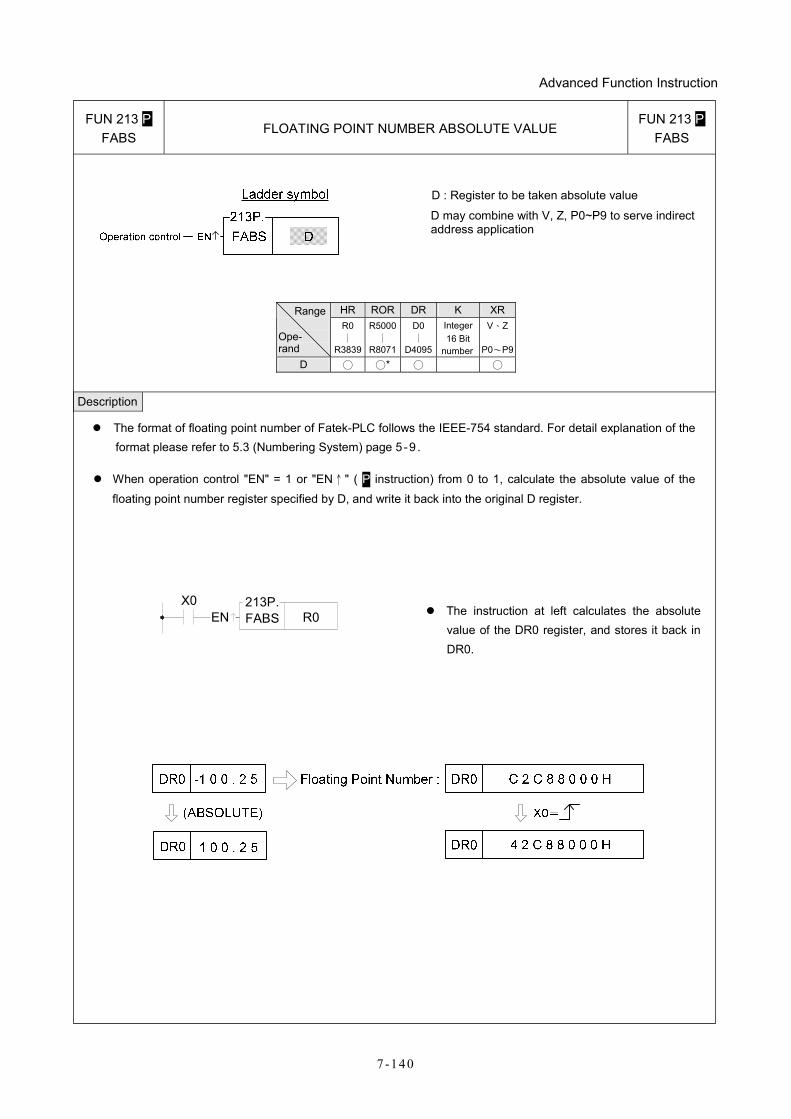
Advanced Function Instruction
7 -140
FUN 213 P FABS
FLOATING POINT NUMBER ABSOLUTE VALUE FUN 213 P
FABS
D : Register to be taken absolute value
D may combine with V, Z, P0~P9 to serve indirect address application
HR ROR DR K XR Range
Ope- rand
R0 ∣
R3839
R5000∣
R8071
D0 ∣
D4095
Integer16 Bit
number
V、Z
P0~P9D ○ ○* ○ ○
Description
The format of floating point number of Fatek-PLC follows the IEEE-754 standard. For detail explanation of the format please refer to 5.3 (Numbering System) page 5 -9 .
When operation control "EN" = 1 or "EN↑" ( P instruction) from 0 to 1, calculate the absolute value of the floating point number register specified by D, and write it back into the original D register.
R0X0
EN213P.FABS
The instruction at left calculates the absolute value of the DR0 register, and stores it back in DR0.

MEMO
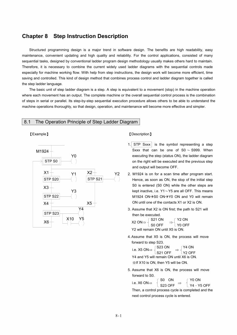
8-1
Chapter 8 Step Instruction Description
Structured programming design is a major trend in software design. The benefits are high readability, easy maintenance, convenient updating and high quality and reliability. For the control applications, consisted of many sequential tasks, designed by conventional ladder program design methodology usually makes others hard to maintain. Therefore, it is necessary to combine the current widely used ladder diagrams with the sequential controls made especially for machine working flow. With help from step instructions, the design work will become more efficient, time saving and controlled. This kind of design method that combines process control and ladder diagram together is called the step ladder language.
The basic unit of step ladder diagram is a step. A step is equivalent to a movement (stop) in the machine operation where each movement has an output. The complete machine or the overall sequential control process is the combination of steps in serial or parallel. Its step-by-step sequential execution procedure allows others to be able to understand the machine operations thoroughly, so that design, operation, and maintenance will become more effective and simpler.
8.1 The Operation Principle of Step Ladder Diagram
【Example】 【Description】
Y1
Y3
Y0
Y4
Y5
M1924
X1
X3
X4
X2 Y2
X5
X6X10
STP S20
STP S22
STP S23
STP S21
STP S0
1. STP Sxxx is the symbol representing a step Sxxx that can be one of S0 ~ S999. When executing the step (status ON), the ladder diagram on the right will be executed and the previous step and output will become OFF.
2. M1924 is on for a scan time after program start. Hence, as soon as ON, the stop of the initial step S0 is entered (S0 ON) while the other steps are kept inactive, i.e. Y1~Y5 are all OFF. This means M1924 ON S0 ON Y0 ON and Y0 will remain ON until one of the contacts X1 or X2 is ON.
3. Assume that X2 is ON first; the path to S21 will then be executed.
X2 ON⇒ ⇒
Y2 will remain ON until X5 is ON.
4. Assume that X5 is ON, the process will move forward to step S23.
i.e. X5 ON⇒ ⇒
Y4 and Y5 will remain ON until X6 is ON. ※If X10 is ON, then Y5 will be ON.
5. Assume that X6 is ON, the process will move forward to S0.
i.e. X6 ON⇒ ⇒
Then, a control process cycle is completed and the next control process cycle is entered.
S23 ON S21 OFF
Y4 ON Y2 OFF
S21 ON S0 OFF
Y2 ON Y0 OFF
S0 ON S23 OFF
Y0 ON Y4、Y5 OFF
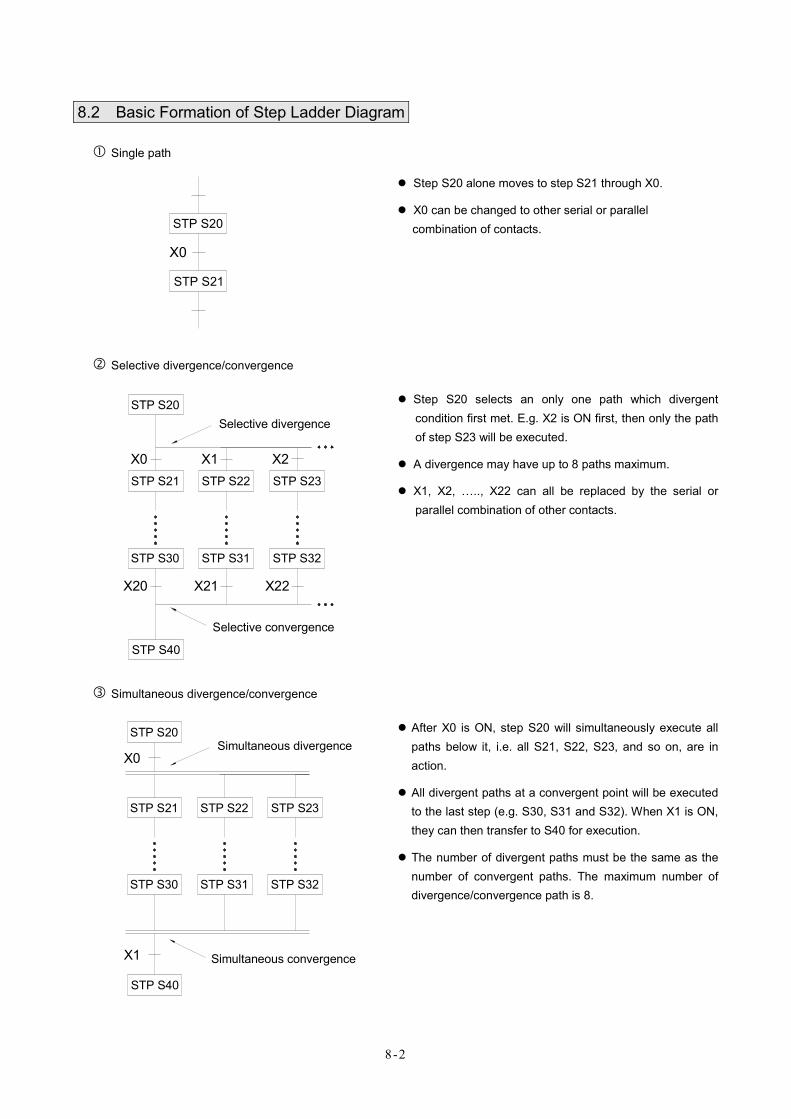
8-2
8.2 Basic Formation of Step Ladder Diagram
Single path
STP S20
STP S21
X0
Step S20 alone moves to step S21 through X0.
X0 can be changed to other serial or parallel combination of contacts.
Selective divergence/convergence
STP S40
X21
STP S31
X22
STP S32
STP S22
X1STP S23
X2
Selective divergence
Selective convergence
X0
X20
STP S21
STP S30
STP S20
Step S20 selects an only one path which divergent condition first met. E.g. X2 is ON first, then only the path of step S23 will be executed.
A divergence may have up to 8 paths maximum.
X1, X2, ….., X22 can all be replaced by the serial or parallel combination of other contacts.
Simultaneous divergence/convergence
STP S21
STP S30
STP S40
STP S20
STP S22
STP S31
STP S23
STP S32
X1
X0Simultaneous divergence
Simultaneous convergence
After X0 is ON, step S20 will simultaneously execute all paths below it, i.e. all S21, S22, S23, and so on, are in action.
All divergent paths at a convergent point will be executed to the last step (e.g. S30, S31 and S32). When X1 is ON, they can then transfer to S40 for execution.
The number of divergent paths must be the same as the number of convergent paths. The maximum number of divergence/convergence path is 8.
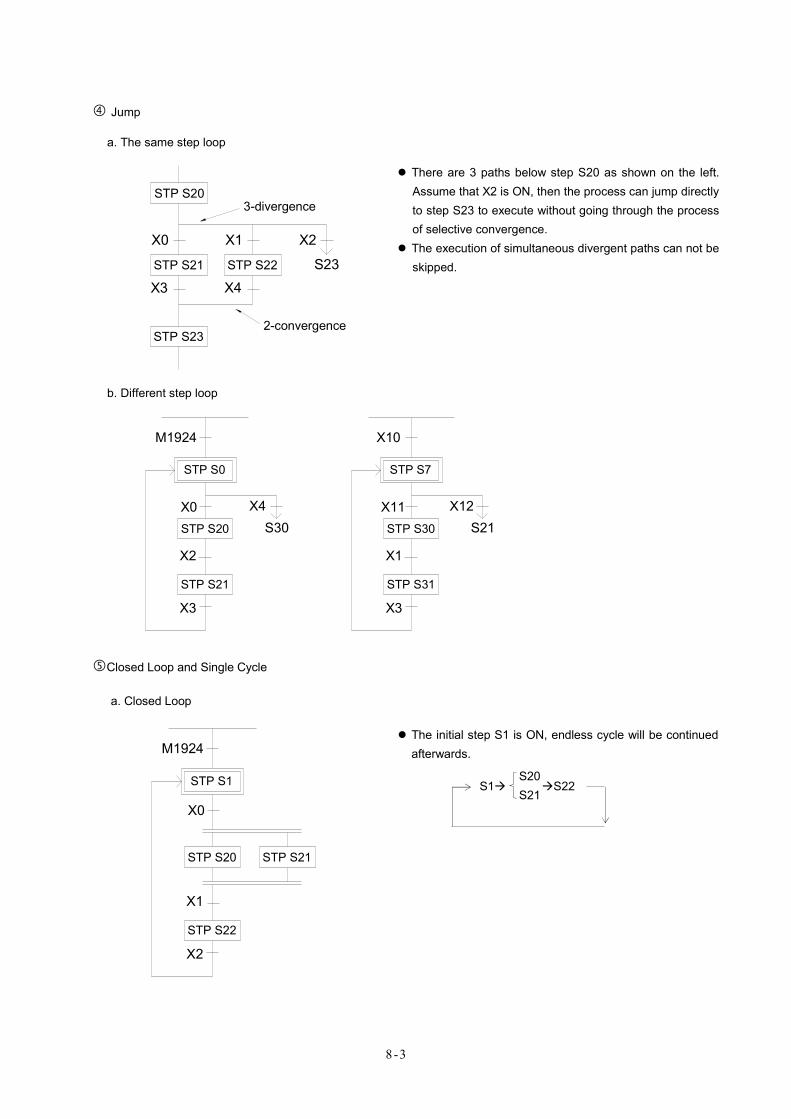
8-3
Jump
a. The same step loop
STP S20
X0
X3STP S21
STP S23
X1
X4STP S22
X2
S23
3-divergence
2-convergence
There are 3 paths below step S20 as shown on the left. Assume that X2 is ON, then the process can jump directly to step S23 to execute without going through the process of selective convergence.
The execution of simultaneous divergent paths can not be skipped.
b. Different step loop
M1924
X0
X2
X3
STP S20
STP S21
X4S30
X10
STP S7
X11
X1
X3
STP S30
STP S31
X12S21
STP S0
Closed Loop and Single Cycle
a. Closed Loop
M1924
STP S1
STP S20
STP S22
X0
X1
X2
STP S21
The initial step S1 is ON, endless cycle will be continued afterwards.
S1 S22
S20 S21
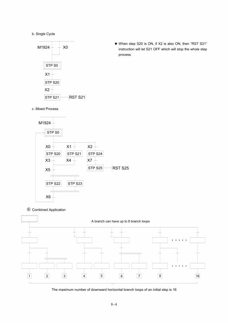
8-4
b. Single Cycle
M1924
STP S0
STP S20
X1
X2
STP S21
X0
RST S21
When step S20 is ON, if X2 is also ON, then “RST S21” instruction will let S21 OFF which will stop the whole step process.
c. Mixed Process
M1924
STP S0
X4X3
X2X0 X1
STP S20 STP S21 STP S24
X7
X5
STP S22 STP S23
X6
STP S25 RST S25
Combined Application
A branch can have up to 8 branch loops
1 2 3 4 5 6 7 8 16
The maximum number of downward horizontal branch loops of an initial step is 16
8-5
8.3 Introduction of Step Instructions: STP, FROM, TO and STPEND
● STP Sx : S0≦Sx≦S7 (Displayed in WinProladder)
or STP Sx :S0≦Sx≦S7 (Displayed in FP-07)
This instruction is the initial step instruction from where the step control of each machine process can be derived. Up to 8 initial steps can be used in the FBs series, i.e. a PLC can make up to 8 process controls simultaneously. Each step process can operate independently or generate results for the reference of other processes.
【Example 1】 Go to the initial step S0 after each start (ON)
WinProladder FP-07
M1924
STP S0
M1924
STP S0
TO S0
ORG TO STP
M1924 S0 S0
【Example 2】 Each time the device is start to run or the manual button is pressed or the device is malfunction, then the device automatically enters the initial step S0 to standby.
WinProladder FP-07
ORG OR OR TO STP
M1924 X0 M0 S0 S0
M1924 X0 M0
STP S0
M1924
STP S0
X0
M0
StandbyProcessProgram
TO S0
Standby process program
【Description】X0: Manual Button, M0: Abnormal Contact.
8-6
● STP Sxxx : S20≦Sxxx≦S999(Displayed in WinProladder)
or STP Sxxx : S20≦Sxxx≦S999(Displayed in FP-07)
This instruction is a step instruction, each step in a process represents a step of sequence. If the status of step is ON then the step is active and will execute the ladder program associate to the step.
【Example】
WinProladder FP-07
Y1
Y0
Y2
M1924
STP S0
X11X2
STP S20X1
X10
M1924
STP S0
Y1
Y0
Y2
STPEND
X10
X11
X2STP S20
X1
TO S0
TO S0
TO S20
ORG TO STP OUT FROM AND TO STP OUT AND OUT LD AND OUT FROM AND TO STPEND
M1924 S0 S0 Y0 S0 X10 S20 S20 TR0 X1 Y1 TR0 X2 Y2 S20 X11 S0
【Description】1. When ON, the initial step S0 is ON and Y0 is ON.
2. When transfer condition X10 is ON (in actual application, the transferring condition may be formed by the serial or parallel combination of the contacts X, Y, M, T and C), the step S20 is activated. The system will automatically turn S0 OFF in the current scan cycle and Y0 will be reset automatically to OFF.
i.e. X10 ON⇒
S20 ON S0 OFF
⇒ X1 ON X2 ON Y0 OFF
Y1 ON Y2 ON
3. When the transfer condition X11 is ON, the step S0 is ON, Y0 is ON and S20, Y1 and Y2 will turn OFF at the same time.
i.e. X11 ON⇒
S0 ON S20 OFF
⇒ Y0 ON Y1 OFF Y2 OFF
8-7
● FROM Sxxx : S0≦Sxxx≦S999(Displayed in WinProladder)
or FROM Sxxx : S0≦Sxxx≦S999(Displayed in FP-07)
The instruction describes the source step of the transfer, i.e. moving from step Sxxx to the next step in coordination with transfer condition.
【Example】
WinProladder FP-07
Y0
Y4
M1924
STP S0
X1
X5
X7
X8
STP S20
STP S23
X0
Y1
X4
S0
Y2X2
STP S21
X6
X3
STP S22Y3
M1924
STP S0
Y1
Y0
Y2
STPEND
X1
STP S20
X2
X3
X0
STP S21X4
Y3STP S22
X7X5
X6
Y4
X8
TO S20
TO S21
TO S22
TO S0
TO S0
TO S23
TO S0
FROM S22
FROM S20
STP S23
ORG TO STP AND OUT FROM OUT TR AND TO LD TR AND TO LD TR AND TO STP OUT STP OUT FROM AND TO STP OUT FROM AND FROM AND ORLD AND TO STP OUT FROM AND TO STPEND
M1924S0 S0 X0 Y0 S0 0 X1 S20 0 X2 S21 0 X3 S22 S20 Y1 S21 Y2 S21 X4 S0 S22 Y3 S20 X5 S22 X6 X7 S23 S23 Y4 S23 X8 S0
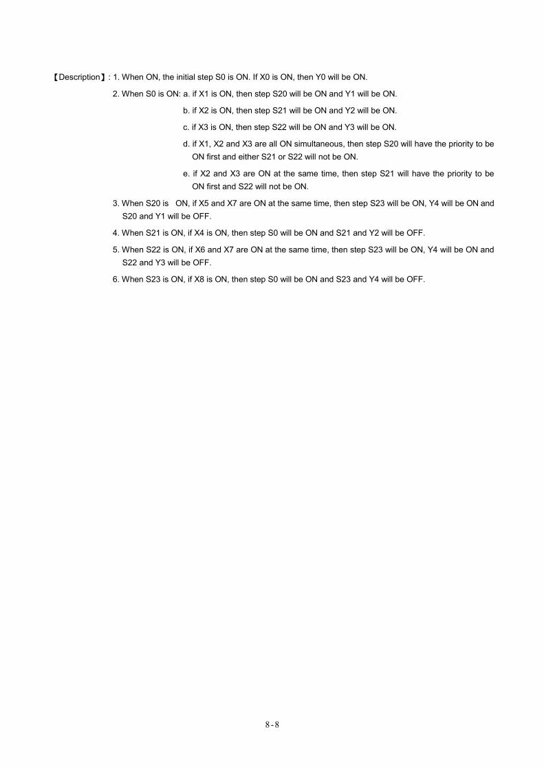
8-8
【Description】: 1. When ON, the initial step S0 is ON. If X0 is ON, then Y0 will be ON.
2. When S0 is ON: a. if X1 is ON, then step S20 will be ON and Y1 will be ON.
b. if X2 is ON, then step S21 will be ON and Y2 will be ON.
c. if X3 is ON, then step S22 will be ON and Y3 will be ON.
d. if X1, X2 and X3 are all ON simultaneous, then step S20 will have the priority to be ON first and either S21 or S22 will not be ON.
e. if X2 and X3 are ON at the same time, then step S21 will have the priority to be ON first and S22 will not be ON.
3. When S20 is ON, if X5 and X7 are ON at the same time, then step S23 will be ON, Y4 will be ON and S20 and Y1 will be OFF.
4. When S21 is ON, if X4 is ON, then step S0 will be ON and S21 and Y2 will be OFF.
5. When S22 is ON, if X6 and X7 are ON at the same time, then step S23 will be ON, Y4 will be ON and S22 and Y3 will be OFF.
6. When S23 is ON, if X8 is ON, then step S0 will be ON and S23 and Y4 will be OFF.
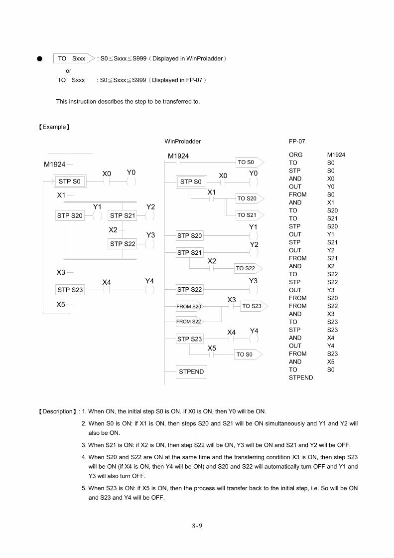
8-9
● TO Sxxx : S0≦Sxxx≦S999(Displayed in WinProladder)
or TO Sxxx : S0≦Sxxx≦S999(Displayed in FP-07)
This instruction describes the step to be transferred to.
【Example】
WinProladder FP-07
Y1
Y0M1924
STP S0
STP S20
X0
X1Y2
STP S21
Y3STP S22
STP S23
X2
X3
X5
Y4X4
M1924
STP S0
Y1
Y0
Y2
STPEND
X1
STP S20
X2
X4
X0
STP S21
Y3STP S22
X3
Y4
X5
TO S20
TO S21
TO S22
TO S0
TO S23
TO S0
FROM S22
FROM S20
STP S23
ORG TO STP AND OUT FROM AND TO TO STP OUT STP OUT FROM AND TO STP OUT FROM FROM AND TO STP AND OUT FROM AND TO STPEND
M1924 S0 S0 X0 Y0 S0 X1 S20 S21 S20 Y1 S21 Y2 S21 X2 S22 S22 Y3 S20 S22 X3 S23 S23 X4 Y4 S23 X5 S0
【Description】: 1. When ON, the initial step S0 is ON. If X0 is ON, then Y0 will be ON.
2. When S0 is ON: if X1 is ON, then steps S20 and S21 will be ON simultaneously and Y1 and Y2 will also be ON.
3. When S21 is ON: if X2 is ON, then step S22 will be ON, Y3 will be ON and S21 and Y2 will be OFF.
4. When S20 and S22 are ON at the same time and the transferring condition X3 is ON, then step S23 will be ON (if X4 is ON, then Y4 will be ON) and S20 and S22 will automatically turn OFF and Y1 and Y3 will also turn OFF.
5. When S23 is ON: if X5 is ON, then the process will transfer back to the initial step, i.e. So will be ON and S23 and Y4 will be OFF.
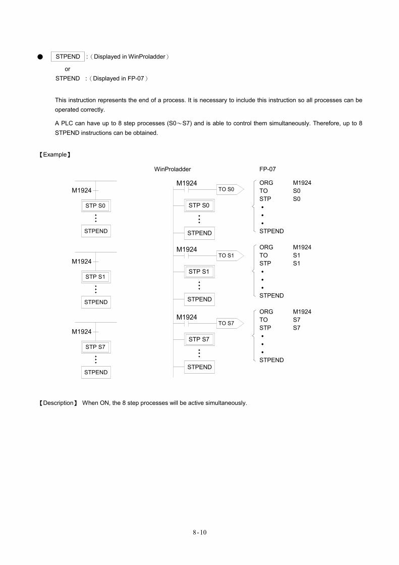
8-10
● STPEND :(Displayed in WinProladder)
or STPEND :(Displayed in FP-07)
This instruction represents the end of a process. It is necessary to include this instruction so all processes can be operated correctly.
A PLC can have up to 8 step processes (S0~S7) and is able to control them simultaneously. Therefore, up to 8 STPEND instructions can be obtained.
【Example】
WinProladder FP-07
M1924
STPEND
M1924
STPEND
STPEND
M1924
STP S1
STP S0
STP S7
M1924
STPEND
STP S0
TO S0
STPEND
M1924
M1924
STPEND
TO S1
STP S1
TO S7
STP S7
ORG TO STP ˙ ˙ ˙ STPEND ORG TO STP ˙ ˙ ˙ STPEND ORG TO STP ˙ ˙ ˙ STPEND
M1924 S0 S0 M1924 S1 S1 M1924 S7 S7
【Description】 When ON, the 8 step processes will be active simultaneously.
8-11
8.4 Notes for Writing a Step Ladder Diagram
【Notes】
● In actual applications, the ladder diagram can be used together with the step ladder.
● There are 8 steps, S0~S7, that can be used as the starting point and are called the “initial steps”.
● When PLC starts operating, it is necessary to activate the initial step. The M1924 (the first scan ON signal) provided by the system may be used to activate the initial step.
● Except the initial step, the start of any other steps must be driven by other step.
● It is necessary to have an initial step and the final STPEND instruction in a step ladder diagram to complete a step process program.
● There are 980 steps, S20~S999, available that can be used freely. However, used numbers cannot be repeated. S500~S999 are retentive(The range can be modified by users), can be used if it is required to continue the machine process after power is off.
● Basically a step must consists of three parts which are control output, transition conditions and transition targets.
● MC and SKP instructions cannot be used in a step program and the sub-programs. It’s recommended that JMP instruction should be avoided as much as possible.
● If the output point is required to stay ON after the step is divergent to other step, it is necessary to use the SET instruction to control the output point and use RST instruction to clear the output point to OFF.
● Looking down from an initial step, the maximum number of horizontal paths is 16. However, a step is only allowed to have up to 8 branch paths.
● When M1918=0(default), if a PULSE type function instruction is used in master control loop (FUN 0) or a step program, it is necessary to connect a TU instruction before the function instruction. For example,
C0
PV : 5
STP S20S20
When M1918=1, the TU instruction is not required, e.g.:
PV : 5
C0STP S20
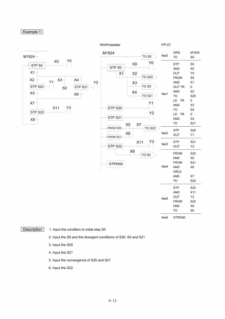
8-12
Example 1
WinProladder FP-07
Net0 ORG TO
M1924S0
Net1
STP AND OUT FROM AND OUT TR AND TO LD TR AND TO LD TR AND TO
S0 X0 Y0 S0 X1 0 X2 S20 0 X3 S0 0 X4 S21
Net2 STP OUT
S20 Y1
Net3 STP OUT
S21 Y2
Net4
FROM AND FROM AND ORLD AND TO
S20 X5 S21 X6 X7 S22
Net5
STP AND OUT FROM AND TO
S22 X11 Y3 S22 X8 S0
Y1
Y0M1924
STP S0
X5
X2
STP S20
X0
X3
S0
X1
X6
Y2X4
STP S21
X8
X7Y3X11
STP S22
M1924
STP S0
Y1
Y0
Y2
STPEND
STP S20
X2
X3
X0
STP S21
X4
X7X5
X6
Y3STP S22
X8
TO S20
TO S0
TO S21
TO S0
TO S22
TO S0
FROM S20
X1
X11FROM S21
Net6 STPEND
Description 1. Input the condition to initial step S0
2. Input the S0 and the divergent conditions of S20, S0 and S21
3. Input the S20
4. Input the S21
5. Input the convergence of S20 and S21
6. Input the S22
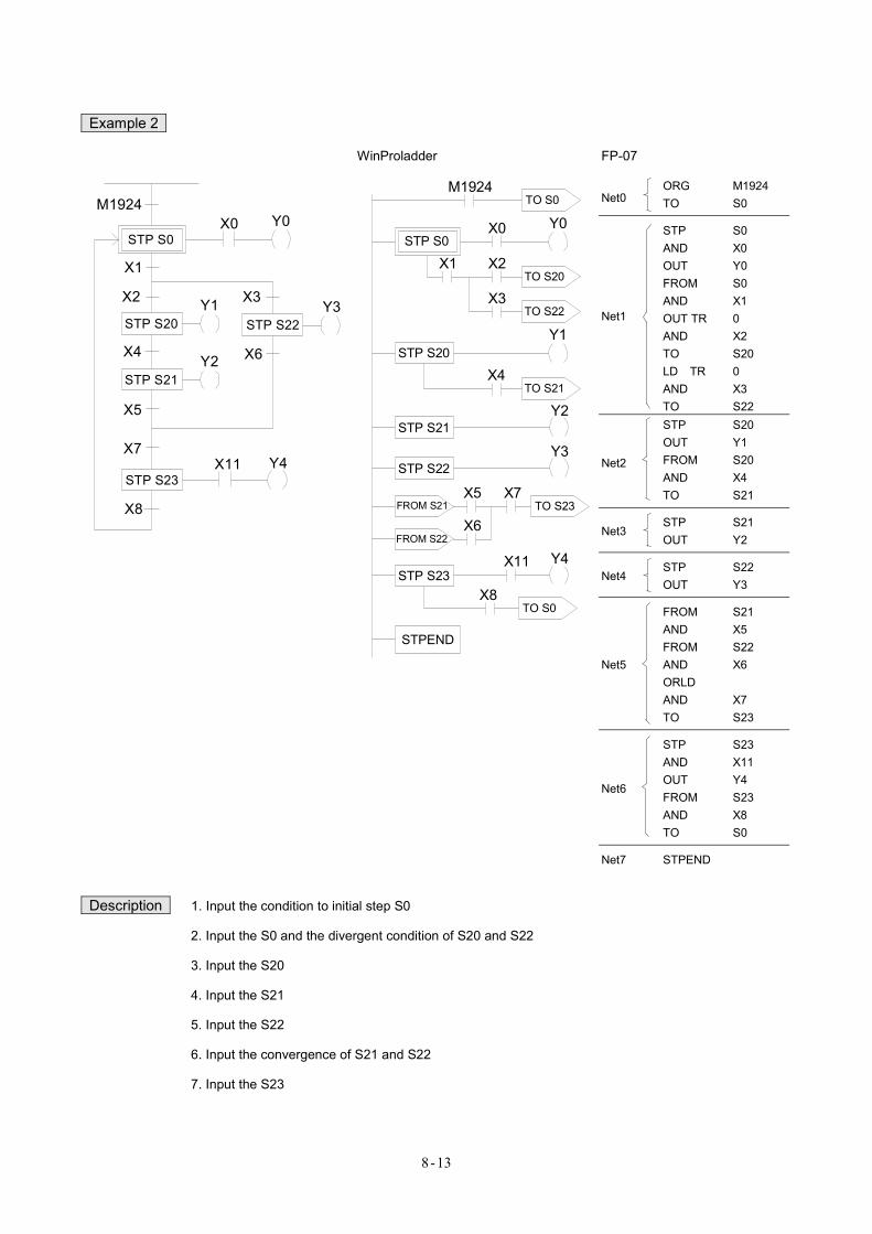
8-13
Example 2
WinProladder FP-07
Net0 ORG TO
M1924 S0
Net1
STP AND OUT FROM AND OUT TR AND TO LD TR AND TO
S0 X0 Y0 S0 X1 0 X2 S20 0 X3 S22
Net2
STP OUT FROM AND TO
S20 Y1 S20 X4 S21
Net3 STP OUT
S21 Y2
Net4 STP OUT
S22 Y3
Net5
FROM AND FROM AND ORLD AND TO
S21 X5 S22 X6 X7 S23
Net6
STP AND OUT FROM AND TO
S23 X11 Y4 S23 X8 S0
Y1
Y0M1924
STP S0
X2
STP S20
X0
X1
X4 X6
X7X11
STP S21
X5
STP S23
X8
Y2
STP S22
X3Y3
Y4
M1924
STP S0
Y1
Y0
Y2
STPEND
STP S20
X2
X3
X0
STP S21
X4
X7X5
X6
Y3STP S22
X8
TO S20
TO S22
TO S21
TO S0
TO S23
TO S0
FROM S22
FROM S21
X1
X11 Y4STP S23
Net7 STPEND
Description 1. Input the condition to initial step S0
2. Input the S0 and the divergent condition of S20 and S22
3. Input the S20
4. Input the S21
5. Input the S22
6. Input the convergence of S21 and S22
7. Input the S23
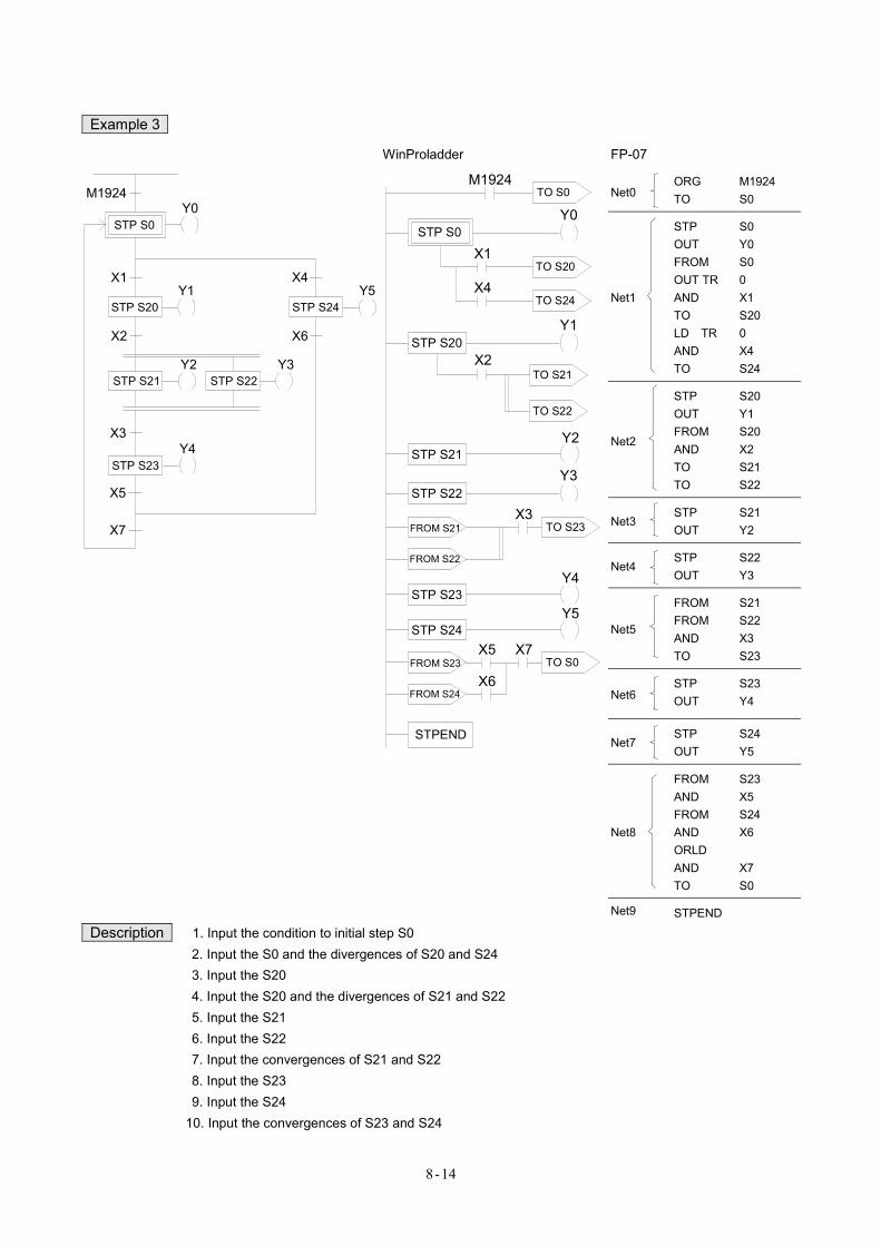
8-14
Example 3
WinProladder FP-07
Net0 ORG TO
M1924 S0
Net1
STP OUT FROM OUT TR AND TO LD TR AND TO
S0 Y0 S0 0 X1 S20 0 X4 S24
Net2
STP OUT FROM AND TO TO
S20 Y1 S20 X2 S21 S22
Net3 STP OUT
S21 Y2
Net4 STP OUT
S22 Y3
Net5
FROM FROM AND TO
S21 S22 X3 S23
Net6 STP OUT
S23 Y4
Net7 STP OUT
S24 Y5
Net8
FROM AND FROM AND ORLD AND TO
S23 X5 S24 X6 X7 S0
M1924
STP S0Y0
X1
STP S20Y1
Y3STP S22STP S21
Y2
STP S23
X5
X3Y4
X2
X7
X4
X6
STP S24Y5
M1924
STP S0
Y1
Y0
Y2
STPEND
X1
STP S20X2
STP S21
Y3STP S22
X3
Y4STP S23
X5
TO S20
TO S24
TO S21
TO S0
TO S23
FROM S22
FROM S21
X4
TO S22
Y5STP S24
X7TO S0
FROM S24
FROM S23
X6
Net9 STPEND
Description 1. Input the condition to initial step S0 2. Input the S0 and the divergences of S20 and S24 3. Input the S20 4. Input the S20 and the divergences of S21 and S22 5. Input the S21 6. Input the S22 7. Input the convergences of S21 and S22 8. Input the S23 9. Input the S24
10. Input the convergences of S23 and S24
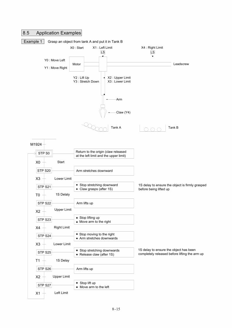
8-15
8.5 Application Examples
Example 1 Grasp an object from tank A and put it in Tank B
Tank A
Arm
Claw (Y4)
Tank B
Y0 : Move Left
Y1 : Move RightMotor
X0 : Start X1 : Left Limit
Y2 : Lift UpY3 : Stretch Down
X2 : Upper LimitX3 : Lower Limit
X4 : Right Limit
Leadscrew
LS LS
M1924
STP S0
X0
STP S20
T0
STP S22
X2
STP S23
X3
STP S21
T1
STP S26
X3
STP S25
X2
STP S27
X4
STP S24
X1
Start
Lower Limit
1S Delaly
Upper Limit
Right Limit
Lower Limit
1S Delay
Upper Limit
Left Limit
Return to the origin (claw releasedat the left limit and the upper limit)
Arm stretches downward
Stop stretching downwardClaw grasps (after 1S)
Arm lifts up
Stop moving to the rightArm stretches downwards
Stop lifting upMove arm to the right
Stop stretching downwardsRelease claw (after 1S)
Arm lifts up
Stop lift upMove arm to the left
1S delay to ensure the object is firmly graspedbefore being lifted up
1S delay to ensure the object has beencompletely released before lifting the arm up
8-16
WinProladder FP-07
M1924
STP S0
Y3
Y4
STPEND
STP S20
X0
X1
X3
T0
TO S21
TO S0
TO S22
STP S21
Y0
X2 Y2
SET Y4
T0 100
EN
EN
Y2STP S22
X2TO S23
Y1STP S23
X4TO S24
Y3STP S24
X3TO S25
T1TO S26
STP S25 EN
EN
Y2STP S26
X2TO S27
Y0STP S27
X1TO S0
RST Y4
T1 100
TO S20
Release claw
Return to the left limit
Return to the upper limit
Turn the switch ON before moving to S20
Stretch arm downward
Move to S21 after stretching to the lower limit
Claw grasps (since the SET instruction is used, Y4 should remain ON after departing from STP S21)
Divergent into S22 after 1S
Lift the arm up
Divergent into S23 after reaching the upper limit
Move arm to the right
Divergent into S24 after moving to the right limit
Stretch the arm downward
Divergent into S25 after stretching to the lower limit
Release claw
Delay for 1S
Transfer into S26 after 1S
Lift the arm up
Divergent into S27 after reaching the upper limit
Move the arm to the left
Divergent into S0 after moving to the left limit (a complete cycle)
ORG TO STP OUT TR OUT NOT AND NOT OUT LD TR AND NOT OUT FROM AND TO STP OUT FROM AND TO STP SET T0 PV: FROM AND TO STP OUT FROM AND TO STP OUT FROM AND TO STP OUT FROM AND TO STP RST T1 PV: FROM AND TO STP OUT FROM AND TO STP OUT FROM AND TO STPEND
M1924 S0 S0 0 Y4 X1 Y0 0 X2 Y2 S0 X0 S20 S20 Y3 S20 X3 S21 S21 Y4 100 S21 T0 S22 S22 Y2 S22 X2 S23 S23 Y1 S23 X4 S24 S24 Y3 S24 X3 S25 S25 Y4 100 S25 T1 S26 S26 Y2 S26 X2 S27 S27 Y0 S27 X1 S0
8-17
Example 2 Liquid Stirring Process
Weighing
Driedmaterial
Empty LimitSwitchX1
Value 1 Y5
CH0 : R3840
Value 1 Y6
Liquid
Value Y7
Stirring Unit
Value Y9
No Liquid LimitSwitchX2
Value 4 Y10
Clear Water
Finished ProductOutlet
StirringMotor
Y8Electromagnetic Switch
X4Overload Switch
Input Points: Empty limit switch X1 No liquid limit switch X2 Empty limit switch X3 Over-load switch X4 Warning clear button X5 Start button X6 Water washing button X7
Warning Indicators: Empty dried material Y1 Insufficient liquid Y2 Empty stirring unit Y3 Motor over-load Y4
Output Points: Dried material inlet valve Y5 Dried material inlet valve Y6 Liquid inlet valve Y7 Motor start electromagnetic valve Y8 Clean water inlet valve Y9 Finished product outlet valve Y10
Weighing Output: CH0(R3840)
M1918=0
Clean Water
8-18
WinProladder FP-07
ORG M1924 STP S22
TO S0 OUT Y7 STP S0 T1 PV: 800 OUT TR 0 FROM S21 AND NOT X1 FROM S22 SET Y1 AND T0 LD TR 0 AND T1 AND NOT X2 TO S23 SET Y2 STP S23 LD TR 0 OUT TR 0 AND X3 OUT Y8 SET Y3 LD TR 0 LD TR 0 T2 PV: 4500 AND X4 LD TR 0 SET Y4 AND X4 LD TR 0 OUT Y4 AND X5 STP S24 RST Y1 OUT TR 0 RST Y2 T3 PV: 500 RST Y3 LD TR 0 RST Y4 AND NOT T3 FROM S0 OUT Y9 OUT TR 1 LD TR 0 AND X6 T4 PV: 1500 AND NOT Y1 LD TR 0 AND NOT Y2 AND NOT T4 AND NOT Y3 OUT Y10 AND NOT Y4 FROM S23 TO S20 AND T2 LD TR 1 FROM S24 AND X7 AND T4 AND NOT Y3 ORLD AND NOT Y4 TO S25 TO S24 STP S25 STP S20 OUT TR 0 OUT Y5 AND X3 FUN 17 OUT Y10
Sa:R3840 LD TR 0 Sb:R0 AND TU S25
FO 0 FUN 15DP OUT M0 D:R10 FO 1 FROM S25 OUT M1 AND NOT X3 FROM S20 TO S0 LD M0 STPEND OR M1 ANDLD TO S21 TO S22 STP S21 OUT Y6
M1924
STP S0
STPEND
STP S21
X3
M0
TO S20
TO S0
TO S21
STP S20
X2
X1SET Y1
SET Y2
SET Y3
X5
X4SET Y4
RST Y1
RST Y2
RST Y3
RST Y4Y4Y3Y2Y1X6
TO S24Y4Y3
Y5
M0
Sb : R0
Sa : R384017CMP
M1
M1TO S22
Y6
EN T0 500
STP S22Y7
EN T1 800
FROM S21 TO S23T0 T1
FROM S22
STP S23Y8
EN T2 4500
Y4X4
STP S24 EN T3 500
Y9T3
EN T4 1500
Y10T4
FROM S23 TO S25T2
FROM S24T4
STP S25
+1 R10
Y10
X3
X3
S25
TO S0
15DP
X7
Warning indicators
Reset warning
Production start
Water washing start
Input weighing
Status after weighing
Divergent into S21 and S22
Input material to stirring unit
Add liquid to stirring unit
Complete dried material and liquid input, transfer the status to S23
Stirring timer
Wash stirring unit
Input clean water
Drain water out
Output finished product and accumulate the cycle
T0 PV: 500
8-19
Example 3 Pedestrian Crossing Lights
Y4 (Green)
Y3 (Red)Y0 (Red)Y1 (Amber)Y2 (Green)
Y4(Green)
X0
X1
Input Points: Pedestrian Push Button X0 Pedestrian Push Button X1
Output Points: Road Red Light Y0 Road Amber light Y1 Road Green Light Y2 Pedestrian Crossing Red Light Y3 Pedestrian Crossing Green Light Y4
M1918=0
Y3 (Red)
Y4 (Green)
X1
Y0 (Red) Y1 (Amber) Y2 (Green)
Y4 (Green)
X0
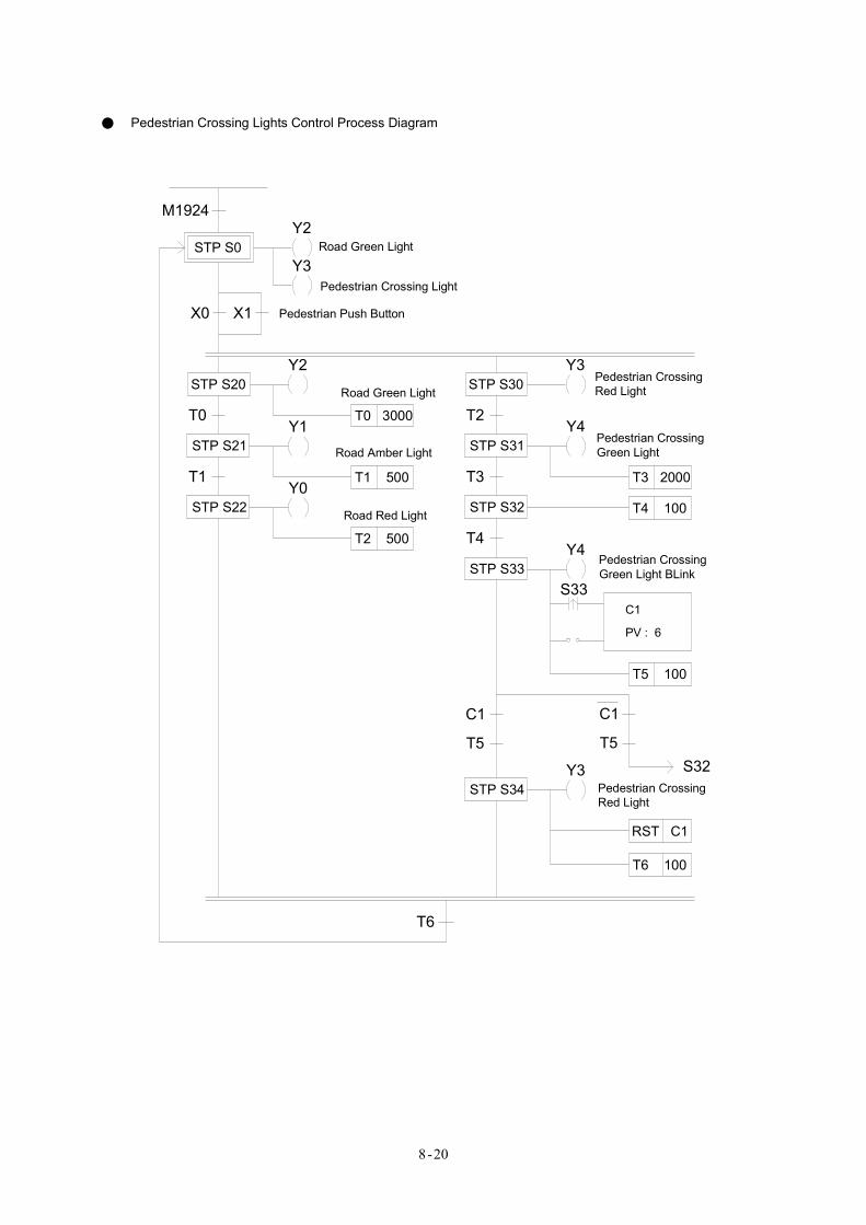
8-20
● Pedestrian Crossing Lights Control Process Diagram
Y2M1924
STP S0
X0
T6
STP S20
STP S21
STP S22
T1
Y3
X1
T0
Y2
Y1
Y0
T0 3000
T1 500
T2 500
STP S30
STP S31
STP S32
T3
T2
Y3
Y4
T3 2000
T4 100
Road Green Light
Road Amber Light
Road Red Light
T4
STP S33Y4
PV : 6
C1S33
C1
T5
STP S34Y3
RST C1
T6 100
Road Green Light
Pedestrian Push Button
Pedestrian Crossing Light
Pedestrian CrossingRed Light
Pedestrian CrossingGreen Light
Pedestrian CrossingGreen Light BLink
C1
T5S32
Pedestrian CrossingRed Light
T5 100
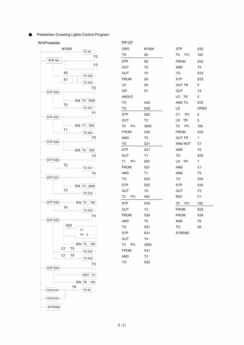
8-21
● Pedestrian Crossing Lights Control Program
WinProladder FP-07 ORG
TO
M1924
S0
STP
T4 PV:
S32
100
STP
OUT
OUT
S0
Y2
Y3
FROM
AND
TO
S32
T4
S33
FROM
LD
OR
ANDLD
TO
TO
S0
X0
X1
S20
S30
STP
OUT TR
OUT
LD TR
AND TU
LD
S33
0
Y4
0
S33
OPEN
STP
OUT
T0 PV:
FROM
AND
TO
S20
Y2
3000
S20
T0
S21
C1 PV:
LD TR
T5 PV:
FROM
OUT TR
AND NOT
6
0
100
S33
1
C1
STP
OUT
T1 PV:
FROM
AND
TO
S21
Y1
500
S21
T1
S22
AND
TO
LD TR
AND
AND
TO
T5
S32
1
C1
T5
S34
STP
OUT
T2 PV:
S22
Y0
500
STP
OUT
RST
S34
Y3
C1
STP S30 T6 PV: 100
OUT
FROM
AND
TO
Y3
S30
T2
S31
FROM
FROM
AND
TO
S22
S34
T6
S0
TO S30
EN T0 3000
T1TO S22
STP S21Y1
EN T1 500
STP S22Y0
EN T2 500
T2TO S31
T3TO S32
STP S31Y4
EN T3 2000
STP S32
T4TO S33
EN T4 100
C1TO S32
STP S33Y4
PV : 6
C1
C1TO S34
S33
EN T5 100T5
T5
EN T6 100
M1924
STP S0
STPEND
STP S30
T0
TO S0
TO S21
STP S20Y2
Y3
STP S34Y3
RST C1
FROM S22 TO S0T6
FROM S34
Y2
Y3
X0TO S20
X1
STP
OUT
T3 PV:
FROM
AND
TO
S31
Y4
2000
S31
T3
S32
STPEND
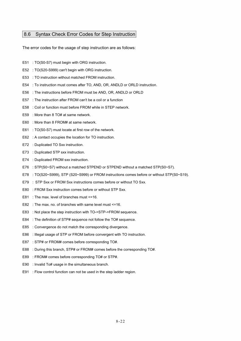
8-22
8.6 Syntax Check Error Codes for Step Instruction
The error codes for the usage of step instruction are as follows:
E51 : TO(S0-S7) must begin with ORG instruction.
E52 : TO(S20-S999) can't begin with ORG instruction.
E53 : TO instruction without matched FROM instruction.
E54 : To instruction must comes after TO, AND, OR, ANDLD or ORLD instruction.
E56 : The instructions before FROM must be AND, OR, ANDLD or ORLD
E57 : The instruction after FROM can't be a coil or a function
E58 : Coil or function must before FROM while in STEP network.
E59 : More than 8 TO# at same network.
E60 : More than 8 FROM# at same network.
E61 : TO(S0-S7) must locate at first row of the network.
E62 : A contact occupies the location for TO instruction.
E72 : Duplicated TO Sxx instruction.
E73 : Duplicated STP sxx instruction.
E74 : Duplicated FROM sxx instruction.
E76 : STP(S0~S7) without a matched STPEND or STPEND without a matched STP(S0~S7).
E78 : TO(S20~S999), STP (S20~S999) or FROM instructions comes before or without STP(S0~S19).
E79 : STP Sxx or FROM Sxx instructions comes before or without TO Sxx.
E80 : FROM Sxx instruction comes before or without STP Sxx.
E81 : The max. level of branches must <=16.
E82 : The max. no. of branches with same level must <=16.
E83 : Not place the step instruction with TO->STP->FROM sequence.
E84 : The definition of STP# sequence not follow the TO# sequence.
E85 : Convergence do not match the corresponding divergence.
E86 : Illegal usage of STP or FROM before convergent with TO instruction.
E87 : STP# or FROM# comes before corresponding TO#.
E88 : During this branch, STP# or FROM# comes before the corresponding TO#.
E89 : FROM# comes before corresponding TO# or STP#.
E90 : Invalid To# usage in the simultaneous branch.
E91 : Flow control function can not be used in the step ladder region.
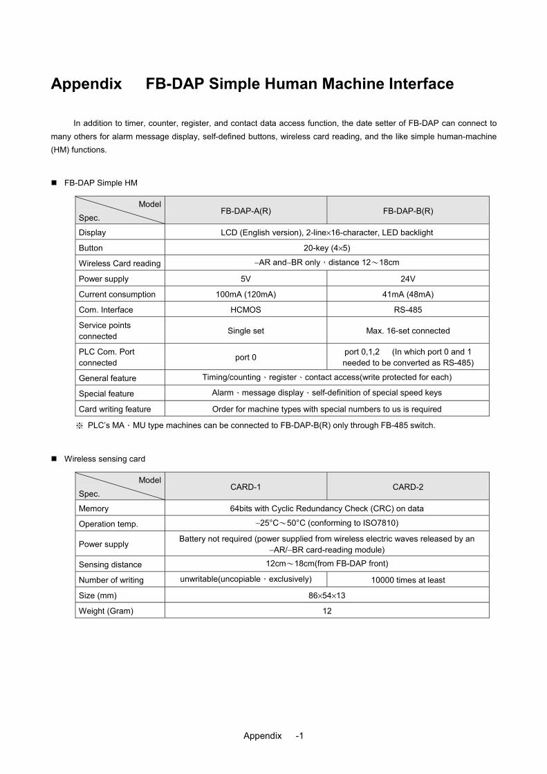
Appendix -1
Appendix FB-DAP Simple Human Machine Interface
In addition to timer, counter, register, and contact data access function, the date setter of FB-DAP can connect to many others for alarm message display, self-defined buttons, wireless card reading, and the like simple human-machine (HM) functions.
FB-DAP Simple HM
ModelSpec.
FB-DAP-A(R) FB-DAP-B(R)
Display LCD (English version), 2-line×16-character, LED backlight
Button 20-key (4×5)
Wireless Card reading −AR and−BR only,distance 12~18cm
Power supply 5V 24V
Current consumption 100mA (120mA) 41mA (48mA)
Com. Interface HCMOS RS-485
Service points connected
Single set Max. 16-set connected
PLC Com. Port connected
port 0 port 0,1,2 (In which port 0 and 1 needed to be converted as RS-485)
General feature Timing/counting、register、contact access(write protected for each)
Special feature Alarm、message display、self-definition of special speed keys
Card writing feature Order for machine types with special numbers to us is required
※ PLC’s MA、MU type machines can be connected to FB-DAP-B(R) only through FB-485 switch.
Wireless sensing card
ModelSpec.
CARD-1 CARD-2
Memory 64bits with Cyclic Redundancy Check (CRC) on data
Operation temp. −25°C~50°C (conforming to ISO7810)
Power supply Battery not required (power supplied from wireless electric waves released by an −AR/−BR card-reading module)
Sensing distance 12cm~18cm(from FB-DAP front)
Number of writing unwritable(uncopiable,exclusively) 10000 times at least
Size (mm) 86×54×13
Weight (Gram) 12
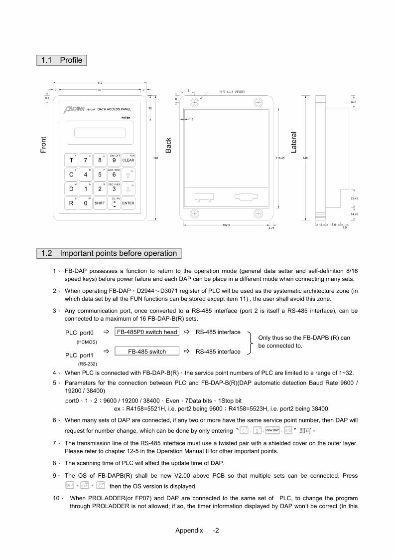
Appendix -2
1.1 Profile
R
D
C
T
6.5
7
ENTER
5
2
SHIFT0
1
4M
S
Y
A
W
E
3
6ADR / DOC
CV / PV
DEC / HEXB
F
CLEAR87X +
9ON / OFF FUN
7
9.9
14.75
22.43
DATA ACCESS PANEL
12102.54.75
8
1.5
16
118.45 148
98
112
148
30
17.6
外徑 4ψ×4 埋螺帽
14.8
Bac
k
Fron
t
FB-DAP
FATEK
Late
ral
1.2 Important points before operation
1、 FB-DAP possesses a function to return to the operation mode (general data setter and self-definition 8/16 speed keys) before power failure and each DAP can be place in a different mode when connecting many sets.
2、 When operating FB-DAP,D2944~D3071 register of PLC will be used as the systematic architecture zone (in which data set by all the FUN functions can be stored except item 11) , the user shall avoid this zone.
3、 Any communication port, once converted to a RS-485 interface (port 2 is itself a RS-485 interface), can be connected to a maximum of 16 FB-DAP-B(R) sets.
FB-485P0 switch head RS-485 interface FB-485 switch RS-485 interface
Only thus so the FB-DAPB (R) can be connected to.
PLC port0 (HCMOS)
PLC port1 (RS-232)
4、 When PLC is connected with FB-DAP-B(R),the service point numbers of PLC are limited to a range of 1~32.
5、 Parameters for the connection between PLC and FB-DAP-B(R)(DAP automatic detection Baud Rate 9600 / 19200 / 38400)
port0、1、2:9600 / 19200 / 38400、Even、7Data bits、1Stop bit ex:R4158=5521H, i.e. port2 being 9600;R4158=5523H, i.e. port2 being 38400.
6、 When many sets of DAP are connected, if any two or more have the same service point number, then DAP will
request for number change, which can be done by only entering〝 new DAP 〞即可。
7、 The transmission line of the RS-485 interface must use a twisted pair with a shielded cover on the outer layer. Please refer to chapter 12-5 in the Operation Manual II for other important points.
8、 The scanning time of PLC will affect the update time of DAP.
9、 The OS of FB-DAPB(R) shall be new V2.00 above PCB so that multiple sets can be connected. Press
then the OS version is displayed.
10、 When PROLADDER(or FP07) and DAP are connected to the same set of PLC, to change the program through PROLADDER is not allowed; if so, the timer information displayed by DAP won’t be correct (In this
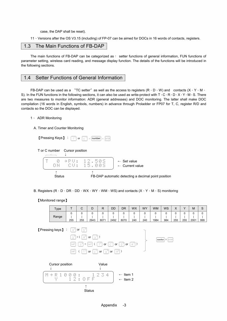
Appendix -3
case, the DAP shall be reset).
11、 Versions after the OS V3.15 (including) of FP-07 can be aimed for DOCs in 16 words of contacts, registers.
1.3 The Main Functions of FB-DAP
The main functions of FB-DAP can be categorized as: setter functions of general information, FUN functions of parameter setting, wireless card reading, and message display function. The details of the functions will be introduced in the following sections.
1.4 Setter Functions of General Information
FB-DAP can be used as a 〝TC setter〞as well as the access to registers (R、D、W) and contacts (X、Y、M、
S). In the FUN functions in the following sections, it can also be used as write-protect with T、C、R、D、X、Y、M、S. There are two measures to monitor information: ADR (general addresses) and DOC monitoring. The latter shall make DOC compilation (16 words in English, symbols, numbers) in advance through Proladder or FP07 for T, C, register R/D and contacts so the DOC can be displayed.
1、 ADR Monitoring
A. Timer and Counter Monitoring
【Pressing Keys】: or number
T or C number Cursor position ↓
← Set value ← Current value
↑ ↑ Status FB-DAP automatic detecting a decimal point position
B. Registers (R、D、DR、DD、WX、WY、WM、WS) and contacts (X、Y、M、S) monitoring
【Monitored range】
Type T C D R DD DR WX WY WM WS X Y M S
Range 0 |
255
0 |
255
0 |
2943
0 |
8071
0 |
2492
0 |
8070
0 |
240
0 |
240
0 |
1984
0 |
984
0 |
255
0 |
255
0 |
2001
0 |
999
【Pressing keys】:
+
(
(
+ ( )
)
)
or
or
or or or
or or or
number +
Cursor position Value ↓ ↓
← Item 1 ← Item 2
↑ Status
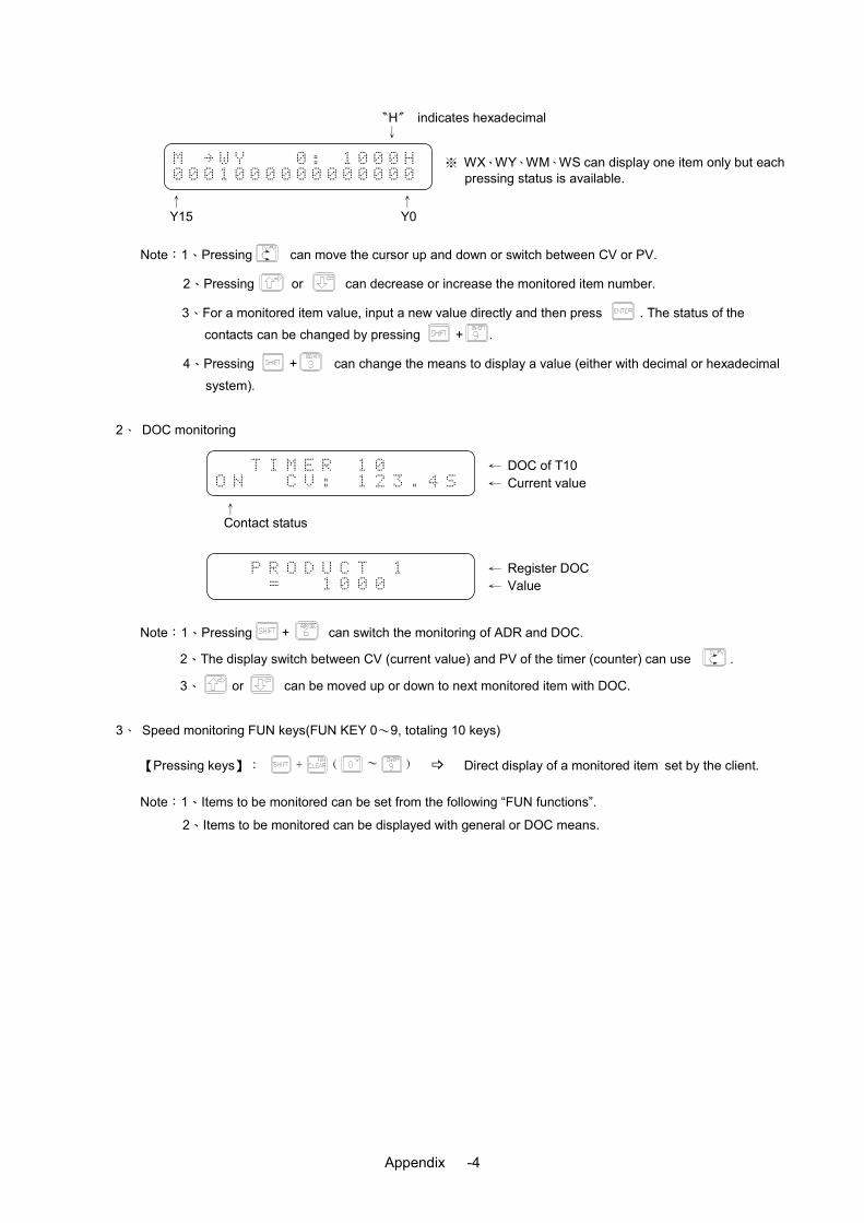
Appendix -4
〝H〞 indicates hexadecimal ↓
※ WX、WY、WM、WS can display one item only but each pressing status is available.
↑ ↑ Y15 Y0
Note:1、Pressing can move the cursor up and down or switch between CV or PV.
2、Pressing or can decrease or increase the monitored item number.
3、For a monitored item value, input a new value directly and then press . The status of the
contacts can be changed by pressing + .
4、Pressing + can change the means to display a value (either with decimal or hexadecimal
system).
2、 DOC monitoring
← DOC of T10 ← Current value
↑ Contact status
← Register DOC ← Value
Note:1、Pressing + can switch the monitoring of ADR and DOC.
2、The display switch between CV (current value) and PV of the timer (counter) can use .
3、 or can be moved up or down to next monitored item with DOC.
3、 Speed monitoring FUN keys(FUN KEY 0~9, totaling 10 keys)
【Pressing keys】: + ( ~ ) Direct display of a monitored item set by the client.
Note:1、Items to be monitored can be set from the following “FUN functions”.
2、Items to be monitored can be displayed with general or DOC means.
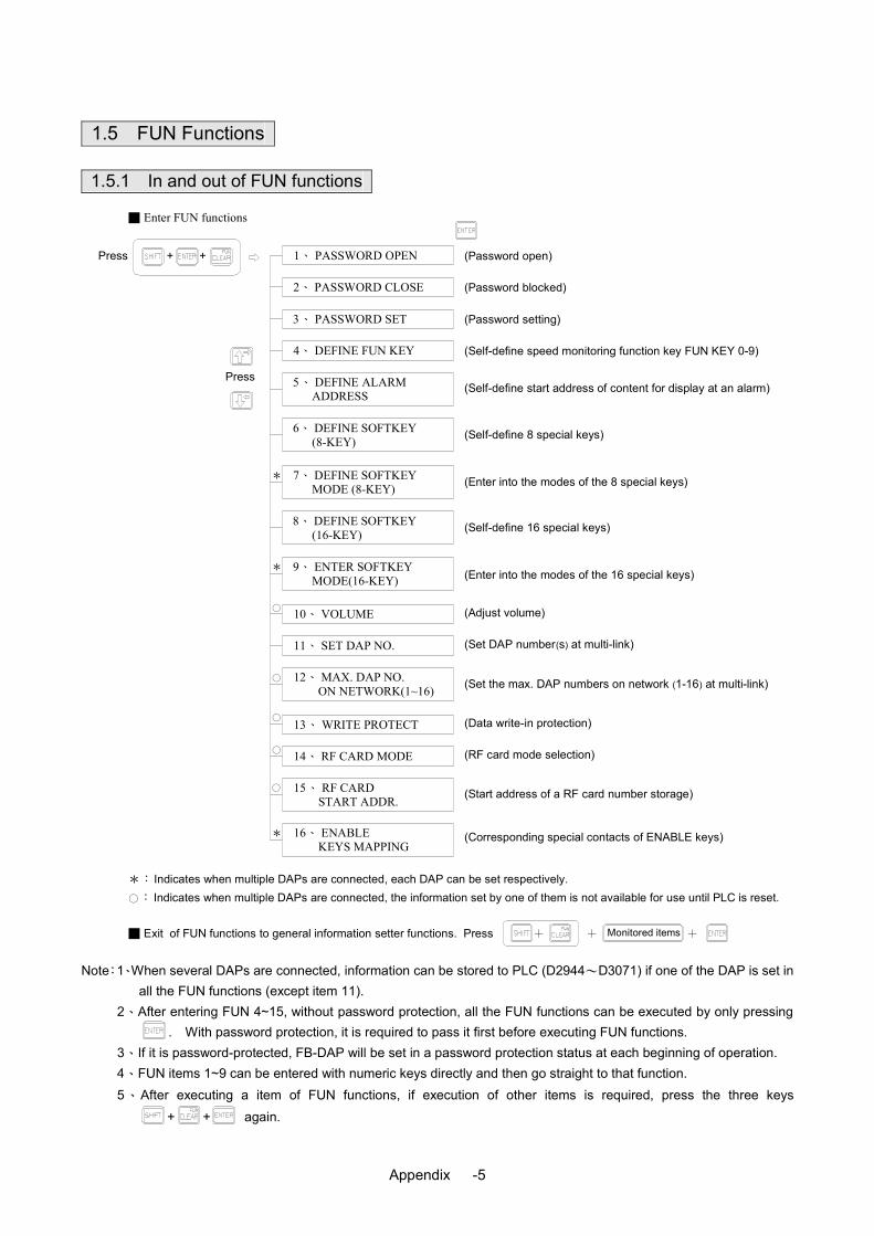
Appendix -5
1.5 FUN Functions
1.5.1 In and out of FUN functions
Note:1、When several DAPs are connected, information can be stored to PLC (D2944~D3071) if one of the DAP is set in all the FUN functions (except item 11).
2、After entering FUN 4~15, without password protection, all the FUN functions can be executed by only pressing . With password protection, it is required to pass it first before executing FUN functions.
3、If it is password-protected, FB-DAP will be set in a password protection status at each beginning of operation. 4、FUN items 1~9 can be entered with numeric keys directly and then go straight to that function. 5、After executing a item of FUN functions, if execution of other items is required, press the three keys
+ + again.
16、 ENABLE KEYS MAPPING
13、 WRITE PROTECT
14、 RF CARD MODE
15、 RF CARD START ADDR.
11、 SET DAP NO.
12、 MAX. DAP NO. ON NETWORK(1~16)
9、 ENTER SOFTKEY MODE(16-KEY)
7、 DEFINE SOFTKEY MODE (8-KEY)
8、 DEFINE SOFTKEY (16-KEY)
6、 DEFINE SOFTKEY (8-KEY)
5、 DEFINE ALARM ADDRESS
3、 PASSWORD SET
4、 DEFINE FUN KEY
2、 PASSWORD CLOSE
1、 PASSWORD OPEN
*: Indicates when multiple DAPs are connected, each DAP can be set respectively. ○ : Indicates when multiple DAPs are connected, the information set by one of them is not available for use until PLC is reset.
■ Exit of FUN functions to general information setter functions. Press + + +
*
○
○
○
○
○ 10、 VOLUME
*
*
Press + +
■ Enter FUN functions
Press
(Self-define 8 special keys)
(RF card mode selection)
(Start address of a RF card number storage)
(Corresponding special contacts of ENABLE keys)
Monitored items
(Enter into the modes of the 8 special keys)
(Enter into the modes of the 16 special keys)
(Set DAP number(s) at multi-link)
(Set the max. DAP numbers on network (1-16) at multi-link)
(Adjust volume)
(Data write-in protection)
(Self-define 16 special keys)
(Self-define speed monitoring function key FUN KEY 0-9)
(Self-define start address of content for display at an alarm)
(Password blocked)
(Password setting)
(Password open)
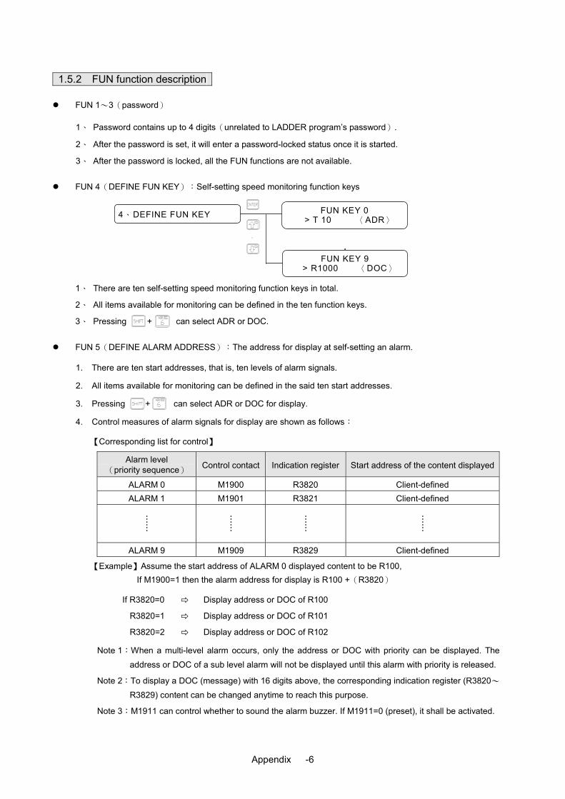
Appendix -6
1.5.2 FUN function description
FUN 1~3(password)
1、 Password contains up to 4 digits(unrelated to LADDER program’s password).
2、 After the password is set, it will enter a password-locked status once it is started.
3、 After the password is locked, all the FUN functions are not available.
FUN 4(DEFINE FUN KEY):Self-setting speed monitoring function keys
1、 There are ten self-setting speed monitoring function keys in total.
2、 All items available for monitoring can be defined in the ten function keys.
3、 Pressing + can select ADR or DOC.
FUN 5(DEFINE ALARM ADDRESS):The address for display at self-setting an alarm.
1. There are ten start addresses, that is, ten levels of alarm signals.
2. All items available for monitoring can be defined in the said ten start addresses.
3. Pressing + can select ADR or DOC for display.
4. Control measures of alarm signals for display are shown as follows:
【Corresponding list for control】
Alarm level (priority sequence) Control contact Indication register Start address of the content displayed
ALARM 0 M1900 R3820 Client-defined ALARM 1 M1901 R3821 Client-defined
……
……
……
……
ALARM 9 M1909 R3829 Client-defined
【Example】Assume the start address of ALARM 0 displayed content to be R100, If M1900=1 then the alarm address for display is R100 +(R3820)
If R3820=0 Display address or DOC of R100
R3820=1 Display address or DOC of R101
R3820=2 Display address or DOC of R102
Note 1:When a multi-level alarm occurs, only the address or DOC with priority can be displayed. The
address or DOC of a sub level alarm will not be displayed until this alarm with priority is released.
Note 2:To display a DOC (message) with 16 digits above, the corresponding indication register (R3820~
R3829) content can be changed anytime to reach this purpose.
Note 3:M1911 can control whether to sound the alarm buzzer. If M1911=0 (preset), it shall be activated.
…
、
4、DEFINE FUN KEY FUN KEY 0 > T 10 〈ADR〉
FUN KEY 9 > R1000 〈DOC〉
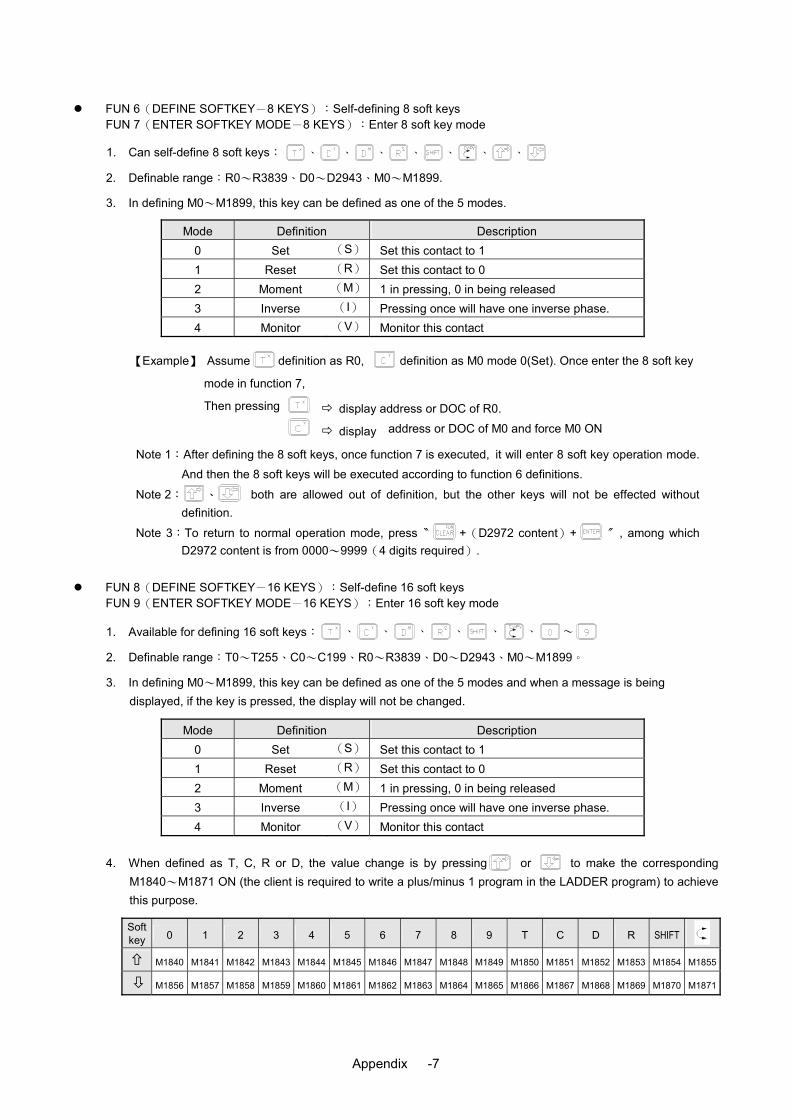
Appendix -7
FUN 6(DEFINE SOFTKEY-8 KEYS):Self-defining 8 soft keys FUN 7(ENTER SOFTKEY MODE-8 KEYS):Enter 8 soft key mode
1. Can self-define 8 soft keys: 、 、 、 、、 、 、
2. Definable range:R0~R3839、D0~D2943、M0~M1899.
3. In defining M0~M1899, this key can be defined as one of the 5 modes.
Mode Definition Description 0 Set (S) Set this contact to 1 1 Reset (R) Set this contact to 0 2 Moment (M) 1 in pressing, 0 in being released 3 Inverse (I) Pressing once will have one inverse phase. 4 Monitor (V) Monitor this contact
【Example】 Assume definition as R0, definition as M0 mode 0(Set). Once enter the 8 soft key
mode in function 7,
Then pressing display address or DOC of R0.
display address or DOC of M0 and force M0 ON
Note 1:After defining the 8 soft keys, once function 7 is executed, it will enter 8 soft key operation mode. And then the 8 soft keys will be executed according to function 6 definitions.
Note 2: 、 both are allowed out of definition, but the other keys will not be effected without definition.
Note 3:To return to normal operation mode, press〝 +(D2972 content)+ 〞, among which D2972 content is from 0000~9999(4 digits required).
FUN 8(DEFINE SOFTKEY-16 KEYS):Self-define 16 soft keys FUN 9(ENTER SOFTKEY MODE-16 KEYS):Enter 16 soft key mode
1. Available for defining 16 soft keys: 、 、 、 、、 、 ~
2. Definable range:T0~T255、C0~C199、R0~R3839、D0~D2943、M0~M1899。
3. In defining M0~M1899, this key can be defined as one of the 5 modes and when a message is being displayed, if the key is pressed, the display will not be changed.
Mode Definition Description 0 Set (S) Set this contact to 1 1 Reset (R) Set this contact to 0 2 Moment (M) 1 in pressing, 0 in being released 3 Inverse (I) Pressing once will have one inverse phase. 4 Monitor (V) Monitor this contact
4. When defined as T, C, R or D, the value change is by pressing or to make the corresponding M1840~M1871 ON (the client is required to write a plus/minus 1 program in the LADDER program) to achieve this purpose.
Soft key 0 1 2 3 4 5 6 7 8 9 T C D R SHIFT
M1840 M1841 M1842 M1843 M1844 M1845 M1846 M1847 M1848 M1849 M1850 M1851 M1852 M1853 M1854 M1855
M1856 M1857 M1858 M1859 M1860 M1861 M1862 M1863 M1864 M1865 M1866 M1867 M1868 M1869 M1870 M1871
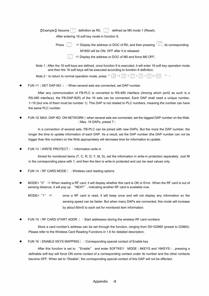
Appendix -8
【Example】Assume definition as R0, defined as M0 mode 1 (Reset).
After entering 16 soft key mode in function 9,
Press Display the address or DOC of R0, and then pressing , its corresponding
M1850 will be ON; OFF after it is released.
Display the address or DOC of M0 and force M0 OFF.
Note 1:After the 16 soft keys are defined, once function 9 is executed, it will enter 16 soft key operation mode and then the 16 soft keys will be executed according to function 8 definition.
Note 2:to return to normal operation mode, press〝 + ( + + + ) + 〞。
FUN 11(SET DAP NO.):When several sets are connected, set DAP number.
After any communication of FB-PLC is converted to RS-485 interface (Among which port2 as such is a RS-485 interface), the FB-DAP-B(R) of the 16 sets can be connected. Each DAP shall need a unique number, 1~16 (but one of them must be number 1). This DAP is not related to PLC numbers, meaning the number can have the same PLC number.
FUN 12(MAX. DAP NO. ON NETWORK):when several sets are connected, set the biggest DAP number on the Web. (Max. 16 DAPs, preset 7)
In a connection of several sets, FB-PLC can be joined with new DAPs. But the more the DAP number, the longer the time to update information of each DAP. As a result, set the DAP number (the DAP number can not be bigger than this number) on the Web appropriately will decrease time for information to update.
FUN 13(WRITE PROTECT):Information write in
Aimed for monitored items (T, C, R, D, Y, M, S), set the information in write-in protection separately. Just fill in the corresponding place with 1, and then the item is write-in protected and can be read values only.
FUN 14(RF CARD MODE):Wireless card reading options
MODE=〝0〞 When reading a RF card, it will display whether this card is OK or Error. When the RF card is out of sensing distance, it will pop up 〝NEXT〞, indicating another RF card is available now.
MODE=〝1〞 once a RF card is read, it will beep once and will not display any information so the
sensing speed can be faster. But when many DAPs are connected, this mode will increase
by about 60mS to each set for monitored item information.
FUN 15(RF CARD START ADDR.):Start addresses storing the wireless RF card numbers
Store a card number’s address can be set through the function, ranging from D0~D2860 (preset to D2860). Please refer to the Wireless Card Reading Functions in 1.6 for detailed description.
FUN 16(ENABLE KEYS MAPPING):Corresponding special contact of Enable key
After this function is set to 〝Enable〞 and enter SOFTKEY MODE(8KEYS and 16KEYS), pressing a definable soft key will force ON some contact of a corresponding contact under its number and the other contacts become OFF. When set to “Disable”, the corresponding special contact of this DAP will not be effected.
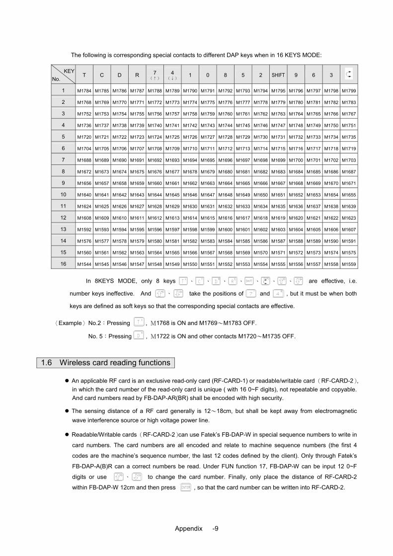
Appendix -9
The following is corresponding special contacts to different DAP keys when in 16 KEYS MODE:
KEY No.
T C D R 7 (↑)
4 (↓)
1 0 8 5 2 SHIFT 9 6 3
1 M1784 M1785 M1786 M1787 M1788 M1789 M1790 M1791 M1792 M1793 M1794 M1795 M1796 M1797 M1798 M1799
2 M1768 M1769 M1770 M1771 M1772 M1773 M1774 M1775 M1776 M1777 M1778 M1779 M1780 M1781 M1782 M1783
3 M1752 M1753 M1754 M1755 M1756 M1757 M1758 M1759 M1760 M1761 M1762 M1763 M1764 M1765 M1766 M1767
4 M1736 M1737 M1738 M1739 M1740 M1741 M1742 M1743 M1744 M1745 M1746 M1747 M1748 M1749 M1750 M1751
5 M1720 M1721 M1722 M1723 M1724 M1725 M1726 M1727 M1728 M1729 M1730 M1731 M1732 M1733 M1734 M1735
6 M1704 M1705 M1706 M1707 M1708 M1709 M1710 M1711 M1712 M1713 M1714 M1715 M1716 M1717 M1718 M1719
7 M1688 M1689 M1690 M1691 M1692 M1693 M1694 M1695 M1696 M1697 M1698 M1699 M1700 M1701 M1702 M1703
8 M1672 M1673 M1674 M1675 M1676 M1677 M1678 M1679 M1680 M1681 M1682 M1683 M1684 M1685 M1686 M1687
9 M1656 M1657 M1658 M1659 M1660 M1661 M1662 M1663 M1664 M1665 M1666 M1667 M1668 M1669 M1670 M1671
10 M1640 M1641 M1642 M1643 M1644 M1645 M1646 M1647 M1648 M1649 M1650 M1651 M1652 M1653 M1654 M1655
11 M1624 M1625 M1626 M1627 M1628 M1629 M1630 M1631 M1632 M1633 M1634 M1635 M1636 M1637 M1638 M1639
12 M1608 M1609 M1610 M1611 M1612 M1613 M1614 M1615 M1616 M1617 M1618 M1619 M1620 M1621 M1622 M1623
13 M1592 M1593 M1594 M1595 M1596 M1597 M1598 M1599 M1600 M1601 M1602 M1603 M1604 M1605 M1606 M1607
14 M1576 M1577 M1578 M1579 M1580 M1581 M1582 M1583 M1584 M1585 M1586 M1587 M1588 M1589 M1590 M1591
15 M1560 M1561 M1562 M1563 M1564 M1565 M1566 M1567 M1568 M1569 M1570 M1571 M1572 M1573 M1574 M1575
16 M1544 M1545 M1546 M1547 M1548 M1549 M1550 M1551 M1552 M1553 M1554 M1555 M1556 M1557 M1558 M1559
In 8KEYS MODE, only 8 keys 、 、 、 、 、 、 、 are effective, i.e.
number keys ineffective. And 、 take the positions of and , but it must be when both
keys are defined as soft keys so that the corresponding special contacts are effective.
〈Example〉 No.2:Pressing , M1768 is ON and M1769~M1783 OFF.
No. 5:Pressing , M1722 is ON and other contacts M1720~M1735 OFF.
1.6 Wireless card reading functions
An applicable RF card is an exclusive read-only card (RF-CARD-1) or readable/writable card (RF-CARD-2), in which the card number of the read-only card is unique ( with 16 0~F digits), not repeatable and copyable. And card numbers read by FB-DAP-AR(BR) shall be encoded with high security.
The sensing distance of a RF card generally is 12~18cm, but shall be kept away from electromagnetic wave interference source or high voltage power line.
Readable/Writable cards (RF-CARD-2)can use Fatek’s FB-DAP-W in special sequence numbers to write in
card numbers. The card numbers are all encoded and relate to machine sequence numbers (the first 4
codes are the machine’s sequence number, the last 12 codes defined by the client). Only through Fatek’s
FB-DAP-A(B)R can a correct numbers be read. Under FUN function 17, FB-DAP-W can be input 12 0~F
digits or use 、 to change the card number. Finally, only place the distance of RF-CARD-2
within FB-DAP-W 12cm and then press , so that the card number can be written into RF-CARD-2.
Appendix -10
Locations and application of the card number storage
FB-DAP saves RF card numbers within sensing distance into two places in PLC. The places and application are described as follows:
4、Fixed in R3835~R3839(totaling 5 registers):During operation, M1910 shall be controlled.
Card number
format
R3835 N1 N2 R3836 × × × × R3837 × × × × R3838 × × × × R3839 × × × ×
N1:DAP number 1~16(i.e. 1H~10H)
N2:52H(R:read-only card) or 57H(W:readable/writable card)
R3836~R3839 store 16 0~F card numbers
Application: Only in monitoring (or8/16 soft keys) mode (non-FUN functions) and the RF card in sensing distance, FB-DAP(−AR or −BR)will send the RF card number together with DAP number to PLC R3835~R3839. In mode 0 of function 14 (RF CARD MODE), all the client needs to do is compare the card number. If it is OK, only set M1910 to 1 and then DAP will indicate “OK”, or “ERROR”. When the RF card is out of sensing distance, DAP will pop up “NEXT” and clear the content of PLC R3838~R3839 to 0, which means available for another RF card. In mode 1 of function 14, as soon as DAP reads a card number, it will save it to R3835~R3839 with a beep. After the RF card exits, the 5 registers remain unchanged.
Applicable occasions: Where one set or multiple sets are connected but RF cards are not used frequently, the program to be applied will be a lot easier. But in the event of a card number read from different DAPs at the same time, it will be difficult for PLC to identify the information correctly.
5、Preset D2860~D2939 (16 differently-located DAP take on 5 registers individually, i.e. 80 registers in all, but the locations can be changed through function 15) control one point of M1880~M1895 separately when in use.
Card number
format Card number format Card number
format Card number format
D2860 N1 N2 D2865 N1 N2 D2870 N1 N2 D2935 N1 N2 D2861 × × × × D2866 × × × × D2871 × × × × D2936 × × × × D2862 × × × × D2867 × × × × D2872 × × × × ……….. D2937 × × × × D2863 × × × × D2868 × × × × D2873 × × × × D2938 × × × × D2864 × × × × D2869 × × × × D3974 × × × × D2939 × × × ×
No. 1 ⇓
M1880
No. 2 ⇓
M1881
No. 3 ⇓
M1882
No. 16 ⇓
M1895
Application measures: The application measures are all described as the above-mentioned but that the storage places of card numbers and corresponding contacts for control are different. For example, in mode 0 of function 14, from No. 2 DAP sensing to the RF card, now no. 2 will send same card numbers to two different places in R3835~R3839 and D2865~D2869 (the content of the other registers remains unchanged), and all the client needs to do is control M1881 for the DAP to display “OK” or “ERROR”. After the RF card exits, the content of the 10 registers R3835~R3839 and D2865~D2869 will be cleared to 0 (but remains unchanged in mode 1).
Applicable occasions: When several DAPs are connected, the RF card can be read in from different DAPs and each DAP has its independent card numbers storage places and control points so that no PLC misjudgment case occurs, but the programming will be more troublesome.
※ If you do not want R3835~R3839 to display a card number value, you can use the Ladder program to fill in these registers with other fixed values.
Appendix -11
1.7 Special message display function
In general monitoring mode and soft key mode (16 KEYS or 8 KEYS), the user can configure the DAP to display every kind of message under some circumstances, and the two-line display on the LCD can be controlled separately to simultaneously display different messages. Every message is 1~511 words and numbers (ASCII code) long, in which a maximum of 16 variables (if variables with 32-digit are not used, then it can use up to 25) can be included. When a message has more than 16 words, the message will be displaced left for display, in which the moving speed or pause time can be configured flexibly.
1.7.1 Message display application
The FB-DAPB(R) can be connected up to 16 sets (Number 1~16). Each DAP not only can display different messages individually but make all the DAPs connected display the same message simultaneously. If you go to a special contact (R3780~M3813) set by Enable, the DAP will display the message ASCII Code) indicated by the corresponding indication register (R3780~M3813). The content of the indication register is the start register of messages, i.e. start of ASCII Code. The indication register content can be changed anytime in order to change and display different messages.
The following is a list of corresponding special contacts and indication registers when each DAP is displaying a message for control.
LCD line 1 LCD line 2 Number of a message displayed
Special contact
Indication register
Special contact
Indication register
1~16 M1800 R3780 M1801 R3781
1 M1802 R3782 M1803 R3783
2 M1804 R3784 M1805 R3785
3 M1806 R3786 M1807 R3787
4 M1808 R3788 M1809 R3789
5 M1810 R3790 M1811 R3791
6 M1812 R3792 M1813 R3793
7 M1814 R3794 M1815 R3795
8 M1816 R3796 M1817 R3797
9 M1818 R3798 M1819 R3799
10 M1820 R3800 M1821 R3801
11 M1822 R3802 M1823 R3803
12 M1824 R3804 M1825 R3805
13 M1826 R3806 M1827 R3807
14 M1828 R3808 M1829 R3809
15 M1830 R3810 M1831 R3811
16 M1832 R3812 M1833 R3813
※ The start register of a message indicated by an indication register means: 0~8070:indicating R0~R8070 10000~13070:indicating D0~D3070
※ Special contacts M1800 and M1801 have a priority display function.
※ M1911 can control an alarm buzzer whether to sound or not. If M1911=0(preset), it shall be activated.
〈Example〉Assume M1803 from 0→1, R3783=100 Result:Line 2 of No. 1 of the LCD will display messages in ASCII Code with R100 start.
〈Example〉 Assume M1828 from 0→1, R3808=10000 Result:Line 1 of No. 14 of the LCD will display messages in ASCII Code with D0 start.
〈Example〉 Assume M1801 from 0→1, R3781=0 Result:Line 2 of all the DAPs will display messages in ASCII Code with R0 start.
Appendix -12
1.7.2 The Information formats of messages(ASCII Table)
The information formats of messages are very similar to the file information in ASCII in chapter 15 in the Advanced Manual that are all categorized as fixed background information and dynamic variable information. The first can be words in English, numbers, or signs, and the second binary, decimal or hexadecimal system.
Length of a message is 1~511 digits (including blank spaces), but because there are only 16 digits a line in a DAP LCD, if a message has more than 16 digits, it will be displayed automatically toward the left (preset moving one time a second); if less than 16 digits, the tail will be filled in with blank digits and no moving occurs.
To edit a message, the WinProladder ASCII Editor can be applied. The editing command formats are as follows:
1 Background information format
Any ASCII Code digits quoted with ' ' can be background information. To display a single quotation mark as such, two continuous quotation marks are a must. Example:
' I ' 'M A BOY' will be displayed I'M A BOY
2 Variable information format
,"8 .2 R0 D", ↗ ↑ ↑ ↖
Total variable
count displayed
Decimal point
count
VariableRegister
Carry code displayed
Description information in a pair of dual quotation marks 〝 〞is used to indicate the register address (number)
storing the variable information and in what format and carry code to display.
Total variable count displayed:In this case, the value (including minus) of the variable R0 is displayed in a field with 8 digits. If the variable value is bigger than the total variable count displayed, the digits further from the point will be cut. If not enough, blank spaces will fill in.
Decimal point count:the decimal point count in the total digits. In this case, with a total count of 8 digits, the decimal point count is 2. The decimal point sign 〝.〞 as such possesses one digit and there are 5 digits left in the integral part.
Variable register:can be used as 16 digit register’s R、D、WX、WY、………, or 32 digit register’s DR、DD、
DWX、DWY、………etc. The content value in the register will be retrieved and displayed with the format and carry code described in the 〝 〞.
Contacts:generally displayed as ON or OFF (total digit count displayed is set to a fixed 3), but if added with binary system B in the tail, 0/1 will be displayed (total digit count fixed 1)
Carry code:can be hexadecimal H, decimal D (the carry code will use decimal if without indication, so D can be omitted.), or binary B, etc., but a 32 digit variable can not be displayed with binary system.
In this case, R0’s content value is −32768. In 8.2 format the result is displayed as:
− 3 2 7 . 6 8
If the format is changed from 8.2 to 5.1, then the result becomes:
2 7 6 . 8
Appendix -13
3 Basic command signs
nS Left move speed (repeatable)
Message displayed at a left LCD move per n(1~255)× 0.1s。
nP Stop move (repeatable)
Message stop in(1~255)× 0.1s,and then move left at a configured speed.
, Comma
Used as a statement to divide the file information. Information between two neighboring commas is a complete and executable statement (unnecessary for the start and end of a file).
END End of a file
※ nS and nP commands will not be activated until after the information following them moves to the left first place on the LCD display. They can have a repeatable arrangement of any place in ASCII, but the same command cannot be connected together.
〈Example〉 Information edited with WinProladder ASCII file editor. R0 is a start register of an ASCII file and the file information is shown as follows:
5S,20P,’A=’,〝6.2R3840〞,’B=’,〝6.2R3841〞,30P,’C: ’,〝1M0B〞, ’ D: ’,〝1M1B〞,’ E: ’,〝1M2B〞, ’ ’,END
If M1800 from 0→1 and R3780=0(i.e. R0), Line 1 of the LCD of DAPs of all numbers is shown as follows:
Move a place left after stopping 2 seconds
Move a place left per 0.5s
After stopping 3s and then move a place left
Return to display again after reaching the end of the ASCII
※ Variable information is renewable anytime.
※ To display another message, just change R3780 value and not for M1800.
Alw
ays displayed in a cycle
︵ when
M1800And
R3780Are Not
changed︶