Embed Size (px)
Citation preview

SHF reserves the right to change specifications and design without notice - V001 – January 2017 Page 1/14
SHF Communication Technologies AG
Wilhelm-von-Siemens-Str. 23D • 12277 Berlin • Germ any
Phone +49 30 772051-0 • Fax ++49 30 7531078
E-Mail: [email protected] • Web: http://www.shf.de
Application Note
Creating Complex Jittered Test Patterns

SHF reserves the right to change specifications and design without notice - V001 – January 2017 Page 2/14
Description
Most of the modern standards for serial data transmission call for conformance tests with stressed signals, where the receiver side – the Device Under Test – will have to maintain a specified Bit Error Ratio while decoding a data stream degraded by various types of jitter components added together. These jitter components are specified with different amplitudes and frequencies, requiring a complete test solution.
In the beginning of this application note, we will present the types of jitter stress required by the common standards. Then, we will describe the generation of stressed signals with the SHF instruments and finish with a presentation of the jitter measurements and some illustrated examples.
For a more in-depth view of jitter and jitter theory, please refer to the SHF application note “Jitter Injection using the Multi-Channel BPG SHF 12103/12104”, [1], available from the SHF website.
Contents
Description 2
Contents 2
Compliance Testing 3
Various types of jitter 3
Jitter Generation 4
Jitter Requirements by Standards 4
Creating Jitter Waveforms with the AWG SHF 19120 and the SHF Control Center 6
Periodic or Random Jitter 6
Combinations of Jitter 6
Setting up the Hardware 8
Instruments 8
System Setup for Jittered NRZ Data 8
System Setup for Jittered PAM4 Data 9
Calibrating the jitter 10
Jittered NRZ Data 11
Sinusoidal Jitter 11
Random Jitter 12
Complex Jitter: SJ + RJ 12
Jittered PAM4 Data 13
Sinusoidal Jitter 13
Summary 14
Example Configurations – Bill of Materials 14
References 14

SHF reserves the right to change specifications and design without notice - V001 – January 2017 Page 3/14
Total jitter
Random jitter (RJ)Deterministic
jitter (DJ)
Periodic jitter (PJ)
Sinusoidal Jitter
(SJ)
Bounded
uncorrelated
jitter (BUJ)
Data dependent
jitter (DDJ)
Intersymbol
interference (ISI)
Duty cycle
distortion (DCD)
Compliance Testing
Various types of jitter
The total jitter can be separated into two categories: random (unbounded) and deterministic. The latter contains again two categories: the Data Dependent Jitter, correlated to the data and the uncorrelated but bounded jitter, including the Periodic Jitter (sinusoidal being a particular case). The Bounded Uncorrelated Jitter is separated from the rest, because it is often an “everything goes” category, for data-independent-but-not-random jitter signals.
For the Data Dependent Jitter, we can stress out two particular cases: the InterSymbol Interference which happens when, for example, the transmission channel frequency response distorts the data and the Duty Cycle Distortion, observed when the clock used to generate the data is asymmetrical.
The distribution of Total Jitter is the result of the convolution of its distinct components, given these are independent.
The SHF synthesizers of the SHF 78XXX series coupled with the SHF 19120 AWG, when used in conjunction with a SHF BPG, generate high speed NRZ or PAM4 data stressed by Random Jitter and Periodic Jitter (including Sinusoidal Jitter). The SHF BPGs have the possibility to change the generated data duty cycle for DCD distortion and the SHF optical transmitters have an input to apply amplitude interference to the data path.
Jitter Example of cause RJ – Random Jitter Thermal noise PJ – Periodic Jitter DC/DC converter emissions
BUJ – Bounded Uncorrelated Jitter Channel crosstalk
ISI – InterSymbol Interference Transmission line group delay, impedance mismatch
DCD – Duty Cycle Distortion Clock asymmetry
Table 1: Examples of jitter causes
Figure 1: Hierarchy of types of jitter

SHF reserves the right to change specifications and design without notice - V001 – January 2017 Page 4/14
Jitter Generation
Figure 2 shows an example from the Ethernet standard draft IEEE 802.3bs™/D3.2 stressed receiver
test setup for the Physical Medium Dependent (PMD) sublayer and medium, type 200GBASE-DR4. An equivalent test setup based on the SHF test equipment is shown in Figure 3. Test setup examples using the SHF equipment will be given later for the generation of a variety of stressed signal conditions.
Because the SHF synthesizers can provide both a jittered clock (through the modulation input) and a clean trigger output, the signal coming from the Bit Pattern Generator is already jittered with respect to the trigger. The SHF BPGs, DACs and Optical Transmitters are jitter-transparent, which has the advantage to keep the jitter settings centralized to the AWG and allows to quickly switch the jitter on and off in the NRZ and PAM4 setup.
Jitter Requirements by Standards
The Table 2 gives examples of the required jitter types, amplitudes and frequency ranges for some of the current serial transmission standards. The last column indicates the Spread Spectrum Clocking frequency, if the standard uses it.
Standard Lane Rate RJ SJ SSC IEEE 802.3bs
200G/400G AUI 26.5625 Gbps >100 MHz 0.118 UI
40 kHz…40 MHz 5 UI…0.05 UI
-
PCI Express 3.x 2.5 Gbps 1 MHz…1 GHz
3ps RMS 30 kHz…100 MHz
1 UI…0.1 UI 33 kHz
+0 ; -0.5%
USB 3.2 10 Gbps 0.14 UIpp 500 kHz…100 MHz
0.17 UI…4.76 UI 33 kHz
+0 ; -0.5% Table 2: Jitter requirements for the main standards
Synthesizer
AWG
Bit Pattern Generator
SHF Control Center
Software
DUT (receiver)
Jitter-free Trigger output
SHF Optical Transmitter
Compliance test Signal calibration
Stress signal: Sinusoidal + Gaussian noise + …
Jittered clock
Jittered test pattern
Optional amplitude interferer (ISI Jitter)
Frequency synthesizer
Clock source FM input
Test-pattern generator
Stress conditioning
Gaussian noise generator
+
E/O converter
DUT (receiver)
ATT. Modulated test
sources for other lanes
CRU or clean clock
Sinusoidally jittered clock
Figure 2: Typical stress receiver conformance test setup Figure 3: SHF solution for complex electrical jitter signal generation

SHF reserves the right to change specifications and design without notice - V001 – January 2017 Page 5/14
The SJ can be represented on a graph (Figure 4) and usually shows two zones with two different types of effects:
• The low frequency jitter in the Clock Data Recovery PLL bandwidth, where the PLL can track the jittered signal and
• the higher frequency jitter outside of the CDR PLL bandwidth, where it will be added to the PLL phase noise and tend to close the signal’s eye, causing bit errors.
The green area in Figure 4 shows the range covered by the SHF Synthesizers.
0.01
0.1
1
10
100
1000
1000 10k 100k 1M 10M 100M 1000M 10000M
Pea
k-to
-Pea
k Ji
tter
Am
plitu
de [U
I]
Jitter Frequency [Hz]
IEEE 802.3ba 100G Ethernet
IEEE 802.3bs 200G/400G Ethernet
ITU-T G.8251 OTU-2 (10 Gb/s)
ITU-T G.8251 OTU-3 (40 Gb/s)53.125 Gbd PAM 4 with 2 UI of jitter at 40 MHz
53.125 Gbd PAM 4 with 1 UI of jitter at 4 MHz
53.125 Gbd PAM 4 with 0.1 UI of jitter at 1 MHz
Figure 4: IEEE and ITU sinusoidal jitter curves
Range of the SHF synthesizer jitter

SHF reserves the right to change specifications and design without notice - V001 – January 2017 Page 6/14
Creating Jitter Waveforms with the AWG SHF 19120 and the SHF Control Center
Periodic or Random Jitter
Simple forms of jitter can be directly selected from the SHF Control Center’s Waveform Library. Each waveform has additional settings:
For random jitter:
• Number of samples (should match the chosen “samples per waveform repetition” setting.
• The noise distribution (Uniform, Gaussian and Laplace)
For periodic jitter:
• The phase. • The duty cycle (for square waveforms). • The position of the peak, for sawtooth signals
The modulation input of the SHF synthesizer has a range of 1200 mV, which matches the specified amplitude of the SHF 19120 DC (Direct Coupled) output.
Combinations of Jitter
To generate impairments with several types of jitter combined, custom waveforms can be created with the “Waveform Editor” (in the SHF Control Center “Program” menu, choose “Open Waveform Editor”)
Example 1: Sinusoidal Jitter with Random Jitter:
Figure 6: Combining Sine and Noise Waveforms with the SHF Control Center
1. From the “Basics” pane on the left, click on “Sine”, then on “Noise”. 2. Select the Noise waveform and change its factor to 0.1. 3. Select the Sine waveform and change its amplitude to 0.7. 4. Save the waveform.
Now the waveform is available to be selected from the waveform library. The settings for the individual components of the waveform are accessible in the “Waveform Parameters” window after it is loaded from the library.
➊
➋
➌
➍
Figure 5: SHF Control Center Waveform Library

SHF reserves the right to change specifications and design without notice - V001 – January 2017 Page 7/14
Example 2: Square Jitter with sinusoidal Jitter:
Figure 7: Combining Square and Sine Waveforms with the SHF control Center
1. From the “Basics” pane on the left, click on “Square”, then on “Sine”. 2. Select the square waveform and change its factor to 0.8 and offset to 0.1. 3. Select the Sine waveform and change its amplitude to 0.1. In the “Cycles” pull-down, select “Constant
Endtime”. Then set the number of cycles to 20. 4. Save the waveform.
Now the waveform is available in the waveform library.
➊
➋
➌
➍

SHF reserves the right to change specifications and design without notice - V001 – January 2017 Page 8/14
Setting up the Hardware
Instruments
• SHF 19120, 2.85 GSa/s 14 bits Arbitrary Waveform Generator • SHF 12105/12104, Bit pattern Generator • SHF 78120/78122/78210/78212 synthesizer • SHF 611/612/613/614/616 DAC for PAM4 signals • Set of cables for data and clock connections
See Table 3 for a breakdown of the complete setup.
It is assumed that a high speed oscilloscope such as the Keysight 8100C DCA or the Tektronix DSA8300 DSO with suitable sampling bandwidth, low jitter time base option is available to observe the jittered waveform.
System Setup for Jittered NRZ Data
• Connect the DC output from the AWG to the modulation input of the synthesizer. • The synthesizer’s trigger output goes to the DCA trigger input, the RF output, to the BPG clock input. • Use the jittered DAC output. Terminate the BPG inverted output with a 50 Ω load.
Figure 8: Setup for Jittered NRZ Data
50 Ω
50 Ω

SHF reserves the right to change specifications and design without notice - V001 – January 2017 Page 9/14
System Setup for Jittered PAM4 Data
A PAM4 signal will be generated with the help of an SHF DAC (here, the 3bit model). Because only two bits are needed, the DAC D0 input is left unconnected. The DAC will receive jittered data and jittered clock from the SHF BPG.
From the previous setup:
• Connect the BPG channel 1 and channel 2 to the DAC D1 and D2 inputs. The other input(s) of the DAC can be left unconnected.
• Connect the BPG Clk Out to the Clk input of the DAC. • Use the jittered DAC output. Terminate the DAC inverted output with a 50 Ω load.
Figure 9: Setup for Jittered PAM4 Data
50 Ω
Ω
50 Ω
Ω
50 Ω
Front panel SHF 615 B Back panel SHF 615 B
50 Ω
SHF reserves the right to change specifications and design without notice - V001 – January 2017 Page 10/14
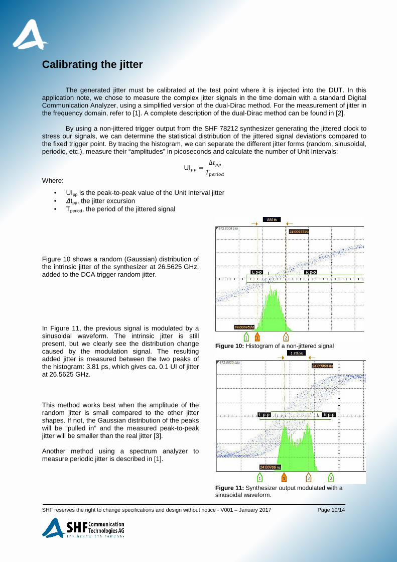
Calibrating the jitter
The generated jitter must be calibrated at the test point where it is injected into the DUT. In this
application note, we chose to measure the complex jitter signals in the time domain with a standard Digital Communication Analyzer, using a simplified version of the dual-Dirac method. For the measurement of jitter in the frequency domain, refer to [1]. A complete description of the dual-Dirac method can be found in [2].
By using a non-jittered trigger output from the SHF 78212 synthesizer generating the jittered clock to
stress our signals, we can determine the statistical distribution of the jittered signal deviations compared to the fixed trigger point. By tracing the histogram, we can separate the different jitter forms (random, sinusoidal, periodic, etc.), measure their “amplitudes” in picoseconds and calculate the number of Unit Intervals:
UI =∆
Where:
• UIpp is the peak-to-peak value of the Unit Interval jitter • ∆tpp, the jitter excursion • Tperiod, the period of the jittered signal
Figure 10 shows a random (Gaussian) distribution of the intrinsic jitter of the synthesizer at 26.5625 GHz, added to the DCA trigger random jitter. In Figure 11, the previous signal is modulated by a sinusoidal waveform. The intrinsic jitter is still present, but we clearly see the distribution change caused by the modulation signal. The resulting added jitter is measured between the two peaks of the histogram: 3.81 ps, which gives ca. 0.1 UI of jitter at 26.5625 GHz. This method works best when the amplitude of the random jitter is small compared to the other jitter shapes. If not, the Gaussian distribution of the peaks will be “pulled in” and the measured peak-to-peak jitter will be smaller than the real jitter [3]. Another method using a spectrum analyzer to measure periodic jitter is described in [1].
Figure 10: Histogram of a non-jittered signal
Figure 11: Synthesizer output modulated with a
sinusoidal waveform.
SHF reserves the right to change specifications and design without notice - V001 – January 2017 Page 11/14
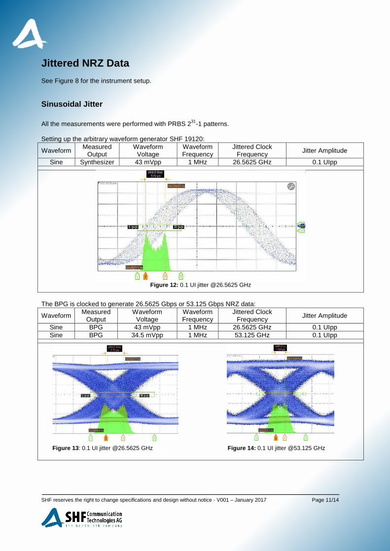
Jittered NRZ Data
See Figure 8 for the instrument setup. Sinusoidal Jitter
All the measurements were performed with PRBS 231-1 patterns. Setting up the arbitrary waveform generator SHF 19120:
Waveform Measured
Output Waveform
Voltage Waveform Frequency
Jittered Clock Frequency Jitter Amplitude
Sine Synthesizer 43 mVpp 1 MHz 26.5625 GHz 0.1 UIpp
Figure 12: 0.1 UI jitter @26.5625 GHz
The BPG is clocked to generate 26.5625 Gbps or 53.125 Gbps NRZ data:
Waveform Measured
Output Waveform
Voltage Waveform Frequency
Jittered Clock Frequency
Jitter Amplitude
Sine BPG 43 mVpp 1 MHz 26.5625 GHz 0.1 UIpp Sine BPG 34.5 mVpp 1 MHz 53.125 GHz 0.1 UIpp
Figure 13: 0.1 UI jitter @26.5625 GHz Figure 14: 0.1 UI jitter @53.125 GHz

SHF reserves the right to change specifications and design without notice - V001 – January 2017 Page 12/14
Random Jitter
The following table shows three screenshots of an NRZ signal from a BPG output jittered by a noise signal with a random Gaussian, Laplace and Uniform distribution. For each setting, the jitter measurement was done by the DCA. The Crest factor (peak amplitude divided by the RMS value of the noise distribution) was calculated from the jitter histogram.
Waveform Measured
Output Waveform
Voltage Waveform Frequency
Jittered Clock Frequency
Jitter Amplitude
Noise BPG 86 mVpp 1 MHz 26.5625 GHz 0.2 UIpp
Figure 15: NRZ with Gaussian Jitter Crest Factor = 11.5 dB
Figure 16: NRZ with Laplace Jitter Crest Factor = 15.1 dB
Figure 17: NRZ Jitter with Uniform Jitter Crest Factor = 9.3 dB
Complex Jitter: SJ + RJ
Waveform Measured
Output Waveform
Voltage Waveform Frequency
Jittered Clock Frequency
Jitter Amplitude
SJ + RJ BPG 112 mV SJ
+ 86 mV RJ
1 MHz 26.5625 GHz SJ=0.26 UIpp RJ=0.2 UIpp
Figure 18: NRZ with Sinusoidal Jitter
Figure 20: NRZ with Sinusoidal and Random
Jitter
SJ
Figure 19: SJ signal generated by the AWG
RJ
Figure 21: SJ+RJ signal generated by the AWG
SHF reserves the right to change specifications and design without notice - V001 – January 2017 Page 13/14
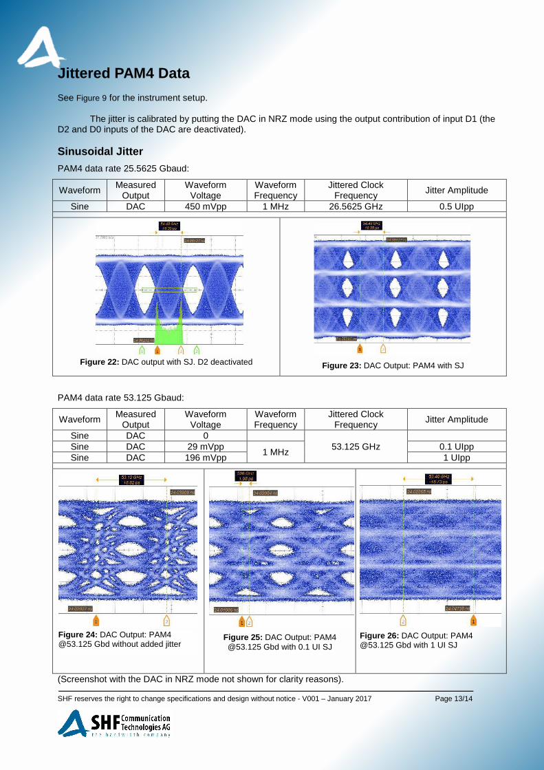
Jittered PAM4 Data
See Figure 9 for the instrument setup.
The jitter is calibrated by putting the DAC in NRZ mode using the output contribution of input D1 (the D2 and D0 inputs of the DAC are deactivated). Sinusoidal Jitter
PAM4 data rate 25.5625 Gbaud:
Waveform Measured
Output Waveform
Voltage Waveform Frequency
Jittered Clock Frequency
Jitter Amplitude
Sine DAC 450 mVpp 1 MHz 26.5625 GHz 0.5 UIpp
Figure 22: DAC output with SJ. D2 deactivated
Figure 23: DAC Output: PAM4 with SJ
PAM4 data rate 53.125 Gbaud:
Waveform Measured
Output Waveform
Voltage Waveform Frequency
Jittered Clock Frequency
Jitter Amplitude
Sine DAC 0 53.125 GHz
Sine DAC 29 mVpp
1 MHz 0.1 UIpp
Sine DAC 196 mVpp 1 UIpp
Figure 25: DAC Output: PAM4 @53.125 Gbd with 0.1 UI SJ
(Screenshot with the DAC in NRZ mode not shown for clarity reasons).
Figure 24: DAC Output: PAM4 @53.125 Gbd without added jitter
Figure 26: DAC Output: PAM4 @53.125 Gbd with 1 UI SJ

SHF reserves the right to change specifications and design without notice - V001 – January 2017 Page 14/14
Summary
By modulating the SHF synthesizer with a low frequency signal generated from an Arbitrary
Waveform Generator, one can quickly and easily create jitter signals with complex properties to drive the SHF Binary Pattern Generators to emulate jittered high speed NRZ data. Adding an SHF DAC gives the possibility to generate jittered PAM4 signals, ensuring the SHF setup is ready for the increase in modulation orders and lane rates for the anticipated serial data protocols to come.
Example Configurations – Bill of Materials
Part Instrument NRZ signals PAM4 signals
SHF 19120 Standalone Arbitrary Waveform Generator 1x 1x
SHF 78120/78122/78210/78212 Clock Source with Modulation Input 1x 1x
SHF 12105/12104 Bit Pattern Generator 1x 1x
SHF 611/612/613/614/616 Digital to Analog Converter - 1x
Table 3: Breakdown of the instruments setup
References
[1] SHF Communication Technologies Application Note: ”Jitter Injection using the Multi-Channel BPG SHF 12103/12104”. 2014.
[2] Ransom Stephens: “What the Dual-Dirac Model is and What it is Not”, October, 2006, http://ransomsnotes.com/notes.htm
[3] Teledyne Lecroy: “Understanding Jitter Calculations: Why Dj Can Be Less Than DDj (or Pj)”. 2014.