Embed Size (px)
Citation preview
CS-IIB Integrated Inverter
Technical Brief
February 2008 Manual Release 2.7 Card Revision 1.2
Copyright © 2002-2005
Creative Power Technologies P.O. Box 714 MULGRAVE Victoria, 3170 Tel: +61-3-9543-8805 Fax: +61-3-9543-8802 Email: [email protected]
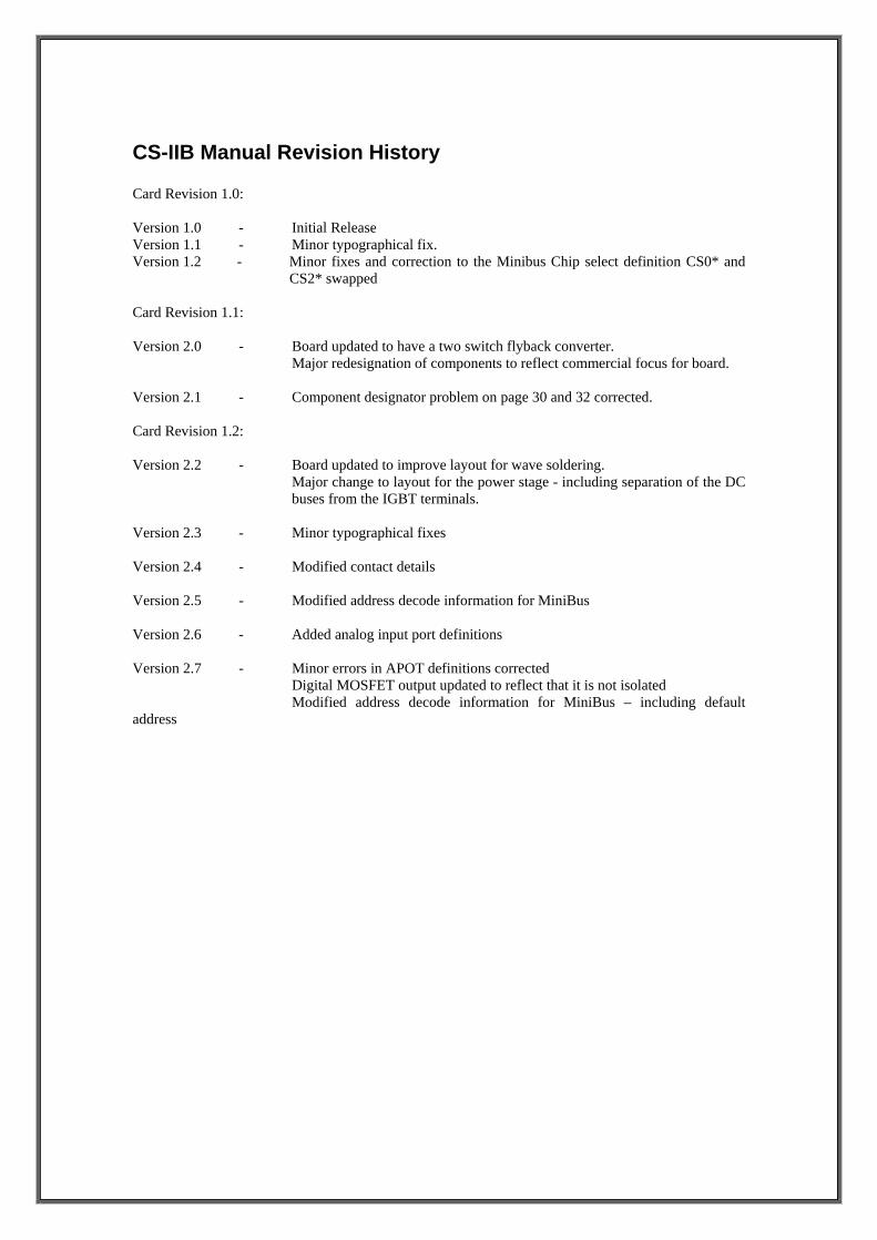
CS-IIB Manual Revision History Card Revision 1.0: Version 1.0 - Initial Release Version 1.1 - Minor typographical fix. Version 1.2 - Minor fixes and correction to the Minibus Chip select definition CS0* and
CS2* swapped Card Revision 1.1: Version 2.0 - Board updated to have a two switch flyback converter.
Major redesignation of components to reflect commercial focus for board. Version 2.1 - Component designator problem on page 30 and 32 corrected. Card Revision 1.2: Version 2.2 - Board updated to improve layout for wave soldering.
Major change to layout for the power stage - including separation of the DC buses from the IGBT terminals.
Version 2.3 - Minor typographical fixes Version 2.4 - Modified contact details Version 2.5 - Modified address decode information for MiniBus Version 2.6 - Added analog input port definitions Version 2.7 - Minor errors in APOT definitions corrected Digital MOSFET output updated to reflect that it is not isolated Modified address decode information for MiniBus – including default address
CS-IIB INTEGRATED INVERTER TECHNICAL BRIEF
© Creative Power Technologies i RELEASE 2.7 7/02/2008
Table of Contents 1.0 Overview of the CS-IIB Inverter System ........................................................................................................1
1.1 Digital I/O ............................................................................................................................................3 1.2 Analog Inputs .......................................................................................................................................3 1.3 Gate Drive Interface .............................................................................................................................4 1.4 Communications...................................................................................................................................4 1.5 On-card memory ..................................................................................................................................4 1.6 Position Encoder ..................................................................................................................................4 1.7 Keyboard Interface ...............................................................................................................................4 1.8 LCD Interface.......................................................................................................................................5 1.9 Off-card Relay Drive............................................................................................................................5 1.10 Power Stage..........................................................................................................................................5 1.11 Power Supply .......................................................................................................................................5
2.0 The MINI MICRO Concept ............................................................................................................................6 3.0 Specifications ..................................................................................................................................................7
3.1 Analog Inputs .......................................................................................................................................7 3.1.1 AC Current Inputs ................................................................................................................. 7 3.1.2 AC Voltage Inputs................................................................................................................. 7 3.1.3 DC Voltage Input .................................................................................................................. 8 3.1.4 Potentiometer Analog Inputs................................................................................................. 8
3.2 Mini Bus Interface................................................................................................................................8 3.3 Digital Inputs........................................................................................................................................8
3.3.1 TTL Level Inputs .................................................................................................................. 8 3.3.2 Position Encoder Digital Inputs ............................................................................................ 9 3.3.3 Keypad Input......................................................................................................................... 9
3.4 Digital Outputs .....................................................................................................................................9 3.4.1 TTL Level Outputs................................................................................................................ 9 3.4.2 MOSFET Output ................................................................................................................. 10 3.4.3 LCD Display Interface ........................................................................................................ 10
3.5 PWM Gate Drive Interface.................................................................................................................10 3.5.1 Isolated Gate Drives ............................................................................................................ 10 3.5.2 TTL-Level Gate Drive Output ............................................................................................ 11
3.6 Power Stage (when loaded) ................................................................................................................11 3.6.1 AC - Input ........................................................................................................................... 11 3.6.2 AC - Output......................................................................................................................... 11 3.6.3 Additional DC Bus .............................................................................................................. 11
3.7 Communications Interface .................................................................................................................12 3.7.1 RS-232 Interface ................................................................................................................. 12 3.7.2 High Speed Serial Peripheral Interface ............................................................................... 12
3.8 General ...............................................................................................................................................12 3.9 Power Supply .....................................................................................................................................12
Appendix A Component Layout ....................................................................................................................14 Appendix B Mechanical Layout – including Test Points and Links ..............................................................16
CS-IIB INTEGRATED INVERTER TECHNICAL BRIEF
© Creative Power Technologies 1 RELEASE 2.7 7/02/2008
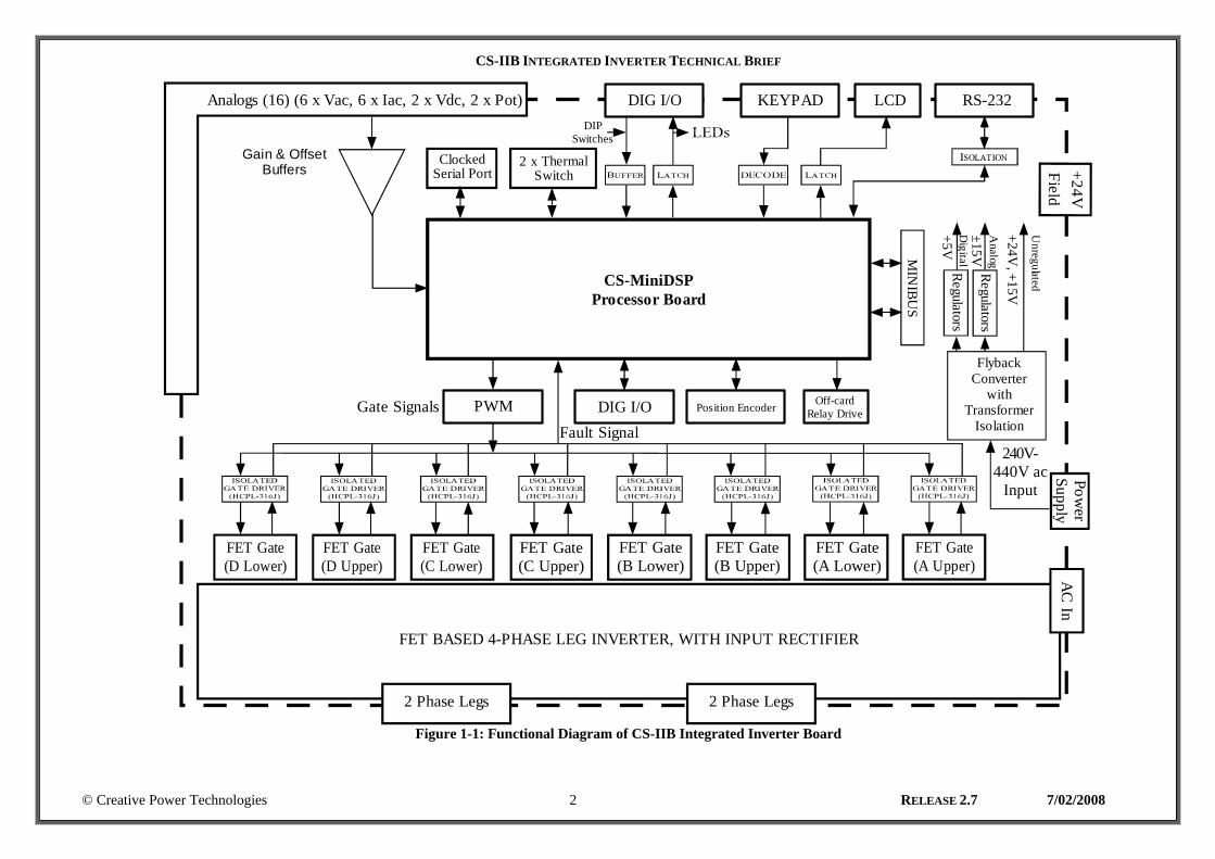
1.0 Overview of the CS-IIB Inverter System The CS-IIB is a flexible, low voltage, 4-phase leg integrated inverter system that has been designed for applications requiring a single simple inverter platform. The board includes an on-card FET/IGBT based power stage and sufficient digital and analog conditioned signals to enable it to operate, with plug-in CS-MiniDSP processor card, as a standalone voltage source inverter without additional circuitry. The board consists of 6 major sections: • 8 off complementary isolated gate driver PWM outputs, with common fault interrupt • 4 phase leg TO-247 FET/IGBT based power stage, with associated input rectifier. • Isolated RS-232 serial interface • 16 off conditioned analog inputs • LCD interface / Keypad interface / Digital I/O • Switch-mode power supply to generate all on-card supplies The power stage of the CS-IIB is capable of operation up to 15A at up to a 400V DC bus, and is designed for TO-247 FET/IGBT based switching devices. Sufficient flexibility has been designed in to the power stage to permit operation in any of the following configurations: • Single bus, Dual-H Bridge inverter (back-to-back DC converter operation) • Dual bus, Dual-H Bridge inverter • Single bus 3 leg inverter • Dual bus 3 leg inverter with single leg buck 1 • Single bus 4 leg inverter Alternatively, the system can be operated without the power stage, with the gate drivers supplying a larger capacity (up to 30kVA) and higher voltage (600Vdc) inverter. For even larger external power stage devices, the gate driver output capacity can be increased to 8Apeak using a transistor totem pole pair on the driver output. The CS-IIB Integrated Inverter measures 345mm x 285mm.
On-card facilities include:
• Serial Interface (Isolated RS232) • Quadrature Position Encoder input with Index • High speed clocked serial peripheral interface • 4096 bit serial ROM • Dual Temperature Sensors (digital) • Multiple off-card digital I/O ports • On-card DIP switches and status LEDs • 6 off AC current inputs • 6 off differential AC voltage inputs • 2 off differential DC voltage inputs • 2 off potentiometer analog inputs • 1 off 4x5-way keypad decoder • LCD interface, with contrast • 1 off MOSFET switch output • On-card soft start relay with associated circuitry • 8 off complementary isolated gate driver PWM outputs, with common fault interrupt • 8 bit MINI bus interface (INTEL iSBX compatible), • +24V isolated field supply Figure 1-1 shows a functional block diagram of the CS-IIB Integrated Inverter, illustrating all major sections.
1 Requires external inductors
CS-IIB INTEGRATED INVERTER TECHNICAL BRIEF
© Creative Power Technologies 2 RELEASE 2.7 7/02/2008
+5VD
igitalRegulators
Analog
Regulators±15V
Unregulated
+24V, +15V
FlybackConverter
withTransformer
Isolation
CS-MiniDSPProcessor Board
FET Gate(D Upper)
Fault SignalGate Signals
FET Gate(C Lower)
FET Gate(C Upper)
FET Gate(B Lower)
FET Gate(B Upper)
FET Gate(A Lower)
FET Gate(D Lower)
FET Gate(A Upper)
Gain & OffsetBuffers
RS-232
Power
Supply
240V-440V ac
Input
+24VField
ClockedSerial Port
LCDKEYPADDIG I/O
Position EncoderDIG I/O
FET BASED 4-PHASE LEG INVERTER, WITH INPUT RECTIFIER
2 Phase Legs 2 Phase Legs
AC
In
Analogs (16) (6 x Vac, 6 x Iac, 2 x Vdc, 2 x Pot)
2 x ThermalSwitch
MIN
IBUS
DIPSwitches
PWM Off-cardRelay Drive
Figure 1-1: Functional Diagram of CS-IIB Integrated Inverter Board
CS-IIB INTEGRATED INVERTER TECHNICAL BRIEF
© Creative Power Technologies 3 RELEASE 2.7 7/02/2008
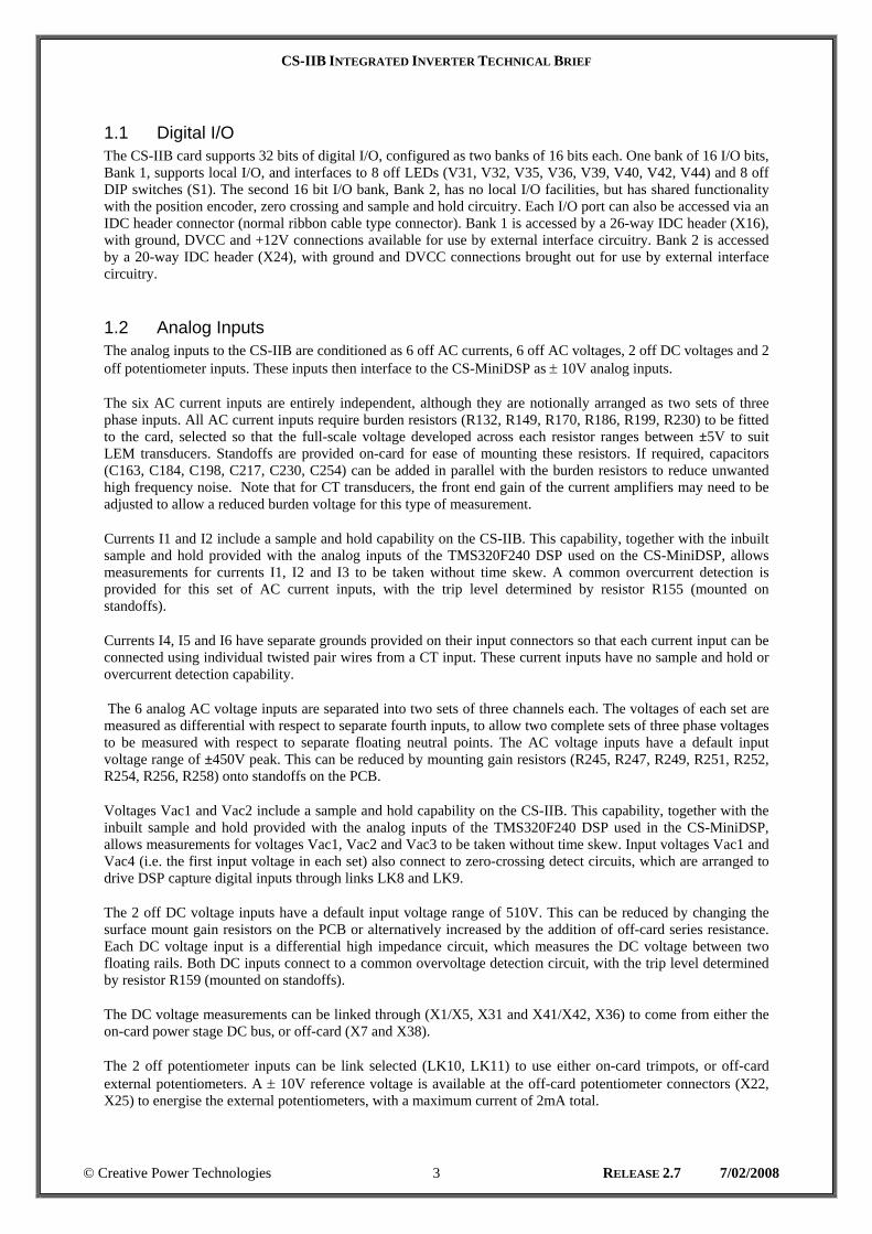
1.1 Digital I/O The CS-IIB card supports 32 bits of digital I/O, configured as two banks of 16 bits each. One bank of 16 I/O bits, Bank 1, supports local I/O, and interfaces to 8 off LEDs (V31, V32, V35, V36, V39, V40, V42, V44) and 8 off DIP switches (S1). The second 16 bit I/O bank, Bank 2, has no local I/O facilities, but has shared functionality with the position encoder, zero crossing and sample and hold circuitry. Each I/O port can also be accessed via an IDC header connector (normal ribbon cable type connector). Bank 1 is accessed by a 26-way IDC header (X16), with ground, DVCC and +12V connections available for use by external interface circuitry. Bank 2 is accessed by a 20-way IDC header (X24), with ground and DVCC connections brought out for use by external interface circuitry.
1.2 Analog Inputs The analog inputs to the CS-IIB are conditioned as 6 off AC currents, 6 off AC voltages, 2 off DC voltages and 2 off potentiometer inputs. These inputs then interface to the CS-MiniDSP as ± 10V analog inputs.
The six AC current inputs are entirely independent, although they are notionally arranged as two sets of three phase inputs. All AC current inputs require burden resistors (R132, R149, R170, R186, R199, R230) to be fitted to the card, selected so that the full-scale voltage developed across each resistor ranges between ±5V to suit LEM transducers. Standoffs are provided on-card for ease of mounting these resistors. If required, capacitors (C163, C184, C198, C217, C230, C254) can be added in parallel with the burden resistors to reduce unwanted high frequency noise. Note that for CT transducers, the front end gain of the current amplifiers may need to be adjusted to allow a reduced burden voltage for this type of measurement.
Currents I1 and I2 include a sample and hold capability on the CS-IIB. This capability, together with the inbuilt sample and hold provided with the analog inputs of the TMS320F240 DSP used on the CS-MiniDSP, allows measurements for currents I1, I2 and I3 to be taken without time skew. A common overcurrent detection is provided for this set of AC current inputs, with the trip level determined by resistor R155 (mounted on standoffs).
Currents I4, I5 and I6 have separate grounds provided on their input connectors so that each current input can be connected using individual twisted pair wires from a CT input. These current inputs have no sample and hold or overcurrent detection capability.
The 6 analog AC voltage inputs are separated into two sets of three channels each. The voltages of each set are measured as differential with respect to separate fourth inputs, to allow two complete sets of three phase voltages to be measured with respect to separate floating neutral points. The AC voltage inputs have a default input voltage range of ±450V peak. This can be reduced by mounting gain resistors (R245, R247, R249, R251, R252, R254, R256, R258) onto standoffs on the PCB.
Voltages Vac1 and Vac2 include a sample and hold capability on the CS-IIB. This capability, together with the inbuilt sample and hold provided with the analog inputs of the TMS320F240 DSP used in the CS-MiniDSP, allows measurements for voltages Vac1, Vac2 and Vac3 to be taken without time skew. Input voltages Vac1 and Vac4 (i.e. the first input voltage in each set) also connect to zero-crossing detect circuits, which are arranged to drive DSP capture digital inputs through links LK8 and LK9.
The 2 off DC voltage inputs have a default input voltage range of 510V. This can be reduced by changing the surface mount gain resistors on the PCB or alternatively increased by the addition of off-card series resistance. Each DC voltage input is a differential high impedance circuit, which measures the DC voltage between two floating rails. Both DC inputs connect to a common overvoltage detection circuit, with the trip level determined by resistor R159 (mounted on standoffs).
The DC voltage measurements can be linked through (X1/X5, X31 and X41/X42, X36) to come from either the on-card power stage DC bus, or off-card (X7 and X38).
The 2 off potentiometer inputs can be link selected (LK10, LK11) to use either on-card trimpots, or off-card external potentiometers. A ± 10V reference voltage is available at the off-card potentiometer connectors (X22, X25) to energise the external potentiometers, with a maximum current of 2mA total.
CS-IIB INTEGRATED INVERTER TECHNICAL BRIEF
© Creative Power Technologies 4 RELEASE 2.7 7/02/2008
1.3 Gate Drive Interface The CS-IIB supports 8 PWM channel outputs generated by the plug-in CS-MiniDSP TMS320F240 processor board (or equivalent), and converts these outputs to 8 isolated gate driver outputs through HCPL-316J gate driver chips. Isolated supplies are generated on-card for each gate drive circuit.
Gate fault signals from the eight HCPL-316J gate driver chips are linked together and connected to the PDPINT* interrupt (X17). This interrupt provides a hardware interrupt to the CS-MiniDSP immediately on detection of a fault, which disables the PWM signals using internal hardware logic within the DSP.
If the power stage is not loaded on-card, the TO-247 mounting holes can be loaded with terminal block headers to enable the gate drive signals to interface off-card modules. If a gate drive current greater than 2A is required (the HCPL-316J is capable of a maximum of 2A output), a totem pole option can be added to each gate drive circuit to drive larger off-card switching devices (up to 8A peak).
A 20-way IDC header (X29) is also provided to enable the logic level gate signals to be connected to an alternative source or output. To drive the gate signals from an off-card source (ie not through the CS-MiniDSP) the plug-in CS-MiniDSP must have U11 removed. This is the 74HC245 driver buffer, which connects the PWM signals from the CS-MiniDSP to the CS-IIB card.
1.4 Communications The CS-IIB integrated inverter board supports an isolated RS-232 serial interface, and a non-isolated TTL high-speed synchronous serial peripheral interface.
The RS-232 serial port connects to the CS-MiniDSP UART through X14, and is isolated through HCPL-2211 high-speed optocouplers. An NMF0505 DC-DC converter provides the isolated supply for this serial port.
The TTL high-speed synchronous serial peripheral interface can be used to communicate to other computer systems, and connects to the CS-MiniDSP through X20. The interface is buffered to support either master or slave protocol, selected by software.
1.5 On-card memory The CS-IIB integrated inverter board has no direct on-card memory, as it is designed to have a processor board plug-in to the pin strip headers provided. The preferred controller board is the CS-MiniDSP, which supports 64k x 16 bits each of on-card Program RAM and Data RAM.
The CS-IIB integrated inverter board does support 256 x 16 bits of non-volatile serial ROM. This ROM is accessed using the high-speed serial port pins through connector X20.
1.6 Position Encoder The position encoder interface accepts quadrature encoded pulses from a relative position encoder system, and uses these pulses to update a 16 or 32 bit position counter (as selected by software) within the DSP. The phase A and Phase B signals interface to the CS-MiniDSP using shared digital I/O bits through connector X23.
A separate index pulse input can be used to generate an interrupt to reset this counter for initialisation purposes. This signal interfaces to the CS-MiniDSP through connector X17.
The encoder input signals are at 5V TTL levels, diode clamped to avoid damage caused by input overvoltages. A +12V supply is also provided at the encoder input connector (X18) for use by the external encoder circuitry.
1.7 Keyboard Interface The keypad input is arranged to accept a 9 wire, 4x5 matrix keypad input, which interfaces to a 74C923 keypad decoder. This encoder is accessed as a Mini Bus peripheral port by the CS-MiniDSP controller.
CS-IIB INTEGRATED INVERTER TECHNICAL BRIEF
© Creative Power Technologies 5 RELEASE 2.7 7/02/2008
1.8 LCD Interface The LCD interface is arranged to directly suit all 1 and 2 line Handok or Optrex character type LCD display modules. The interface connects to the LCD display through a 16 way IDC header connector (X8). The interface signals are an 8 bit latched data byte, and four latched control bits which are toggled by the CS-MiniDSP to generate the LCD display control signals. All interface signals are TTL.
The LCD interface also provides a –12V adjustable contrast supply, and a +5V LED backlight supply controlled by a transistor switch.
The LCD interface data and control bit latches are accessed as Mini Bus peripheral ports by the CS-MiniDSP controller.
1.9 Off-card Relay Drive The off-card relay is a switched +12V 1A supply controlled by a Power FET from a latched digital output bit on the CS-IIB card. The digital bit is accessed as a data bit on a Mini Bus peripheral port by the CS-MiniDSP controller.
1.10 Power Stage The CS-IIB has a four phase leg TO-247 based power stage that is designed primarily for TO-247 FET/IGBT switching devices. The power stage consists of a single-phase input rectifier with soft-start relay, DC bus capacitors and 8 off TO-218 / TO-247 / TO-264 FET or IGBT devices. A single T-shaped heatsink is used to mount all discrete semiconductor devices. The power stage has been designed to operate at up to 400V and a 12A load current in any of the following configurations:
• Single bus, Dual-H Bridge inverter (back-to-back DC converter operation) • Dual bus, Dual-H Bridge inverter • Single bus 3 leg inverter • Dual bus 3 leg inverter with single leg buck 2 • Single bus 4 leg inverter
1.11 Power Supply The standard CS-IIB integrated inverter board has an on-card switch mode power supply that accepts an input voltage in the range of 90V – 270V AC or 130V – 370V DC. The SMPS generates all necessary on-card supplies as well as an isolated +24V field supply for off-card use.
2 Requires external inductors
CS-IIB INTEGRATED INVERTER TECHNICAL BRIEF
© Creative Power Technologies 6 RELEASE 2.7 7/02/2008
2.0 The MINI MICRO Concept The MINI MICRO concept was originally developed as a low-cost alternative for developing microprocessor-based industrial controllers. In essence, the concept is an open-ended standard BUS equivalent set of microprocessor cards, which do not incur the usual cost overheads of back planes and card cages. In contrast to fully custom-designed systems, the central microprocessor card will always ‘startup’, and flexible software support tools are available off-the-shelf. However, unlike BUS based systems, standard MINI cards are relatively low cost, and custom designs can be readily prototyped and incorporated into a system.
All MINI MICRO peripheral cards are small, nominally measuring only 12.7cm by 5.6cm. Each card has three mounting holes, allowing cards to be stacked one on top of the other using head-to-tail mounting supports. A 36-way ribbon cable interconnects between the cards, supporting an 8 bit I/O MINI BUS (similar to the INTEL iSBX microbus). The MINI BUS has address space for up to 24 I/O ports. All standard MINI BUS peripheral cards require only 2 ports to interface to the processor card, allowing for a maximum of 12 I/O cards to be stacked together in any one system.
There are two main processor cards available in the MINI MICRO system, one using a CS-64180 processor and the other using a TMS320F240 DSP. The CS-64180 processor supports up to 64k EPROM, 96k RAM, 2 serial ports, on-card memory management, on-card power supplies and of course the MINI BUS. The TMS320F240 DSP version enables additional features to be made available on a somewhat larger base board. The DSP chip supports 64k x 16bit EPROM, 128k x 16bit RAM, 1 serial port, 8 PWM outputs, 16 analog inputs (10 bits), 16 digital I/O channels, external interrupts, a serial port, a clocked serial port, a JTAG port, on-card memory management, on-card power supplies and of course the MINI BUS. Other standard MINI cards provide digital input/outputs (TTL levels), isolated digital I/O (AC/DC, relays, MOSFETs, Triacs), analog input/output (8 bit and 12 bit), dial-up modems, real time-of-day clock, and ‘wake up’ data logging.
The use of ribbon cable as the interconnecting bus offers considerable flexibility to the system, since it allows cards not only to be stacked together, but also to be mounted to suit an individual system’s needs. For example, a keyboard/display card could be mounted on a front panel, and connected to the main MINI MICRO stack by extending and twisting the 36-way MINI BUS ribbon cable. Furthermore, the lack of a card cage means that physically non-standard I/O cards can be accommodated, and even mounted in the card stack if the spacing of the three mounting holes is maintained.
Standard MINI MICRO cards are all CMOS based, supporting the low power concept. The CS-64180 processor card, for example, only requires 50mA of current and the CS-MiniDSP requires 85mA. Where an I/O card must support significant external load (digital I/O perhaps), alternative power supply connections are provided on the I/O card. Furthermore, MINI MICRO cards are specifically designed for industrial applications, and hence factors such as battery-backup of RAM memory, interference free power supplies, etc are designed into the main processor card.
CS-IIB INTEGRATED INVERTER TECHNICAL BRIEF
© Creative Power Technologies 7 RELEASE 2.7 7/02/2008
3.0 Specifications
3.1 Analog Inputs Number of Channels 16
Plug-In Interface to header X34 (which corresponds to J4 on the CS-MiniDSP)
3.1.1 AC Current Inputs
Definition
3 off twisted pair 3-wire connections and 3 off twisted pair 4-wire connections providing conditioned AC current inputs compatible with CT’s and LEM’s. Burden resistors (R132, R149, R170, R186, R199, R230) and low pass filter capacitors (C163, C184, C198, C217, C230, C254) are required to suit input current requirements
Input Voltage Range ±5V maximum peak (set by burden resistor for required current)
Burden Resistor AXIAL0.4 component mounted on-card and sized according to input voltage range and maximum required current input AC current input impedance is 5k0 without the burden resistor
Overcurrent Protection Overcurrent linkable interrupt to PDPINT* (LK4) for first three current inputs I1, I2 and I3. Trigger current determined by resistor selection (R155)
Sample and Hold Sample and Hold circuitry fitted for currents I1 and I2. S&H control signal supplied from CS-MiniDSP as digital output bit R4*, I/O Bank 2 (X23) through link LK12
LEM Supply ± 15V 100mA supply available to support LEMs. (X26, X30, X32, X33, X35, X37)
Dynamic Response Cut-off frequency >150kHz
PCB Connections
3 off 3 terminal plug-in PCB Mounting Terminal Block with ±15V. (X33, X35, X37)
3 off 4 terminal plug-in PCB Mounting Terminal Block with ±15V and AGND. (X26, X30, X32)
3.1.2 AC Voltage Inputs Definition 6 off AC voltage differential analog inputs, arranged as two sets of 3 inputs. Each
set measures voltage with respect to a separate fourth floating common
Input Voltage Range
±450 Vac maximum peak Lower range available with placement of scaling resistors (R245, R247, R249, R251, R252, R254, R256, R258)
Higher range available through placement of off-card series resistors
Sample and Hold Sample and Hold circuitry fitted for voltages Vac1 and Vac2. S&H control signal supplied from CS-MiniDSP as digital output bit R4*, I/O Bank 2 (X23) through link LK12
Input Protection High input impedance, 450kΩ in default configuration
Dynamic Response Cut-off frequency > 450kHz
PCB Connections 7 pin plug-in PCB Mounting Terminal Block (X39, X40)
CS-IIB INTEGRATED INVERTER TECHNICAL BRIEF
© Creative Power Technologies 8 RELEASE 2.7 7/02/2008
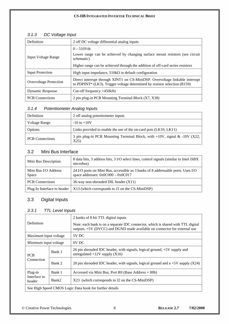
3.1.3 DC Voltage Input Definition 2 off DC voltage differential analog inputs
Input Voltage Range
0 – 510Vdc Lower range can be achieved by changing surface mount resistors (see circuit schematic)
Higher range can be achieved through the addition of off-card series resistors
Input Protection High input impedance, 510kΩ in default configuration
Overvoltage Protection Direct interrupt through XINT1 on CS-MiniDSP. Overvoltage linkable interrupt to PDPINT* (LK3). Trigger voltage determined by resistor selection (R159)
Dynamic Response Cut-off frequency >450kHz
PCB Connections 2 pin plug-in PCB Mounting Terminal Block (X7, X38)
3.1.4 Potentiometer Analog Inputs Definition 2 off analog potentiometer inputs
Voltage Range -10 to +10V
Options Links provided to enable the use of the on-card pots (LK10, LK11)
PCB Connections 3 pin plug-in PCB Mounting Terminal Block, with +10V, signal & -10V (X22, X25)
3.2 Mini Bus Interface
Mini Bus Description 8 data bits, 3 address bits, 3 I/O select lines, control signals (similar to Intel iSBX microbus)
Mini Bus I/O Address Space
24 I/O ports on Mini Bus, accessible as 3 banks of 8 addressable ports. Uses I/O space addresses: 0x0C000 – 0x0C017
PCB Connections 36-way non-shrouded DIL header (X11)
Plug-In Interface to header X13 (which corresponds to J1 on the CS-MiniDSP)
3.3 Digital Inputs
3.3.1 TTL Level Inputs
Definition 2 banks of 8 bit TTL digital inputs
Note: each bank is on a separate IDC connector, which is shared with TTL digital outputs. +5V (DVCC) and DGND made available on connector for external use
Maximum input voltage 5V DC
Minimum input voltage 0V DC
Bank 1 26 pin shrouded IDC header, with signals, logical ground, +5V supply and unregulated +12V supply (X16) PCB
Connection Bank 2 20 pin shrouded IDC header, with signals, logical ground and a +5V supply (X24)
Bank 1 Accessed via Mini Bus, Port R0 (Base Address + 00h) Plug-in Interface to header Bank2 X23 (which corresponds to J2 on the CS-MiniDSP)
See High Speed CMOS Logic Data book for further details
CS-IIB INTEGRATED INVERTER TECHNICAL BRIEF
© Creative Power Technologies 9 RELEASE 2.7 7/02/2008
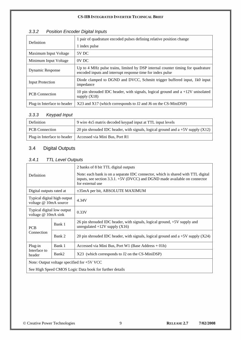
3.3.2 Position Encoder Digital Inputs
Definition 1 pair of quadrature encoded pulses defining relative position change
1 index pulse
Maximum Input Voltage 5V DC
Minimum Input Voltage 0V DC
Dynamic Response Up to 4 MHz pulse trains, limited by DSP internal counter timing for quadrature encoded inputs and interrupt response time for index pulse
Input Protection Diode clamped to DGND and DVCC, Schmitt trigger buffered input, 1k0 input impedance
PCB Connection 10 pin shrouded IDC header, with signals, logical ground and a +12V unisolated supply (X18)
Plug-in Interface to header X23 and X17 (which corresponds to J2 and J6 on the CS-MiniDSP)
3.3.3 Keypad Input Definition 9 wire 4x5 matrix decoded keypad input at TTL input levels
PCB Connection 20 pin shrouded IDC header, with signals, logical ground and a +5V supply (X12)
Plug-in Interface to header Accessed via Mini Bus, Port R1
3.4 Digital Outputs
3.4.1 TTL Level Outputs
Definition
2 banks of 8 bit TTL digital outputs
Note: each bank is on a separate IDC connector, which is shared with TTL digital inputs, see section 3.3.1. +5V (DVCC) and DGND made available on connector for external use
Digital outputs rated at ±35mA per bit, ABSOLUTE MAXIMUM
Typical digital high output voltage @ 10mA source 4.34V
Typical digital low output voltage @ 10mA sink 0.33V
Bank 1 26 pin shrouded IDC header, with signals, logical ground, +5V supply and unregulated +12V supply (X16) PCB
Connection Bank 2 20 pin shrouded IDC header, with signals, logical ground and a +5V supply (X24)
Bank 1 Accessed via Mini Bus, Port W1 (Base Address + 01h) Plug-in Interface to header Bank2 X23 (which corresponds to J2 on the CS-MiniDSP)
Note: Output voltage specified for +5V VCC
See High Speed CMOS Logic Data book for further details
CS-IIB INTEGRATED INVERTER TECHNICAL BRIEF
© Creative Power Technologies 10 RELEASE 2.7 7/02/2008
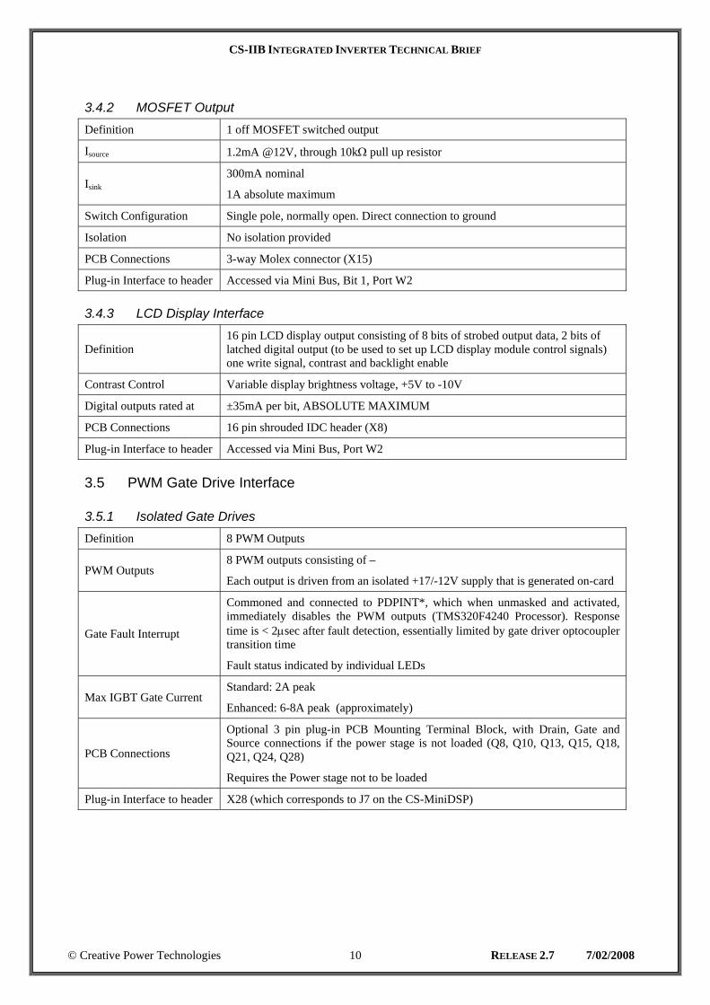
3.4.2 MOSFET Output Definition 1 off MOSFET switched output
Isource 1.2mA @12V, through 10kΩ pull up resistor
Isink 300mA nominal
1A absolute maximum
Switch Configuration Single pole, normally open. Direct connection to ground
Isolation No isolation provided
PCB Connections 3-way Molex connector (X15)
Plug-in Interface to header Accessed via Mini Bus, Bit 1, Port W2
3.4.3 LCD Display Interface
Definition 16 pin LCD display output consisting of 8 bits of strobed output data, 2 bits of latched digital output (to be used to set up LCD display module control signals) one write signal, contrast and backlight enable
Contrast Control Variable display brightness voltage, +5V to -10V
Digital outputs rated at ±35mA per bit, ABSOLUTE MAXIMUM
PCB Connections 16 pin shrouded IDC header (X8)
Plug-in Interface to header Accessed via Mini Bus, Port W2
3.5 PWM Gate Drive Interface
3.5.1 Isolated Gate Drives Definition 8 PWM Outputs
PWM Outputs 8 PWM outputs consisting of –
Each output is driven from an isolated +17/-12V supply that is generated on-card
Gate Fault Interrupt
Commoned and connected to PDPINT*, which when unmasked and activated, immediately disables the PWM outputs (TMS320F4240 Processor). Response time is < 2μsec after fault detection, essentially limited by gate driver optocoupler transition time
Fault status indicated by individual LEDs
Max IGBT Gate Current Standard: 2A peak
Enhanced: 6-8A peak (approximately)
PCB Connections
Optional 3 pin plug-in PCB Mounting Terminal Block, with Drain, Gate and Source connections if the power stage is not loaded (Q8, Q10, Q13, Q15, Q18, Q21, Q24, Q28)
Requires the Power stage not to be loaded
Plug-in Interface to header X28 (which corresponds to J7 on the CS-MiniDSP)
CS-IIB INTEGRATED INVERTER TECHNICAL BRIEF
© Creative Power Technologies 11 RELEASE 2.7 7/02/2008
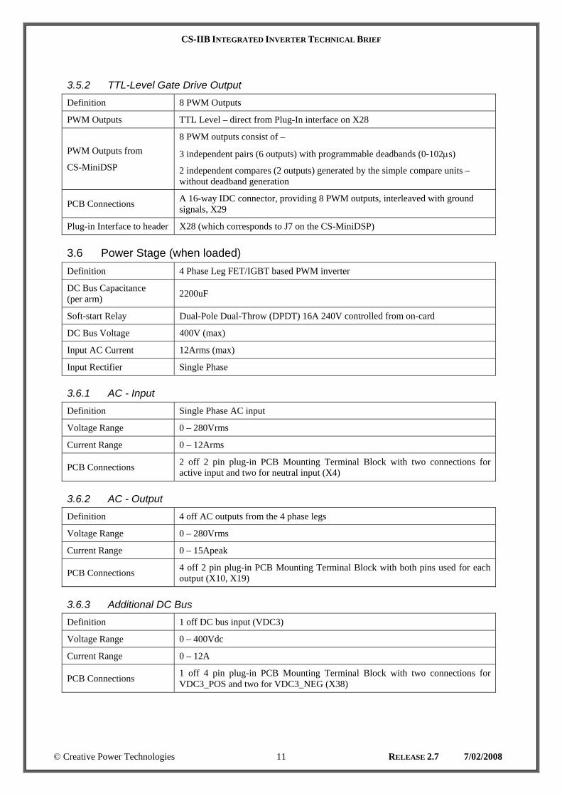
3.5.2 TTL-Level Gate Drive Output Definition 8 PWM Outputs
PWM Outputs TTL Level – direct from Plug-In interface on X28
PWM Outputs from
CS-MiniDSP
8 PWM outputs consist of –
3 independent pairs (6 outputs) with programmable deadbands (0-102μs)
2 independent compares (2 outputs) generated by the simple compare units – without deadband generation
PCB Connections A 16-way IDC connector, providing 8 PWM outputs, interleaved with ground signals, X29
Plug-in Interface to header X28 (which corresponds to J7 on the CS-MiniDSP)
3.6 Power Stage (when loaded) Definition 4 Phase Leg FET/IGBT based PWM inverter
DC Bus Capacitance (per arm) 2200uF
Soft-start Relay Dual-Pole Dual-Throw (DPDT) 16A 240V controlled from on-card
DC Bus Voltage 400V (max)
Input AC Current 12Arms (max)
Input Rectifier Single Phase
3.6.1 AC - Input Definition Single Phase AC input
Voltage Range 0 – 280Vrms
Current Range 0 – 12Arms
PCB Connections 2 off 2 pin plug-in PCB Mounting Terminal Block with two connections for active input and two for neutral input (X4)
3.6.2 AC - Output Definition 4 off AC outputs from the 4 phase legs
Voltage Range 0 – 280Vrms
Current Range 0 – 15Apeak
PCB Connections 4 off 2 pin plug-in PCB Mounting Terminal Block with both pins used for each output (X10, X19)
3.6.3 Additional DC Bus Definition 1 off DC bus input (VDC3)
Voltage Range 0 – 400Vdc
Current Range 0 – 12A
PCB Connections 1 off 4 pin plug-in PCB Mounting Terminal Block with two connections for VDC3_POS and two for VDC3_NEG (X38)
CS-IIB INTEGRATED INVERTER TECHNICAL BRIEF
© Creative Power Technologies 12 RELEASE 2.7 7/02/2008
3.7 Communications Interface
3.7.1 RS-232 Interface
Definition RS-232 connection, providing two pin serial communications for interface to a standard PC serial port
Isolation 1kV
Compatibility Links provided to enable the board to be configured as a DTE or a DCE (LK1). Default is configuration as a DCE
PCB Connections 10-way IDC connector, with pin outs to suit standard PC 9 pin serial port (X6)
Plug-in Interface to header X14 (which corresponds to J5 on the CS-MiniDSP)
3.7.2 High Speed Serial Peripheral Interface
Definition Half duplex synchronous clocked serial peripheral interface. Capable of operating in Master or Slave mode (software selected)
Compatibility Compatible with the TMS320F240 SPI module
PCB Connection 5-way Molex connector (X21)
Plug-in Interface to header X20 (which corresponds to J9 on the CS-MiniDSP)
3.8 General
L: 345mm
W: 285mm Physical Dimensions
H: 80mm approx.
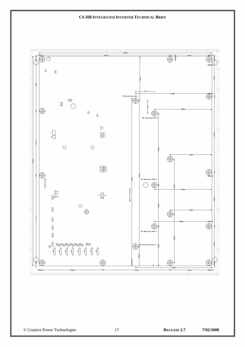
Mounting Arrangement 13 off 4.5 mm holes spaced in a grid across the PCB (see Appendix B)
Environmental 0 – 50°C ambient operating temperature
5% - 95% non condensing humidity
3.9 Power Supply
Input Voltage Range 90Vac – 270Vac (130Vdc – 370Vdc)
Standalone Input Current 80-30 mA
Max Input Power Approx. 36W
2A Slow Blow Fuse Protected
+12V Digital from which the +5V Digital is generated using a regulator
±15V for Analog circuitry
+24V Unregulated field supply - 1A total
Supplies Generated
on-card
+17V/-12V Gate Drive Supply
Input Power Connector 3 pin plug-in PCB Mounting Terminal Block: Active, Neutral, EARTH (X3)
Output Power Connectors 2 pin plug-in PCB Mounting Terminal Block: +24V, GND_24V (X2)
2 pin Molex connector: +12V, DGND (X9)
CS-IIB INTEGRATED INVERTER TECHNICAL BRIEF
© Creative Power Technologies 13 RELEASE 2.7 7/02/2008
Appendices
CS-IIB INTEGRATED INVERTER TECHNICAL BRIEF
© Creative Power Technologies 14 RELEASE 2.7 7/02/2008
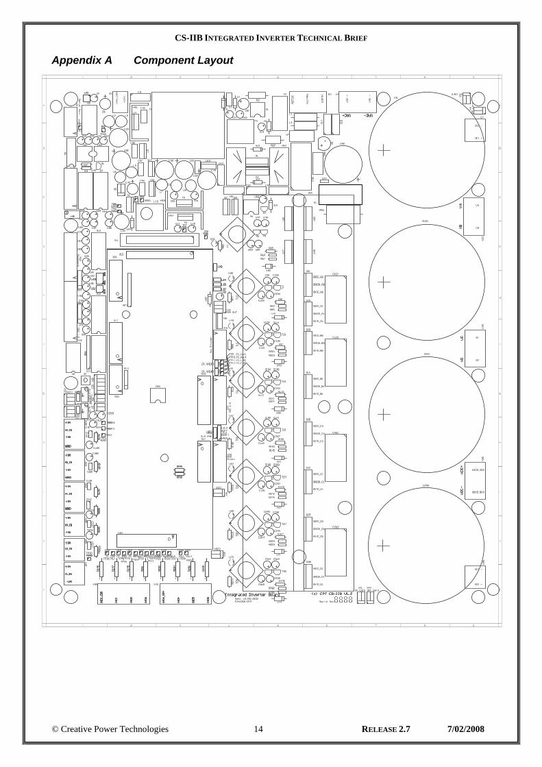
Appendix A Component Layout
CS-IIB INTEGRATED INVERTER TECHNICAL BRIEF
© Creative Power Technologies 15 RELEASE 2.7 7/02/2008
CS-IIB INTEGRATED INVERTER TECHNICAL BRIEF
© Creative Power Technologies 16 RELEASE 2.7 7/02/2008
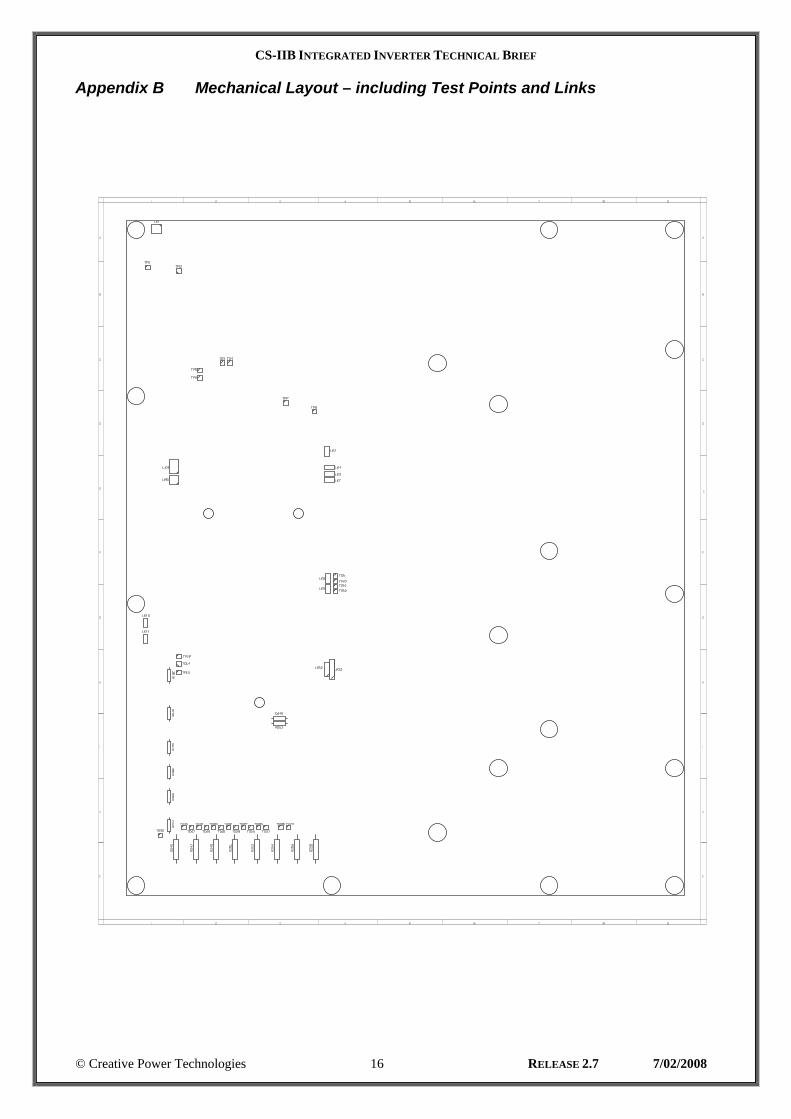
Appendix B Mechanical Layout – including Test Points and Links
CS-IIB INTEGRATED INVERTER TECHNICAL BRIEF
© Creative Power Technologies 17 RELEASE 2.7 7/02/2008


![xVision Ground Support Rigging System - [co]motion Ground Support Rigging System ... (4 tiles long x 7 tiles high) 1 Main base 2 Front Legs 2 Back Legs 2 x 1794 mm Ladders 2 x 475mm](https://img.pdfslide.net/doc/110x75/5ad5e0e27f8b9a6d708d6694/xvision-ground-support-rigging-system-co-ground-support-rigging-system-4.jpg)


![MYTH PHASE - II - [CLASS X - 08.11.2020]](https://img.pdfslide.net/doc/110x75/6198d68debe4100fa2170716/myth-phase-ii-class-x-08112020.jpg)