Embed Size (px)
Citation preview
DEPARTMENT OF ELECTRONICS AND COMMUNICATION ENGINEERING
SUBJECT CODE: CS1202
ELECTRONIC CIRCUITS AND DIGITAL SYSTEMS
(FOR THIRD SEMESTER IT & CSE)
TWO MARK QUESTIONS &ANSWERS
MaanavaN.ComMaanavaN.ComMaanavaN.ComMaanavaN.Com
CS 1202: ELECTRONIC CIRCUITS AND DIGITAL SYSTEMS
TWO MARK QUESTIONS AND ANSWERS
1. What is depletion region in PN junction?
The region around the junction from which the mobile charge carriers (electrons and
holes) are depleted is called as depletion region. Since this region has immobile ions,
which are electrically charged, the depletion region is also known as space charge region.
2. Give the other names of depletion region?
i. space charge region
ii. Transition region
3. What is barrier potential?
Because of the oppositely charged ions present on both sides of PN junction an electric
potential is established across the junction even without any external voltage source
which is termed as barrier potential.
4. What is meant by biasing a PN junction?
Connecting a PN junction to an external voltage source is biasing a PN junction.
5. What are the types of biasing a PN junction?
1. Forward bias 2. Reverse bias.
6. What is forward bias and reverse bias in a PN junction?
When positive terminal of the external supply is connected to P region and negative
terminal to N region, the PN junction is said to be forward biased. Under forward biased
condition the PN region offers a very low resistance and a large amount of current flows
through it.
7. What is reverse bias in a PN junction?
When positive terminal of the external supply is connected to N type and negative
terminal to P type then the PN junction is said to be in reverse bias. Under reverse biased
condition the PN region offers a very high resistance and a small amount of current flows
through it.
8. What is Reverse saturation current?
The current due to the minority carriers in reverse bias is said to be reverse saturation
current. This current is independent of the value of the reverse bias voltage.
MaanavaN.ComMaanavaN.ComMaanavaN.ComMaanavaN.ComMaanavaN.ComMaanavaN.ComMaanavaN.ComMaanavaN.ComMaanavaN.ComMaanavaN.Com
9. Why contact differences of potential exist in PN junction?
When a PN junction is formed by placing a p-type and n-type material in intimate
contact, the Fermi level throughout the newly formed specimen is not constant at
equilibrium. There will be transfer of electron and energy until Fermi levels in the two
sides did line up. But the valence and conduction band in p side cannot be at the at the
same level as in n side .this shift in energy level results in contact difference of potential.
10. Give the expression of contact difference of potential?
E0 = kT ln ND NA / ni2
Where
E0 - contact difference of potential
K – Boltzmann constant
T – Temperature
ND - concentration of donor atoms
NA - concentration of acceptor atoms
ni – intrinsic concentration
11. What is the static resistance of a diode?
Static resistance R of a diode can be defined as the ratio of voltage V across the diode to
the current flowing through the diode.
R = V/ I
Where
R - Static resistance of a diode
V - Voltage across the diode
I - current across the diode
12. Define dynamic resistance.
Dynamic resistance of a diode can be defined as the ratio of change in voltage across the
diode to the change in current through the diode.
r = ∆ V / ∆ I
Where
r - Dynamic resistance of a diode
∆ V - change in voltage across the diode
∆ I - change in current through the diode
MaanavaN.ComMaanavaN.Com
13. What is an amplifier?
An amplifier is a device which produces a large electrical output of similar
Characteristics to that of the input parameters.
14. Why do we choose q point at the center of the load line?
The operating point of a transistor is kept fixed usually at the center of the active region
in order that the input signal is well amplified. If the point is fixed in the saturation region
or the cut off region the positive and negative half cycle gets clipped off respectively.
15. When does a transistor act as a switch?
The transistor acts as a switch when it is operated at either cutoff region or saturation
region.
16. What is biasing?
To use the transistor in any application it is necessary to provide sufficient voltage and
current to operate the transistor. This is called biasing.
17. What is operating point?
For the proper operation of the transistor a fixed level of current and voltages are
required. This values of currents and voltages defined at a point at which the transistor
operate is called operating point.
18. What is d.c load line?
The d.c load line is defined as a line on the output characteristics of the transistor which
gives the value of Ic & Vce corresponding to zero signal condition.
19. What is the necessary of the coupling capacitor?
It is used to block the DC signal to the transistor amplifier. It allows a c &blocks the d c.
20. Why is the operating point selected at the Centre of the active region?
The operating point is selected at the Centre of the active region to get to perfect
amplification. Moreover there is no distortion.
21. Define an operational amplifier.
An operational amplifier is a direct-coupled, high gain amplifier consisting of one or
more differential amplifier. By properly selecting the external components, it can be used
to perform a variety of mathematical operations.
MaanavaN.ComMaanavaN.ComMaanavaN.ComMaanavaN.ComMaanavaN.Com
22. Mention the characteristics of an ideal op-amp.
• Open loop voltage gain is infinity.
• Input impedance is infinity.
• Output impedance is zero.
• Bandwidth is infinity.
• Zero offset.
23. What happens when the common terminal of V+ and V- sources is not grounded?
If the common point of the two supplies is not grounded, twice the supply voltage will
get applied and it may damage the op-amp.
24. Define input offset voltage.
A small voltage applied to the input terminals to make the output voltage as zero when
the two input terminals are grounded is called input offset voltage.
25. Define input offset current. State the reasons for the offset currents at the input
of the op-amp.
The difference between the bias currents at the input terminals of the op-amp is called as
input offset current. The input terminals conduct a small value of dc current to bias the
input transistors .Since the input transistors cannot be made identical, there exists a
difference in bias currents.
26. Define CMRR of an op-amp.
The relative sensitivity of an op-amp to a difference signal as compared to a common –
mode signal is called the common –mode rejection ratio. It is expressed in decibels.
CMRR= Ad/Ac
27. In practical op-amps, what is the effect of high frequency on its performance?
The open-loop gain of op-amp decreases at higher frequencies due to the presence of
parasitic capacitance. The closed-loop gain increases at higher frequencies and leads to
instability
28. Define slew rate.
The slew rate is defined as the maximum rate of change of output voltage caused by a
step input voltage. An ideal slew rate is infinite which means that op-amp’s output
voltage should change instantaneously in response to input step voltage.
MaanavaN.ComMaanavaN.ComMaanavaN.ComMaanavaN.Com
29. Why IC 741 is not used for high frequency applications?
IC741 has a low slew rate because of the predominance of capacitance present in the
circuit at higher frequencies. As frequency increases the output gets distorted due to
limited slew rate.
30. What causes slew rate?
There is a capacitor with-in or outside of an op-amp to prevent oscillation. It is this
capacitor which prevents the output voltage from responding immediately to a fast
changing input.
31. Mention some of the linear applications of op – amps:
Adder, subtractor, voltage –to- current converter, current –to- voltage converters,
instrumentation amplifier, analog computation, power amplifier, etc are some of the
linear op-amp circuits.
32. Mention some of the non – linear applications of op-amps:-
Rectifier, peak detector, clipper, clamper, sample and hold circuit, log amplifier, anti –log
amplifier, multiplier are some of the non – linear op-amp circuits.
33. What are the areas of application of non-linear op- amp circuits?
• .Industrial instrumentation
• Communication
• Signal processing
34. What is a comparator?
A comparator is a circuit which compares a signal voltage applied at one input of an op-
amp with a known reference voltage at the other input. It is an open loop op - amp with
output + Vsat .
35. What is a Schmitt trigger?
Schmitt trigger is a regenerative comparator. It converts sinusoidal input into a square
wave output. The output of Schmitt trigger swings between upper and lower threshold
voltages, which are the reference voltages of the input waveform.
36. What is a multivibrator?
Multivibrators are a group of regenerative circuits that are used extensively in timing
applications. It is a wave shaping circuit which gives symmetric or asymmetric square
output. It has two states stable or quasi- stable depending on the type of multivibrator.
MaanavaN.ComMaanavaN.ComMaanavaN.ComMaanavaN.ComMaanavaN.Com
37. What do you mean by monostable multivibrator?
Monostable multivibrator is one which generates a single pulse of specified duration in
response to each external trigger signal. It has only one stable state. Application of a
trigger causes a change to the quasi-stable state. An external trigger signal generated due
to charging and discharging of the capacitor produces the transition to the original stable
state.
38. What is an astable multivibrator?
Astable multivibrator is a free running oscillator having two quasi-stable states. Thus,
there is an oscillation between these two states and no external signal is required to
produce the change in state.
39. What is a bistable multivibrator?
Bistable multivibrator is one that maintains a given output voltage level unless an
external trigger is applied. Application of an external trigger signal causes a change of
state, and this output level is maintained indefinitely until a second trigger is applied.
Thus, it requires two external triggers before it returns to its initial state
40. What are the requirements for producing sustained oscillations in feedback
Circuits?
For sustained oscillations,
The total phase shift around the loop must be zero at the desired frequency of oscillation,
At desired frequency, the magnitude of the loop gain | A β | should be equal to unity
41. Mention any two audio frequency oscillators:
• RC phase shift oscillator
• Wein bridge oscillator
42. What is a filter?
Filter is a frequency selective circuit that passes signal of specified band of frequencies
and attenuates the signals of frequencies outside the band
43. What are the demerits of passive filters?
Passive filters works well for high frequencies. But at audio frequencies, the inductors
become problematic, as they become large, heavy and expensive. For low frequency
applications, more number of turns of wire must be used which in turn adds to the series
MaanavaN.ComMaanavaN.ComMaanavaN.Com
resistance degrading inductor’s performance ie, low Q, resulting in high power
dissipation.
44. What are the advantages of active filters?
Active filters used op- amp as the active element and resistors and capacitors as passive
elements. By enclosing a capacitor in the feed back loop , inductor less active filters can
be obtained.Op-amp used in non – inverting configuration offers high input impedance
and low output impedance, thus improving the load drive capacity.
45. Mention some commonly used active filters:
• Low pass filter
• High pass filter
• Band pass filter
• Band reject filter.
46. Mention some applications of 555 timer:
• Oscillator
• pulse generator
• ramp and square wave generator
• mono-shot multivibrator
• burglar alarm
• Traffic light control.
47. List the applications of 555 timers in monostable mode of operation:
• missing pulse detector
• Linear ramp generator
• Frequency divider
• Pulse width modulation.
48. List the applications of 555 timers in Astable mode of operation:
• FSK generator
• Pulse-position modulator
MaanavaN.ComMaanavaN.ComMaanavaN.Com
49. Define combinational logic
When logic gates are connected together to produce a specified output for certain
specified combinations of input variables, with no storage involved, the resulting circuit
is called combinational logic.
50. Explain the design procedure for combinational circuits
• The problem definition
• Determine the number of available input variables & required O/P variables.
• Assigning letter symbols to I/O variables
• Obtain simplified Boolean expression for each O/P.
• Obtain the logic diagram.
51. Define half adder and full adder
The logic circuit that performs the addition of two bits is a half adder. The circuit that
performs the addition of three bits is a full adder.
52. Define Decoder?
A decoder is a multiple - input multiple output logic circuits that converts coded inputs
into coded outputs where the input and output codes are different.
53. What is binary decoder?
A decoder is a combinational circuit that converts binary information from n input lines
to a maximum of 2n out puts lines.
54. Define Encoder?
An encoder has 2n input lines and n output lines. In encoder the output lines generate the
binary code corresponding to the input value.
55. What is priority Encoder?
A priority encoder is an encoder circuit that includes the priority function. In priority
encoder, if 2 or more inputs are equal to 1 at the same time, the input having the highest
priority will take precedence.
56. Define multiplexer?
Multiplexer is a digital switch. If allows digital information from several sources to be
routed onto a single output line.
MaanavaN.ComMaanavaN.ComMaanavaN.ComMaanavaN.ComMaanavaN.Com
57. What do you mean by comparator?
A comparator is a special combinational circuit designed primarily to compare the
relative magnitude of two binary numbers.
58. List basic types of programmable logic devices.
• Read only memory
• Programmable logic Array
• Programmable Array Logic
59. Explain ROM
A read only memory (ROM) is a device that includes both the decoder and the OR gates
within a single IC package. It consists of n input lines and m output lines. Each bit
combination of the input variables is called an address. Each bit combination that comes
out of the output lines is called a word. The number of distinct addresses possible with n
input variables is 2n.
60. Define address and word:
In a ROM, each bit combination of the input variable is called on address. Each bit
combination that comes out of the output lines is called a word.
61. State the types of ROM
• Masked ROM.
• Programmable Read only Memory
• Erasable Programmable Read only memory.
• Electrically Erasable Programmable Read only Memory.
62. What is programmable logic array? How it differs from ROM?
In some cases the number of don’t care conditions is excessive, it is more economical to
use a second type of LSI component called a PLA. A PLA is similar to a ROM in
concept; however it does not provide full decoding of the variables and does not
generates all the minterms as in the ROM.
63. Which gate is equal to AND-invert Gate?
NAND gate.
64. Which gate is equal to OR-invert Gate?
NOR gate.
65. Bubbled OR gate is equal to-------------- NAND gate
MaanavaN.ComMaanavaN.ComMaanavaN.ComMaanavaN.ComMaanavaN.ComMaanavaN.ComMaanavaN.ComMaanavaN.Com
66. Bubbled AND gate is equal to--------------
NOR gate
67. Explain PROM.
• PROM (Programmable Read Only Memory)
It allows user to store data or program. PROMs use the fuses with material
like nichrome and polycrystalline. The user can blow these fuses by
passing around 20 to 50 mA of current for the period 5 to 20µs.The
blowing of fuses is called programming of ROM. The PROMs are one
time programmable. Once programmed, the information is stored
permanent.
68. Explain EPROM.
• EPROM(Erasable Programmable Read Only Memory)
EPROM use MOS circuitry. They store 1’s and 0’s as a packet of charge
in a buried layer of the IC chip. We can erase the stored data in the
EPROMs by exposing the chip to ultraviolet light via its quartz window
for 15 to 20 minutes. It is not possible to erase selective information. The
chip can be reprogrammed.
69. Explain EEPROM.
• EEPROM(Electrically Erasable Programmable Read Only Memory)
EEPROM also use MOS circuitry. Data is stored as charge or no charge
on an insulated layer or an insulated floating gate in the device. EEPROM
allows selective erasing at the register level rather than erasing all the
information since the information can be changed by using electrical
signals.
70. What is RAM?
Random Access Memory. Read and write operations can be carried out.
71. What is programmable logic array? How it differs from ROM?
In some cases the number of don’t care conditions is excessive, it is more economical to
use a second type of LSI component called a PLA. A PLA is similar to a ROM in
concept; however it does not provide full decoding of the variables and does not
generates all the minterms as in the ROM.
MaanavaN.ComMaanavaN.ComMaanavaN.ComMaanavaN.ComMaanavaN.ComMaanavaN.ComMaanavaN.ComMaanavaN.ComMaanavaN.Com
72. What is mask - programmable?
With a mask programmable PLA, the user must submit a PLA program table to the
manufacturer.
73. What is field programmable logic array?
The second type of PLA is called a field programmable logic array. The user by means of
certain recommended procedures can program the EPLA.
74. List the major differences between PLA and PAL
PLA:
Both AND and OR arrays are programmable and Complex
Costlier than PAL
PAL
AND arrays are programmable OR arrays are fixed
Cheaper and Simpler
75. Define PLD.
Programmable Logic Devices consist of a large array of AND gates and OR gates that
can be programmed to achieve specific logic functions.
76. Give the classification of PLDs.
PLDs are classified as PROM (Programmable Read Only Memory), Programmable Logic
Array (PLA), Programmable Array Logic (PAL), and Generic Array Logic (GAL)
77. Define PROM.
PROM is Programmable Read Only Memory. It consists of a set of fixed AND gates
connected to a decoder and a programmable OR array.
78. Define PLA
PLA is Programmable Logic Array (PLA). The PLA is a PLD that consists of a
programmable AND array and a programmable OR array.
79. Define PAL
PAL is Programmable Array Logic. PAL consists of a programmable AND array and a
fixed OR array with output logic.
MaanavaN.ComMaanavaN.ComMaanavaN.ComMaanavaN.ComMaanavaN.Com
80. Why was PAL developed?
It is a PLD that was developed to overcome certain disadvantages of PLA, such as longer
delays due to additional fusible links that result from using two programmable arrays and
more circuit complexity.
81. Why the input variables to a PAL are buffered?
The input variables to a PAL are buffered to prevent loading by the large number of AND
gate inputs to which available or its complement can be connected.
82. What does PAL 10L8 specify?
PAL - Programmable Logic Array
10 - Ten inputs
L - Active LOW Output
8 - Eight Outputs
83. Give the comparison between PROM and PLA.
PROM PLA
1. And array is fixed and OR Both AND and OR
Array is programmable. Arrays are Programmable.
2. Cheaper and simple to use. Costliest and complex than PROMS.
84. What is the classification of sequential circuits?
The sequential circuits are classified on the basis of timing of their signals into two types.
They are, 1) Synchronous sequential circuit.2) Asynchronous sequential circuit.
85. Define Flip flop.
The basic unit for storage is flip flop. A flip-flop maintains its output state either at 1 or 0
until directed by an input signal to change its state.
86. What are the different types of flip-flop?
There are various types of flip flops. Some of them are mentioned below they are,
�RS flip-flop
�SR flip-flop
�D flip-flop
�JK flip-flop and
�T flip-flop
MaanavaN.ComMaanavaN.ComMaanavaN.ComMaanavaN.Com
87. What is the operation of D flip-flop?
In D flip-flop during the occurrence of clock pulse if D=1, the output Q is set and if D=0,
the output is reset.
88. What is the operation of JK flip-flop?
When K input is low and J input is high the Q output of flip-flop is set.
When K input is high and J input is low the Q output of flip-flop is reset.
When both the inputs K and J are low the output does not change
When both the inputs K and J are high it is possible to set or reset the flip-flop (ie)
the output toggle on the next positive clock edge.
89. What is the operation of T flip-flop?
T flip-flop is also known as Toggle flip-flop.
• When T=0 there is no change in the output.
• When T=1 the output switch to the complement state (ie) the
output toggles.
90. Define race around condition.
In JK flip-flop output is fed back to the input. Therefore change in the output results
change in the input. Due to this in the positive half of the clock pulse if both J and K are
high then output toggles continuously. This condition is called ‘race around condition’.
91. What is a master-slave flip-flop?
A master-slave flip-flop consists of two flip-flops where one circuit serves as a master
and the other as a slave.
92. Define rise time.
The time required to change the voltage level from 10% to 90% is known as rise time(tr).
93. Define fall time.
The time required to change the voltage level from 90% to 10% is known as fall time(tf).
94. Define skew and clock skew.
The phase shift between the rectangular clock waveforms is referred to as skew and the
time delay between the two clock pulses is called clock skew.
MaanavaN.ComMaanavaN.ComMaanavaN.Com
95. Define setup time.
The setup time is the minimum time required to maintain a constant voltage levels at the
excitation inputs of the flip-flop device prior to the triggering edge of the clock pulse in
order for the levels to be reliably clocked into the flip flop. It is denoted as tsetup.
96. Define hold time.
The hold time is the minimum time for which the voltage levels at the excitation inputs
must remain constant after the triggering edge of the clock pulse in order for the levels to
be reliably clocked into the flip flop. It is denoted as thold .
97. Define propagation delay.
A propagation delay is the time required to change the output after the application of the
input.
98. Define registers.
A register is a group of flip-flops flip-flop can store one bit information. So an n-bit
register has a group of n flip-flops and is capable of storing any binary
information/number containing n-bits.
99. Define shift registers.
The binary information in a register can be moved from stage to stage within the register
or into or out of the register upon application of clock pulses. This type of bit movement
or shifting is essential for certain arithmetic and logic operations used in microprocessors.
This gives rise to group of registers called shift registers.
100. What are the different types of shift type?
There are five types. They are,
�Serial In Serial Out Shift Register
�Serial In Parallel Out Shift Register
�Parallel In Serial Out Shift Register
�Parallel In Parallel Out Shift Register
�Bidirectional Shift Register
101. Explain the flip-flop excitation tables for RS FF.
RS flip-flop
In RS flip-flop there are four possible transitions from the present state to the next
state. They are,
MaanavaN.ComMaanavaN.ComMaanavaN.Com
� 0�0 transition: This can happen either when R=S=0 or when R=1
and S=0.
� 0�1 transition: This can happen only when S=1 and R=0.
� 1�0 transition: This can happen only when S=0 and R=1.
� 1�1 transition: This can happen either when S=1 and R=0 or S=0
and R=0.
102. Define sequential circuit?
In sequential circuits the output variables dependent not only on the present input
Variables but they also depend up on the past history of these input variables.
103. Give the comparison between combinational circuits and sequential circuits.
Combinational circuits Sequential circuits
Memory unit is not required Memory unity is required
Parallel adder is a combinational
circuit
Serial adder is a sequential circuit
104. What do you mean by present state?
The information stored in the memory elements at any given time defines the present
state of the sequential circuit.
105. What do you mean by next state?
The present state and the external inputs determine the outputs and the next state of the
sequential circuit.
106. State the types of sequential circuits?
1. Synchronous sequential circuits
2. Asynchronous sequential circuits
107. Define synchronous sequential circuit
In synchronous sequential circuits, signals can affect the memory elements only at
discrete instant of time.
108. Define Asynchronous sequential circuit?
In asynchronous sequential circuits change in input signals can affect memory element at
any instant of time.
MaanavaN.ComMaanavaN.ComMaanavaN.Com
109. Give the comparison between synchronous & Asynchronous sequential
circuits?
Synchronous sequential circuits Asynchronous sequential circuits.
Memory elements are clocked flip-
flops
Memory elements are either unlocked
flip - flops or time delay elements.
Easier to design More difficult to design
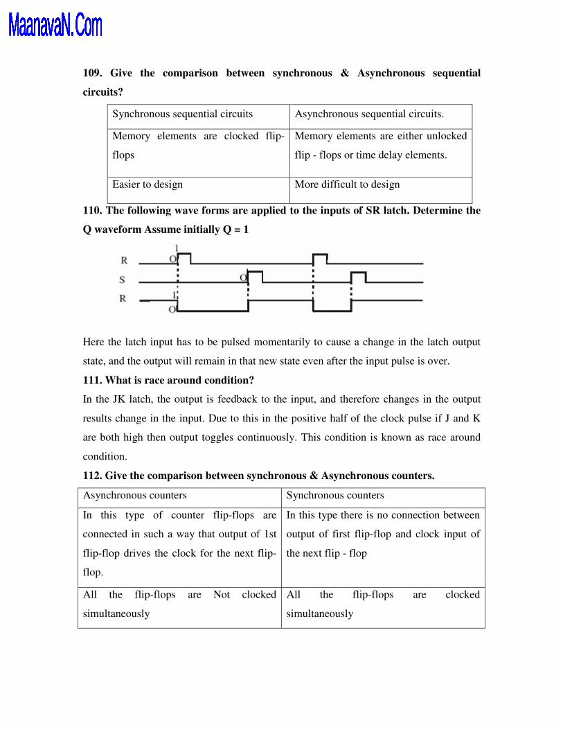
110. The following wave forms are applied to the inputs of SR latch. Determine the
Q waveform Assume initially Q = 1
Here the latch input has to be pulsed momentarily to cause a change in the latch output
state, and the output will remain in that new state even after the input pulse is over.
111. What is race around condition?
In the JK latch, the output is feedback to the input, and therefore changes in the output
results change in the input. Due to this in the positive half of the clock pulse if J and K
are both high then output toggles continuously. This condition is known as race around
condition.
112. Give the comparison between synchronous & Asynchronous counters.
Asynchronous counters Synchronous counters
In this type of counter flip-flops are
connected in such a way that output of 1st
flip-flop drives the clock for the next flip-
flop.
In this type there is no connection between
output of first flip-flop and clock input of
the next flip - flop
All the flip-flops are Not clocked
simultaneously
All the flip-flops are clocked
simultaneously
MaanavaN.ComMaanavaN.ComMaanavaN.ComMaanavaN.ComMaanavaN.ComMaanavaN.ComMaanavaN.ComMaanavaN.ComMaanavaN.ComMaanavaN.ComMaanavaN.Com
113. The tPd for each flip-flop is 50 ns. Determine the maximum operating frequency
for MOD - 32 ripple counter
f max (ripple) = 5 x 50 ns = 4 MHZ
114. What are secondary variables?
-present state variables in asynchronous sequential circuits
115. What are excitation variables?
-next state variables in asynchronous sequential circuits
116. What is fundamental mode sequential circuit?
-input variables changes if the circuit is stable
-inputs are levels, not pulses
-only one input can change at a given time
117. What is pulse mode circuit?
-inputs are pulses
-widths of pulses are long for circuit to respond to the input
-pulse width must not be so long that it is still present after the new state is
reached
118. What is the significance of state assignment?
In synchronous circuits-state assignments are made with the objective of circuit
reduction. Asynchronous circuits-its objective is to avoid critical races
119. When does race condition occur?
-two or more binary state variables change their value in response to the change in
i/p variable
120. What is non critical race?
-final stable state does not depend on the order in which the state variable changes
-race condition is not harmful
121. What is critical race?
-final stable state depends on the order in which the state variable changes
-race condition is harmful
122. When does a cycle occur?
-asynchronous circuit makes a transition through a series of unstable state
MaanavaN.ComMaanavaN.ComMaanavaN.ComMaanavaN.ComMaanavaN.ComMaanavaN.Com
123. What are the different techniques used in state assignment?
-shared row state assignment
-one hot state assignment
124. What are the steps for the design of asynchronous sequential circuit?
-construction of primitive flow table
-reduction of flow table
-state assignment is made
-realization of primitive flow table
125. What is hazard?
-unwanted switching transients
126. What is static 1 hazard?
-output goes momentarily 0 when it should remain at 1
127. What is static 0 hazard?
-output goes momentarily 1 when it should remain at 0
128. What is dynamic hazard?
-output changes 3 or more times when it changes from 1 to 0 or 0 to 1
129. What is the cause for essential hazards?
-unequal delays along 2 or more path from same input
130. What is flow table?
-state table of an synchronous sequential network
131. What is primitive flow chart?
-one stable state per row
132. What is combinational circuit?
Output depends on the given input. It has no storage element.
133. Define merger graph.
The merger graph is defined as follows. It contains the same number of vertices as the
state table contains states. A line drawn between the two state vertices indicates each
compatible state pair. It two states are incompatible no connecting line is drawn.
MaanavaN.ComMaanavaN.ComMaanavaN.ComMaanavaN.ComMaanavaN.ComMaanavaN.ComMaanavaN.ComMaanavaN.ComMaanavaN.Com
134. Define closed covering
A Set of compatibles is said to be closed if, for every compatible contained in the set, all
its implied compatibles are also contained in the set. A closed set of compatibles, which
contains all the states of M, is called a closed covering.
135. Define state table.
For the design of sequential counters we have to relate present states and next states. The
table, which represents the relationship between present states and next states, is called
state table.
136. Define total state
The combination of level signals that appear at the inputs and the outputs of the delays
define what is called the total state of the circuit.
137. What are the steps for the design of asynchronous sequential circuit?
1. Construction of a primitive flow table from the problem statement.
2. Primitive flow table is reduced by eliminating redundant states using the state
reduction
3. State assignment is made
4. The primitive flow table is realized using appropriate logic elements.
138. Define primitive flow table:
It is defined as a flow table which has exactly one stable state for each row in the table.
The design process begins with the construction of primitive flow table.
139. What are the types of asynchronous circuits?
1. Fundamental mode circuits
2. Pulse mode circuits
140. Give the comparison between state Assignment Synchronous circuit and state
assignment asynchronous circuit.
In synchronous circuit, the state assignments are made with the objective of circuit
reduction. In asynchronous circuits, the objective of state assignment is to avoid critical
races.
141. What are races?
When 2 or more binary state variables change their value in response to a change in an
input variable, race condition occurs in an asynchronous sequential circuit. In case of
MaanavaN.ComMaanavaN.ComMaanavaN.ComMaanavaN.ComMaanavaN.ComMaanavaN.Com
unequal delays, a race condition may cause the state variables to change in an
unpredictable manner.
142. Define non critical race.
If the final stable state that the circuit reaches does not depend on the order in which the
state variable changes, the race condition is not harmful and it is called a non critical race.
143. Define critical race?
If the final stable state depends on the order in which the state variable changes, the race
condition is harmful and it is called a critical race.
144. What is a cycle?
A cycle occurs when an asynchronous circuit makes a transition through a series of
unstable states. If a cycle does not contain a stable state, the circuit will go from one
unstable to stable to another, until the inputs are changed.
145. Write a short note on fundamental mode asynchronous circuit.
Fundamental mode circuit assumes that. The input variables change only when the circuit
is stable. Only one input variable can change at a given time and inputs are levels and not
pulses.
146. Write a short note on pulse mode circuit.
Pulse mode circuit assumes that the input variables are pulses instead of level. The width
of the pulses is long enough for the circuit to respond to the input and the pulse width
must not be so long that it is still present after the new state is reached.
147. Define secondary variables
The delay elements provide a short term memory for the sequential circuit. The present
state and next state variables in asynchronous sequential circuits are called secondary
variables.
148. Define flow table in asynchronous sequential circuit.
In asynchronous sequential circuit state table is known as flow table because of the
behavior of the asynchronous sequential circuit. The stage changes occur in independent
of a clock, based on the logic propagation delay, and cause the states to flow from one to
another.
MaanavaN.ComMaanavaN.ComMaanavaN.ComMaanavaN.Com
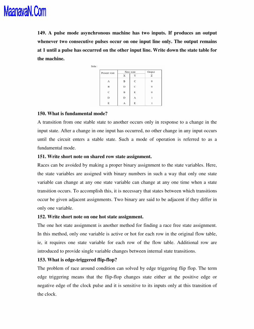
149. A pulse mode asynchronous machine has two inputs. If produces an output
whenever two consecutive pulses occur on one input line only. The output remains
at 1 until a pulse has occurred on the other input line. Write down the state table for
the machine.
150. What is fundamental mode?
A transition from one stable state to another occurs only in response to a change in the
input state. After a change in one input has occurred, no other change in any input occurs
until the circuit enters a stable state. Such a mode of operation is referred to as a
fundamental mode.
151. Write short note on shared row state assignment.
Races can be avoided by making a proper binary assignment to the state variables. Here,
the state variables are assigned with binary numbers in such a way that only one state
variable can change at any one state variable can change at any one time when a state
transition occurs. To accomplish this, it is necessary that states between which transitions
occur be given adjacent assignments. Two binary are said to be adjacent if they differ in
only one variable.
152. Write short note on one hot state assignment.
The one hot state assignment is another method for finding a race free state assignment.
In this method, only one variable is active or hot for each row in the original flow table,
ie, it requires one state variable for each row of the flow table. Additional row are
introduced to provide single variable changes between internal state transitions.
153. What is edge-triggered flip-flop?
The problem of race around condition can solved by edge triggering flip flop. The term
edge triggering means that the flip-flop changes state either at the positive edge or
negative edge of the clock pulse and it is sensitive to its inputs only at this transition of
the clock.
MaanavaN.ComMaanavaN.ComMaanavaN.ComMaanavaN.ComMaanavaN.ComMaanavaN.ComMaanavaN.ComMaanavaN.ComMaanavaN.ComMaanavaN.ComMaanavaN.ComMaanavaN.Com