Embed Size (px)
Citation preview

Copyright © Cirrus Logic, Inc. 2004(All Rights Reserved)
Cirrus Logic, Inc.www.cirrus.com
CS8405A
96 kHz Digital Audio Interface Transmitter
FeaturesComplete EIAJ CP1201, IEC-60958, AES3, S/PDIF-compatible Transmitter
+5.0 V Digital Supply (VD+) +3.3 V or 5.0 V Digital Interface (VL+) On-chip channel status and user bit buffer
memories allow block-sized updates. Flexible 3-wire Serial Digital Audio Input
Port Up to 96 kHz Frame Rate Microcontroller Write Access to Channel
Status and User Bit Data On-chip Differential Line Driver Generates CRC Codes and Parity Bits Standalone Mode Allows use Without a
Microcontroller
General DescriptionThe CS8405A is a monolithic CMOS device which en-codes and transmits audio data according to the AES3,IEC60958, S/PDIF, or EIAJ CP1201. The CS8405A ac-cepts audio and digital data, which is then multiplexed,encoded, and driven onto a cable.
The audio data is input through a configurable, 3-wire in-put port. The channel status and user bit data are inputthrough an SPI or I²C microcontroller port, and may beassembled in block-sized buffers. For systems with nomicrocontroller, a standalone mode allows direct accessto channel status and user bit data pins.
Target applications include A/V Receivers, CD-R, DVDreceivers, digital mixing consoles, effects processors,set-top boxes, and computer or automotive audiosystems.
ORDERING INFORMATION
CS8405A-CS 28-pin SOIC -10 to +70°CCS8405A-CZ 28-pin TSSOP -10 to +70°CCS8405A-CZZ, Lead Free 28-pin TSSOP -10 to +70°CCS8405A-IS 28-pin SOIC -40 to +85°CCS8405A-IZ 28-pin TSSOP -40 to +85°CCDB8415A Evaluation Board
I
SerialAudioInput
Misc.Control
AES3S/PDIFEncoder
C & U bitDataBuffer
ControlPort &Registers
OutputClockGenerator
RXP
ILRCKISCLK
SDIN
TXP
TXN
RST OMCKU TCBL SDA/CDOUT
SCL/CCLK
AD1/CDIN
AD0/CS
INT
VL+ DGND
Driver
AD2H/S
VD+
1
Aug ‘04DS469F2
CS8405A
TABLE OF CONTENTS1. CHARACTERISTICS AND SPECIFICATIONS ........................................................................ 4
SPECIFIED OPERATING CONDITIONS ................................................................................. 4ABSOLUTE MAXIMUM RATINGS ........................................................................................... 4DC ELECTRICAL CHARACTERISTICS................................................................................... 5DIGITAL INPUT CHARACTERISTICS ..................................................................................... 5DIGITAL INTERFACE SPECIFICATIONS................................................................................ 5TRANSMITTER CHARACTERISTICS ..................................................................................... 5SWITCHING CHARACTERISTICS .......................................................................................... 6SWITCHING CHARACTERISTICS - SERIAL AUDIO PORTS................................................. 6SWITCHING CHARACTERISTICS - CONTROL PORT - SPI MODE...................................... 8SWITCHING CHARACTERISTICS - CONTROL PORT - I²C MODE....................................... 9
2. TYPICAL CONNECTION DIAGRAM ...................................................................................... 103. GENERAL DESCRIPTION ..................................................................................................... 11
3.1 AES3 and S/PDIF Standards Documents ........................................................................ 114. THREE-WIRE SERIAL INPUT AUDIO PORT ........................................................................ 115. AES3 TRANSMITTER ............................................................................................................ 13
5.1 Transmitted Frame and Channel Status Boundary Timing .............................................. 135.2 TXN and TXP Drivers ...................................................................................................... 135.3 Mono Mode Operation ..................................................................................................... 13
6. CONTROL PORT DESCRIPTION AND TIMING .................................................................... 156.1 SPI Mode ......................................................................................................................... 156.2 I²C Mode .......................................................................................................................... 156.3 Interrupts .......................................................................................................................... 16
7. CONTROL PORT REGISTER SUMMARY ........................................................................... 177.1 Memory Address Pointer (MAP) ....................................................................................... 17
8. CONTROL PORT REGISTER BIT DEFINITIONS .................................................................. 188.1 Control 1 (01h) .................................................................................................................. 188.2 Control 2 (02h) .................................................................................................................. 188.3 Data Flow Control (03h).................................................................................................... 198.4 Clock Source Control (04h)............................................................................................... 198.5 Serial Audio Input Port Data Format (05h)........................................................................ 208.6 Interrupt 1 Status (07h) (Read Only)................................................................................. 218.7 Interrupt 2 Status (08h) (Read Only)................................................................................. 218.8 Interrupt 1 Mask (09h)....................................................................................................... 218.9 Interrupt 1 Mode MSB (0Ah) and Interrupt 1 Mode LSB (0Bh) ......................................... 228.10 Interrupt 2 Mask (0Ch) .................................................................................................... 228.11 Interrupt 2 Mode MSB (0Dh) and Interrupt Mode 2 LSB (0Eh)....................................... 228.12 Channel Status Data Buffer Control (12h) ...................................................................... 238.13 User Data Buffer Control (13h) ....................................................................................... 238.14 Channel Status bit or User bit Data Buffer (20h - 37h) ................................................... 248.15 CS8405A I.D. and Version Register (7Fh) (Read Only) ................................................. 24
9. PIN DESCRIPTION - SOFTWARE MODE .......................................................................... 2510. HARDWARE MODE ............................................................................................................. 27
10.1 Channel Status, User and Validity Data ......................................................................... 2710.2 Serial Audio Port Formats .............................................................................................. 27
11. PIN DESCRIPTION - HARDWARE MODE ....................................................................... 2912. APPLICATIONS .................................................................................................................... 31
12.1 Reset, Power Down and Start-up .................................................................................. 3112.2 ID Code and Revision Code .......................................................................................... 3112.3 Power Supply, Grounding, and PCB layout ................................................................... 3112.4 Synchronization of Multiple CS8405As .......................................................................... 31
13. PACKAGE DIMENSIONS ................................................................................................... 32
2 DS469F2
CS8405A
14. APPENDIX A: EXTERNAL AES3/SPDIF/IEC60958 TRANSMITTER AND RECEIVER COMPO-NENTS .................................................................................................................................. 3414.1 AES3 Transmitter External Components ....................................................................... 3414.2 Isolating Transformer Requirements ............................................................................. 34
15. APPENDIX B: CHANNEL STATUS AND USER DATA BUFFER MANAGEMENT ........... 3515.1 AES3 Channel Status(C) Bit Management .................................................................... 35
15.1.1 Accessing the E buffer ...................................................................................... 3515.1.2 Serial Copy Management System (SCMS) ....................................................... 3615.1.3 Channel Status Data E Buffer Access .............................................................. 36
15.2 AES3 User (U) Bit Management .................................................................................... 3615.2.1 Mode 1: Transmit All Zeros ............................................................................... 3615.2.2 Mode 2: Block Mode ......................................................................................... 36
16. REVISION HISTORY ............................................................................................................ 37
LIST OF FIGURESFigure 1. Audio Port Master Mode Timing ...................................................................................... 7Figure 2. Audio Port Slave Mode and Data Input Timing................................................................ 7Figure 3. SPI Mode timing............................................................................................................... 8Figure 4. I²C Mode timing................................................................................................................ 9Figure 5. Recommended Connection Diagram for Software Mode .............................................. 10Figure 6. Serial Audio Input Example Formats ............................................................................. 12Figure 7. AES3 Transmitter Timing for C, U, and V Pin Input Data .............................................. 14Figure 8. Control Port Timing in SPI Mode ................................................................................... 15Figure 9. Control Port Timing in I²C Mode .................................................................................... 16Figure 10. Hardware Mode ........................................................................................................... 27Figure 11. Professional Output Circuit .......................................................................................... 34Figure 12. Consumer Output Circuit ............................................................................................. 34Figure 13. TTL/CMOS Output Circuit............................................................................................ 34Figure 14. Channel Status Data Buffer Structure.......................................................................... 35Figure 15. Flowchart for Writing the E Buffer ................................................................................ 35
LIST OF TABLESTable 1. Control Register Map Summary...................................................................................... 17Table 2. Hardware Mode COPY/C and ORIG pin functions ......................................................... 27Table 3. Hardware Mode Serial Audio Port Format Selection ...................................................... 28Table 4. Equivalent Register Settings of Serial Audio Input Formats Available in Hardware Mode28Table 5. Revision History .............................................................................................................. 37
DS469F2 3
CS8405A
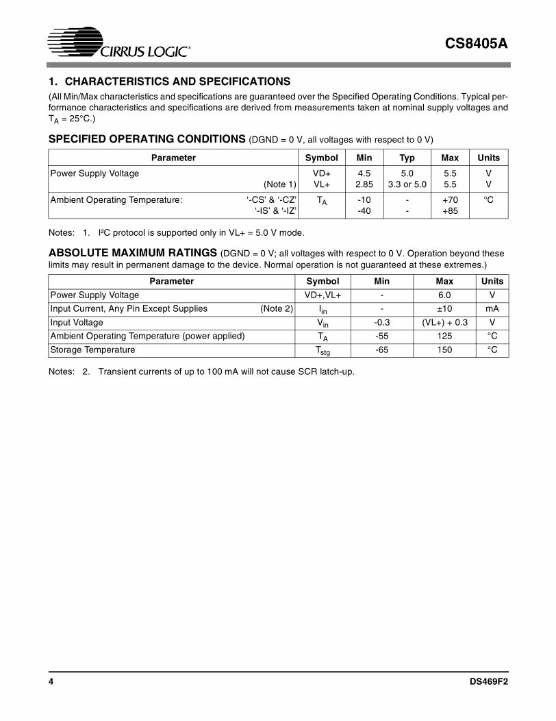
1. CHARACTERISTICS AND SPECIFICATIONS(All Min/Max characteristics and specifications are guaranteed over the Specified Operating Conditions. Typical per-formance characteristics and specifications are derived from measurements taken at nominal supply voltages andTA = 25°C.)
SPECIFIED OPERATING CONDITIONS (DGND = 0 V, all voltages with respect to 0 V)
Notes: 1. I²C protocol is supported only in VL+ = 5.0 V mode.
ABSOLUTE MAXIMUM RATINGS (DGND = 0 V; all voltages with respect to 0 V. Operation beyond these limits may result in permanent damage to the device. Normal operation is not guaranteed at these extremes.)
Notes: 2. Transient currents of up to 100 mA will not cause SCR latch-up.
Parameter Symbol Min Typ Max Units
Power Supply Voltage(Note 1)
VD+VL+
4.52.85
5.03.3 or 5.0
5.55.5
VV
Ambient Operating Temperature: ‘-CS’ & ‘-CZ’‘-IS’ & ‘-IZ’
TA -10-40
--
+70+85
°C
Parameter Symbol Min Max Units
Power Supply Voltage VD+,VL+ - 6.0 V
Input Current, Any Pin Except Supplies (Note 2) Iin - ±10 mA
Input Voltage Vin -0.3 (VL+) + 0.3 V
Ambient Operating Temperature (power applied) TA -55 125 °C
Storage Temperature Tstg -65 150 °C
4 DS469F2

CS8405A
DC ELECTRICAL CHARACTERISTICS (DGND = 0 V; all voltages with respect to 0 V.)
Notes: 3. Power Down Mode is defined as RST = LO with all clocks and data lines held static.
4. Normal operation is defined as RST = HI.
DIGITAL INPUT CHARACTERISTICS
DIGITAL INTERFACE SPECIFICATIONS (DGND = 0 V; all voltages with respect to 0 V.)
Notes: 5. At 5.0 V mode, VIL = 0.8 V (Max), at 3.3 V mode, VIL =0.4 V (Max).
TRANSMITTER CHARACTERISTICS
Parameters Symbol Min Typ Max Units
Power-down Mode (Note 3)
Supply Current in power down VD+VL+ = 3.3 VVL+ = 5.0 V
---
206060
---
µAµAµA
Normal Operation (Note 4)
Supply Current at 48 kHz frame rate VD+VL+ = 3.3 VVL+ = 5.0 V
---
6.330.146.5
---
mAmAmA
Supply Current at 96 kHz frame rate VD+VL+ = 3.3 VVL+ = 5.0 V
---
6.644.876.6
---
mAmAmA
Parameters Symbol Min Typ Max Units
Input Leakage Current Iin - ±1 ±10 µA
Parameters Symbol Min Max Units
High-Level Output Voltage (IOH = -3.2 mA), except TXP/TXN VOH (VL+) - 1.0 - V
Low-Level Output Voltage (IOL = 3.2 mA), except TXP/TXN VOL - 0.4 V
High-Level Output Voltage, TXP, TXN (23 mA at VL+ = 5.0 V)(15.2 mA at VL+ = 3.3 V)
(VL+) - 0.7(VL+) - 0.7
--
VV
Low-Level Output Voltage, TXP, TXN (23 mA at VL+ = 5.0 V)(15.2 mA at VL+ = 3.3 V)
--
0.70.7
VV
High-Level Input Voltage VIH 2.0 (VL+) + 0.3 V
Low-Level Input Voltage (Note 5) VIL -0.3 0.4/0.8 V
Parameters Symbol Min Typ Max Units
TXP Output Resistance VL+ = 5.0 VVL+ = 3.3 V
RTXP --
2640
--
ΩΩ
TXN Output Resistance VL+ = 5.0 VVL+ = 3.3 V
RTXN --
2640
--
ΩΩ
DS469F2 5
CS8405A
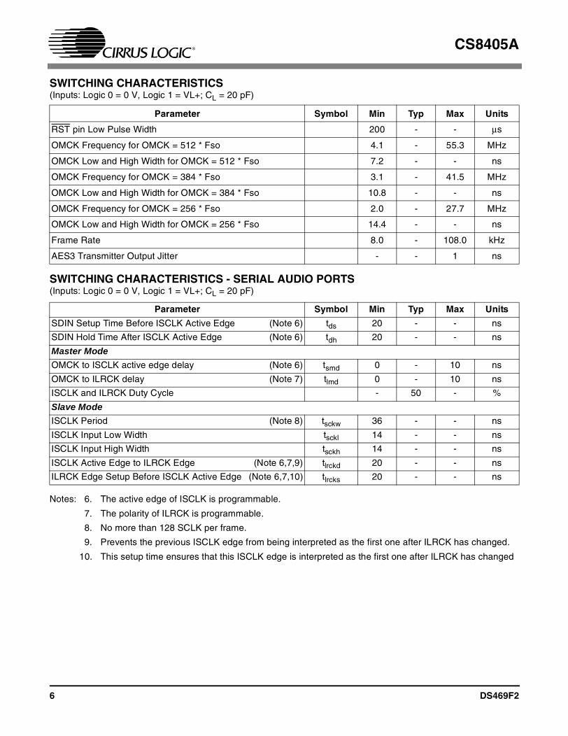
SWITCHING CHARACTERISTICS (Inputs: Logic 0 = 0 V, Logic 1 = VL+; CL = 20 pF)
SWITCHING CHARACTERISTICS - SERIAL AUDIO PORTS (Inputs: Logic 0 = 0 V, Logic 1 = VL+; CL = 20 pF)
Notes: 6. The active edge of ISCLK is programmable.
7. The polarity of ILRCK is programmable.
8. No more than 128 SCLK per frame.
9. Prevents the previous ISCLK edge from being interpreted as the first one after ILRCK has changed.
10. This setup time ensures that this ISCLK edge is interpreted as the first one after ILRCK has changed
Parameter Symbol Min Typ Max Units
RST pin Low Pulse Width 200 - - µs
OMCK Frequency for OMCK = 512 * Fso 4.1 - 55.3 MHz
OMCK Low and High Width for OMCK = 512 * Fso 7.2 - - ns
OMCK Frequency for OMCK = 384 * Fso 3.1 - 41.5 MHz
OMCK Low and High Width for OMCK = 384 * Fso 10.8 - - ns
OMCK Frequency for OMCK = 256 * Fso 2.0 - 27.7 MHz
OMCK Low and High Width for OMCK = 256 * Fso 14.4 - - ns
Frame Rate 8.0 - 108.0 kHz
AES3 Transmitter Output Jitter - - 1 ns
Parameter Symbol Min Typ Max Units
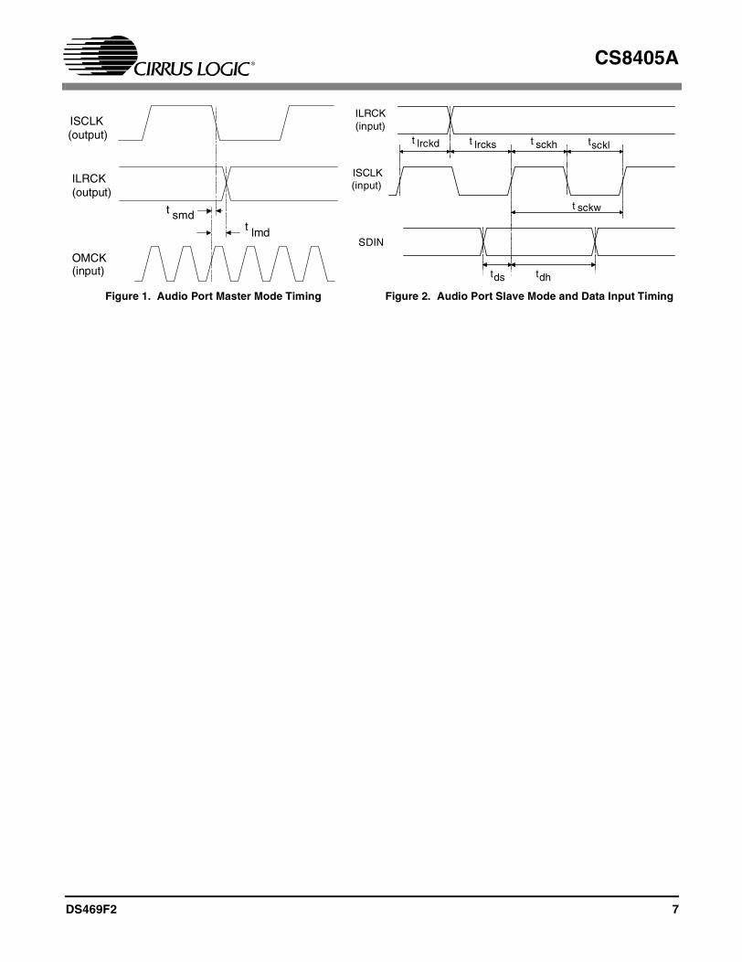
SDIN Setup Time Before ISCLK Active Edge (Note 6) tds 20 - - ns
SDIN Hold Time After ISCLK Active Edge (Note 6) tdh 20 - - ns
Master Mode
OMCK to ISCLK active edge delay (Note 6) tsmd 0 - 10 ns
OMCK to ILRCK delay (Note 7) tlmd 0 - 10 ns
ISCLK and ILRCK Duty Cycle - 50 - %
Slave Mode
ISCLK Period (Note 8) tsckw 36 - - ns
ISCLK Input Low Width tsckl 14 - - ns
ISCLK Input High Width tsckh 14 - - ns
ISCLK Active Edge to ILRCK Edge (Note 6,7,9) tlrckd 20 - - ns
ILRCK Edge Setup Before ISCLK Active Edge (Note 6,7,10) tlrcks 20 - - ns
6 DS469F2
CS8405A
ISCLK
ILRCK
(output)
(output)
OMCK(input)
t smdt lmd
sckh sckl
sckwt
tt(input)
(input)
SDIN
dhtdst
lrckstlrckdt
ISCLK
ILRCK
Figure 1. Audio Port Master Mode Timing Figure 2. Audio Port Slave Mode and Data Input Timing
DS469F2 7
CS8405A
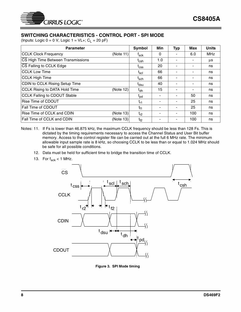
SWITCHING CHARACTERISTICS - CONTROL PORT - SPI MODE (Inputs: Logic 0 = 0 V, Logic 1 = VL+; CL = 20 pF)
Notes: 11. If Fs is lower than 46.875 kHz, the maximum CCLK frequency should be less than 128 Fs. This is dictated by the timing requirements necessary to access the Channel Status and User Bit buffer memory. Access to the control register file can be carried out at the full 6 MHz rate. The minimum allowable input sample rate is 8 kHz, so choosing CCLK to be less than or equal to 1.024 MHz should be safe for all possible conditions.
12. Data must be held for sufficient time to bridge the transition time of CCLK.
13. For fsck < 1 MHz.
Parameter Symbol Min Typ Max Units
CCLK Clock Frequency (Note 11) fsck 0 - 6.0 MHz
CS High Time Between Transmissions tcsh 1.0 - - µs
CS Falling to CCLK Edge tcss 20 - - ns
CCLK Low Time tscl 66 - - ns
CCLK High Time tsch 66 - - ns
CDIN to CCLK Rising Setup Time tdsu 40 - - ns
CCLK Rising to DATA Hold Time (Note 12) tdh 15 - - ns
CCLK Falling to CDOUT Stable tpd - - 50 ns
Rise Time of CDOUT tr1 - - 25 ns
Fall Time of CDOUT tf1 - - 25 ns
Rise Time of CCLK and CDIN (Note 13) tr2 - - 100 ns
Fall Time of CCLK and CDIN (Note 13) tf2 - - 100 ns
t r2 t f2
t dsu t dh
t scht scl
CS
CCLK
CDIN
t css
t pd
CDOUT
tcsh
Figure 3. SPI Mode timing
8 DS469F2

CS8405A
SWITCHING CHARACTERISTICS - CONTROL PORT - I²C MODE (Note 14, Inputs: Logic 0 = 0 V, Logic 1 = VL+; CL = 20 pF)
Notes: 14. I²C protocol is supported only in VL+ = 5.0 V mode.
15. Data must be held for sufficient time to bridge the 300 ns transition time of SCL.
Parameter Symbol Min Typ Max Units
SCL Clock Frequency fscl - - 100 kHz
Bus Free Time Between Transmissions tbuf 4.7 - - µs
Start Condition Hold Time (prior to first clock pulse) thdst 4.0 - - µs
Clock Low Time tlow 4.7 - - µs
Clock High Time thigh 4.0 - - µs
Setup Time for Repeated Start Condition tsust 4.7 - - µs
SDA Hold Time from SCL Falling (Note 15) thdd 0 - - µs
SDA Setup Time to SCL Rising tsud 250 - - ns
Rise Time of Both SDA and SCL Lines tr - - 25 ns
Fall Time of Both SDA and SCL Lines tf - - 25 ns
Setup Time for Stop Condition tsusp 4.7 - - µs
t buf t hdstt hdst
tlow
t r
t f
thdd
t high
t sud tsust
t susp
Stop Start Start StopRepeated
SDA
SCL
Figure 4. I²C Mode timing
DS469F2 9
CS8405A
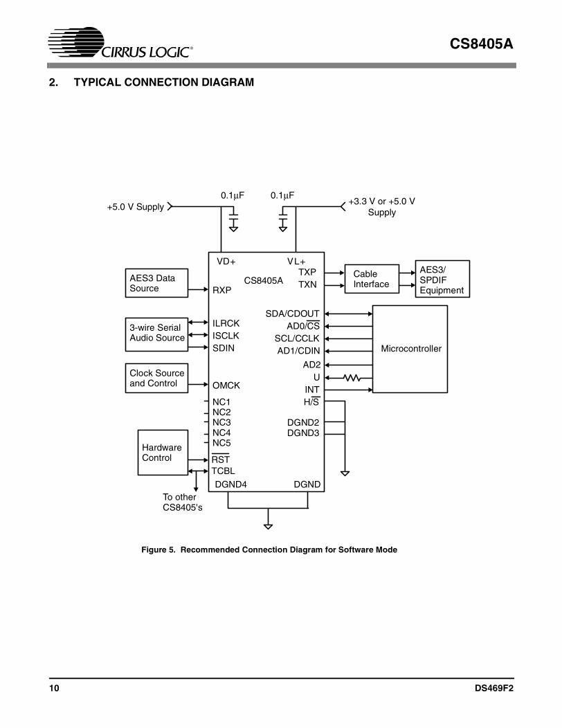
2. TYPICAL CONNECTION DIAGRAM
3-wire SerialAudio Source
ILRCKISCLKSDIN
Clock Sourceand Control OMCK
HardwareControl RST
TCBL
To otherCS8405's
CableInterface
AES3/SPDIFEquipment
TXPTXN
SDA/CDOUTAD0/CS
SCL/CCLKAD1/CDIN
UINT
VD+ VL+
0.1 Fµ
H/S
DGNDDGND4
0.1 Fµ
AD2
RXP
DGND2DGND3
NC1NC2NC3NC4NC5
CS8405A
+3.3 V or +5.0 VSupply
+5.0 V Supply
Microcontroller
AES3 DataSource
Figure 5. Recommended Connection Diagram for Software Mode
10 DS469F2

CS8405A
3. GENERAL DESCRIPTIONThe CS8405A is a monolithic CMOS device whichencodes and transmits audio data according to theAES3, IEC60958, S/PDIF, and EIAJ CP1201 inter-face standards. The CS8405A accepts audio,channel status and user data, which is then multi-plexed, encoded, and driven onto a cable.
The audio data is input through a configurable,3-wire input port. The channel status bits and userbit data are input through an SPI or I²C Mode mi-crocontroller port and may be assembled in sepa-rate block sized buffers.
For systems with no microcontroller, a stand alonemode allows direct access to channel status anduser data input pins.
Target applications include CD-R, DAT, DVD, MDand VTR equipment, mixing consoles, digital audiotransmission equipment, high quality A/D convert-ers, effects processors, set-top TV boxes, andcomputer audio systems.
Figure 5 shows the supply and external connec-tions to the CS8405A when configured for opera-tion with a microcontroller.
3.1 AES3 and S/PDIF Standards Documents
This data sheet assumes that the user is familiarwith the AES3 and S/PDIF data formats. It is advis-able to have current copies of the AES3 andIEC60958 specifications on hand for easy refer-ence.
The latest AES3 standard is available from the Au-dio Engineering Society or ANSI at www.aes.org orwww.ansi.org. Obtain the latest IEC60958 stan-dard from ANSI or from the International Electro-technical Commission at www.iec.ch. The latestEIAJ CP-1201 standard is available from the Jap-anese Electronics Bureau.
Crystal Application Note 22: Overview of DigitalAudio Interface Data Structures contains a useful
tutorial on digital audio specifications, but it shouldnot be considered a substitute for the standards.
The paper An Understanding and Implementationof the SCMS Serial Copy Management System forDigital Audio Transmission, by Clifton Sanchez, isan excellent tutorial on SCMS. It is available fromthe AES as preprint 3518.
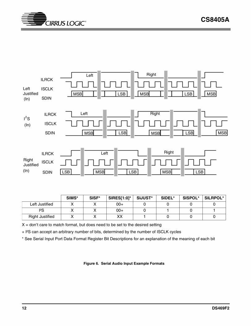
4.THREE-WIRE SERIAL INPUT AUDIO PORT
A 3-wire serial audio input port is provided. The in-terface format can be adjusted to suit the attacheddevice through the control registers. The followingparameters are adjustable:
• Master or slave
• Serial clock frequency
• Audio data resolution
• Left or right justification of the data relative toleft/right clock
• Optional one-bit cell delay of the first data bit
• Polarity of the bit clock
• Polarity of the left/right clock. (By setting theappropriate control bits, many formats are pos-sible).
Figure 6 shows a selection of common input for-mats with the corresponding control bit settings.
In master mode, the left/right clock and the serialbit clock are outputs, derived from the OMCK inputpin master clock.
In slave mode, the left/right clock and the serial bitclock are inputs. The left/right clock must be syn-chronous to the OMCK master clock, but the serialbit clock can be asynchronous and discontinuous ifrequired. The left/right clock should be continuous,but the duty cycle can be less than the specifiedtypical value of 50% if enough serial clocks arepresent in each phase to clock all the data bits.
DS469F2 11
CS8405A
ILRCK
ISCLK
SDIN
2
LeftJustified(In)
MSB LSB
Left Right
MSB
I S
(In)
RightJustified(In)
MSB LSB MSB LSB MSB
Left Right
MSB LSB
MSB LSB
Left Right
LSB MSB LSB
ILRCK
ISCLK
SDIN
ILRCK
ISCLK
SDIN
Figure 6. Serial Audio Input Example Formats
X = don’t care to match format, but does need to be set to the desired setting
+ I²S can accept an arbitrary number of bits, determined by the number of ISCLK cycles
* See Serial Input Port Data Format Register Bit Descriptions for an explanation of the meaning of each bit
SIMS* SISF* SIRES[1:0]* SIJUST* SIDEL* SISPOL* SILRPOL*
Left Justified X X 00+ 0 0 0 0
I²S X X 00+ 0 1 0 1
Right Justified X X XX 1 0 0 0
12 DS469F2
CS8405A
5. AES3 TRANSMITTERThe CS8405A includes an AES3 digital audiotransmitter. A comprehensive buffering schemeprovides write access to the channel status anduser data. This buffering scheme is described in“Appendix B: Channel Status and User Data BufferManagement” on page 35.
The AES3 transmitter encodes and transmits au-dio and digital data according to the AES3,IEC60958 (S/PDIF), and EIAJ CP-1201 interfacestandards. Audio and control data are multiplexedtogether and bi-phase mark encoded. The result-ing bit stream is driven to an output connector ei-ther directly or through a transformer. Thetransmitter is clocked from the clock input pin,OM-K. If OMCK is asynchronous to the datasource, an interrupt bit (TSLIP) is provided that willgo high every time a data sample is dropped or re-peated. Be aware that the pattern of slips does nothave hysteresis and so the occurrence of the inter-rupt condition is not deterministic.
The channel status (C) and user (U) bits in thetransmitted data stream are taken from storage ar-eas within the CS8405A. The user can manuallyaccess the internal storage or configure theCS8405A to run in one of several automaticmodes. “Appendix B: Channel Status and UserData Buffer Management” on page 35 provides de-tailed descriptions of each automatic mode and de-scribes methods of manually accessing thestorage areas. The transmitted user bit data canoptionally be input through the U pin, under thecontrol of a control port register bit. Figure 7 showsthe timing requirements for inputting U datathrough the U pin.
5.1 Transmitted Frame and Channel Status Boundary Timing
The TCBL pin is used to control or indicate the startof transmitted channel status block boundaries andmay be an input or an output.
In some applications, it may be necessary to con-trol the precise timing of the transmitted AES3frame boundaries. This may be achieved in twoways:
a) With TCBL set to input, driving TCBL high for >3OMCK clocks will cause a frame start, as well as anew channel status block start.
b) If the serial audio input port is in slave mode andTCBL is set to output, the start of the A channelsub-frame will be aligned with the leading edge ofILRCK.
5.2 TXN and TXP DriversThe line drivers are low skew, low impedance, dif-ferential outputs capable of driving cables directly.Both drivers are set to ground during reset (RST =low), when no AES3 transmit clock is provided,and optionally under the control of a register bit.The CS8405A also allows immediate muting of theAES3 transmitter audio data through a control reg-ister bit.
External components are used to terminate andisolate the external cable from the CS8405A.These components are detailed in “Appendix A:External AES3/SPDIF/IEC60958 Transmitter andReceiver Components” on page 34.
5.3 Mono Mode OperationAn AES3 stream may be used in more than oneway to transmit 96 kHz sample rate data. Onemethod is to double the frame rate of the currentformat. This results in a stereo signal with a samplerate of 96 kHz, carried over a single twisted paircable. An alternate method is implemented usingthe two sub-frames in a 48 kHz frame rate AES3signal to carry consecutive samples of a mono sig-nal, resulting in a 96 kHz sample rate stream. Thisallows older equipment, whose AES3 transmittersand receivers are not rated for 96 kHz frame rateoperation, to handle 96 kHz sample rate informa-tion. In this “mono mode”, two AES3 cables areneeded for stereo data transfer. The CS8405A of-fers mono mode operation. The CS8405A is set tomono mode by the MMT control bit.
In mono mode, the input port will run at the audiosample rate (Fs), while the AES3 transmitter framerate will be at Fs/2. Consecutive left or right chan-nel serial audio data samples may be selected fortransmission on the A and B sub-frames, and thechannel status block transmitted is also selectable.
Using mono mode is only necessary if the incom-ing audio sample rate is already at 96 kHz andcontains both left and right audio data words. The“mono mode” AES3 output stream may also beachieved by keeping the CS8405A in normal
DS469F2 13

CS8405A
stereo mode, and placing consecutive audio sam-ples in the left and right positions in an incoming48 kHz word rate data stream.
VCU[0] VCU[1] VCU[2] VCU[3] VCU[4]
TCBLIn or OutVLRCK
VCUInput
Data [4] Data [5] Data [6] Data [7] Data [8]SDINInput
Data [0] Data [1] Data [2] Data [3] Data [4]TXP(N)Output
Z Y X Y X
AES3 Transmitter in Stereo mode
U[0] U[2]
TCBLIn or Out
VLRCK
UInput
Data [4] Data [5] Data [6] Data [7] Data [8]SDINInput
Data [0]* Data [2]* Data [4]*TXP(N)Output
Z Y X
* Assume MMTLR = 0
Tsetup => 7.5% AES3 frame timeThold = 0
Tsetup Thold
Data [1]* Data [3]* Data [5]*TXP(N)Output
Z Y X
AES3 Transmitter in Mono mode* Assume MMTLR = 1
Tsetup => 15% AES3 frame timeThold = 0
VLRCK is a virtual word clock, which may not exist, and is used to illustrate the CUV timing.VLRCK duty cycle is 50%.In stereo mode, VLRCK frequency = AES3 frame rate. In mono mode, ALRCK frequency = 2xAES3 frame rate.If the serial audio input port is on slave mode and TCBL is an output, then VLRCK=ILRCK if SILRPOL=0 andVLRCK= ILRCK if SILRPOL =1.If the serial audio input port is in master mode and TCBL is an input, then VLRCK=ILRCK if SILRPOL=0 andVLRCK= ILRCK if SILRPOL =1.
Tth
Tth > 3OMCK if TCBL is Input
Tth > 3OMCK if TCBL is Input
Tth
Figure 7. AES3 Transmitter Timing for C, U, and V Pin Input Data
14 DS469F2

CS8405A
6. CONTROL PORT DESCRIPTION AND TIMING
The control port is used to access the registers, al-lowing the CS8405A to be configured for the de-sired operational modes and formats. In addition,Channel Status and User data may be read andwritten through the control port. The operation ofthe control port may be completely asynchronouswith respect to the audio sample rate.
The control port has two modes: SPI and I²C, withthe CS8405A acting as a slave device. SPI modeis selected if there is a high to low transition on theAD0/CS pin after the RST pin has been broughthigh. I²C mode is selected by connecting theAD0/CS pin to VL+ or DGND, thereby permanentlyselecting the desired AD0 bit address state.
6.1 SPI ModeIn SPI mode, CS is the CS8405A chip select sig-nal, CCLK is the control port bit clock (input into theCS8405A from the microcontroller); CDIN is the in-put data line from the microcontroller; and CDOUTis the output data line to the microcontroller. Datais clocked in on the rising edge of CCLK and out onthe falling edge.
Figure 8 shows the operation of the control port inSPI mode. To write to a register, bring CS low. Thefirst seven bits on CDIN form the chip address andmust be 0010000. The eighth bit is a read/write in-dicator (R/W), which should be low to write. Thenext eight bits form the Memory Address Pointer(MAP), which is set to the address of the register
that is to be updated. The next eight bits are thedata which will be placed into the register designat-ed by the MAP. During writes, the CDOUT outputstays in the Hi-Z state. It may be externally pulledhigh or low with a 47 kΩ resistor, if desired.
There is a MAP auto increment capability, enabledby the INCR bit in the MAP register. If INCR is azero, the MAP will stay constant for successiveread or writes. If INCR is set to a 1, then the MAPwill auto increment after each byte is read orwritten, allowing block reads or writes ofsuccessive registers.
To read a register, the MAP has to be set to thecorrect address by executing a partial write cyclewhich finishes (CS high) immediately after theMAP byte. The MAP auto increment bit (INCR)may be set or not, as desired. To begin a read,bring CS low, send out the chip address and setthe read/write bit (R/W) high. The next falling edgeof CCLK will clock out the MSB of the addressedregister (CDOUT will leave the high impedancestate). If the MAP auto increment bit is set to 1, thedata for successive registers will appearconsecutively.
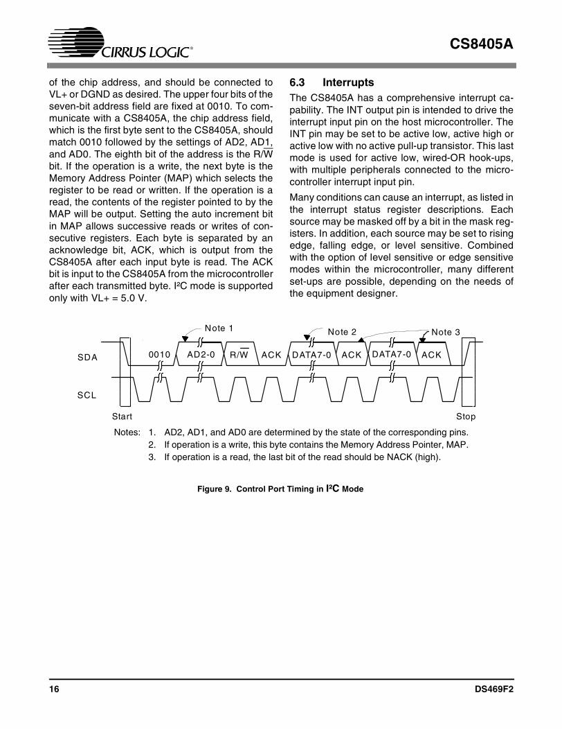
6.2 I²C ModeIn I²C Mode, SDA is a bidirectional data line. Datais clocked into and out of the part by the clock,SCL, with the clock to data relationship as shownin Figure 9. There is no CS pin. Each individualCS8405A is given a unique address. Pins AD0,AD1, and AD2 form the three least significant bits
M A P
MSB LSB
DATA
b y te 1 b y te n
R/W R/W
A D D R E S SC H IP
ADDRESSC H IP
C D IN
C C L K
CS
C D O U T MSB LSB MSB LSB
00100000010000
MAP = Memory Address Pointer, 8 bits, MSB first
High Impedance
Figure 8. Control Port Timing in SPI Mode
DS469F2 15
CS8405A
of the chip address, and should be connected toVL+ or DGND as desired. The upper four bits of theseven-bit address field are fixed at 0010. To com-municate with a CS8405A, the chip address field,which is the first byte sent to the CS8405A, shouldmatch 0010 followed by the settings of AD2, AD1,and AD0. The eighth bit of the address is the R/Wbit. If the operation is a write, the next byte is theMemory Address Pointer (MAP) which selects theregister to be read or written. If the operation is aread, the contents of the register pointed to by theMAP will be output. Setting the auto increment bitin MAP allows successive reads or writes of con-secutive registers. Each byte is separated by anacknowledge bit, ACK, which is output from theCS8405A after each input byte is read. The ACKbit is input to the CS8405A from the microcontrollerafter each transmitted byte. I²C mode is supportedonly with VL+ = 5.0 V.
6.3 Interrupts The CS8405A has a comprehensive interrupt ca-pability. The INT output pin is intended to drive theinterrupt input pin on the host microcontroller. TheINT pin may be set to be active low, active high oractive low with no active pull-up transistor. This lastmode is used for active low, wired-OR hook-ups,with multiple peripherals connected to the micro-controller interrupt input pin.
Many conditions can cause an interrupt, as listed inthe interrupt status register descriptions. Eachsource may be masked off by a bit in the mask reg-isters. In addition, each source may be set to risingedge, falling edge, or level sensitive. Combinedwith the option of level sensitive or edge sensitivemodes within the microcontroller, many differentset-ups are possible, depending on the needs ofthe equipment designer.
SDA
SCL
0010 AD2-0 R/W
Start
ACK DATA7-0 ACK DATA7-0 ACK
Stop
Note 2Note 1 Note 3
Figure 9. Control Port Timing in I²C Mode
Notes: 1. AD2, AD1, and AD0 are determined by the state of the corresponding pins.2. If operation is a write, this byte contains the Memory Address Pointer, MAP.3. If operation is a read, the last bit of the read should be NACK (high).
16 DS469F2
CS8405A
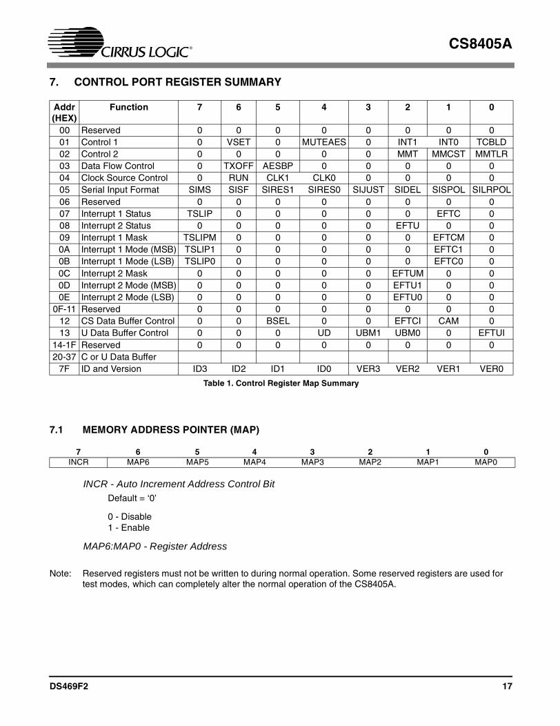
7. CONTROL PORT REGISTER SUMMARY
7.1 MEMORY ADDRESS POINTER (MAP)
INCR - Auto Increment Address Control BitDefault = ‘0’
0 - Disable1 - Enable
MAP6:MAP0 - Register Address
Note: Reserved registers must not be written to during normal operation. Some reserved registers are used for test modes, which can completely alter the normal operation of the CS8405A.
Addr (HEX)
Function 7 6 5 4 3 2 1 0
00 Reserved 0 0 0 0 0 0 0 001 Control 1 0 VSET 0 MUTEAES 0 INT1 INT0 TCBLD02 Control 2 0 0 0 0 0 MMT MMCST MMTLR03 Data Flow Control 0 TXOFF AESBP 0 0 0 0 004 Clock Source Control 0 RUN CLK1 CLK0 0 0 0 005 Serial Input Format SIMS SISF SIRES1 SIRES0 SIJUST SIDEL SISPOL SILRPOL06 Reserved 0 0 0 0 0 0 0 007 Interrupt 1 Status TSLIP 0 0 0 0 0 EFTC 008 Interrupt 2 Status 0 0 0 0 0 EFTU 0 009 Interrupt 1 Mask TSLIPM 0 0 0 0 0 EFTCM 00A Interrupt 1 Mode (MSB) TSLIP1 0 0 0 0 0 EFTC1 00B Interrupt 1 Mode (LSB) TSLIP0 0 0 0 0 0 EFTC0 00C Interrupt 2 Mask 0 0 0 0 0 EFTUM 0 00D Interrupt 2 Mode (MSB) 0 0 0 0 0 EFTU1 0 00E Interrupt 2 Mode (LSB) 0 0 0 0 0 EFTU0 0 0
0F-11 Reserved 0 0 0 0 0 0 0 012 CS Data Buffer Control 0 0 BSEL 0 0 EFTCI CAM 013 U Data Buffer Control 0 0 0 UD UBM1 UBM0 0 EFTUI
14-1F Reserved 0 0 0 0 0 0 0 020-37 C or U Data Buffer
7F ID and Version ID3 ID2 ID1 ID0 VER3 VER2 VER1 VER0
Table 1. Control Register Map Summary
7 6 5 4 3 2 1 0INCR MAP6 MAP5 MAP4 MAP3 MAP2 MAP1 MAP0
DS469F2 17
CS8405A
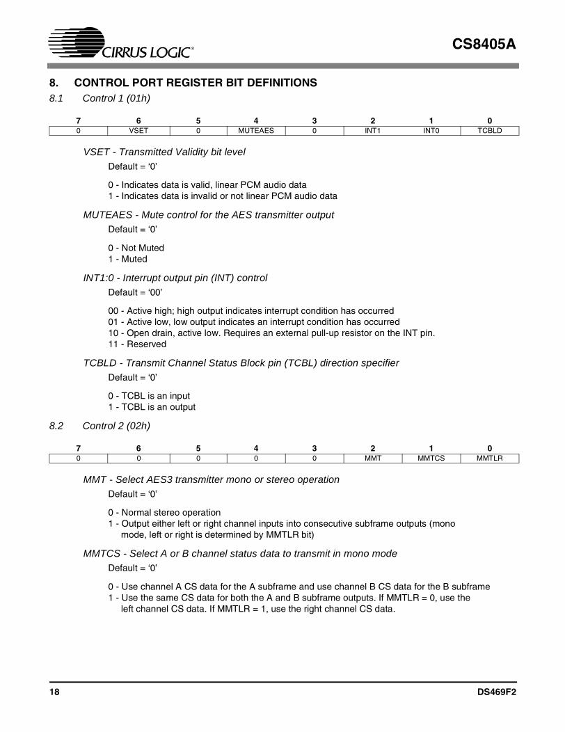
8. CONTROL PORT REGISTER BIT DEFINITIONS8.1 Control 1 (01h)
VSET - Transmitted Validity bit levelDefault = ‘0’
0 - Indicates data is valid, linear PCM audio data1 - Indicates data is invalid or not linear PCM audio data
MUTEAES - Mute control for the AES transmitter outputDefault = ‘0’
0 - Not Muted1 - Muted
INT1:0 - Interrupt output pin (INT) controlDefault = ‘00’
00 - Active high; high output indicates interrupt condition has occurred01 - Active low, low output indicates an interrupt condition has occurred10 - Open drain, active low. Requires an external pull-up resistor on the INT pin.11 - Reserved
TCBLD - Transmit Channel Status Block pin (TCBL) direction specifierDefault = ‘0’
0 - TCBL is an input1 - TCBL is an output
8.2 Control 2 (02h)
MMT - Select AES3 transmitter mono or stereo operationDefault = ‘0’
0 - Normal stereo operation1 - Output either left or right channel inputs into consecutive subframe outputs (mono mode, left or right is determined by MMTLR bit)
MMTCS - Select A or B channel status data to transmit in mono modeDefault = ‘0’
0 - Use channel A CS data for the A subframe and use channel B CS data for the B subframe1 - Use the same CS data for both the A and B subframe outputs. If MMTLR = 0, use the left channel CS data. If MMTLR = 1, use the right channel CS data.
7 6 5 4 3 2 1 00 VSET 0 MUTEAES 0 INT1 INT0 TCBLD
7 6 5 4 3 2 1 00 0 0 0 0 MMT MMTCS MMTLR
18 DS469F2
CS8405A
MMTLR - Channel Selection for AES Transmitter mono modeDefault = ‘0’
0 - Use left channel input data for consecutive subframe outputs1- Use right channel input data for consecutive subframe outputs
8.3 Data Flow Control (03h)
The Data Flow Control register configures the flow of audio data. The output data should be muted prior to changing bits in this register to avoid transients.
TXOFF - AES3 Transmitter Output Driver ControlDefault = ‘0
0 - AES3 transmitter output pin drivers normal operation 1 - AES3 transmitter output pin drivers drive to 0 V.
AESBP - AES3 bypass mode selectionDefault = ‘0’
0 - Normal operation1 - Connect the AES3 transmitter driver input directly to the RXP pin, which becomes a normal TTL threshold digital input. The OMCK clock must be present for the bypass mode to work.
8.4 Clock Source Control (04h)
This register configures the clock sources of various blocks. In conjunction with the Data Flow Control register, various Receiver/Transmitter/Transceiver modes may be selected.
RUN - Controls the internal clocks, allowing the CS8405A to be placed in a “powered down” lowcurrent consumption, state.
Default = ‘0’
0 - Internal clocks are stopped. Internal state machines are reset. The fully static control port registers are operational, allowing registers to be read or changed. Reading and writing the U and C data buffers is not possible. Power consumption is low.1 - Normal part operation. This bit must be set to 1 to allow the CS8405A to begin operation. All input clocks should be stable in frequency and phase when RUN is set to 1.
CLK1:0 - Output master clock (OMCK) input frequency to output sample rate (Fs) ratio selector.If these bits are changed during normal operation, then always stop the CS8405A first (RUN = 0),write the new value, then start the CS8405A (RUN = 1).
Default = ‘00’
00 - OMCK frequency is 256*Fs01 - OMCK frequency is 384*Fs10 - OMCK frequency is 512*Fs11 - Reserved
7 6 5 4 3 2 1 00 TXOFF AESBP 0 0 0 0 0
7 6 5 4 3 2 1 00 RUN CLK1 CLK0 0 0 0 0
DS469F2 19

CS8405A
8.5 Serial Audio Input Port Data Format (05h)
SIMS - Master/Slave Mode SelectorDefault = ‘0’
0 - Serial audio input port is in slave mode1 - Serial audio input port is in master mode
SISF - ISCLK frequency (for master mode)Default = ‘0’
0 - 64*Fs 1 - 128*Fs
SIRES1:0 - Resolution of the input data, for right-justified formatsDefault = ‘00’
00 - 24-bit resolution01 - 20-bit resolution10 - 16-bit resolution11 - Reserved
SIJUST - Justification of SDIN data relative to ILRCKDefault = ‘0’
0 - Left-justified 1 - Right-justified
SIDEL - Delay of SDIN data relative to ILRCK, for left-justified data formatsDefault = ‘0’
0 - MSB of SDIN data occurs in the first ISCLK period after the ILRCK edge (left justified mode)1 - MSB of SDIN data occurs in the second ISCLK period after the ILRCK edge (I²S mode)
SISPOL - ISCLK clock polarityDefault = ‘0’
0 - SDIN sampled on rising edges of ISCLK1 - SDIN sampled on falling edges of ISCLK
SILRPOL - ILRCK clock polarityDefault = ‘0’
0 - SDIN data is for the left channel when ILRCK is high1 - SDIN data is for the right channel when ILRCK is high
7 6 5 4 3 2 1 0SIMS SISF SIRES1 SIRES0 SIJUST SIDEL SISPOL SILRPOL
20 DS469F2

CS8405A
8.6 Interrupt 1 Status (07h) (Read Only)
For all bits in this register, a “1” means the associated interrupt condition has occurred at least once since the register was last read. A ”0” means the associated interrupt condition has NOT occurred since the last reading of the register. Reading the register resets all bits to 0, unless the interrupt mode is set to level and the interrupt source is still true. Status bits that are masked off in the associated mask register will always be “0” in this register. This register defaults to 00h.
TSLIP - AES3 transmitter source data slip interrupt In data flows where OMCK, which clocks the AES3 transmitter, is asynchronous to the data source, this bit will go high every time a data sample is dropped or repeated. When TCBL is an input, this bit will go high on receipt of a new TCBL signal.
EFTC - E to F C-buffer transfer interrupt. The source for this bit is true during the E to F buffer transfer in the C bit buffer management process.
8.7 Interrupt 2 Status (08h) (Read Only)
For all bits in this register, a “1” means the associated interrupt condition has occurred at least once since the register was last read. A ”0” means the associated interrupt condition has NOT occurred since the last reading of the register. Reading the register resets all bits to 0, unless the interrupt mode is set to level and the interrupt source is still true. Status bits that are masked off in the associated mask register will always be “0” in this register. This register defaults to 00h.
EFTU - E to F U-buffer transfer interrupt. (Block Mode only)The source of this bit is true during the E to F buffer transfer in the U bit buffer management process.
8.8 Interrupt 1 Mask (09h)
The bits of this register serve as a mask for the Interrupt 1 register. If a mask bit is set to 1, the error is unmasked, meaning that its occurrence will affect the INT pin and the status register. If a mask bit is set to 0, the error is masked, meaning that its occurrence will not affect the INT pin or the status register. The bit positions align with the corresponding bits in Interrupt 1 register. This register defaults to 00h.
7 6 5 4 3 2 1 0TSLIP 0 0 0 0 0 EFTC 0
7 6 5 4 3 2 1 00 0 0 0 0 EFTU 0 0
7 6 5 4 3 2 1 0TSLIPM 0 0 0 0 0 EFTCM 0
DS469F2 21
CS8405A
8.9 Interrupt 1 Mode MSB (0Ah) and Interrupt 1 Mode LSB (0Bh)
The two Interrupt Mode registers form a 2-bit code for each Interrupt Register 1 function. There are three ways to set the INT pin active in accordance with the interrupt condition. In the Rising edge ac-tive mode, the INT pin becomes active on the arrival of the interrupt condition. In the Falling edge ac-tive mode, the INT pin becomes active on the removal of the interrupt condition. In Level active mode, the INT interrupt pin becomes active during the interrupt condition. Be aware that the active level (Ac-tice High or Low) only depends on the INT[1:0] bits. These registers default to 00.
00 - Rising edge active01 - Falling edge active10 - Level active11 - Reserved
8.10 Interrupt 2 Mask (0Ch)
The bits of this register serve as a mask for the Interrupt 2 register. If a mask bit is set to 1, the error is unmasked, meaning that its occurrence will affect the INT pin and the status register. If a mask bit is set to 0, the error is masked, meaning that its occurrence will not affect the INT pin or the status register. The bit positions align with the corresponding bits in Interrupt 2 register. This register defaults to 00h.
8.11 Interrupt 2 Mode MSB (0Dh) and Interrupt Mode 2 LSB (0Eh)
The two Interrupt Mode registers form a 2-bit code for each Interrupt Register 1 function. There are three ways to set the INT pin active in accordance with the interrupt condition. In the Rising edge ac-tive mode, the INT pin becomes active on the arrival of the interrupt condition. In the Falling edge ac-tive mode, the INT pin becomes active on the removal of the interrupt condition. In Level active mode, the INT interrupt pin becomes active during the interrupt condition. Be aware that the active level (Ac-tive High or Low) only depends on the INT[1:0] bits. These registers default to 00.
00 - Rising edge active01 - Falling edge active10 - Level active11 - Reserved
7 6 5 4 3 2 1 0TSLIP1 0 0 0 0 0 EFTC1 0TSLIP0 0 0 0 0 0 EFTC0 0
7 6 5 4 3 2 1 00 0 0 0 0 EFTUM 0 0
7 6 5 4 3 2 1 00 0 0 0 0 EFTU1 0 00 0 0 0 0 EFTU0 0 0
22 DS469F2
CS8405A
8.12 Channel Status Data Buffer Control (12h)
BSEL - Selects the data buffer register addresses to contain User data or Channel Status dataDefault = ‘0’
0 - Data buffer address space contains Channel Status data1 - Data buffer address space contains User data
Note: There are separate complete buffers for the Channel Status and User bits. This control bit determines which buffer appears in the address space.
EFTCI - E to F C-data buffer transfer inhibit bit. Default = ‘0’
0 - Allow C-data E to F buffer transfers1 - Inhibit C-data E to F buffer transfers
CAM - C-data buffer control port access mode bitDefault = ‘0’
0 - One byte mode1 - Two byte mode
8.13 User Data Buffer Control (13h)
UD - User bit data source specifierDefault = ‘0’
0 - The U pin is an input. The User bit data is latched in on both rising and falling edges of OLRCK. This setting also chooses the U pin as the source for transmitted U data.1 - Sets the U data buffer as the source of transmitted U data. The U pin also becomes an indeterminate output.
UBM1:0 - Sets the operating mode of the AES3 User bit managerDefault = ‘00’
00 - Transmit all zeros mode01 - Block mode10 - Reserved11 - Reserved
EFTUI - E to F U-data buffer transfer inhibit bit (valid in block mode only). Default = ‘0’
0 - Allow U-data E to F buffer transfers1 - Inhibit U-data E to F buffer transfer
7 6 5 4 3 2 1 00 0 BSEL 0 0 EFTCI CAM 0
7 6 5 4 3 2 1 00 0 0 UD UBM1 UBM0 0 EFTUI
DS469F2 23
CS8405A
8.14 Channel Status bit or User bit Data Buffer (20h - 37h)
Either the channel status data buffer E or the separate user bit data buffer E (provided UBM bits are set to block mode) is accessible through these register addresses.
8.15 CS8405A I.D. and Version Register (7Fh) (Read Only)
ID3:0 - ID code for the CS8405A. Permanently set to 0110
VER3:0 - CS8405A revision level. Revision A is coded as 0001
7 6 5 4 3 2 1 0ID3 ID2 ID1 ID0 VER3 VER2 VER1 VER0
24 DS469F2

CS8405A
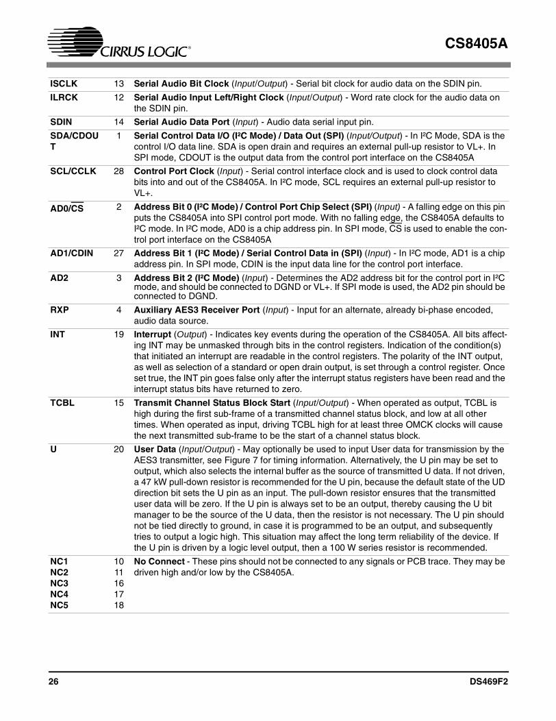
9. PIN DESCRIPTION - SOFTWARE MODE
SDA / CDOUT SCL / CCLK
AD0 / CS AD1 / CDIN
AD2 TXP
RXP TXN
DGND2 H/S
VD+ VL+
DGND4 DGND
DGND3 OMCK
RST U
NC1 INT
NC2 NC5
ILRCK NC4
ISCLK NC3
SDIN TCBL
1
2
3
4
5
6
7
8 21
22
23
24
25
26
27
28
9
10
11
12 17
18
19
20
13
14 15
16
VD+ 6 Digital Power (Input) - Digital core power supply. Typically +5.0 V.
VL+ 23 Logic Power (Input) - Input/Output power supply. Typically +3.3 V or +5.0 V.
DGNDDGND2DGND3DGND4
22587
Ground (Input) - Ground for I/O and core logic.
RST 9 Reset (Input) - When RST is low, the CS8405A enters a low power mode and all internal states are reset. On initial power up, RST must be held low until the power supply is stable, and all input clocks are stable in frequency and phase. This is particularly true in hardware mode with multiple CS8405A devices, where synchronization between devices is important.
H/S 24 Hardware/Software Control Mode Select (Input) -Determines the method of controlling the operation of the CS8405A, and the method of accessing Channel Status and User bit data. In software mode, device control and CS and U data access is primarily through the control port, using a microcontroller. Hardware mode provides an alternate mode of operation, and access to CS and U data is provided by dedicated pins. This pin should be permanently tied to VL+ or DGND.
TXNTXP
2526
Differential Line Drivers (Output) - These pins transmit biphase encoded data. The drivers are pulled low while the CS8405A is in the reset state.
OMCK 21 Master Clock (Input) - The frequency must be 256x, 384x, or 512x the sample rate.
DS469F2 25
CS8405A
ISCLK 13 Serial Audio Bit Clock (Input/Output) - Serial bit clock for audio data on the SDIN pin.
ILRCK 12 Serial Audio Input Left/Right Clock (Input/Output) - Word rate clock for the audio data on the SDIN pin.
SDIN 14 Serial Audio Data Port (Input) - Audio data serial input pin.
SDA/CDOUT
1 Serial Control Data I/O (I²C Mode) / Data Out (SPI) (Input/Output) - In I²C Mode, SDA is the control I/O data line. SDA is open drain and requires an external pull-up resistor to VL+. In SPI mode, CDOUT is the output data from the control port interface on the CS8405A
SCL/CCLK 28 Control Port Clock (Input) - Serial control interface clock and is used to clock control data bits into and out of the CS8405A. In I²C mode, SCL requires an external pull-up resistor to VL+.
AD0/CS 2 Address Bit 0 (I²C Mode) / Control Port Chip Select (SPI) (Input) - A falling edge on this pin puts the CS8405A into SPI control port mode. With no falling edge, the CS8405A defaults to I²C mode. In I²C mode, AD0 is a chip address pin. In SPI mode, CS is used to enable the con-trol port interface on the CS8405A
AD1/CDIN 27 Address Bit 1 (I²C Mode) / Serial Control Data in (SPI) (Input) - In I²C mode, AD1 is a chip address pin. In SPI mode, CDIN is the input data line for the control port interface.
AD2 3 Address Bit 2 (I²C Mode) (Input) - Determines the AD2 address bit for the control port in I²C mode, and should be connected to DGND or VL+. If SPI mode is used, the AD2 pin should be connected to DGND.
RXP 4 Auxiliary AES3 Receiver Port (Input) - Input for an alternate, already bi-phase encoded, audio data source.
INT 19 Interrupt (Output) - Indicates key events during the operation of the CS8405A. All bits affect-ing INT may be unmasked through bits in the control registers. Indication of the condition(s) that initiated an interrupt are readable in the control registers. The polarity of the INT output, as well as selection of a standard or open drain output, is set through a control register. Once set true, the INT pin goes false only after the interrupt status registers have been read and the interrupt status bits have returned to zero.
TCBL 15 Transmit Channel Status Block Start (Input/Output) - When operated as output, TCBL is high during the first sub-frame of a transmitted channel status block, and low at all other times. When operated as input, driving TCBL high for at least three OMCK clocks will cause the next transmitted sub-frame to be the start of a channel status block.
U 20 User Data (Input/Output) - May optionally be used to input User data for transmission by the AES3 transmitter, see Figure 7 for timing information. Alternatively, the U pin may be set to output, which also selects the internal buffer as the source of transmitted U data. If not driven, a 47 kW pull-down resistor is recommended for the U pin, because the default state of the UD direction bit sets the U pin as an input. The pull-down resistor ensures that the transmitted user data will be zero. If the U pin is always set to be an output, thereby causing the U bit manager to be the source of the U data, then the resistor is not necessary. The U pin should not be tied directly to ground, in case it is programmed to be an output, and subsequently tries to output a logic high. This situation may affect the long term reliability of the device. If the U pin is driven by a logic level output, then a 100 W series resistor is recommended.
NC1NC2NC3NC4NC5
1011161718
No Connect - These pins should not be connected to any signals or PCB trace. They may be driven high and/or low by the CS8405A.
26 DS469F2
CS8405A
10.HARDWARE MODEThe CS8405A has a hardware mode that allowsthe use of the device without a microcontroller.Hardware mode is selected by connecting the H/Spin to VL+. The flexibility of the CS8405A is neces-sarily limited in hardware mode. Various pinschange function as described in the hardwaremode pin description section.
The hardware mode data flow is shown inFigure 10. Audio data is input through the serialaudio input port and routed to the AES3 transmit-ter.
10.1 Channel Status, User and Validity Data
The transmitted channel status, user and validitydata can be input in two methods, determined bythe state of the CEN pin. Mode A is selected whenthe CEN pin is low. In mode A, the user bit data andthe validity bit are input through the U and V pins,clocked by both edges of ILRCK. The channel sta-tus data is derived from the state of the COPY/C,ORIG, EMPH, and AUDIO pins. Table 2 showshow the COPY/C and ORIG pins map to channelstatus bits. In consumer mode, the transmitted cat-egory code is set to Sample Rate Converter(0101100).
Mode B is selected when the CEN pin is high. Inmode B, the channel status, user data bits and thevalidity bit are input serially through the COPY/C,U and V pins. Data is clocked into these pins atboth edges of ILRCK. Figure 7 shows the timingrequirements.
The channel status block pin (TCBL) may be an in-put or an output, determined by the state of theTCBLD pin.
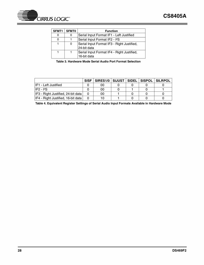
10.2 Serial Audio Port FormatsThe serial audio input port data format is selectedas shown in Table 3, and may be set to master orslave by the state of the APMS input pin. Table 4describes the equivalent software mode, bit settingsfor each of the available formats. Timing diagramsare shown in Figure 6.
AES3Encoder& Tx
SerialAudioInput
C, U, V Data Buffer
ILRCK
ISCLKTXP
COPY/C ORIG EMPH AUDIO TCBL
VL+
H/S
OutputClockSource
OMCK
Power supply pins and the reset pin are omitted from this diagram.Please refer to the Typical Connection Diagram for hook-up details.
SDIN
SFMT1 SFMT0
TXN
CENUV
TCBLDAPMS
Figure 10. Hardware Mode
COPY/C ORIG Function0 0 PRO=0, COPY=0, L=0 copyright0 1 PRO=0, COPY=0, L=1 copyright,
pre-recorded1 0 PRO=0, COPY=1, L=0
non-copyright1 1 PRO=1
Table 2. Hardware Mode COPY/C and ORIG pin functions
DS469F2 27
CS8405A
SFMT1 SFMT0 Function0 0 Serial Input Format IF1 - Left Justified0 1 Serial Input Format IF2 - I²S1 0 Serial Input Format IF3 - Right Justified,
24-bit data1 1 Serial Input Format IF4 - Right Justified,
16-bit data
Table 3. Hardware Mode Serial Audio Port Format Selection
SISF SIRES1/0 SIJUST SIDEL SISPOL SILRPOLIF1 - Left Justified 0 00 0 0 0 0IF2 - I²S 0 00 0 1 0 1IF3 - Right Justified, 24-bit data 0 00 1 0 0 0IF4 - Right Justified, 16-bit data 0 10 1 0 0 0
Table 4. Equivalent Register Settings of Serial Audio Input Formats Available in Hardware Mode
28 DS469F2
CS8405A
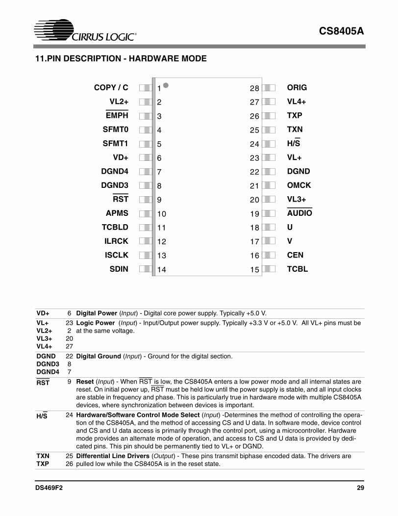
11.PIN DESCRIPTION - HARDWARE MODE
COPY / C ORIG
VL2+ VL4+
EMPH TXP
SFMT0 TXN
SFMT1 H/S
VD+ VL+
DGND4 DGND
DGND3 OMCK
RST VL3+
APMS AUDIO
TCBLD U
ILRCK V
ISCLK CEN
SDIN TCBL
1
2
3
4
5
6
7
8 21
22
23
24
25
26
27
28
9
10
11
12 17
18
19
20
13
14 15
16
VD+ 6 Digital Power (Input) - Digital core power supply. Typically +5.0 V.
VL+VL2+VL3+VL4+
2322027
Logic Power (Input) - Input/Output power supply. Typically +3.3 V or +5.0 V. All VL+ pins must be at the same voltage.
DGNDDGND3DGND4
2287
Digital Ground (Input) - Ground for the digital section.
RST 9 Reset (Input) - When RST is low, the CS8405A enters a low power mode and all internal states are reset. On initial power up, RST must be held low until the power supply is stable, and all input clocks are stable in frequency and phase. This is particularly true in hardware mode with multiple CS8405A devices, where synchronization between devices is important.
H/S 24 Hardware/Software Control Mode Select (Input) -Determines the method of controlling the opera-tion of the CS8405A, and the method of accessing CS and U data. In software mode, device control and CS and U data access is primarily through the control port, using a microcontroller. Hardware mode provides an alternate mode of operation, and access to CS and U data is provided by dedi-cated pins. This pin should be permanently tied to VL+ or DGND.
TXNTXP
2526
Differential Line Drivers (Output) - These pins transmit biphase encoded data. The drivers are pulled low while the CS8405A is in the reset state.
DS469F2 29

CS8405A
OMCK 21 Master Clock (Input) - The frequency must be only 256x the sample rate.
ISCLK 13 Serial Audio Bit Clock (Input/Output) - Serial bit clock for audio data on the SDIN pin.
ILRCK 12 Serial Audio Input Left/Right Clock (Input/Output) - Word rate clock for the audio data on the SDIN pin.
SDIN 14 Serial Audio Data Port (Input) - Audio data serial input pin.
SFMT0 SFMT1
45
Serial Audio Data Format Select (Input) - Selecta the serial audio input port format. See Table 3.
APMS 10 Serial Audio Data Port Master/Slave Select (Input) - APMS should be connected to VL+ to set serial audio input port as a master or connected to DGND to set the port as a slave.
TCBLD 11 Transmit Channel Status Block Direction (Input) - Connect TCBLD to VL+ to set TCBL as an out-put. Connect TCBLD to DGND to set TCBL as an input.
TCBL 15 Transmit Channel Status Block Start (Input/Output) - When operated as output, TCBL is high dur-ing the first sub-frame of a transmitted channel status block, and low at all other times. When oper-ated as input, driving TCBL high for at least three OMCK clocks will cause the next transmitted sub-frame to be the start of a channel status block.
CEN 16 C Bit Enable (Input) - Determines how the channel status data bits are input. When CEN is low, hardware mode A is selected, where the COPY/C, ORIG, EMPH and AUDIO pins are used to enter selected channel status data. When CEN is high, hardware mode B is selected, where the COPY/C pin is used to enter serial channel status data.
V 17 Validity Bit (Input) - In hardware modes A and B, the V pin input determines the state of the validity bit in the outgoing AES3 transmitted data. This pin is sampled on both edges of the ILRCK.
U 18 User Data Bit (Input) - In hardware modes A and B, the U pin input determines the state of the user data bit in the outgoing AES3 transmitted data. This pin is sampled on both edges of the ILRCK.
COPY/C 1 COPY Channel Status Bit/C Bit (Input) - In hardware mode A (CEN = 0), the COPY/C and ORIG pins determine the state of the Copyright, Pro, and L Channel Status bits in the outgoing AES3 data stream, see Table 2. In hardware mode B, the COPY/C pin becomes the direct C bit input data pin.
EMPH 3 Pre-Emphasis Indicator (Input) - In hardware mode A (CEN = 0), the EMPH pin low sets the 3 emphasis channel status bits to indicate 50/15 ms pre-emphasis of the transmitted audio data. If EMPH is high, then the three EMPH channel status bits are set to 000, indicating no pre-emphasis.
AUDIO 19 Audio Channel Status Bit (Input) - In hardware mode A (CEN = 0), the AUDIO pin determines the state of the audio/non audio Channel Status bit in the outgoing AES3 data stream.
ORIG 28 ORIG Channel Status Bit Control (Input) - In hardware mode A (CEN = 0), the ORIG and COPY/C pins determine the state of the Copyright, Pro, and L Channel Status bits in the outgoing AES3 data stream, see Table 2.
30 DS469F2
CS8405A
12.APPLICATIONS
12.1 Reset, Power Down and Start-up When RST is low, the CS8405A enters a low pow-er mode and all internal states are reset, includingthe control port and registers, and the outputs aredisabled. When RST is high, the control port be-comes operational and the desired settings shouldbe loaded into the control registers. Writing a 1 tothe RUN bit will then cause the part to leave the lowpower state and begin operation.
12.2 ID Code and Revision CodeThe CS8405A has a register that contains a four-bit code to indicate that the addressed device is aCS8405A. This is useful when other CS84XX fam-ily members are resident in the same or similarsystems, allowing common software modules.
The CS8405A four-bit revision level code is alsoavailable. This allows the software driver for theCS8405A to identify which revision of the device isin a particular system, and modify its behavior ac-cordingly. To allow for future revisions, it is stronglyrecommended that the revision code is read into avariable area within the microcontroller, and usedwherever appropriate as revision details becomeknown.
12.3 Power Supply, Grounding, and PCB layout
For most applications, the CS8405 can be operat-ed from a single +5.0 V supply, following normal
supply decoupling practices, see Figure 5. “Rec-ommended Connection Diagram for SoftwareMode” on page 10. Note that the I²C protocol issupported only in VL+ = 5.0 V mode. The VL+ sup-plies should be decoupled with a 0.1 µF capacitorto DGND to minimize AES3 transmitter inducedtransients.
Extensive use of power and ground planes, groundplane fill in unused areas and surface mount de-coupling capacitors are recommended. Decou-pling capacitors should be mounted on the sameside of the board as the CS8405A to minimize in-ductance effects, and all decoupling capacitorsshould be as close to the CS8405A as possible.
12.4 Synchronization of Multiple CS8405As
The AES3 transmitters of multiple CS8405As canbe synchronized if all devices share the same mas-ter clock, TCBL, and RST signals and all exit thereset state on the same master clock falling edge.The TCBL pin is used to synchronize multipleCS8405A AES3 transmitters at the channel statusblock boundaries. One CS8405A must have itsTCBL set to master; the others must be set to slaveTCBL. Alternatively, TCBL can be derived from ex-ternal logic, whereby all CS8405A devices shouldbe set to slave TCBL.
DS469F2 31
CS8405A
13. PACKAGE DIMENSIONS
INCHES MILLIMETERSDIM MIN NOM MAX MIN NOM MAX
A 0.093 0.098 0.104 2.35 2.50 2.65A1 0.004 0.008 0.012 0.10 0.20 0.30b 0.013 0.017 0.020 0.33 0.42 0.51C 0.009 0.011 0.013 0.23 0.28 0.32D 0.697 0.705 0.713 17.70 17.90 18.10E 0.291 0.295 0.299 7.40 7.50 7.60e 0.040 0.050 0.060 1.02 1.27 1.52H 0.394 0.407 0.419 10.00 10.34 10.65L 0.016 0.026 0.050 0.40 0.65 1.27∝ 0° 4° 8° 0° 4° 8°
JEDEC #: MS-013
Controlling Dimension is Millimeters
28L SOIC (300 MIL BODY) PACKAGE DRAWING
D
HE
b
A1
A
c
L
∝
SEATINGPLANE
1
e
32 DS469F2
CS8405A
Notes: 1.“D” and “E1” are reference datums and do not included mold flash or protrusions, but do include mold mismatch and are measured at the parting line, mold flash or protrusions shall not exceed 0.20 mm per side.
2.Dimension “b” does not include dambar protrusion/intrusion. Allowable dambar protrusion shall be 0.13 mm total in excess of “b” dimension at maximum material condition. Dambar intrusion shall not reduce dimension “b” by more than 0.07 mm at least material condition.
3.These dimensions apply to the flat section of the lead between 0.10 and 0.25 mm from lead tips.
INCHES MILLIMETERS NOTEDIM MIN NOM MAX MIN NOM MAX
A -- -- 0.47 -- -- 1.20A1 0.002 0.004 0.006 0.05 0.10 0.15A2 0.03150 0.035 0.04 0.80 0.90 1.00b 0.00748 0.0096 0.012 0.19 0.245 0.30 2,3D 0.378 BSC 0.382 BSC 0.386 BSC 9.60 BSC 9.70 BSC 9.80 BSC 1E 0.248 0.2519 0.256 6.30 6.40 6.50
E1 0.169 0.1732 0.177 4.30 4.40 4.50 1e -- 0.026 BSC -- -- 0.65 BSC --L 0.020 0.024 0.029 0.50 0.60 0.75∝ 0° 4° 8° 0° 4° 8°
JEDEC #: MO-153Controlling Dimension is Millimeters.
28L TSSOP (4.4 mm BODY) PACKAGE DRAWING
E
N
1 2 3
e b2 A1
A2 A
D
SEATINGPLANE
E11
L
SIDE VIEW
END VIEW
TOP VIEW
∝
DS469F2 33
CS8405A
14. APPENDIX A: EXTERNAL AES3/SPDIF/IEC60958 TRANSMITTER AND RECEIVER COMPONENTS
This section details the external components re-quired to interface the AES3 transmitter and re-ceiver to cables and fiber-optic components.
14.1 AES3 Transmitter External Components
The output drivers on the CS8405A are designedto drive both the professional and consumer inter-faces. The AES3 specification for profession-al/broadcast use calls for a 110 Ω sourceimpedance and a balanced drive capability. Sincethe transmitter output impedance is very low, a110 Ω resistor should be placed in series with oneof the transmit pins. The specifications call for abalanced output drive of 2-7 V peak-to-peak into a110 Ω load with no cable attached. Using the cir-cuit in Figure 11, the output of the transformer isshort-circuit protected, has the proper source im-pedance, and provides a 5 V peak-to-peak signalinto a 110 Ω load. Lastly, the two output pinsshould be attached to an XLR connector with malepins and a female shell, and with pin 1 of the con-nector grounded.
In the case of consumer use, the IEC60958 speci-fications call for an unbalanced drive circuit with anoutput impedance of 75 Ω and a output drive levelof 0.5 V peak-to-peak ±20% when measuredacross a 75 Ω load using no cable. The circuitshown in Figure 12 only uses the TXP pin and pro-vides the proper output impedance and drive levelusing standard 1% resistors. If VL+ is driven from+3.3 V, use resistor values of 243 Ω and 107 Ω.The connector for a consumer application wouldbe an RCA phono socket. This circuit is also shortcircuit protected.
The TXP pin may be used to drive TTL or CMOSgates as shown in Figure 13. This circuit may beused for optical connectors for digital audio sincethey usually have TTL or CMOS compatible inputs.This circuit is also useful when driving multiple dig-ital audio outputs since RS422 line drivers haveTTL compatible inputs.
14.2 Isolating Transformer RequirementsPlease refer to the application note AN134: AESand SPDIF Recommended Transformers for re-sources on transformer selection.
110-(RTXP+RTXN)
TXP
TXN
XLR
1
CS8405A
Figure 11. Professional Output Circuit Figure 12. Consumer Output Circuit
3 7 4 -R T X P
9 0 .9 Ω
T X P
T X N
C S 8 4 0 5 A
Figure 13. TTL/CMOS Output Circuit
TXP
TXN
TTL orCMOS Gate
CS8405A
34 DS469F2

CS8405A
15.APPENDIX B: CHANNEL STATUS AND USER DATA BUFFER MANAGEMENT
The CS8405A has a comprehensive channel sta-tus (C) and user (U) data buffering scheme whichallows the user to manage the C and U datathrough the control port.
15.1 AES3 Channel Status(C) Bit Management
The CS8405A contains sufficient RAM to store afull block of C data for both A and B channels(192x2 = 384 bits), and also 384 bits of U informa-tion. The user may read from or write to these RAMbuffers through the control port.
The CS8405A manages the flow of channel statusdata at the block level, meaning that entire blocksof channel status information are buffered at the in-put, synchronized to the output timebase, and thentransmitted. The buffering scheme involves a cas-cade of 2 block-sized buffers, named E and F, asshown in Figure 14. The MSB of each byte repre-sents the first bit in the serial C data stream. Forexample, the MSB of byte 0 (which is at control portaddress 20h) is the consumer/professional bit forchannel status block A.
The E buffer is accessible from the control port, al-lowing read and writing of the C data. The F bufferis used as the source of C data for the AES3 trans-mitter. The F buffer accepts block transfers fromthe E buffer.
15.1.1 Accessing the E bufferThe user can monitor the data being transferred byreading the E buffer, which is mapped into the reg-ister space of the CS8405A, through the controlport. The user can modify the data to be transmit-ted by writing to the E buffer.
The user can configure the interrupt enable regis-ter to cause interrupts to occur whenever “E to F”buffer transfers occur. This allows determination ofthe allowable time periods to interact with the Ebuffer.
Also provided is an “E to F” inhibit bit. The “E to F”buffer transfer is disabled whenever the user setsthis bit. This may be used whenever “long” controlport interactions are occurring.
A flowchart for reading and writing to the E bufferis shown in Figure 15. For writing, the sequencestarts after a E to F transfer, which is based on theoutput timebase.
If the channel status block to transmit indicatesPRO mode, then the CRCC byte is automaticallycalculated by the CS8405A, and does not have tobe written into the last byte of the block by the hostmicrocontroller. This is also true if the channel sta-tus data is entered serially through the COPY/C pinwhen the part is in hardware mode.
Contro l Port
ToAES3Transm itter
E
24words
8-bits 8-b itsA B
F
Transm itDataBuffer
Figure 14. Channel Status Data Buffer Structure
E to F interrupt occurs
Optionally set E to F inhibit
If set, clear E to F inhibit
Return
Write E data
Wait for E to F transfer
Figure 15. Flowchart for Writing the E Buffer
DS469F2 35
CS8405A
15.1.2 Serial Copy Management System (SCMS)
In software mode, the CS8405A allows read/mod-ify/write access to all the channel status bits. Forconsumer mode SCMS compliance, the host mi-crocontroller needs to manipulate the CategoryCode, Copy bit and L bit appropriately.
In hardware mode, the SCMS protocol can be fol-lowed by either using the COPY and ORIG inputpins, or by using the C bit serial input pin. Theseoptions are documented in the hardware modesection of this data sheet.
15.1.3 Channel Status Data E Buffer Access
The E buffer is organized as 24 x 16-bit words. Foreach word the MS Byte is the A channel data, andthe LS Byte is the B channel data (see Figure 14).
There are two methods of accessing this memory,known as one byte mode and two byte mode. Thedesired mode is selected through a control registerbit.
15.1.3.1 One Byte modeIn many applications, the channel status blocks forthe A and B channels will be identical. In this situ-ation, if the user reads a byte from one of the chan-nel's blocks, the corresponding byte for the otherchannel will be the same. Similarly, if the userwrote a byte to one channel's block, it would benecessary to write the same byte to the otherblock. One byte mode takes advantage of the oftenidentical nature of A and B channel status data.
When reading data in one byte mode, a single byteis returned, which can be from channel A or B data,depending on a register control bit. If a write is be-ing done, the CS8405A expects a single byte to beinput to its control port. This byte will be written toboth the A and B locations in the addressed word.
One byte mode saves the user substantial controlport access time, as it effectively accesses 2 bytesworth of information in 1 byte's worth of accesstime. If the control port's auto increment address-
ing is used in combination with this mode, multi-byte accesses such as full-block reads or writescan be done especially efficiently.
15.1.3.2 Two Byte modeThere are those applications in which the A and Bchannel status blocks will not be the same, and theuser is interested in accessing both blocks. Inthese situations, two byte mode should be used toaccess the E buffer.
In this mode, a read will cause the CS8405A to out-put two bytes from its control port. The first byte outwill represent the A channel status data, and the2nd byte will represent the B channel status data.Writing is similar, in that two bytes must now be in-put to the CS8405A's control port. The A channelstatus data is first, B channel status data second.
15.2 AES3 User (U) Bit ManagementThe CS8405A U bit manager has two operatingmodes:Mode 1. Transmit all zeros.Mode 2. Block mode.
15.2.1 Mode 1: Transmit All ZerosMode 1 causes only zeros to be transmitted in theoutput U data, regardless of E buffer contents. Thismode is intended for the user who wants the outputU channel to contain no data.
15.2.2 Mode 2: Block ModeMode 2 is very similar to the scheme used to controlthe C bits. Entire blocks of U data are buffered using2 block-sized RAMs to perform the buffering. Theuser has access to the first buffer, denoted the E buff-er, through the control port. It is the only mode inwhich the user can merge his own U data into thetransmitted AES3 data stream. The U buffer accessonly operates in two byte mode, since there is no con-cept of A and B blocks for user data. The arrange-ment of the data is as follows:Bit15[A7]Bit14[B7]Bit13[A6]Bit12[B6]...Bit1[A0]Bit0[B0]. The arrangement of the data in each byte isthat the MSB is the first transmitted bit. The bit for theA subframe is followed by the bit for the B subframe.
36 DS469F2

CS8405A
16. REVISION HISTORY
Release Date Changes
PP1 November 1999 1st Preliminary Release
PP2 November 2000 2nd Preliminary Release
PP3 May 2001 3rd Preliminary Release
PP4 June 2002 4th Preliminary Release
PP5 March 2003 5th Preliminary Release
F1 January 2004 Final Release
F2 August 2004 Added lead-free device ordering information.
Table 5. Revision History
Contacting Cirrus Logic SupportFor all product questions and inquiries contact a Cirrus Logic Sales Representative. To find the one nearest to you go to www.cirrus.com
IMPORTANT NOTICE
Cirrus Logic, Inc. and its subsidiaries ("Cirrus") believe that the information contained in this document is accurate and reliable. However, the information is subjectto change without notice and is provided "AS IS" without warranty of any kind (express or implied). Customers are advised to obtain the latest version of relevantinformation to verify, before placing orders, that information being relied on is current and complete. All products are sold subject to the terms and conditions of salesupplied at the time of order acknowledgment, including those pertaining to warranty, patent infringement, and limitation of liability. No responsibility is assumed byCirrus for the use of this information, including use of this information as the basis for manufacture or sale of any items, or for infringement of patents or other rightsof third parties. This document is the property of Cirrus and by furnishing this information, Cirrus grants no license, express or implied under any patents, mask workrights, copyrights, trademarks, trade secrets or other intellectual property rights. Cirrus owns the copyrights associated with the information contained herein andgives consent for copies to be made of the information only for use within your organization with respect to Cirrus integrated circuits or other products of Cirrus. Thisconsent does not extend to other copying such as copying for general distribution, advertising or promotional purposes, or for creating any work for resale.
An export permit needs to be obtained from the competent authorities of the Japanese Government if any of the products or technologies described in this materialand controlled under the "Foreign Exchange and Foreign Trade Law" is to be exported or taken out of Japan. An export license and/or quota needs to be obtainedfrom the competent authorities of the Chinese Government if any of the products or technologies described in this material is subject to the PRC Foreign Trade Lawand is to be exported or taken out of the PRC.
CERTAIN APPLICATIONS USING SEMICONDUCTOR PRODUCTS MAY INVOLVE POTENTIAL RISKS OF DEATH, PERSONAL INJURY, OR SEVERE PROP-ERTY OR ENVIRONMENTAL DAMAGE (“CRITICAL APPLICATIONS”). CIRRUS PRODUCTS ARE NOT DESIGNED, AUTHORIZED OR WARRANTED FOR USEIN AIRCRAFT SYSTEMS, MILITARY APPLICATIONS, PRODUCTS SURGICALLY IMPLANTED INTO THE BODY, LIFE SUPPORT PRODUCTS OR OTHERCRITICAL APPLICATIONS (INCLUDING MEDICAL DEVICES, AIRCRAFT SYSTEMS OR COMPONENTS AND PERSONAL OR AUTOMOTIVE SAFETY OR SE-CURITY DEVICES). INCLUSION OF CIRRUS PRODUCTS IN SUCH APPLICATIONS IS UNDERSTOOD TO BE FULLY AT THE CUSTOMER’S RISK AND CIR-RUS DISCLAIMS AND MAKES NO WARRANTY, EXPRESS, STATUTORY OR IMPLIED, INCLUDING THE IMPLIED WARRANTIES OF MERCHANTABILITY ANDFITNESS FOR PARTICULAR PURPOSE, WITH REGARD TO ANY CIRRUS PRODUCT THAT IS USED IN SUCH A MANNER. IF THE CUSTOMER OR CUS-TOMER’S CUSTOMER USES OR PERMITS THE USE OF CIRRUS PRODUCTS IN CRITICAL APPLICATIONS, CUSTOMER AGREES, BY SUCH USE, TO FUL-LY INDEMNIFY CIRRUS, ITS OFFICERS, DIRECTORS, EMPLOYEES, DISTRIBUTORS AND OTHER AGENTS FROM ANY AND ALL LIABILITY, INCLUDINGATTORNEYS’ FEES AND COSTS, THAT MAY RESULT FROM OR ARISE IN CONNECTION WITH THESE USES.
Cirrus Logic, Cirrus, and the Cirrus Logic logo designs are trademarks of Cirrus Logic, Inc. All other brand and product names in this document may be trademarksor service marks of their respective owners.
I²C is a registered trademark of Philips Semiconductor. Purchase of I²C Components of Cirrus Logic, Inc., or one of its sublicensed Associated Companies conveysa license under the Philips I²C Patent Rights to use those components in a standard I²C system.
DS469F2 37