Embed Size (px)
Citation preview
Output Current (A)
Effic
iency (
%)
Pow
er
Loss (
W)
0 5 10 15 20 2540 0
50 1
60 2
70 3
80 4
90 5
100 6
G029
VGS = 5VVIN = 12VVOUT = 1.3VLOUT = 0.3,HfSW = 500kHzTA = 25C
TGR
VIN
PGND
VSW
TG
BG
S0474-01
ENABLE
ENABLE
PWM
GND
BST
DRVH
LL
DRVL
CSD86350Q5DDriver IC
VDD VI
VO
VDD
ControlFET
SyncFET
PWM
P0116-01
1
2
3 VSW
VSW
VSW
4 BG5TGR
6TG
PGND
(Pin 9)
7VIN
8VIN
Product
Folder
Sample &Buy
Technical
Documents
Tools &
Software
Support &Community
An IMPORTANT NOTICE at the end of this data sheet addresses availability, warranty, changes, use in safety-critical applications,intellectual property matters and other important disclaimers. PRODUCTION DATA.
CSD86350Q5DSLPS223F –MAY 2010–REVISED OCTOBER 2016
CSD86350Q5D Synchronous Buck NexFET™ Power Block
1
1 Features1• Half-Bridge Power Block• 90% System Efficiency at 25 A• Up to 40-A Operation• High-Frequency Operation (up to 1.5 MHz)• High-Density SON 5-mm × 6-mm Footprint• Optimized for 5-V Gate Drive• Low-Switching Losses• Ultra-Low Inductance Package• RoHS Compliant• Halogen Free• Lead-Free Terminal Plating
2 Applications• Synchronous Buck Converters
– High-Frequency Applications– High-Current, Low-Duty Cycle Applications
• Multiphase Synchronous Buck Converters• POL DC-DC Converters• IMVP, VRM, and VRD Applications
3 DescriptionThe CSD86350Q5D NexFET™ power block is anoptimized design for synchronous buck applicationsoffering high-current, high-efficiency, and high-frequency capability in a small 5-mm × 6-mm outline.Optimized for 5-V gate drive applications, this productoffers a flexible solution capable of offering a high-density power supply when paired with any 5-V gatedrive from an external controller/driver.
.
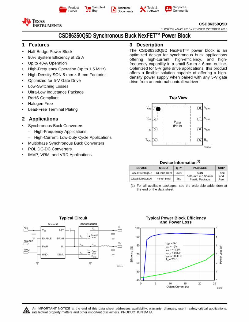
Top View
.
Device Information(1)
DEVICE MEDIA QTY PACKAGE SHIP
CSD86350Q5D 13-Inch Reel 2500 SON5.00-mm × 6.00-mm
Plastic Package
TapeandReelCSD86350Q5DT 7-Inch Reel 250
(1) For all available packages, see the orderable addendum atthe end of the data sheet.
.
.
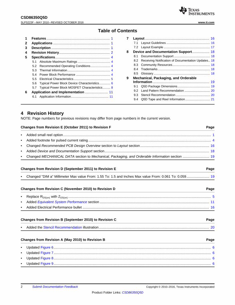
Typical Circuit Typical Power Block Efficiencyand Power Loss
2
CSD86350Q5DSLPS223F –MAY 2010–REVISED OCTOBER 2016 www.ti.com
Product Folder Links: CSD86350Q5D
Submit Documentation Feedback Copyright © 2010–2016, Texas Instruments Incorporated
Table of Contents1 Features .................................................................. 12 Applications ........................................................... 13 Description ............................................................. 14 Revision History..................................................... 25 Specifications......................................................... 4
5.1 Absolute Maximum Ratings ...................................... 45.2 Recommended Operating Conditions....................... 45.3 Thermal Information .................................................. 45.4 Power Block Performance ........................................ 45.5 Electrical Characteristics........................................... 55.6 Typical Power Block Device Characteristics............. 65.7 Typical Power Block MOSFET Characteristics......... 8
6 Application and Implementation ........................ 116.1 Application Information............................................ 11
7 Layout ................................................................... 167.1 Layout Guidelines ................................................... 167.2 Layout Example ...................................................... 17
8 Device and Documentation Support.................. 188.1 Documentation Support .......................................... 188.2 Receiving Notification of Documentation Updates.. 188.3 Community Resources............................................ 188.4 Trademarks ............................................................. 188.5 Glossary .................................................................. 18
9 Mechanical, Packaging, and OrderableInformation ........................................................... 199.1 Q5D Package Dimensions...................................... 199.2 Land Pattern Recommendation .............................. 209.3 Stencil Recommendation ........................................ 209.4 Q5D Tape and Reel Information............................. 21
4 Revision HistoryNOTE: Page numbers for previous revisions may differ from page numbers in the current version.
Changes from Revision E (October 2011) to Revision F Page
• Added small reel option .......................................................................................................................................................... 1• Added footnote for pulsed current rating ................................................................................................................................ 4• Changed Recommended PCB Design Overview section to Layout section ........................................................................ 16• Added Device and Documentation Support section............................................................................................................. 18• Changed MECHANICAL DATA section to Mechanical, Packaging, and Orderable Information section ............................ 19
Changes from Revision D (September 2011) to Revision E Page
• Changed "DIM a" Millimeter Max value From: 1.55 To: 1.5 and Inches Max value From: 0.061 To: 0.059........................ 19
Changes from Revision C (November 2010) to Revision D Page
• Replace RDS(on) with ZDS(on) ..................................................................................................................................................... 5• Added Equivalent System Performance section .................................................................................................................. 11• Added Electrical Performance bullet .................................................................................................................................... 16
Changes from Revision B (September 2010) to Revision C Page
• Added the Stencil Recommendation illustration................................................................................................................... 20
Changes from Revision A (May 2010) to Revision B Page
• Updated Figure 6.................................................................................................................................................................... 6• Updated Figure 7.................................................................................................................................................................... 6• Updated Figure 8.................................................................................................................................................................... 6• Updated Figure 9.................................................................................................................................................................... 6
3
CSD86350Q5Dwww.ti.com SLPS223F –MAY 2010–REVISED OCTOBER 2016
Product Folder Links: CSD86350Q5D
Submit Documentation FeedbackCopyright © 2010–2016, Texas Instruments Incorporated
Changes from Original (May 2010) to Revision A Page
• Changed graph title From: TYPICAL EFFICIENCY vs POWER LOSS To: TYPICAL POWER BLOCK EFFICIENCYand POWER LOSS ................................................................................................................................................................ 1
• Updated the Land Pattern Recommendation illustration...................................................................................................... 20

4
CSD86350Q5DSLPS223F –MAY 2010–REVISED OCTOBER 2016 www.ti.com
Product Folder Links: CSD86350Q5D
Submit Documentation Feedback Copyright © 2010–2016, Texas Instruments Incorporated
(1) Stresses beyond those listed under Absolute Maximum Ratings may cause permanent damage to the device. These are stress ratingsonly, and functional operation of the device at these or any other conditions beyond those indicated in the Recommended OperatingConditions is not implied. Exposure to absolute-maximum-rated conditions for extended periods may affect device reliability.
(2) Pulse duration ≤ 50 µs, duty cycle ≤ 1%.
5 Specifications
5.1 Absolute Maximum RatingsTA = 25°C (unless otherwise noted) (1)
MIN MAX UNIT
VoltageVIN to PGND –0.8 25
VTG to TGR –8 10BG to PGND –8 10
Pulsed current rating, IDM(2) 120 A
Power dissipation, PD 13 W
Avalanche energy, EASSync FET, ID = 100 A, L = 0.1 mH 500
mJControl FET, ID = 58 A, L = 0.1 mH 168
Operating junction, TJ –55 150 °CStorage temperature, TSTG –55 150 °C
5.2 Recommended Operating ConditionsTA = 25° (unless otherwise noted)
MIN MAX UNITVGS Gate drive voltage 4.5 8 VVIN Input supply voltage 22 VfSW Switching frequency CBST = 0.1 μF (min) 200 1500 kHz
Operating current 40 ATJ Operating temperature 125 °C
(1) Device mounted on FR4 material with 1-in2 (6.45-cm2) Cu.(2) RθJC is determined with the device mounted on a 1-in2 (6.45-cm2), 2 oz (0.071-mm) thick Cu pad on a 1.5-in × 1.5-in
(3.81-cm × 3.81-cm), 0.06-in (1.52-mm) thick FR4 board. RθJC is specified by design while RθJA is determined by the user’s boarddesign.
5.3 Thermal InformationTA = 25°C (unless otherwise stated)
THERMAL METRIC MIN TYP MAX UNIT
RθJAJunction-to-ambient thermal resistance (min Cu) (1) (2) 102 °C/WJunction-to-ambient thermal resistance (max Cu) (1) (2) 50 °C/W
RθJCJunction-to-case thermal resistance (top of package) (2) 20 °C/WJunction-to-case thermal resistance (PGND pin) (2) 2 °C/W
(1) Measurement made with six 10-µF (TDK C3216X5R1C106KT or equivalent) ceramic capacitors placed across VIN to PGND pins andusing a high-current 5-V driver IC.
5.4 Power Block PerformanceTA = 25° (unless otherwise noted)
PARAMETER CONDITIONS MIN TYP MAX UNIT
PLOSS Power loss (1)
VIN = 12 V, VGS = 5 V,VOUT = 1.3 V, IOUT = 25 A,fSW = 500 kHz,LOUT = 0.3 µH, TJ = 25°C
2.8 W
IQVIN VIN quiescent current TG to TGR = 0 VBG to PGND = 0 V 10 µA
HD
HG
LG
LD
M0189-01
86350 5x6 QFN TTA MIN Rev1
LS
HS
HD
HG
LG
LD
M0190-01
86350 5x6 QFN TTA MIN Rev1
LS
HS
5
CSD86350Q5Dwww.ti.com SLPS223F –MAY 2010–REVISED OCTOBER 2016
Product Folder Links: CSD86350Q5D
Submit Documentation FeedbackCopyright © 2010–2016, Texas Instruments Incorporated
(1) Specified by design.
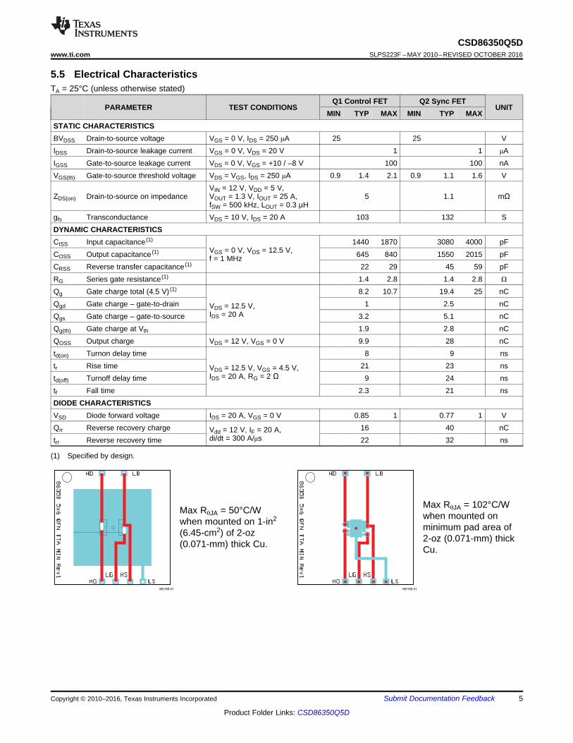
5.5 Electrical CharacteristicsTA = 25°C (unless otherwise stated)
PARAMETER TEST CONDITIONSQ1 Control FET Q2 Sync FET
UNITMIN TYP MAX MIN TYP MAX
STATIC CHARACTERISTICSBVDSS Drain-to-source voltage VGS = 0 V, IDS = 250 μA 25 25 VIDSS Drain-to-source leakage current VGS = 0 V, VDS = 20 V 1 1 μAIGSS Gate-to-source leakage current VDS = 0 V, VGS = +10 / –8 V 100 100 nAVGS(th) Gate-to-source threshold voltage VDS = VGS, IDS = 250 μA 0.9 1.4 2.1 0.9 1.1 1.6 V
ZDS(on) Drain-to-source on impedanceVIN = 12 V, VDD = 5 V,VOUT = 1.3 V, IOUT = 25 A,fSW = 500 kHz, LOUT = 0.3 µH
5 1.1 mΩ
gfs Transconductance VDS = 10 V, IDS = 20 A 103 132 SDYNAMIC CHARACTERISTICSCISS Input capacitance (1)
VGS = 0 V, VDS = 12.5 V,f = 1 MHz
1440 1870 3080 4000 pFCOSS Output capacitance (1) 645 840 1550 2015 pFCRSS Reverse transfer capacitance (1) 22 29 45 59 pFRG Series gate resistance (1) 1.4 2.8 1.4 2.8 Ω
Qg Gate charge total (4.5 V) (1)
VDS = 12.5 V,IDS = 20 A
8.2 10.7 19.4 25 nCQgd Gate charge – gate-to-drain 1 2.5 nCQgs Gate charge – gate-to-source 3.2 5.1 nCQg(th) Gate charge at Vth 1.9 2.8 nCQOSS Output charge VDS = 12 V, VGS = 0 V 9.9 28 nCtd(on) Turnon delay time
VDS = 12.5 V, VGS = 4.5 V,IDS = 20 A, RG = 2 Ω
8 9 nstr Rise time 21 23 nstd(off) Turnoff delay time 9 24 nstf Fall time 2.3 21 nsDIODE CHARACTERISTICSVSD Diode forward voltage IDS = 20 A, VGS = 0 V 0.85 1 0.77 1 VQrr Reverse recovery charge Vdd = 12 V, IF = 20 A,
di/dt = 300 A/μs16 40 nC
trr Reverse recovery time 22 32 ns
Max RθJA = 50°C/Wwhen mounted on 1-in2
(6.45-cm2) of 2-oz(0.071-mm) thick Cu.
Max RθJA = 102°C/Wwhen mounted onminimum pad area of2-oz (0.071-mm) thickCu.
Board Temperature (C)
Outp
ut C
urr
ent (A
)
0 20 40 60 80 100 120 1400
5
10
15
20
25
30
35
40
45
50
5
15
25
35
45
G005
VIN = 12VVGS = 5VVOUT = 1.3V fSW = 500kHzLOUT = 0.3)H
Ambient Temperature (C)
Outp
ut C
urr
ent (A
)
0 10 20 30 40 50 60 70 80 900
5
10
15
20
25
30
35
40
45
50
5
15
25
35
45
G003
VIN = 12VVGS = 5VVOUT = 1.3V fSW = 500kHzLOUT = 0.3*H
400LFM200LFM100LFMNat Conv
Ambient Temperature (C)
Outp
ut C
urr
ent (A
)
0 10 20 30 40 50 60 70 80 900
5
10
15
20
25
30
35
40
45
50
5
15
25
35
45
G004
VIN = 12VVGS = 5VVOUT = 1.3V fSW = 500kHzLOUT = 0.3*H
400LFM200LFM100LFMNat Conv
Output Current (A)
Pow
er
Loss (
W)
0 5 10 15 20 25 30 35 400
1
2
3
4
5
6
7
8
9
10
1
3
5
7
9
G001
VIN = 12VVGS = 5VVOUT = 1.3V fSW = 500kHzLOUT = 0.3*H
Junction Temperature (C)
Pow
er
Loss, N
orm
aliz
ed
50 25 0 25 50 75 100 125 1500.5
0.6
0.7
0.8
0.9
1
1.1
1.2
1
G002
VIN = 12VVGS = 5VVOUT = 1.3V fSW = 500kHzLOUT = 0.31H
6
CSD86350Q5DSLPS223F –MAY 2010–REVISED OCTOBER 2016 www.ti.com
Product Folder Links: CSD86350Q5D
Submit Documentation Feedback Copyright © 2010–2016, Texas Instruments Incorporated
(1) The Typical Power Block System Characteristic curves are based on measurements made on a PCB design with dimensions of 4 in (W)× 3.5 in (L) x 0.062 in (H) and 6 copper layers of 1-oz copper thickness. See Application and Implementation for detailed explanation.
5.6 Typical Power Block Device CharacteristicsTJ = 125°C, unless stated otherwise.
Figure 1. Power Loss vs Output Current Figure 2. Normalized Power Loss vs Temperature
Figure 3. Safe Operating Area – PCB Vertical Mount (1) Figure 4. Safe Operating Area – PCB Horizontal Mount (1)
Figure 5. Typical Safe Operating Area (1)

Output Voltage (V)
Pow
er
Loss, N
orm
aliz
ed
0.5 0.9 1.3 1.7 2.1 2.5 2.9 3.3 3.7 4.1 4.5 4.9 5.30.8
0.9
1
1.1
1.2
1.3
1.4
1.5
1.6
1.7
1.8
$5.2
$2.6
0
2.6
5.2
7.8
10.4
13
15.6
18.2
20.8
G008
VGS = 5VVIN = 12V LOUT = 0.3+HfSW = 500kHzIO = 40A
SO
A T
em
pera
ture
Adj (
C)
! " # $ % "
#
$
%
!
"
&!
&#%
&!
&"
"
!
#%
!
!#
'%
()(('*)!((+,)(-*.)!/ ) 0
*0,012
Switching Frequency (kHz)
Pow
er
Loss, N
orm
aliz
ed
200 350 500 650 800 950 1100 1250 1400 15500.6
0.7
0.8
0.9
1
1.1
1.2
1.3
1.4
1.5
1.6
*10.5
*7.9
*5.2
*2.6
0
2.6
5.2
7.9
10.5
13.1
15.7
G006
VIN = 12VVGS = 5VVOUT = 1.3V LOUT = 0.32HIO = 40A
SO
A T
em
pera
ture
Adj (
C)
Input Voltage (V)
Pow
er
Loss, N
orm
aliz
ed
2 4 6 8 10 12 14 16 18 20 22
0.6
0.7
0.8
0.9
1
1.1
1.2
1.3
1.4
1.5
1.6
%10.5
%7.8
%5.2
%2.6
0
2.6
5.2
7.8
10.5
13.1
15.7
G007
VGS = 5V
VOUT = 1.3V
LOUT = 0.3,HfSW = 500kHz
IO = 40A
SO
A T
em
pera
ture
Adj (
C)
7
CSD86350Q5Dwww.ti.com SLPS223F –MAY 2010–REVISED OCTOBER 2016
Product Folder Links: CSD86350Q5D
Submit Documentation FeedbackCopyright © 2010–2016, Texas Instruments Incorporated
Typical Power Block Device Characteristics (continued)TJ = 125°C, unless stated otherwise.
Figure 6. Normalized Power Loss vs Switching Frequency Figure 7. Normalized Power Loss vs Input Voltage
Figure 8. Normalized Power Loss vs Output Voltage Figure 9. Normalized Power Loss vs Output Inductance
8
CSD86350Q5DSLPS223F –MAY 2010–REVISED OCTOBER 2016 www.ti.com
Product Folder Links: CSD86350Q5D
Submit Documentation Feedback Copyright © 2010–2016, Texas Instruments Incorporated
5.7 Typical Power Block MOSFET CharacteristicsTA = 25°C, unless stated otherwise.
Figure 10. Control MOSFET Saturation Figure 11. Sync MOSFET Saturation
Figure 12. Control MOSFET Transfer Figure 13. Sync MOSFET Transfer
Figure 14. Control MOSFET Gate Charge Figure 15. Sync MOSFET Gate Charge
!
"#$°#
"#$°#
%$&
!
"#$°#
"#$°#
%$&
!"#
!"#$
!"
!"
9
CSD86350Q5Dwww.ti.com SLPS223F –MAY 2010–REVISED OCTOBER 2016
Product Folder Links: CSD86350Q5D
Submit Documentation FeedbackCopyright © 2010–2016, Texas Instruments Incorporated
Typical Power Block MOSFET Characteristics (continued)TA = 25°C, unless stated otherwise.
Figure 16. Control MOSFET Capacitance Figure 17. Sync MOSFET Capacitance
Figure 18. Control MOSFET VGS(th) Figure 19. Sync MOSFET VGS(th)
Figure 20. Control MOSFET RDS(on) vs VGS Figure 21. Sync MOSFET RDS(on) vs VGS
!
!
!
"#$%
&!$ &
!"
#$%&
'!% '
10
CSD86350Q5DSLPS223F –MAY 2010–REVISED OCTOBER 2016 www.ti.com
Product Folder Links: CSD86350Q5D
Submit Documentation Feedback Copyright © 2010–2016, Texas Instruments Incorporated
Typical Power Block MOSFET Characteristics (continued)TA = 25°C, unless stated otherwise.
Figure 22. Control MOSFET Normalized RDS(on) Figure 23. Sync MOSFET Normalized RDS(on)
Figure 24. Control MOSFET Body Diode Figure 25. Sync MOSFET Body Diode
Figure 26. Control MOSFET Unclamped Inductive Switching Figure 27. Sync MOSFET Unclamped Inductive Switching
11
CSD86350Q5Dwww.ti.com SLPS223F –MAY 2010–REVISED OCTOBER 2016
Product Folder Links: CSD86350Q5D
Submit Documentation FeedbackCopyright © 2010–2016, Texas Instruments Incorporated
6 Application and Implementation
NOTEInformation in the following applications sections is not part of the TI componentspecification, and TI does not warrant its accuracy or completeness. TI’s customers areresponsible for determining suitability of components for their purposes. Customers shouldvalidate and test their design implementation to confirm system functionality.
6.1 Application Information
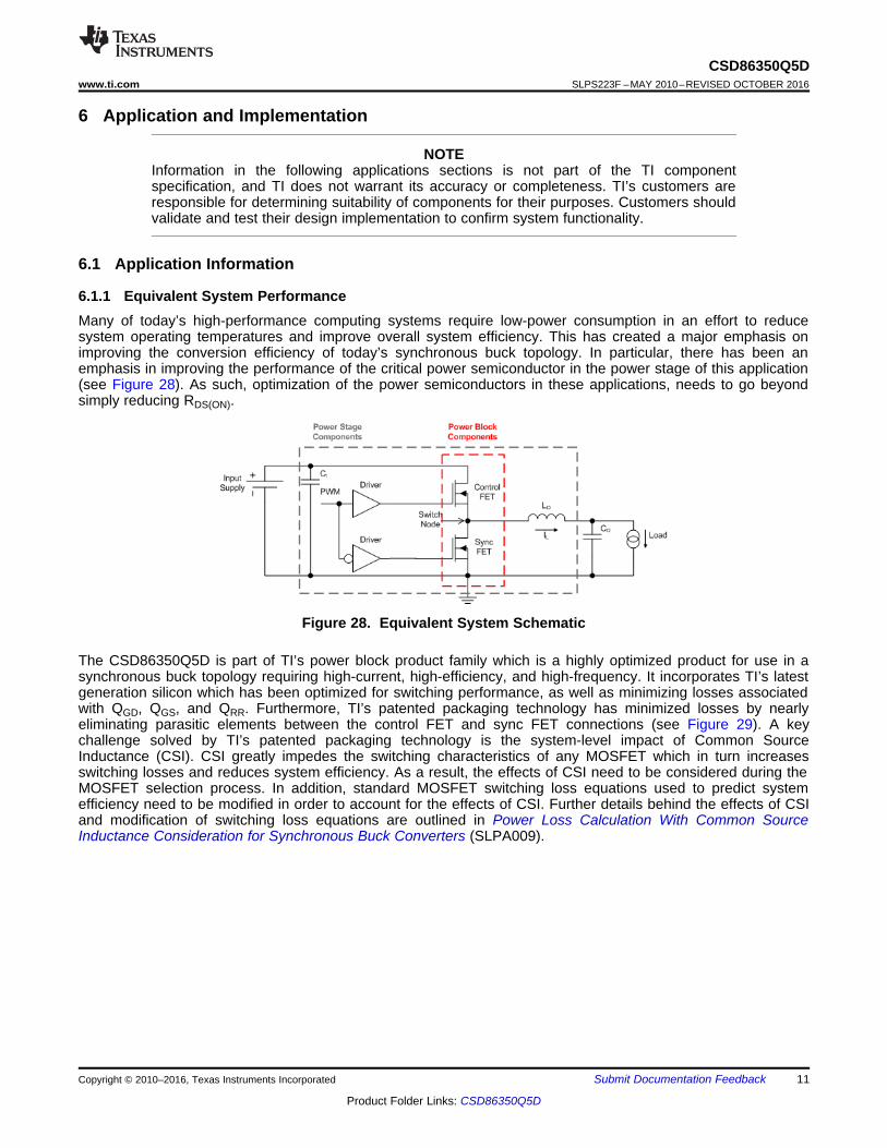
6.1.1 Equivalent System PerformanceMany of today’s high-performance computing systems require low-power consumption in an effort to reducesystem operating temperatures and improve overall system efficiency. This has created a major emphasis onimproving the conversion efficiency of today’s synchronous buck topology. In particular, there has been anemphasis in improving the performance of the critical power semiconductor in the power stage of this application(see Figure 28). As such, optimization of the power semiconductors in these applications, needs to go beyondsimply reducing RDS(ON).
Figure 28. Equivalent System Schematic
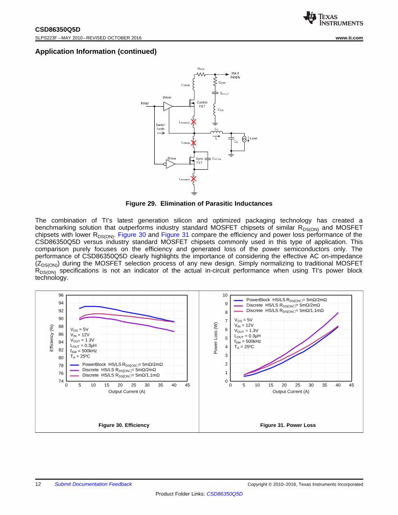
The CSD86350Q5D is part of TI’s power block product family which is a highly optimized product for use in asynchronous buck topology requiring high-current, high-efficiency, and high-frequency. It incorporates TI’s latestgeneration silicon which has been optimized for switching performance, as well as minimizing losses associatedwith QGD, QGS, and QRR. Furthermore, TI’s patented packaging technology has minimized losses by nearlyeliminating parasitic elements between the control FET and sync FET connections (see Figure 29). A keychallenge solved by TI’s patented packaging technology is the system-level impact of Common SourceInductance (CSI). CSI greatly impedes the switching characteristics of any MOSFET which in turn increasesswitching losses and reduces system efficiency. As a result, the effects of CSI need to be considered during theMOSFET selection process. In addition, standard MOSFET switching loss equations used to predict systemefficiency need to be modified in order to account for the effects of CSI. Further details behind the effects of CSIand modification of switching loss equations are outlined in Power Loss Calculation With Common SourceInductance Consideration for Synchronous Buck Converters (SLPA009).
74
76
78
80
82
84
86
88
90
92
94
96
0 5 10 15 20 25 30 35 40 45Output Current (A)
Effi
cien
cy (
%)
PowerBlock HS/LS RDS(ON) = 5mΩ/2mΩDiscrete HS/LS RDS(ON) = 5mΩ/2mΩDiscrete HS/LS RDS(ON) = 5mΩ/1.1mΩ
VGS = 5VVIN = 12VVOUT = 1.3VLOUT = 0.3µHfSW = 500kHzTA = 25ºC
0
1
2
3
4
5
6
7
8
9
10
0 5 10 15 20 25 30 35 40 45Output Current (A)
Pow
er L
oss
(W)
PowerBlock HS/LS RDS(ON) = 5mΩ/2mΩDiscrete HS/LS RDS(ON) = 5mΩ/2mΩDiscrete HS/LS RDS(ON) = 5mΩ/1.1mΩ
VGS = 5VVIN = 12VVOUT = 1.3VLOUT = 0.3µHfSW = 500kHzTA = 25ºC
12
CSD86350Q5DSLPS223F –MAY 2010–REVISED OCTOBER 2016 www.ti.com
Product Folder Links: CSD86350Q5D
Submit Documentation Feedback Copyright © 2010–2016, Texas Instruments Incorporated
Application Information (continued)
Figure 29. Elimination of Parasitic Inductances
The combination of TI’s latest generation silicon and optimized packaging technology has created abenchmarking solution that outperforms industry standard MOSFET chipsets of similar RDS(ON) and MOSFETchipsets with lower RDS(ON). Figure 30 and Figure 31 compare the efficiency and power loss performance of theCSD86350Q5D versus industry standard MOSFET chipsets commonly used in this type of application. Thiscomparison purely focuses on the efficiency and generated loss of the power semiconductors only. Theperformance of CSD86350Q5D clearly highlights the importance of considering the effective AC on-impedance(ZDS(ON)) during the MOSFET selection process of any new design. Simply normalizing to traditional MOSFETRDS(ON) specifications is not an indicator of the actual in-circuit performance when using TI’s power blocktechnology.
Figure 30. Efficiency Figure 31. Power Loss

13
CSD86350Q5Dwww.ti.com SLPS223F –MAY 2010–REVISED OCTOBER 2016
Product Folder Links: CSD86350Q5D
Submit Documentation FeedbackCopyright © 2010–2016, Texas Instruments Incorporated
Application Information (continued)Table 1 below compares the traditional DC measured RDS(ON) of CSD86350Q5D versus its ZDS(ON). Thiscomparison takes into account the improved efficiency associated with TI’s patented packaging technology. Assuch, when comparing TI’s power block products to individually packaged discrete MOSFETs or dual MOSFETsin a standard package, the in-circuit switching performance of the solution must be considered. In this example,individually packaged discrete MOSFETs or dual MOSFETs in a standard package would need to have DCmeasured RDS(ON) values that are equivalent to CSD86350Q5D’s ZDS(ON) value in order to have the sameefficiency performance at full load. Mid to light-load efficiency will still be lower with individually packaged discreteMOSFETs or dual MOSFETs in a standard package.
Table 1. Comparison of RDS(ON) vs. ZDS(ON)
PARAMETERHS LS
TYP MAX TYP MAXEffective AC on-impedance (ZDS(ON)), VGS = 5 V 5 — 1.1 —
DC measured RDS(ON), VGS = 4.5 V 5 6.6 2 2.7
The CSD86350Q5D NexFET™ power block is an optimized design for synchronous buck applications using 5-Vgate drive. The control FET and sync FET silicon are parametrically tuned to yield the lowest power loss andhighest system efficiency. As a result, a new rating method is needed which is tailored towards a more systems-centric environment. System-level performance curves such as power loss, Safe Operating Area (SOA), andnormalized graphs allow engineers to predict the product performance in the actual application.
6.1.2 Power Loss CurvesMOSFET centric parameters such as RDS(ON) and Qgd are needed to estimate the loss generated by the devices.In an effort to simplify the design process for engineers, Texas Instruments has provided measured power lossperformance curves. Figure 1 plots the power loss of the CSD86350Q5D as a function of load current. This curveis measured by configuring and running the CSD86350Q5D as it would be in the final application (seeFigure 32).The measured power loss is the CSD86350Q5D loss and consists of both input conversion loss andgate drive loss. Equation 1 is used to generate the power loss curve.
(VIN x IIN) + (VDD x IDD) – (VSW_AVG x IOUT) = Power Loss (1)
The power loss curve in Figure 1 is measured at the maximum recommended junction temperatures of 125°Cunder isothermal test conditions.
6.1.3 Safe Operating Area (SOA) CurvesThe SOA curves in the CSD86350Q5D data sheet provides guidance on the temperature boundaries within anoperating system by incorporating the thermal resistance and system power loss. Figure 3 to Figure 5 outline thetemperature and airflow conditions required for a given load current. The area under the curve dictates the safeoperating area. All the curves are based on measurements made on a PCB design with dimensions of 4 in (W) ×3.5 in (L) × 0.062 in (T) and 6 copper layers of 1-oz copper thickness.
6.1.4 Normalized CurvesThe normalized curves in the CSD86350Q5D data sheet provides guidance on the power loss and SOAadjustments based on their application specific needs. These curves show how the power loss and SOAboundaries will adjust for a given set of systems conditions. The primary Y-axis is the normalized change inpower loss and the secondary Y-axis is the change in system temperature required in order to comply with theSOA curve. The change in power loss is a multiplier for the power loss curve and the change in temperature issubtracted from the SOA curve.
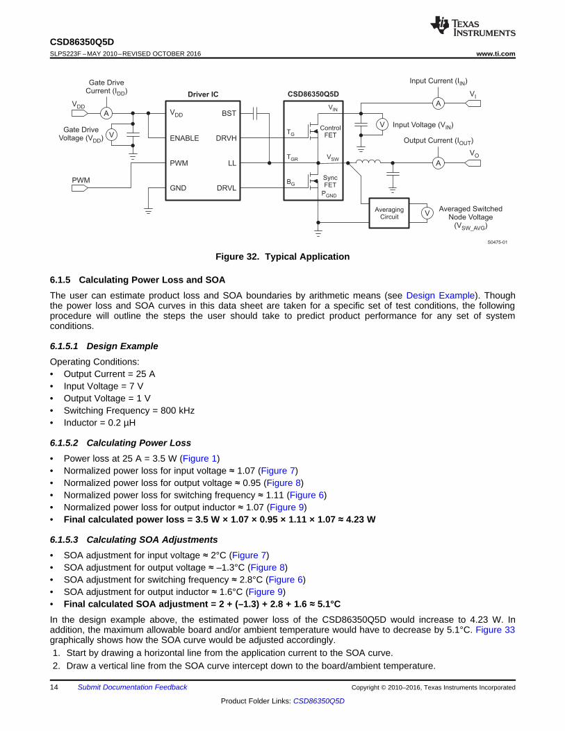
PWM
ENABLE
PWM
GND
BST
DRVH
LL
DRVL
CSD86350Q5DDriver IC
VDD
Gate DriveCurrent (I )DD
Input Current (I )IN
Input Voltage (V )IN
Output Current (I )OUT
TGR
VIN
PGND
VI
VOVSW
TG
BG
Gate DriveVoltage (V )DD
VDDA
V
V
V
ControlFET
SyncFET
AveragingCircuit
Averaged SwitchedNode Voltage
(VSW_AVG)
A
S0475-01
A
14
CSD86350Q5DSLPS223F –MAY 2010–REVISED OCTOBER 2016 www.ti.com
Product Folder Links: CSD86350Q5D
Submit Documentation Feedback Copyright © 2010–2016, Texas Instruments Incorporated
Figure 32. Typical Application
6.1.5 Calculating Power Loss and SOAThe user can estimate product loss and SOA boundaries by arithmetic means (see Design Example). Thoughthe power loss and SOA curves in this data sheet are taken for a specific set of test conditions, the followingprocedure will outline the steps the user should take to predict product performance for any set of systemconditions.
6.1.5.1 Design ExampleOperating Conditions:• Output Current = 25 A• Input Voltage = 7 V• Output Voltage = 1 V• Switching Frequency = 800 kHz• Inductor = 0.2 µH
6.1.5.2 Calculating Power Loss• Power loss at 25 A = 3.5 W (Figure 1)• Normalized power loss for input voltage ≈ 1.07 (Figure 7)• Normalized power loss for output voltage ≈ 0.95 (Figure 8)• Normalized power loss for switching frequency ≈ 1.11 (Figure 6)• Normalized power loss for output inductor ≈ 1.07 (Figure 9)• Final calculated power loss = 3.5 W × 1.07 × 0.95 × 1.11 × 1.07 ≈ 4.23 W
6.1.5.3 Calculating SOA Adjustments• SOA adjustment for input voltage ≈ 2°C (Figure 7)• SOA adjustment for output voltage ≈ –1.3°C (Figure 8)• SOA adjustment for switching frequency ≈ 2.8°C (Figure 6)• SOA adjustment for output inductor ≈ 1.6°C (Figure 9)• Final calculated SOA adjustment = 2 + (–1.3) + 2.8 + 1.6 ≈ 5.1°CIn the design example above, the estimated power loss of the CSD86350Q5D would increase to 4.23 W. Inaddition, the maximum allowable board and/or ambient temperature would have to decrease by 5.1°C. Figure 33graphically shows how the SOA curve would be adjusted accordingly.1. Start by drawing a horizontal line from the application current to the SOA curve.2. Draw a vertical line from the SOA curve intercept down to the board/ambient temperature.

Board Temperature (°C)0 20 40 60 80 100 120 140
0
5
10
15
20
25
30
35
40
45
50
G028
V = 12VIN
V = 5VGS
V = 1.3VOUT
f = 500kHzSW
L = 0.3 mHOUT
Outp
ut
Curr
ent
(A)
1
2
3
15
CSD86350Q5Dwww.ti.com SLPS223F –MAY 2010–REVISED OCTOBER 2016
Product Folder Links: CSD86350Q5D
Submit Documentation FeedbackCopyright © 2010–2016, Texas Instruments Incorporated
3. Adjust the SOA board/ambient temperature by subtracting the temperature adjustment value.
In the design example, the SOA temperature adjustment yields a reduction in allowable board/ambienttemperature of 5.1°C. In the event the adjustment value is a negative number, subtracting the negative numberwould yield an increase in allowable board/ambient temperature.
Figure 33. Power Block SOA
16
CSD86350Q5DSLPS223F –MAY 2010–REVISED OCTOBER 2016 www.ti.com
Product Folder Links: CSD86350Q5D
Submit Documentation Feedback Copyright © 2010–2016, Texas Instruments Incorporated
(1) Keong W. Kam, David Pommerenke, “EMI Analysis Methods for Synchronous Buck Converter EMI Root Cause Analysis”, University ofMissouri – Rolla
7 Layout
7.1 Layout GuidelinesThere are two key system-level parameters that can be addressed with a proper PCB design: electrical andthermal performance. Properly optimizing the PCB layout will yield maximum performance in both areas. A briefdescription on how to address each parameter is provided.
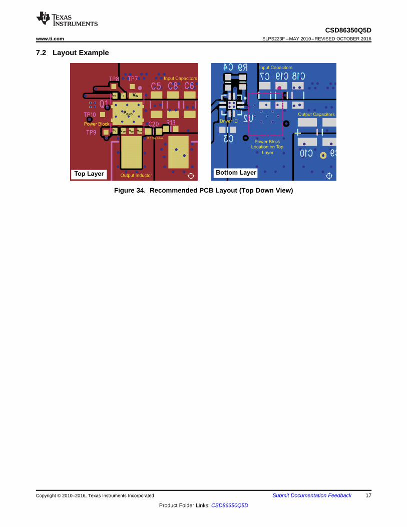
7.1.1 Electrical PerformanceThe power block has the ability to switch voltages at rates greater than 10 kV/µs. Special care must be thentaken with the PCB layout design and placement of the input capacitors, driver IC, and output inductor.• The placement of the input capacitors relative to the power block’s VIN and PGND pins should have the
highest priority during the component placement routine. It is critical to minimize these node lengths. As such,ceramic input capacitors need to be placed as close as possible to the VIN and PGND pins (see Figure 34).The example in Figure 34 uses 6 × 10-µF ceramic capacitors (TDK part C3216X5R1C106KT or equivalent).Notice there are ceramic capacitors on both sides of the board with an appropriate amount of viasinterconnecting both layers. In terms of priority of placement next to the power block, C5, C7, C19, and C8should follow in order.
• The driver IC should be placed relatively close to the power block gate pins. TG and BG should connect to theoutputs of the driver IC. The TGR pin serves as the return path of the high-side gate drive circuitry and shouldbe connected to the phase pin of the IC (sometimes called LX, LL, SW, PH, etc.). The bootstrap capacitor forthe driver IC will also connect to this pin.
• The switching node of the output inductor should be placed relatively close to the power block VSW pins.Minimizing the node length between these two components will reduce the PCB conduction losses andactually reduce the switching noise level. In the event the switch node waveform exhibits ringing that reachesundesirable levels, the use of a boost resistor or RC snubber can be an effective way to easily reduce thepeak ring level. The recommended boost resistor value will range between 1 Ω to 4.7 Ω depending on theoutput characteristics of driver IC used in conjunction with the power block. The RC snubber values canrange from 0.5 Ω to 2.2 Ω for the R and 330 pF to 2200 pF for the C. Please refer to Snubber Circuits:Theory, Design and Application (SLUP100) for more details on how to properly tune the RC snubber values.The RC snubber should be placed as close as possible to the VSW node and PGND see Figure 34. (1)
7.1.2 Thermal PerformanceThe power block has the ability to utilize the GND planes as the primary thermal path. As such, the use ofthermal vias is an effective way to pull away heat from the device and into the system board. Concerns of soldervoids and manufacturability problems can be addressed by the use of three basic tactics to minimize the amountof solder attach that will wick down the via barrel:• Intentionally space out the vias from each other to avoid a cluster of holes in a given area.• Use the smallest drill size allowed in your design. The example in Figure 34 uses vias with a 10-mil drill hole
and a 16-mil capture pad.• Tent the opposite side of the via with solder-mask.
In the end, the number and drill size of the thermal vias should align with the end user’s PCB design rules andmanufacturing capabilities.
VIN
V SW
PGND
BG
TGTGR
VSW V SW
Output Inductor
Input Capacitors
Power Block
Input Capacitors
Output Capacitors
Driver IC
Bottom LayerTop Layer
RC Snubber
Power BlockLocation on Top
Layer
17
CSD86350Q5Dwww.ti.com SLPS223F –MAY 2010–REVISED OCTOBER 2016
Product Folder Links: CSD86350Q5D
Submit Documentation FeedbackCopyright © 2010–2016, Texas Instruments Incorporated
7.2 Layout Example
Figure 34. Recommended PCB Layout (Top Down View)

18
CSD86350Q5DSLPS223F –MAY 2010–REVISED OCTOBER 2016 www.ti.com
Product Folder Links: CSD86350Q5D
Submit Documentation Feedback Copyright © 2010–2016, Texas Instruments Incorporated
8 Device and Documentation Support
8.1 Documentation Support
8.1.1 Related DocumentationFor related documentation see the following:• Power Loss Calculation With Common Source Inductance Consideration for Synchronous Buck Converters
(SLPA009)• Snubber Circuits: Theory, Design and Application (SLUP100)
8.2 Receiving Notification of Documentation UpdatesTo receive notification of documentation updates, navigate to the device product folder on ti.com. In the upperright corner, click on Alert me to register and receive a weekly digest of any product information that haschanged. For change details, review the revision history included in any revised document.
8.3 Community ResourcesThe following links connect to TI community resources. Linked contents are provided "AS IS" by the respectivecontributors. They do not constitute TI specifications and do not necessarily reflect TI's views; see TI's Terms ofUse.
TI E2E™ Online Community TI's Engineer-to-Engineer (E2E) Community. Created to foster collaborationamong engineers. At e2e.ti.com, you can ask questions, share knowledge, explore ideas and helpsolve problems with fellow engineers.
Design Support TI's Design Support Quickly find helpful E2E forums along with design support tools andcontact information for technical support.
8.4 TrademarksNexFET, E2E are trademarks of Texas Instruments.All other trademarks are the property of their respective owners.
8.5 GlossarySLYZ022 — TI Glossary.
This glossary lists and explains terms, acronyms, and definitions.
M0187-01
E1
E
q
c
56
78 1
23
4
L
d1
f
K
b
d3
L
E1
e
a
E2
D2
Top View Bottom View
Front View
Side View
5
9
67
8
12
34
qc1
D1
d2
d
Pinout
Position Designation
Pin 1 VIN
Pin 2 VIN
Pin 3 TG
Pin 4 TGR
Pin 5 BG
Pin 6 VSW
Pin 7 VSW
Pin 8 VSW
Pin 9 PGND
Exposed Tie Bar May Vary
19
CSD86350Q5Dwww.ti.com SLPS223F –MAY 2010–REVISED OCTOBER 2016
Product Folder Links: CSD86350Q5D
Submit Documentation FeedbackCopyright © 2010–2016, Texas Instruments Incorporated
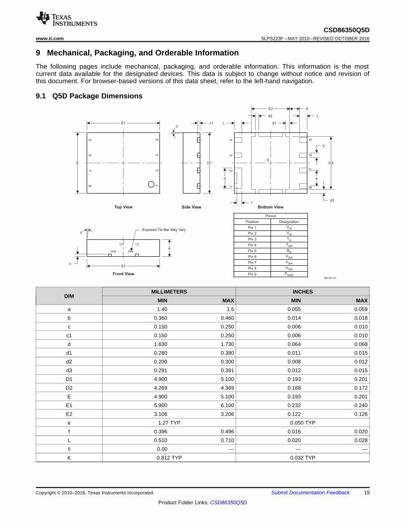
9 Mechanical, Packaging, and Orderable InformationThe following pages include mechanical, packaging, and orderable information. This information is the mostcurrent data available for the designated devices. This data is subject to change without notice and revision ofthis document. For browser-based versions of this data sheet, refer to the left-hand navigation.
9.1 Q5D Package Dimensions
DIMMILLIMETERS INCHES
MIN MAX MIN MAXa 1.40 1.5 0.055 0.059b 0.360 0.460 0.014 0.018c 0.150 0.250 0.006 0.010
c1 0.150 0.250 0.006 0.010d 1.630 1.730 0.064 0.068d1 0.280 0.380 0.011 0.015d2 0.200 0.300 0.008 0.012d3 0.291 0.391 0.012 0.015D1 4.900 5.100 0.193 0.201D2 4.269 4.369 0.168 0.172E 4.900 5.100 0.193 0.201E1 5.900 6.100 0.232 0.240E2 3.106 3.206 0.122 0.126e 1.27 TYP 0.050 TYPf 0.396 0.496 0.016 0.020L 0.510 0.710 0.020 0.028θ 0.00 — — —K 0.812 TYP 0.032 TYP
M0208-01
0.341 (0.013)
0.410 (0.016)
14
58
0.250 (0.010)
0.300 (0.012)
0.300 (0.012)
Stencil Opening0.300 (0.012)
0.950 (0.037)
PCB Pattern
1.290 (0.051)
0.610 (0.024)
1.680(0.066)
1.710(0.067)
M0188-01
0.650 (0.026)0.650 (0.026)
0.620 (0.024)0.620
(0.024)
0.415 (0.016)
14
58
0.345 (0.014)
3.480 (0.137)
0.850 (0.033) 0.850 (0.033)
0.530 (0.021)
0.400 (0.016)
6.240 (0.246)
1.920(0.076)
4.460(0.176)
4.460(0.176)
1.270(0.050)
20
CSD86350Q5DSLPS223F –MAY 2010–REVISED OCTOBER 2016 www.ti.com
Product Folder Links: CSD86350Q5D
Submit Documentation Feedback Copyright © 2010–2016, Texas Instruments Incorporated
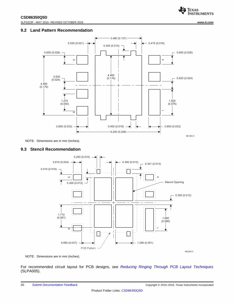
9.2 Land Pattern Recommendation
NOTE: Dimensions are in mm (inches).
9.3 Stencil Recommendation
NOTE: Dimensions are in mm (inches).
.For recommended circuit layout for PCB designs, see Reducing Ringing Through PCB Layout Techniques(SLPA005).
Ø 1.50+0.10–0.00
4.00 ±0.10 (See Note 1)
1.75 ±0.10
R 0.30 TYPØ 1.50 MINA0
K0
0.30 ±0.05
R 0.20 MAX
A0 = 5.30 ±0.10B0 = 6.50 ±0.10K0 = 1.90 ±0.10
M0191-01
2.00 ±0.05
8.00 ±0.10
B0
5.50 ±0.05
12.00 ±0.30
21
CSD86350Q5Dwww.ti.com SLPS223F –MAY 2010–REVISED OCTOBER 2016
Product Folder Links: CSD86350Q5D
Submit Documentation FeedbackCopyright © 2010–2016, Texas Instruments Incorporated
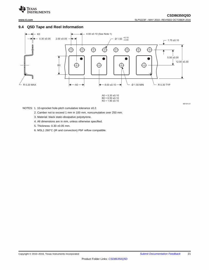
9.4 Q5D Tape and Reel Information
NOTES: 1. 10-sprocket hole-pitch cumulative tolerance ±0.2.2. Camber not to exceed 1 mm in 100 mm, noncumulative over 250 mm.3. Material: black static-dissipative polystyrene.4. All dimensions are in mm, unless otherwise specified.5. Thickness: 0.30 ±0.05 mm.6. MSL1 260°C (IR and convection) PbF reflow compatible.
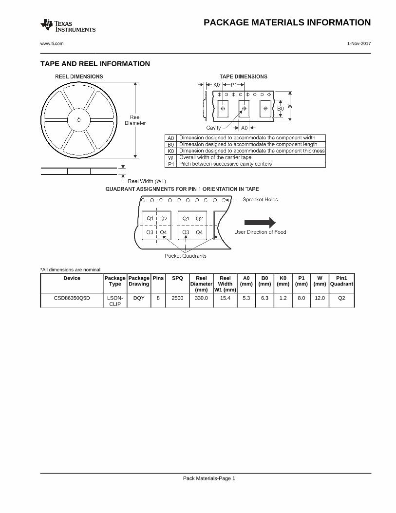
TAPE AND REEL INFORMATION
*All dimensions are nominal
Device PackageType
PackageDrawing
Pins SPQ ReelDiameter
(mm)
ReelWidth
W1 (mm)
A0(mm)
B0(mm)
K0(mm)
P1(mm)
W(mm)
Pin1Quadrant
CSD86350Q5D LSON-CLIP
DQY 8 2500 330.0 15.4 5.3 6.3 1.2 8.0 12.0 Q2
PACKAGE MATERIALS INFORMATION
www.ti.com 1-Nov-2017
Pack Materials-Page 1
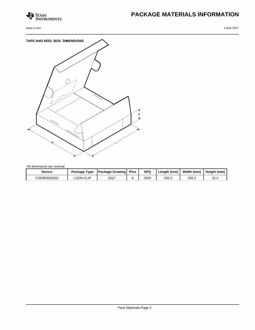
*All dimensions are nominal
Device Package Type Package Drawing Pins SPQ Length (mm) Width (mm) Height (mm)
CSD86350Q5D LSON-CLIP DQY 8 2500 335.0 335.0 32.0
PACKAGE MATERIALS INFORMATION
www.ti.com 1-Nov-2017
Pack Materials-Page 2

IMPORTANT NOTICE
Texas Instruments Incorporated (TI) reserves the right to make corrections, enhancements, improvements and other changes to itssemiconductor products and services per JESD46, latest issue, and to discontinue any product or service per JESD48, latest issue. Buyersshould obtain the latest relevant information before placing orders and should verify that such information is current and complete.TI’s published terms of sale for semiconductor products (http://www.ti.com/sc/docs/stdterms.htm) apply to the sale of packaged integratedcircuit products that TI has qualified and released to market. Additional terms may apply to the use or sale of other types of TI products andservices.Reproduction of significant portions of TI information in TI data sheets is permissible only if reproduction is without alteration and isaccompanied by all associated warranties, conditions, limitations, and notices. TI is not responsible or liable for such reproduceddocumentation. Information of third parties may be subject to additional restrictions. Resale of TI products or services with statementsdifferent from or beyond the parameters stated by TI for that product or service voids all express and any implied warranties for theassociated TI product or service and is an unfair and deceptive business practice. TI is not responsible or liable for any such statements.Buyers and others who are developing systems that incorporate TI products (collectively, “Designers”) understand and agree that Designersremain responsible for using their independent analysis, evaluation and judgment in designing their applications and that Designers havefull and exclusive responsibility to assure the safety of Designers' applications and compliance of their applications (and of all TI productsused in or for Designers’ applications) with all applicable regulations, laws and other applicable requirements. Designer represents that, withrespect to their applications, Designer has all the necessary expertise to create and implement safeguards that (1) anticipate dangerousconsequences of failures, (2) monitor failures and their consequences, and (3) lessen the likelihood of failures that might cause harm andtake appropriate actions. Designer agrees that prior to using or distributing any applications that include TI products, Designer willthoroughly test such applications and the functionality of such TI products as used in such applications.TI’s provision of technical, application or other design advice, quality characterization, reliability data or other services or information,including, but not limited to, reference designs and materials relating to evaluation modules, (collectively, “TI Resources”) are intended toassist designers who are developing applications that incorporate TI products; by downloading, accessing or using TI Resources in anyway, Designer (individually or, if Designer is acting on behalf of a company, Designer’s company) agrees to use any particular TI Resourcesolely for this purpose and subject to the terms of this Notice.TI’s provision of TI Resources does not expand or otherwise alter TI’s applicable published warranties or warranty disclaimers for TIproducts, and no additional obligations or liabilities arise from TI providing such TI Resources. TI reserves the right to make corrections,enhancements, improvements and other changes to its TI Resources. TI has not conducted any testing other than that specificallydescribed in the published documentation for a particular TI Resource.Designer is authorized to use, copy and modify any individual TI Resource only in connection with the development of applications thatinclude the TI product(s) identified in such TI Resource. NO OTHER LICENSE, EXPRESS OR IMPLIED, BY ESTOPPEL OR OTHERWISETO ANY OTHER TI INTELLECTUAL PROPERTY RIGHT, AND NO LICENSE TO ANY TECHNOLOGY OR INTELLECTUAL PROPERTYRIGHT OF TI OR ANY THIRD PARTY IS GRANTED HEREIN, including but not limited to any patent right, copyright, mask work right, orother intellectual property right relating to any combination, machine, or process in which TI products or services are used. Informationregarding or referencing third-party products or services does not constitute a license to use such products or services, or a warranty orendorsement thereof. Use of TI Resources may require a license from a third party under the patents or other intellectual property of thethird party, or a license from TI under the patents or other intellectual property of TI.TI RESOURCES ARE PROVIDED “AS IS” AND WITH ALL FAULTS. TI DISCLAIMS ALL OTHER WARRANTIES ORREPRESENTATIONS, EXPRESS OR IMPLIED, REGARDING RESOURCES OR USE THEREOF, INCLUDING BUT NOT LIMITED TOACCURACY OR COMPLETENESS, TITLE, ANY EPIDEMIC FAILURE WARRANTY AND ANY IMPLIED WARRANTIES OFMERCHANTABILITY, FITNESS FOR A PARTICULAR PURPOSE, AND NON-INFRINGEMENT OF ANY THIRD PARTY INTELLECTUALPROPERTY RIGHTS. TI SHALL NOT BE LIABLE FOR AND SHALL NOT DEFEND OR INDEMNIFY DESIGNER AGAINST ANY CLAIM,INCLUDING BUT NOT LIMITED TO ANY INFRINGEMENT CLAIM THAT RELATES TO OR IS BASED ON ANY COMBINATION OFPRODUCTS EVEN IF DESCRIBED IN TI RESOURCES OR OTHERWISE. IN NO EVENT SHALL TI BE LIABLE FOR ANY ACTUAL,DIRECT, SPECIAL, COLLATERAL, INDIRECT, PUNITIVE, INCIDENTAL, CONSEQUENTIAL OR EXEMPLARY DAMAGES INCONNECTION WITH OR ARISING OUT OF TI RESOURCES OR USE THEREOF, AND REGARDLESS OF WHETHER TI HAS BEENADVISED OF THE POSSIBILITY OF SUCH DAMAGES.Unless TI has explicitly designated an individual product as meeting the requirements of a particular industry standard (e.g., ISO/TS 16949and ISO 26262), TI is not responsible for any failure to meet such industry standard requirements.Where TI specifically promotes products as facilitating functional safety or as compliant with industry functional safety standards, suchproducts are intended to help enable customers to design and create their own applications that meet applicable functional safety standardsand requirements. Using products in an application does not by itself establish any safety features in the application. Designers mustensure compliance with safety-related requirements and standards applicable to their applications. Designer may not use any TI products inlife-critical medical equipment unless authorized officers of the parties have executed a special contract specifically governing such use.Life-critical medical equipment is medical equipment where failure of such equipment would cause serious bodily injury or death (e.g., lifesupport, pacemakers, defibrillators, heart pumps, neurostimulators, and implantables). Such equipment includes, without limitation, allmedical devices identified by the U.S. Food and Drug Administration as Class III devices and equivalent classifications outside the U.S.TI may expressly designate certain products as completing a particular qualification (e.g., Q100, Military Grade, or Enhanced Product).Designers agree that it has the necessary expertise to select the product with the appropriate qualification designation for their applicationsand that proper product selection is at Designers’ own risk. Designers are solely responsible for compliance with all legal and regulatoryrequirements in connection with such selection.Designer will fully indemnify TI and its representatives against any damages, costs, losses, and/or liabilities arising out of Designer’s non-compliance with the terms and provisions of this Notice.
Mailing Address: Texas Instruments, Post Office Box 655303, Dallas, Texas 75265Copyright © 2017, Texas Instruments Incorporated
![Wireless Starter Kit Mainboard - Silicon Labs · vcom_enable pti0[0..2] vmcu gnd gnd gnd gnd vmcu vrf 5v 3v3 gnd vrf gnd gnd gnd gnd gnd usb_vbus usb_vreg usb_vbus 5v 5v_dbg …](https://img.pdfslide.net/doc/110x75/5ac0fbea7f8b9a4e7c8c7c14/wireless-starter-kit-mainboard-silicon-labs-pti002-vmcu-gnd-gnd-gnd-gnd-vmcu.jpg)