Embed Size (px)
Citation preview
CSE477 L05 IC Manufacturing.1 Irwin&Vijay, PSU, 2002
CSE477VLSI Digital Circuits
Fall 2002
Lecture 05: IC Manufacturing
Mary Jane Irwin ( www.cse.psu.edu/~mji ) www.cse.psu.edu/~cg477
[Adapted from Rabaey’s Digital Integrated Circuits, ©2002, J. Rabaey et al.]
CSE477 L05 IC Manufacturing.2 Irwin&Vijay, PSU, 2002
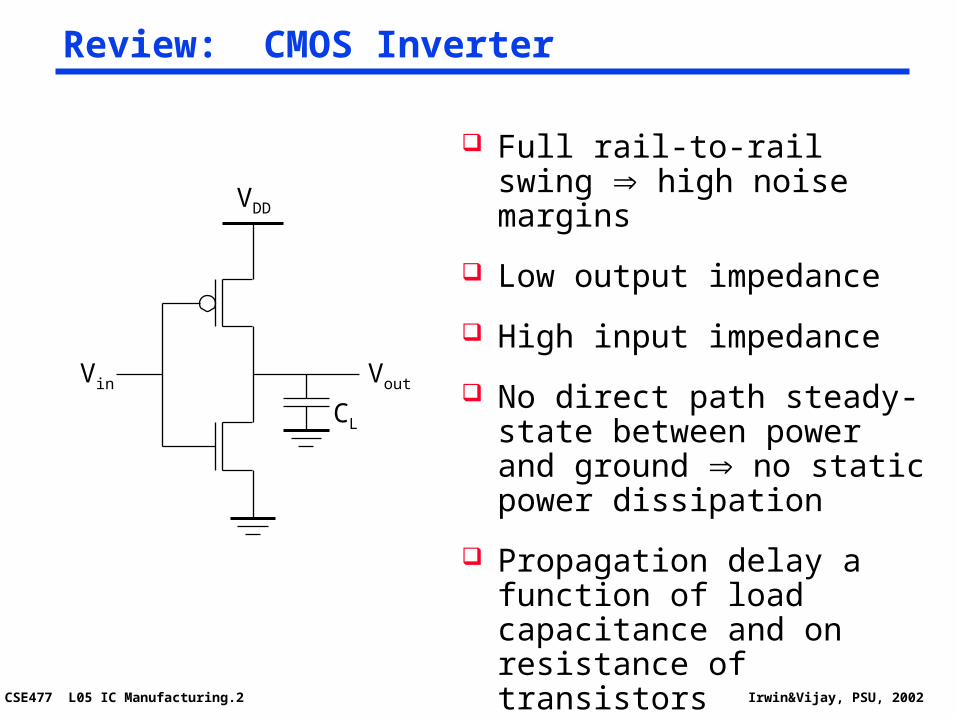
Review: CMOS Inverter
VDD
Vout
CL
Vin
Full rail-to-rail swing high noise margins
Low output impedance
High input impedance
No direct path steady-state between power and ground no static power dissipation
Propagation delay a function of load capacitance and on resistance of transistors
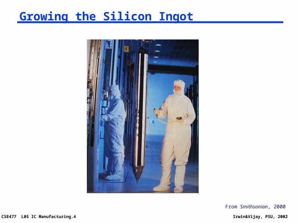
CSE477 L05 IC Manufacturing.4 Irwin&Vijay, PSU, 2002
Growing the Silicon Ingot
From Smithsonian, 2000
CSE477 L05 IC Manufacturing.5 Irwin&Vijay, PSU, 2002
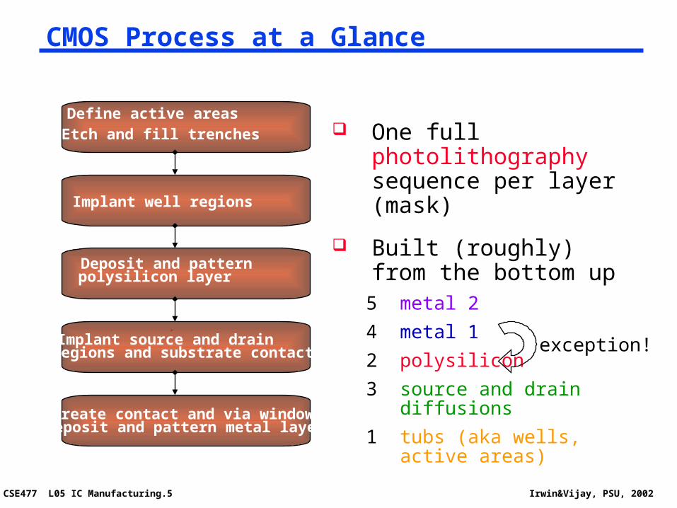
CMOS Process at a Glance
Define active areasEtch and fill trenches
Implant well regions
Deposit and patternpolysilicon layer
Implant source and drainregions and substrate contacts
Create contact and via windowsDeposit and pattern metal layers
One full photolithography sequence per layer (mask)
Built (roughly) from the bottom up
5 metal 2
4 metal 1
2 polysilicon
3 source and drain diffusions
1 tubs (aka wells, active areas)
exception!
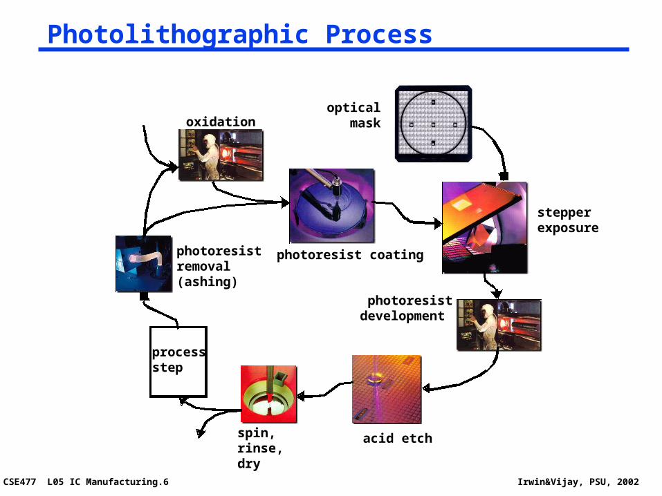
CSE477 L05 IC Manufacturing.6 Irwin&Vijay, PSU, 2002
oxidationoptical
mask
processstep
photoresist coatingphotoresist removal (ashing)
spin, rinse, dry
acid etch
photoresist development
stepper exposure
Photolithographic Process
CSE477 L05 IC Manufacturing.7 Irwin&Vijay, PSU, 2002
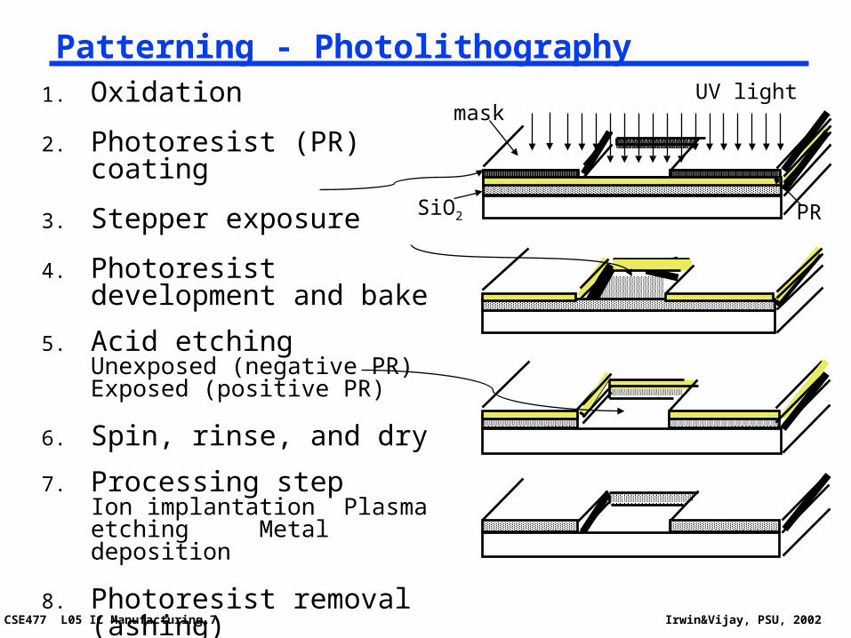
Patterning - Photolithography1. Oxidation
2. Photoresist (PR) coating
3. Stepper exposure
4. Photoresist development and bake
5. Acid etchingUnexposed (negative PR)Exposed (positive PR)
6. Spin, rinse, and dry
7. Processing stepIon implantationPlasma etchingMetal deposition
8. Photoresist removal (ashing)
mask
SiO2 PR
UV light
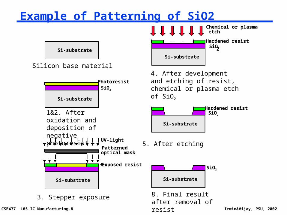
CSE477 L05 IC Manufacturing.8 Irwin&Vijay, PSU, 2002
Example of Patterning of SiO2
Si-substrate
Silicon base material
Si-substrate
3. Stepper exposure
UV-light
Patternedoptical mask
Exposed resist
1&2. After oxidation and deposition of negative photoresist
PhotoresistSiO2
Si-substrate
Si-substrate
SiO2
8. Final result after removal of resist
Si-substrate
SiO2
5. After etching
Hardened resist
SiO2
Si-substrate
4. After development and etching of resist, chemical or plasma etch of SiO2
Hardened resist
Chemical or plasmaetch
CSE477 L05 IC Manufacturing.9 Irwin&Vijay, PSU, 2002
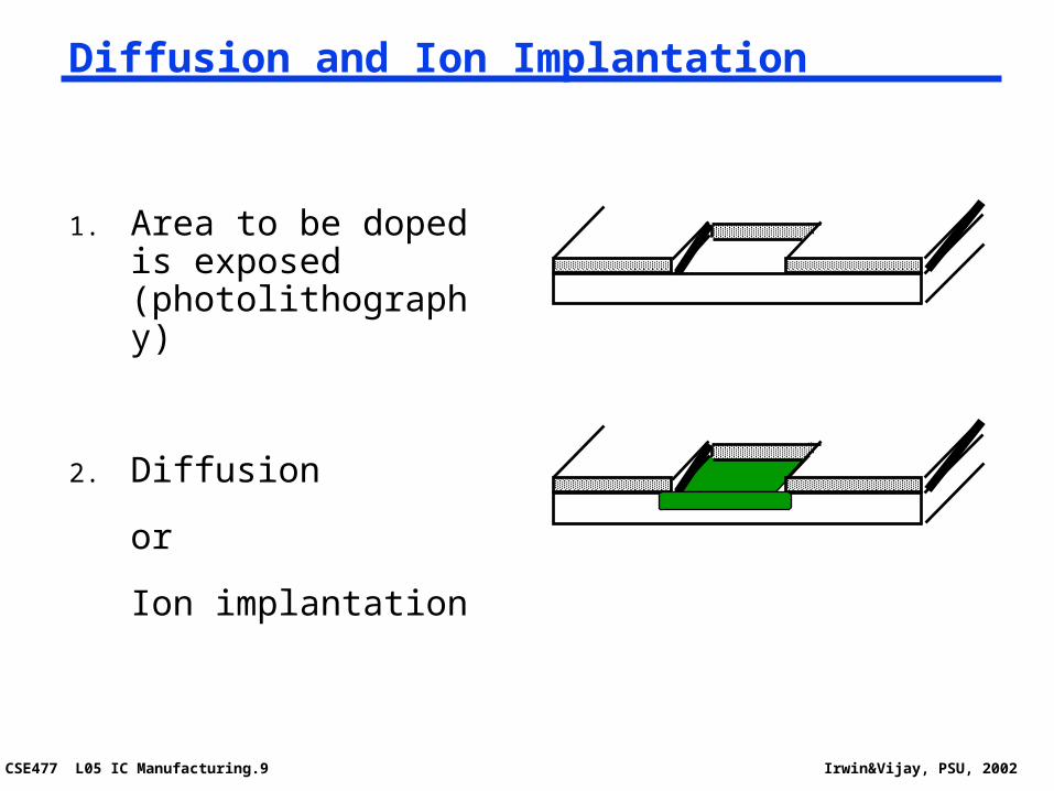
Diffusion and Ion Implantation
1. Area to be doped is exposed (photolithography)
2. Diffusion
or
Ion implantation
CSE477 L05 IC Manufacturing.10 Irwin&Vijay, PSU, 2002
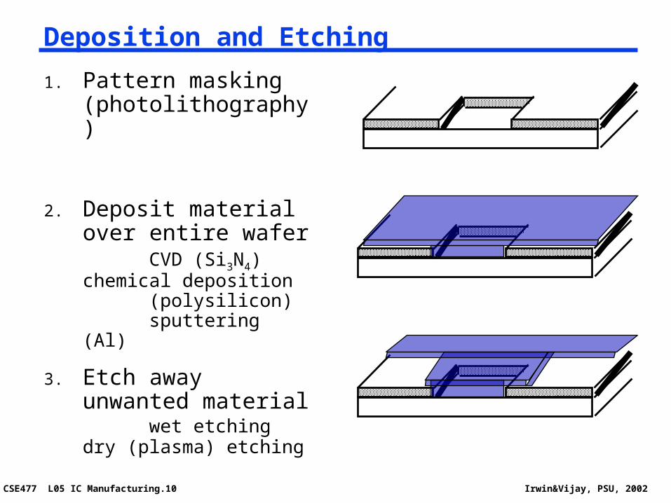
Deposition and Etching
1. Pattern masking (photolithography)
2. Deposit material over entire waferCVD (Si3N4)chemical deposition
(polysilicon)sputtering (Al)
3. Etch away unwanted material
wet etchingdry (plasma)
etching
CSE477 L05 IC Manufacturing.11 Irwin&Vijay, PSU, 2002
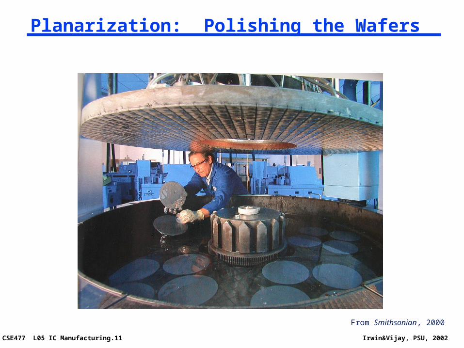
Planarization: Polishing the Wafers
From Smithsonian, 2000
CSE477 L05 IC Manufacturing.12 Irwin&Vijay, PSU, 2002
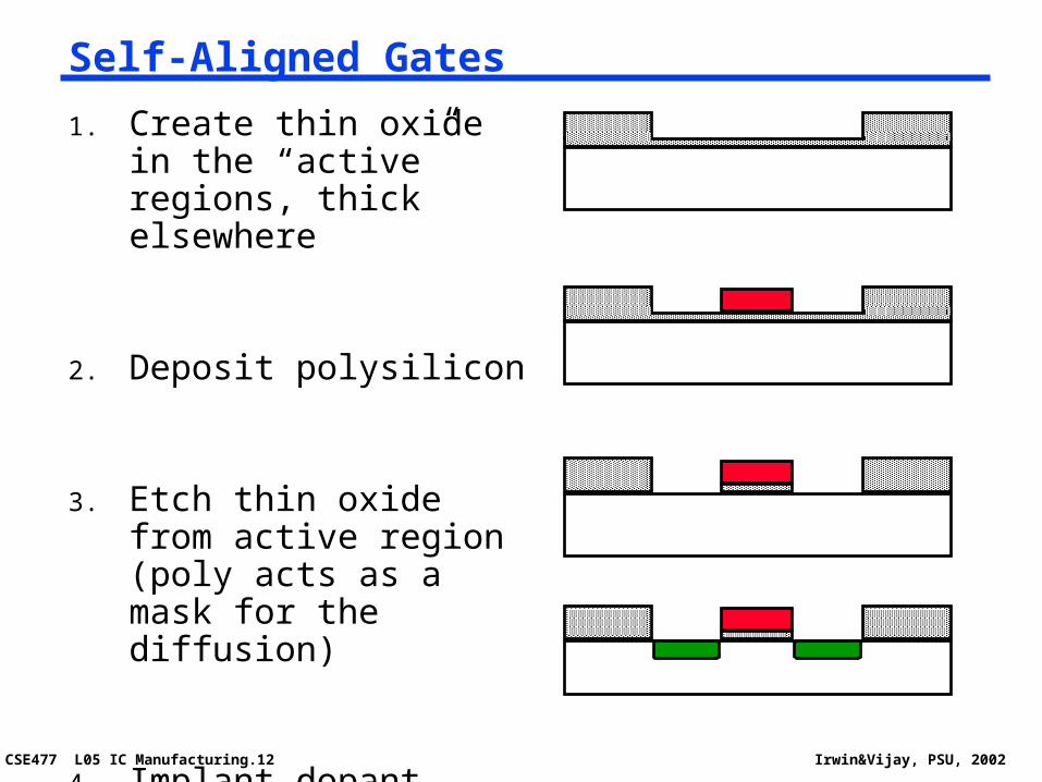
Self-Aligned Gates
1. Create thin oxide in the “active” regions, thick elsewhere
2. Deposit polysilicon
3. Etch thin oxide from active region (poly acts as a mask for the diffusion)
4. Implant dopant
CSE477 L05 IC Manufacturing.13 Irwin&Vijay, PSU, 2002
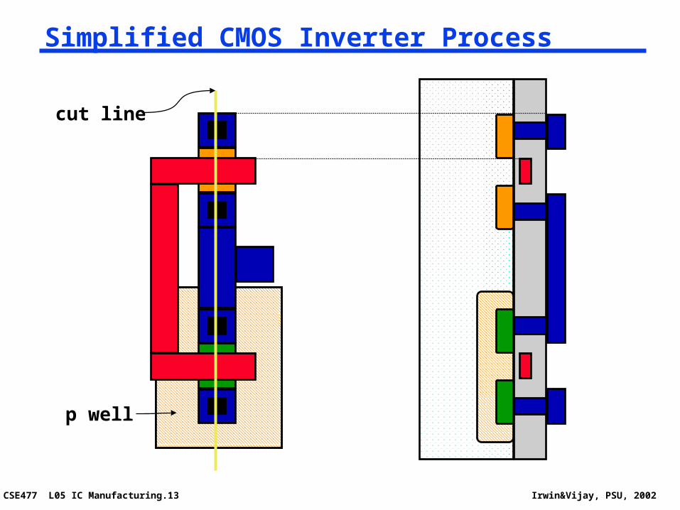
Simplified CMOS Inverter Process
cut line
p well
CSE477 L05 IC Manufacturing.14 Irwin&Vijay, PSU, 2002
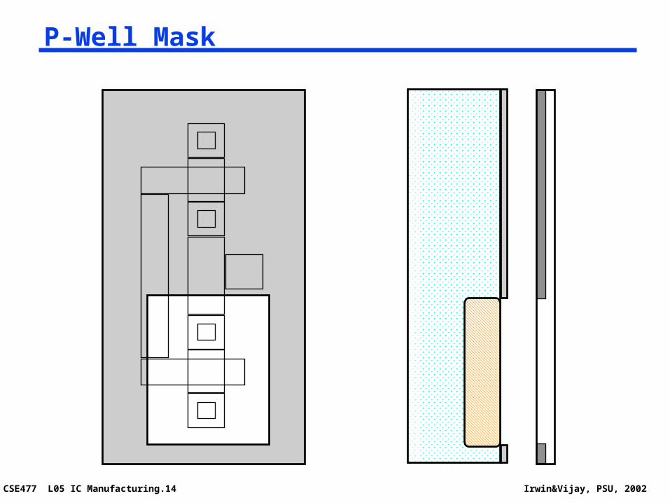
P-Well Mask
CSE477 L05 IC Manufacturing.15 Irwin&Vijay, PSU, 2002
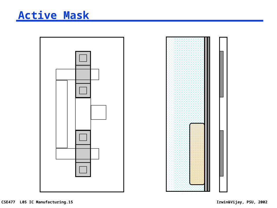
Active Mask
CSE477 L05 IC Manufacturing.16 Irwin&Vijay, PSU, 2002
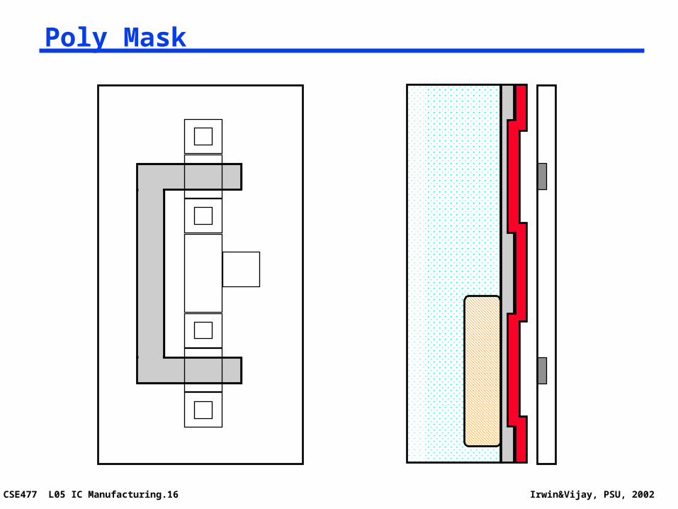
Poly Mask
CSE477 L05 IC Manufacturing.17 Irwin&Vijay, PSU, 2002
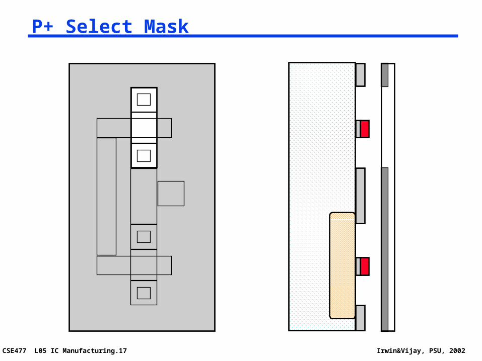
P+ Select Mask
CSE477 L05 IC Manufacturing.18 Irwin&Vijay, PSU, 2002
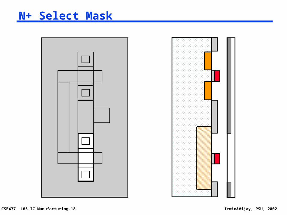
N+ Select Mask
CSE477 L05 IC Manufacturing.19 Irwin&Vijay, PSU, 2002
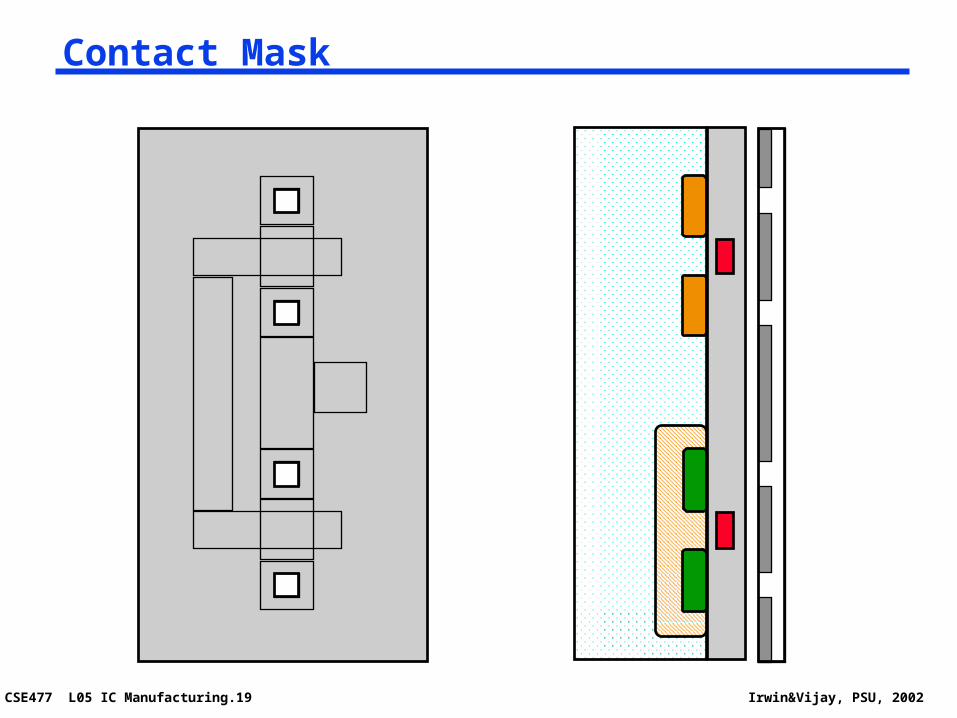
Contact Mask
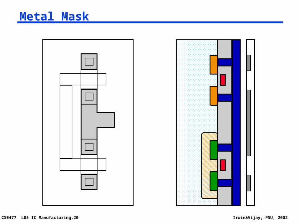
CSE477 L05 IC Manufacturing.20 Irwin&Vijay, PSU, 2002
Metal Mask
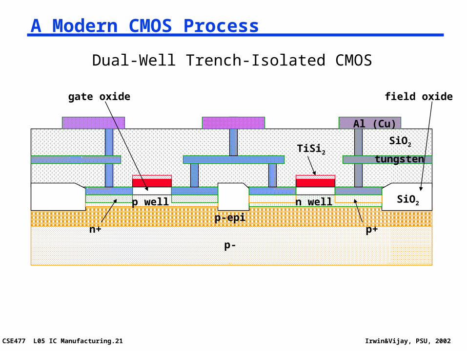
CSE477 L05 IC Manufacturing.21 Irwin&Vijay, PSU, 2002
A Modern CMOS Process
p-
p-epi
p well n well
p+n+
gate oxide
Al (Cu)
tungsten
SiO2
SiO2
TiSi2
Dual-Well Trench-Isolated CMOS
field oxide
CSE477 L05 IC Manufacturing.22 Irwin&Vijay, PSU, 2002
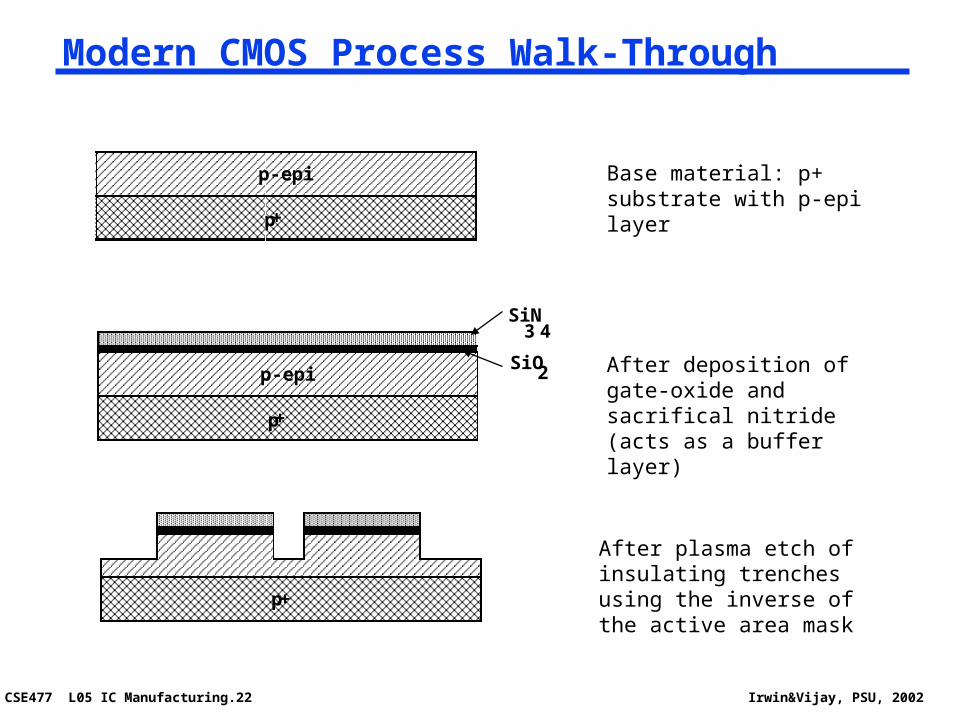
Modern CMOS Process Walk-Through
p+
p-epi Base material: p+ substrate with p-epi layer
p+
After plasma etch of insulating trenches using the inverse of the active area mask
p+
p-epiSiO2
3SiN
4
After deposition of gate-oxide and sacrifical nitride (acts as a buffer layer)
CSE477 L05 IC Manufacturing.23 Irwin&Vijay, PSU, 2002
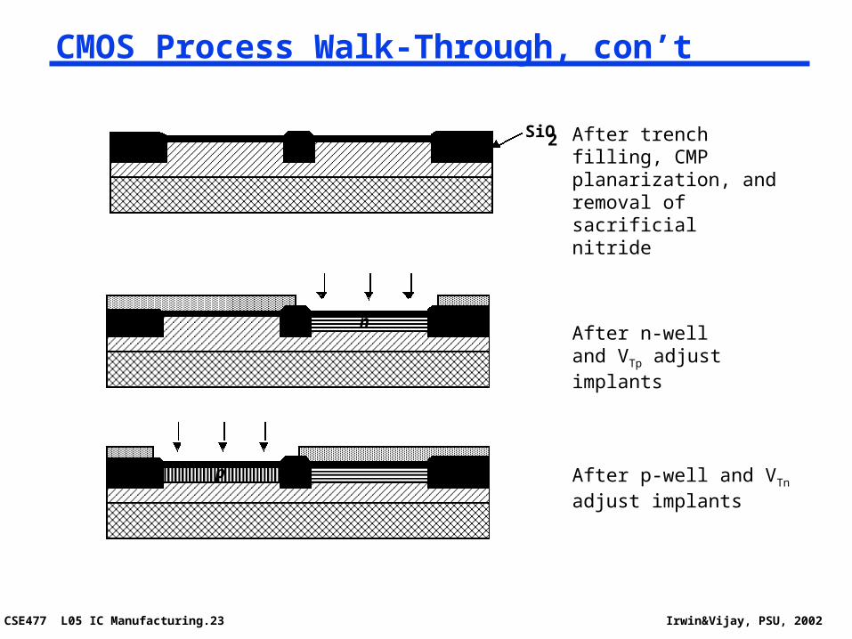
CMOS Process Walk-Through, con’t
SiO2 After trench filling, CMP planarization, and removal of sacrificial nitride
After n-well and VTp adjust implants
n
After p-well and VTn adjust implants
p
CSE477 L05 IC Manufacturing.24 Irwin&Vijay, PSU, 2002
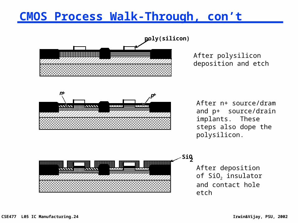
CMOS Process Walk-Through, con’t
After polysilicon deposition and etch
poly(silicon)
After n+ source/dram and p+ source/drain implants. These steps also dope the polysilicon.
p+n+
After deposition of SiO2 insulator and contact hole etch
SiO2
CSE477 L05 IC Manufacturing.25 Irwin&Vijay, PSU, 2002
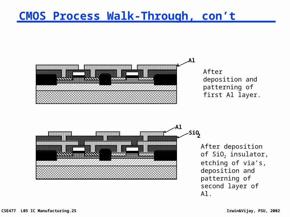
CMOS Process Walk-Through, con’t
After deposition and patterning of first Al layer.
Al
After deposition of SiO2 insulator, etching of via’s, deposition and patterning of second layer of Al.
AlSiO2
CSE477 L05 IC Manufacturing.26 Irwin&Vijay, PSU, 2002
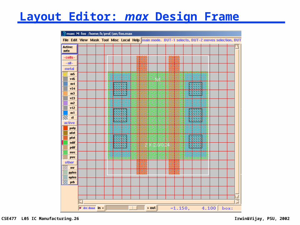
Layout Editor: max Design Frame
CSE477 L05 IC Manufacturing.27 Irwin&Vijay, PSU, 2002
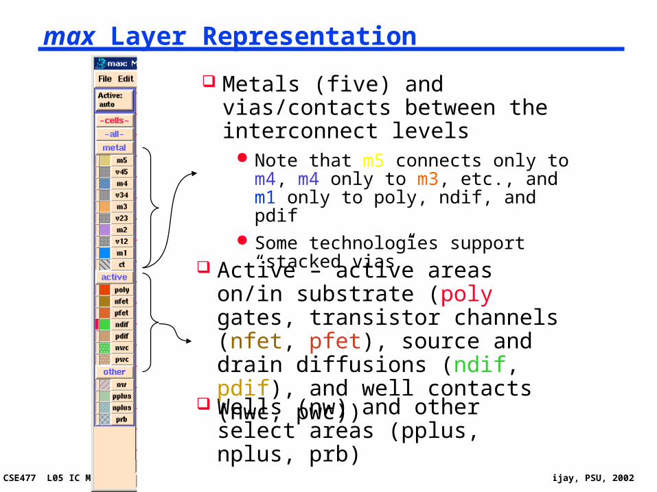
max Layer Representation
Metals (five) and vias/contacts between the interconnect levels
Note that m5 connects only to m4, m4 only to m3, etc., and m1 only to poly, ndif, and pdif
Some technologies support “stacked vias”
Wells (nw) and other select areas (pplus, nplus, prb)
Active – active areas on/in substrate (poly gates, transistor channels (nfet, pfet), source and drain diffusions (ndif, pdif), and well contacts (nwc, pwc))
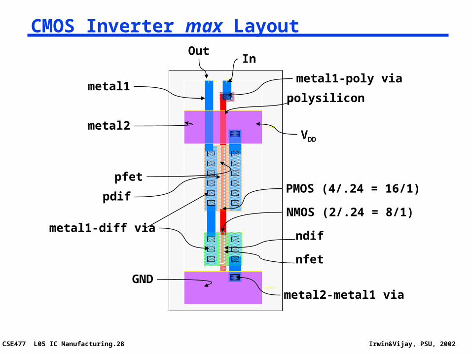
CSE477 L05 IC Manufacturing.28 Irwin&Vijay, PSU, 2002
CMOS Inverter max Layout
VDD
GND
NMOS (2/.24 = 8/1)
PMOS (4/.24 = 16/1)
metal2
metal1polysilicon
InOut
metal1-poly via
metal2-metal1 via
metal1-diff via
pfet
nfet
pdif
ndif
CSE477 L05 IC Manufacturing.29 Irwin&Vijay, PSU, 2002
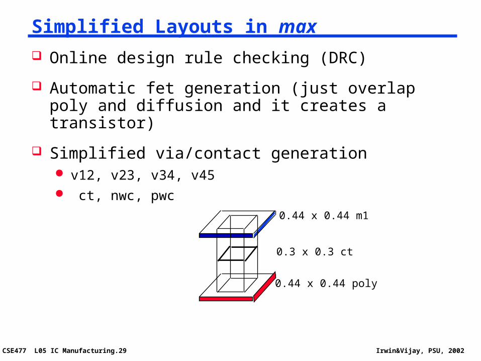
Simplified Layouts in max
Online design rule checking (DRC)
Automatic fet generation (just overlap poly and diffusion and it creates a transistor)
Simplified via/contact generation v12, v23, v34, v45 ct, nwc, pwc
0.44 x 0.44 m1
0.3 x 0.3 ct
0.44 x 0.44 poly
CSE477 L05 IC Manufacturing.30 Irwin&Vijay, PSU, 2002
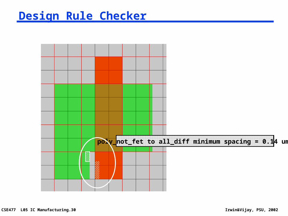
Design Rule Checker
poly_not_fet to all_diff minimum spacing = 0.14 um
CSE477 L05 IC Manufacturing.31 Irwin&Vijay, PSU, 2002
Design Rules
Interface between the circuit designer and process engineer
Guidelines for constructing process masks
Unit dimension: minimum line width scalable design rules: lambda parameter absolute dimensions: micron rules
Rules constructed to ensure that design works even when small fab errors (within some tolerance) occur
A complete set includes set of layers intra-layer: relations between objects in the same layer inter-layer: relations between objects on different layers
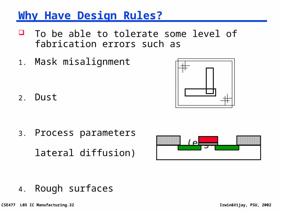
CSE477 L05 IC Manufacturing.32 Irwin&Vijay, PSU, 2002
Why Have Design Rules?
To be able to tolerate some level of fabrication errors such as
1. Mask misalignment
2. Dust
3. Process parameters (e.g., lateral diffusion)
4. Rough surfaces
CSE477 L05 IC Manufacturing.33 Irwin&Vijay, PSU, 2002
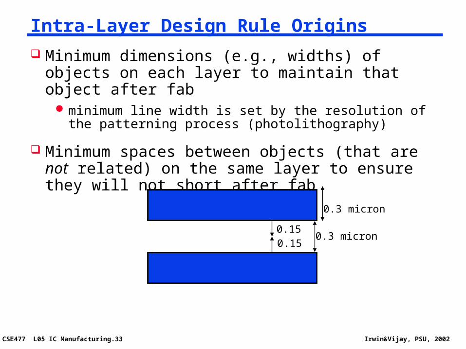
Intra-Layer Design Rule Origins
Minimum dimensions (e.g., widths) of objects on each layer to maintain that object after fab
minimum line width is set by the resolution of the patterning process (photolithography)
Minimum spaces between objects (that are not related) on the same layer to ensure they will not short after fab
0.150.15
0.3 micron
0.3 micron
CSE477 L05 IC Manufacturing.34 Irwin&Vijay, PSU, 2002
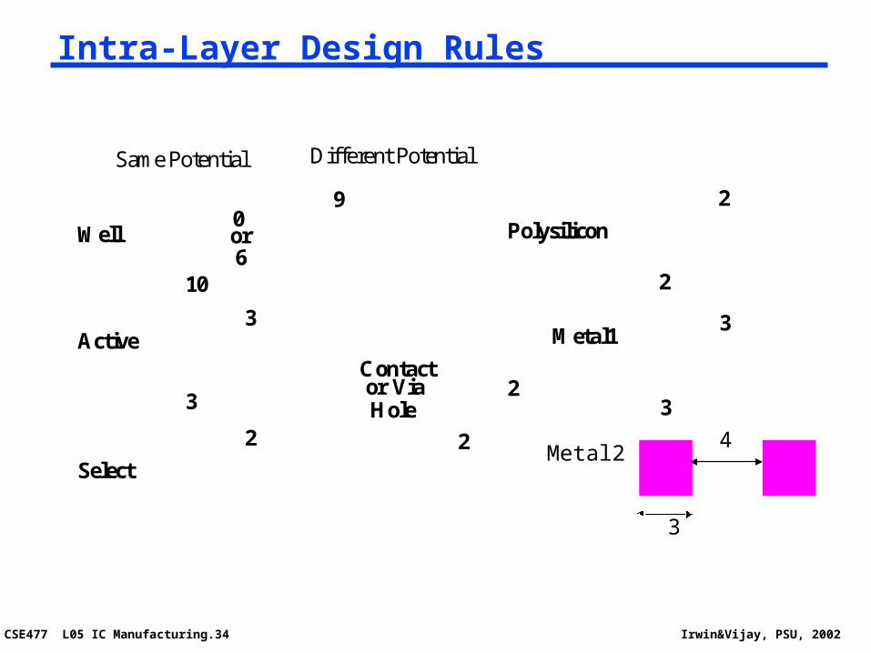
Intra-Layer Design Rules
Metal24
3
10
90
Well
Active3
3
Polysilicon
2
2
Different PotentialSame Potential
Metal13
3
2
Contactor Via
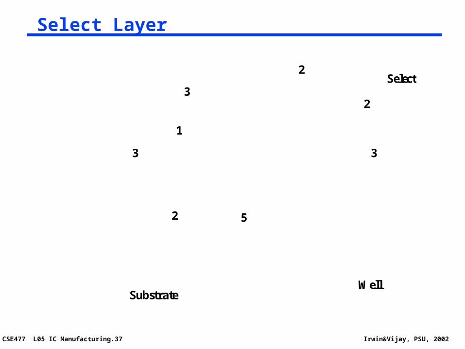
Select
2
or6
2Hole
CSE477 L05 IC Manufacturing.35 Irwin&Vijay, PSU, 2002
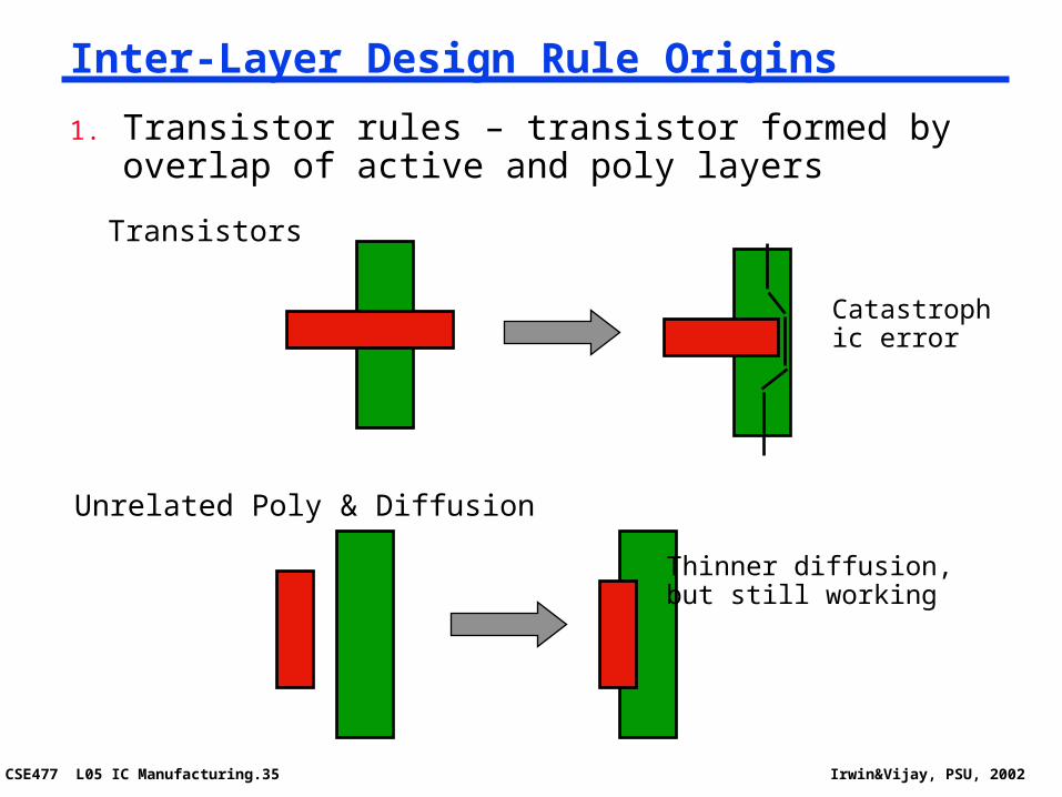
Inter-Layer Design Rule Origins
1. Transistor rules – transistor formed by overlap of active and poly layers
Transistors
Catastrophic error
Unrelated Poly & Diffusion
Thinner diffusion,but still working
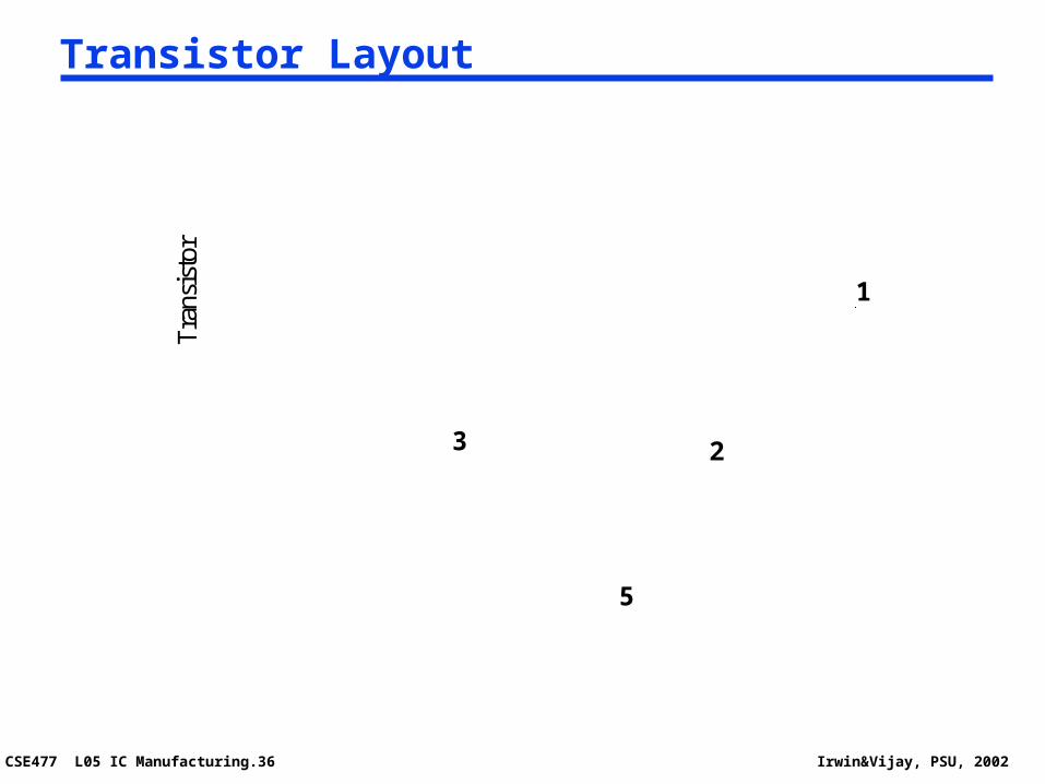
CSE477 L05 IC Manufacturing.36 Irwin&Vijay, PSU, 2002
Transistor Layout
1
2
5
3
Tra
nsis
tor
CSE477 L05 IC Manufacturing.37 Irwin&Vijay, PSU, 2002
Select Layer
1
3 3
2
2
2
WellSubstrate
Select3
5
CSE477 L05 IC Manufacturing.38 Irwin&Vijay, PSU, 2002
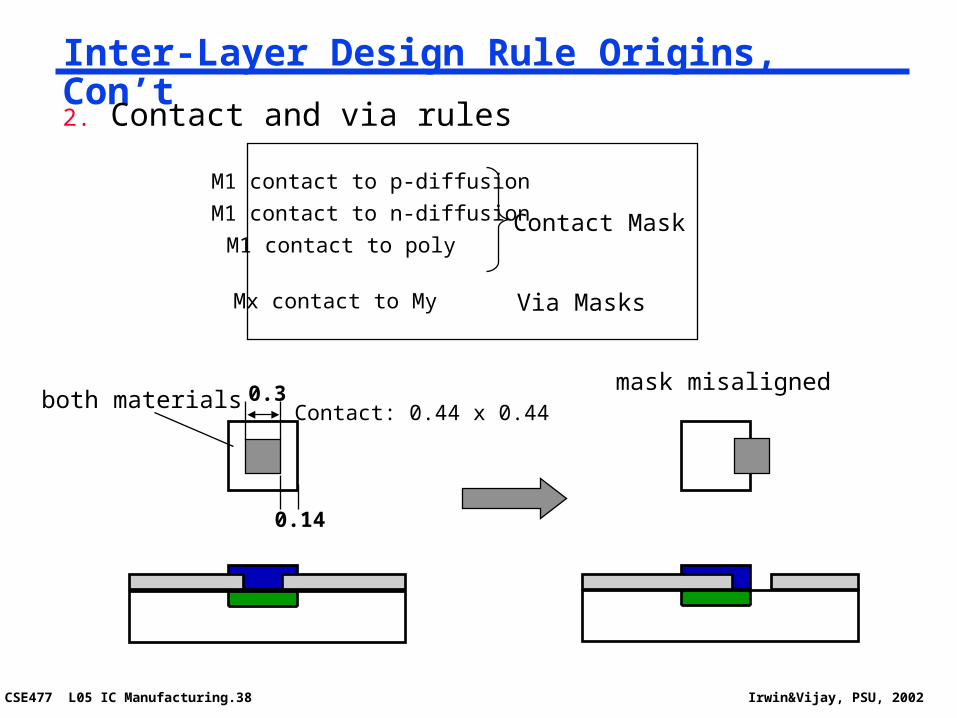
Inter-Layer Design Rule Origins, Con’t
2. Contact and via rules
M1 contact to p-diffusion
M1 contact to poly
Mx contact to My
Contact Mask
Via Masks
0.3
0.14
both materialsmask misaligned
M1 contact to n-diffusion
Contact: 0.44 x 0.44
CSE477 L05 IC Manufacturing.39 Irwin&Vijay, PSU, 2002
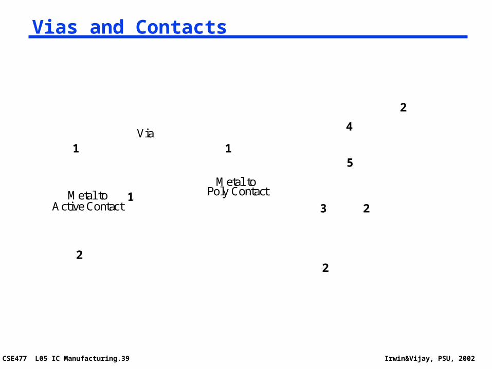
Vias and Contacts
1
2
1
Via
Metal toPoly ContactMetal to
Active Contact
1
2
5
4
3 2
2
CSE477 L05 IC Manufacturing.40 Irwin&Vijay, PSU, 2002
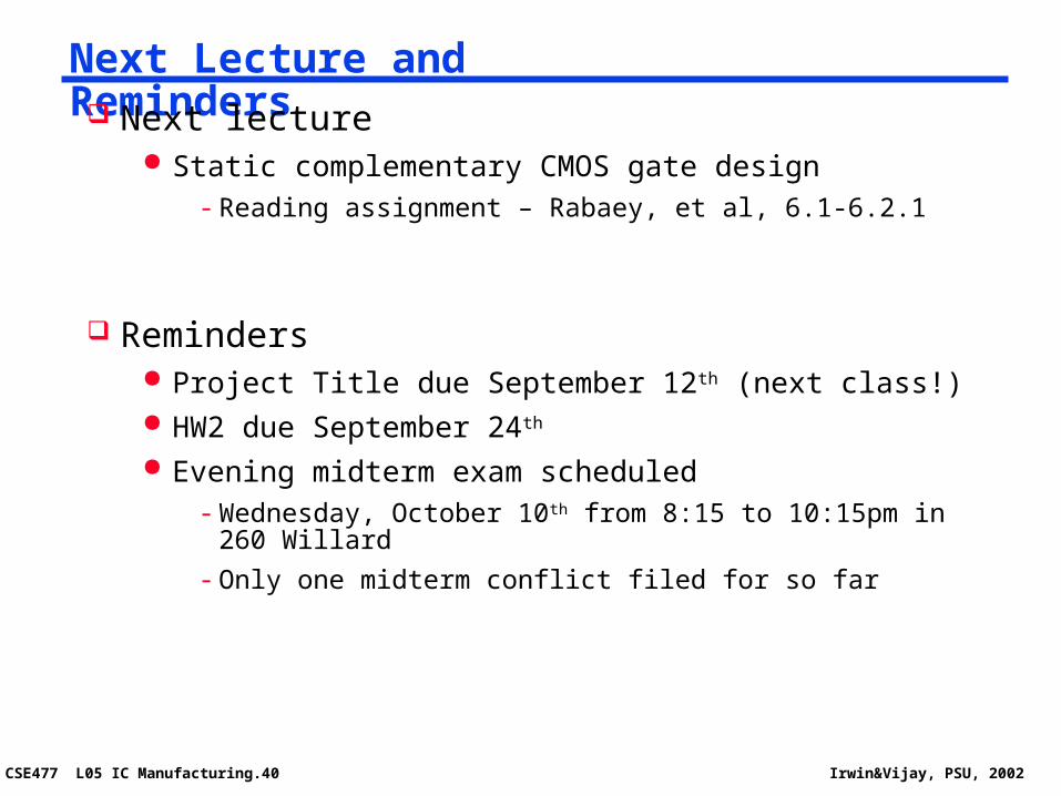
Next Lecture and Reminders Next lecture
Static complementary CMOS gate design- Reading assignment – Rabaey, et al, 6.1-6.2.1
Reminders Project Title due September 12th (next class!) HW2 due September 24th Evening midterm exam scheduled
- Wednesday, October 10th from 8:15 to 10:15pm in 260 Willard
- Only one midterm conflict filed for so far