Embed Size (px)
Citation preview
Solar Energy Materials & Solar Cells 75 (2003) 47–55
Cu(In,Ga)Se2-based thin-film photovoltaicmodules optimized for long-term performance
Johan Wennerberg*, John Kessler, Lars Stolt(Angstr .om Solar Center, Uppsala University, P. O. Box 534, SE-75121 Uppsala, Sweden
Abstract
In this contribution we give an overview of the mechanisms behind degradation of
Cu(In,Ga)Se2-based modules. Based on the results from a detailed analysis of power losses in
modules, prior to and after extended damp heat exposure, we discuss to what extent modules
can be designed to achieve enhanced long-term performance. For conventional modules, we
show that the stability can be improved by optimizing the interconnect and the front contact.
Furthermore, we argue that gridded modules are better from a long-term performance point
of view. A novel interconnect structure, specifically designed for long-term durability, is briefly
discussed. r 2002 Elsevier Science B.V. All rights reserved.
Keywords: Cu(In,Ga)Se2; CIGS; Module design; Stability; Gridded module
1. Background and motivation
Proven long-term stability is an important issue in the context of commercialviability of the Cu(In,Ga)Se2 (CIGS) technology. It is well known that standardizedaccelerated tests of CIGS-based devices often result in severe degradation. Whiledamp heat exposure is known to be harmful to CIGS devices, encapsulated as well asbare, studies on dry heat testing show no or very little impact on performance [1].This indicates that humidity is involved in the mechanisms of the degradationprocess. It is likely to believe that enhanced stability could be achieved by improvingthe encapsulation technology. However, the fact that little is known about thecomplex solid state chemistry of the ZnO:Al/ZnO/CdS/Cu(In,Ga)Se2/Mo/Glassstructure of CIGS devices raises concerns about undesired chemical reactions in the
*Corresponding author. International Science Programme, Uppsala University, Dag Hammarskjolds
vag 31, SE-752 37 Uppsala, Sweden. Tel.: +46-18-471-3577; fax: +46-18-471-3495.
E-mail address: [email protected] (J. Wennerberg).
0927-0248/03/$ - see front matter r 2002 Elsevier Science B.V. All rights reserved.
PII: S 0 9 2 7 - 0 2 4 8 ( 0 2 ) 0 0 1 0 1 - 0
long run [2]. Further understanding of the mechanisms involved in devicedegradation is needed and is becoming increasingly motivated as the CIGStechnology emerges towards large-scale production.In the present work we focus on the mechanisms involved in degradation of CIGS
modules. In this, we quantify degradation of some specific functional parts ofbaseline mini-modules fabricated in our lab at the (Angstr .om Solar Center [3]. A lossanalysis is used in order to determine how the expected degradation of thesefunctional parts will impact device performance. Based on these results, we discuss towhat extend modules can be designed for enhanced long-term performance.
2. Degradation of CIGS devices
Results from accelerated ageing of CIGS devices have been presented previously[4–7]. Here, degradation is enforced by damp heat treatment in conditions similar tothe IEC 1646 Standard (85% relative humidity at 851C). In our test procedure, thedevices are usually tested non-encapsulated. By imposing the already harsh testconditions on naked devices, the test is further accelerated, which will enable us toobserve effects that would possibly not appear for encapsulated devices within thestipulated 1000 h test period. Furthermore, by not encapsulating, we avoid potentialimpact on the devices in terms of mechanical or chemical stress caused by thelaminant that would be irrelevant to the study.The major impact on device performance after extended damp heat exposure is
generally observed in voltage and fill factor. Various interpretations to thesephenomena have been discussed [5,6]. Voltage degradation is said to be dominatedby the effect of enhanced recombination due to increasing defect density in the bulkor at the grain boundaries of the CIGS absorber, and by a shift of the Fermi level atthe CIGS/CdS interface. Furthermore, it has been shown that the concentration offree carriers in the ZnO:Al front contact decreases with damp heat treatment [5].This may impact the fill factor of devices both in terms of higher ohmic losses in thefront contact, and by imposing a shift of the built-in electric field towards then-region, which will increase the electron barrier at the interface [6].When cells are monolithically integrated into modules, additional effects caused
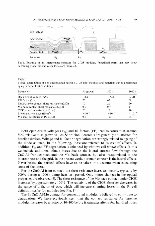
by degradation of interconnects between cells are observed. A cross-sectional view ofa commonly used interconnect structure is presented in Fig. 1, showing somefunctional parts that are of particular importance in the present work.A well-known ageing effect for modules is corrosion of exposed Mo in the P3 cell
isolation scribe, resulting in a detrimental performance loss. Modules have also beenobserved to degrade due to increasing contact resistance of the P2 interconnect viaand by increasing shunting currents in the P1 cell definition scribes. Further detailson interconnect degradation are discussed elsewhere [7].A quantitative view of degradation of non-encapsulated baseline mini-modules is
presented in Table 1. The values are determined from experimental results ofprevious studies on device degradation [5,7], and are here as-grown and after 500 and1000 h of damp heat exposure.
J. Wennerberg et al. / Solar Energy Materials & Solar Cells 75 (2003) 47–5548
Both open circuit voltages (Voc) and fill factors (FF) tend to saturate at around80% relative to as-grown values. Short circuit currents are generally not affected forbaseline devices. Voltage and fill factor degradation are strongly related to ageing ofthe diode as such. In the following, these are referred to as vertical effects. Inaddition, Voc and FF degradation is enhanced by what we call lateral effects. In thiswe include additional ohmic losses due to the lateral current flow through theZnO:Al front contact and the Mo back contact, but also losses related to theinterconnect and the grid. In the present work, our main concern is the lateral effects.Nevertheless, the vertical effects have to be taken into account when calculatingsome of the lateral.For the ZnO:Al front contact, the sheet resistance increases linearly, typically by
200% during a 1000 h damp heat test period. Only minor changes in the opticalproperties are observed [5]. The sheet resistance of the Mo back contact under CIGSincreases by approximately 100%. The resistivity of the CIGS absorber decreases inthe range of a factor of two, which will increase shunting losses in the P1 celldefinition scribe for modules (see Fig. 1).The P2 ZnO:Al/Mo contact for conventional modules is believed to contribute to
degradation. We have previously seen that the contact resistance for baselinemodules increases by a factor of 10–100 before it saturates after a few hundred hours
Fig. 1. Example of an interconnect structure for CIGS modules. Functional parts that may show
degrading properties and cause losses are indicated.
Table 1
Typical degradation of non-encapsulated baseline CIGS mini-modules and materials during accelerated
aging in damp heat conditions
Parameter As-grown 500h 1000 h
Open circuit voltage (mV) B640 B540 B510
Fill factor (%) 75 62 58
ZnO:Al front contact sheet resistance (O/&) 10 20 30
Mo back contact sheet resistance (O/&) 0.5 0.7 1
CIGS absorber resistivity (O cm) 20 10 10
P2 contact resistance (O cm2) B10�4 B10�3 B10�3
Mo sheet resistance in P3 (O/&) 0.5 100 N
J. Wennerberg et al. / Solar Energy Materials & Solar Cells 75 (2003) 47–55 49
of damp heat exposure. Another important lateral effect is corrosion Mo in P3. After500 h of damp heat exposure the sheet resistance of the Mo in P3 has increased by afactor of 100. However, since the scribe is very narrow, only about 50 mm, this haslittle impact on module performance. Not until the back contact has corrodedseverely, which for non-encapsulated devices may last up to 500 h [5], theperformance is drastically reduced.
3. Power loss analysis
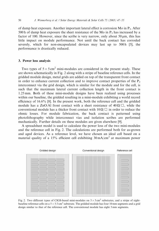
Two types of 5� 5 cm2 mini-modules are considered in the present study. Theseare shown schematically in Fig. 2 along with a stripe of baseline reference cells. In thegridded module design, metal grids are added on top of the transparent front contactin order to enhance current collection and to improve contact properties of the P2interconnect via the grid design, which is similar for the module and for the cell, issuch that the maximum lateral current collection length in the front contact is1.25mm. Both of these mini-module designs have been realized using processeswithin our baseline, the gridded resulting in a mini-module exhibiting a world recordefficiency of 16.6% [8]. In the present work, both the reference cell and the griddedmodule has a ZnO:Al front contact with a sheet resistance of 40O/&, while theconventional module has a thicker front contact with 10O/& in order to reduce theohmic losses. For module fabrication, the back contact is patterned usingphotolithography while interconnect vias and isolation scribes are performedmechanically. Further details on these modules are given elsewhere [9].A spreadsheet model is used to calculate the power loss of the two mini-modules
and the reference cell in Fig. 2. The calculations are performed both for as-grownand aged devices. As a reference level, we have chosen an ideal cell based on amaterial quality of a 15% efficient cell exhibiting 30mA/cm2 at maximum power
Fig. 2. Two different types of CIGS-based mini-modules on 5� 5 cm2 substrates, and a stripe of eight-
baseline reference cells on a 5� 5/3 cm2 substrate. The gridded module has four 10mm segments and a grid
design similar to that of the reference cell. The conventional module has eight 5mm segments.
J. Wennerberg et al. / Solar Energy Materials & Solar Cells 75 (2003) 47–5550
point. This device is ideal in the sense that it has a totally transparent ZnO:Al frontcontact and no ohmic losses. From this reference level, we calculate the additionalpower losses that are caused by optical absorption, parasitic resistances, shunting,dead-area, and shadowing. The losses are calculated for each device at maximumpower point.Ageing is modeled including those device components that will experience lateral
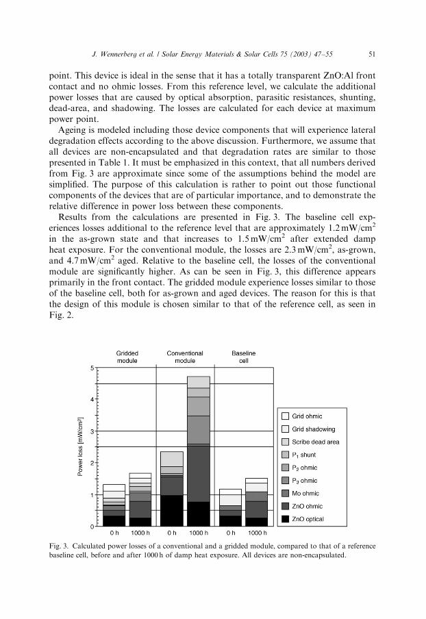
degradation effects according to the above discussion. Furthermore, we assume thatall devices are non-encapsulated and that degradation rates are similar to thosepresented in Table 1. It must be emphasized in this context, that all numbers derivedfrom Fig. 3 are approximate since some of the assumptions behind the model aresimplified. The purpose of this calculation is rather to point out those functionalcomponents of the devices that are of particular importance, and to demonstrate therelative difference in power loss between these components.Results from the calculations are presented in Fig. 3. The baseline cell exp-
eriences losses additional to the reference level that are approximately 1.2mW/cm2
in the as-grown state and that increases to 1.5mW/cm2 after extended dampheat exposure. For the conventional module, the losses are 2.3mW/cm2, as-grown,and 4.7mW/cm2 aged. Relative to the baseline cell, the losses of the conventionalmodule are significantly higher. As can be seen in Fig. 3, this difference appearsprimarily in the front contact. The gridded module experience losses similar to thoseof the baseline cell, both for as-grown and aged devices. The reason for this is thatthe design of this module is chosen similar to that of the reference cell, as seen inFig. 2.
Fig. 3. Calculated power losses of a conventional and a gridded module, compared to that of a reference
baseline cell, before and after 1000 h of damp heat exposure. All devices are non-encapsulated.
J. Wennerberg et al. / Solar Energy Materials & Solar Cells 75 (2003) 47–55 51
Optimizing the front contact is a matter of trading off the optical versus theelectrical properties of the ZnO:Al. Since the current collection length is muchsmaller for the gridded than for the conventional design, the ohmic losses aresmaller. Furthermore, with grids, the module can tolerate a more transparent, i.e. amore resistive ZnO:Al, which reduces the losses caused by optical absorption in thefront contact. As the devices degrade, the ohmic losses of the front contact increases.The changes in optical properties of the front contact are small, but a slightly highertransparency can be observed, which to some extent will reduce the losses caused byoptical absorption. The vertical degradation effects will also have an impact ondevice performance and contribute to the decreasing device efficiency. This is seen ina small reduction of the power losses, since the current at the maximum power pointis reduced.For as-grown CIGS devices, ohmic losses in the Mo back contact constitutes only
a small fraction of the total losses. Nevertheless, it has been observed both for non-encapsulated and laminated modules that the back contact can cause detrimentalperformance loss in the long run. This is caused by corrosion of Mo in the P3 scribe(see Fig. 1). For the power loss calculation we have assumed that necessary actionsare taken in order to suppress P3 corrosion. As can be seen in Fig. 3, the effect onperformance is still significant but not detrimental. This is further discussed in thefollowing section.
4. Improved design
When optimizing the module design for long-term performance, the approach is tominimize the impact from those functional components of the module that can beexpected to contribute significantly to device degradation. In the present work,special attention is paid to the lateral effects, i.e. those caused by degradation of theinterconnect and the transparent front contact.As discussed above, degradation of the ZnO:Al front contact typically appears as
an increasing sheet resistance. For the conventional module, the effect of this onperformance may be reduced by narrowing down the segment width or by modifyingthe ZnO:Al process in order to obtain films with higher conductivity. For the griddedmodule, the ohmic losses in the ZnO:Al can be controlled by varying the spacingbetween the grid fingers. To a first approximation, the spacing can be chosenindependent of segment width. Thus, the gridded design is preferable from a long-term performance point of view. Design of gridded modules is further discussedelsewhere [10].Optimizing the interconnects of the conventional module is a trade-off between
area loss, ohmic losses and shunting. Shunting through the CIGS in the P1 celldefinition scribe (see Fig. 1) is proportional to the cell voltage and inverselyproportional to the width of the scribe and the resistivity of the CIGS. In order tocompensate for the expected increasing shunting losses, as the resistivity decreaseswith time, the width of the P1 scribe should be chosen larger than what is optimal foran as-grown device. This will however impact the active area. At the same time, the
J. Wennerberg et al. / Solar Energy Materials & Solar Cells 75 (2003) 47–5552
expected voltage drop due to vertical cell degradation is actually beneficial from ashunting point of view. Assuming that the gridded module has wider segments thanthe conventional, this design is less sensitive to P1 shunting since the shunted currentis smaller relative to the generated current for each cell.Degrading contact properties of the P2 interconnect via has been previously
discussed [7]. Suggested explanations to this phenomenon are that a resistive oxidelayer is formed between the ZnO:Al and the Mo, or that the ZnO:Al is depleted offree carriers in a thin layer close to the interface. To compensate for the expectedincreasing contact resistance, the P2 scribe can be widened. Gridded modules have ametal-to-metal P2 contact which we presume is more stable. The choice of patterningtechnology is important, in particular for the P3 cell isolation scribe. Mechanicalscribing of P3 often cause severe scratching of the Mo back contact, which is foundto accelerate the corrosion process. Ideally, from an active area point of view, P3should be as thin as possible. This is also beneficial for long-term stability of thedevice since the effect of back-contact corrosion becomes lesser. By using smartpatterning technologies, it is possible to further delay both P2 and P3 degradation.Some aspects on this are briefly discussed in the following section.The general idea behind designing modules for enhanced long-term performance
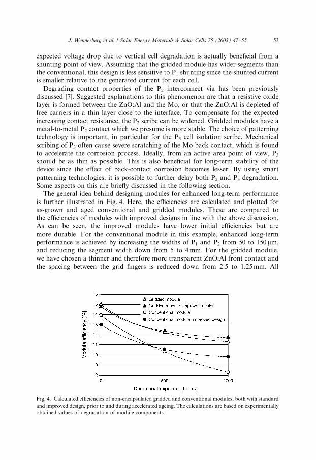
is further illustrated in Fig. 4. Here, the efficiencies are calculated and plotted foras-grown and aged conventional and gridded modules. These are compared tothe efficiencies of modules with improved designs in line with the above discussion.As can be seen, the improved modules have lower initial efficiencies but aremore durable. For the conventional module in this example, enhanced long-termperformance is achieved by increasing the widths of P1 and P2 from 50 to 150 mm,and reducing the segment width down from 5 to 4mm. For the gridded module,we have chosen a thinner and therefore more transparent ZnO:Al front contact andthe spacing between the grid fingers is reduced down from 2.5 to 1.25mm. All
Fig. 4. Calculated efficiencies of non-encapsulated gridded and conventional modules, both with standard
and improved design, prior to and during accelerated ageing. The calculations are based on experimentally
obtained values of degradation of module components.
J. Wennerberg et al. / Solar Energy Materials & Solar Cells 75 (2003) 47–55 53
modules are non-encapsulated and we assume that the corrosion of Mo in P3 issuppressed.
5. Smart patterning
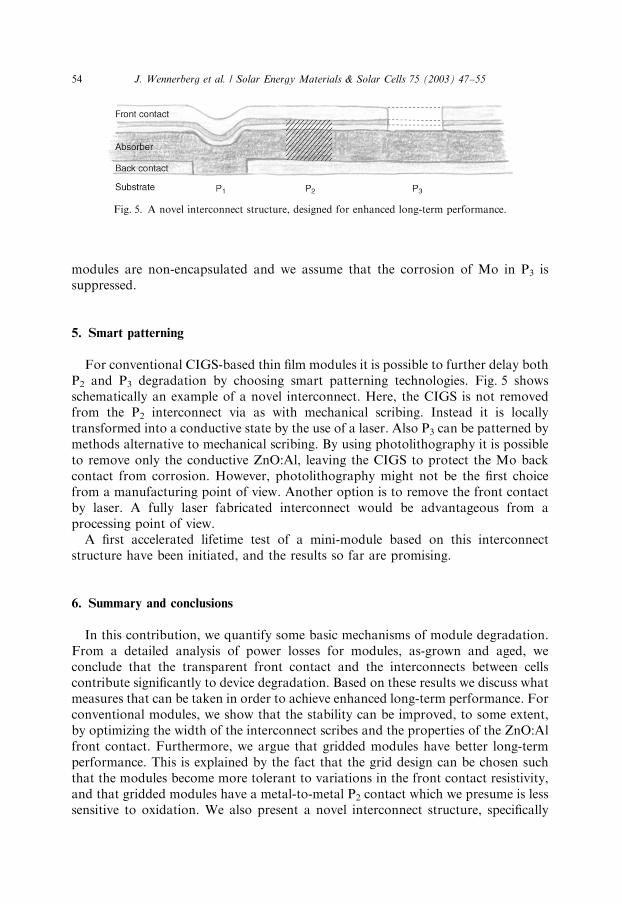
For conventional CIGS-based thin film modules it is possible to further delay bothP2 and P3 degradation by choosing smart patterning technologies. Fig. 5 showsschematically an example of a novel interconnect. Here, the CIGS is not removedfrom the P2 interconnect via as with mechanical scribing. Instead it is locallytransformed into a conductive state by the use of a laser. Also P3 can be patterned bymethods alternative to mechanical scribing. By using photolithography it is possibleto remove only the conductive ZnO:Al, leaving the CIGS to protect the Mo backcontact from corrosion. However, photolithography might not be the first choicefrom a manufacturing point of view. Another option is to remove the front contactby laser. A fully laser fabricated interconnect would be advantageous from aprocessing point of view.A first accelerated lifetime test of a mini-module based on this interconnect
structure have been initiated, and the results so far are promising.
6. Summary and conclusions
In this contribution, we quantify some basic mechanisms of module degradation.From a detailed analysis of power losses for modules, as-grown and aged, weconclude that the transparent front contact and the interconnects between cellscontribute significantly to device degradation. Based on these results we discuss whatmeasures that can be taken in order to achieve enhanced long-term performance. Forconventional modules, we show that the stability can be improved, to some extent,by optimizing the width of the interconnect scribes and the properties of the ZnO:Alfront contact. Furthermore, we argue that gridded modules have better long-termperformance. This is explained by the fact that the grid design can be chosen suchthat the modules become more tolerant to variations in the front contact resistivity,and that gridded modules have a metal-to-metal P2 contact which we presume is lesssensitive to oxidation. We also present a novel interconnect structure, specifically
Fig. 5. A novel interconnect structure, designed for enhanced long-term performance.
J. Wennerberg et al. / Solar Energy Materials & Solar Cells 75 (2003) 47–5554
designed for long-term durability. Initial lifetime testing of a module based on thisinterconnect structure indicates promising results.
Acknowledgements
The authors are greatly thankful to all members of our research team for scientificinput as well as technical support. This work was carried out within the frameworkof the (Angstr .om Solar Center, financially supported by the Foundation for StrategicEnvironmental Research (MISTRA) and the Swedish National Energy Adminis-tration.
References
[1] R.D. Wieting, CIS product introduction: progress and challenges, in: Proceedings of the 15th NCPV
Photovoltaic Progress Review, Denver, AIP Conference Proceeding No. 462, AIP, New york, 1999,
pp. 3–8.
[2] J.-F. Guillemoles, L. Kronik, D. Cahen, U. Rau, A. Jasenek, H.-W. Schock, Stability issues of
Cu(In,Ga)Se2-based solar cells, J. Phys. Chem. B 104 (2000) 4849–4862.
[3] J. Kessler, M. Bodeg(ard, J. Hedstr .om, L. Stolt, Baseline Cu(In,Ga)Se2 device production: control and
statistical significance, Sol. Energy Mater. Sol. Cells 67 (2001) 67–76.
[4] F. Karg, H. Calwer, J. Rimmasch, V. Probst, W. Riedl, W. Stetter, H. Vogt, M. Lampert,
Development of stable thin film solar modules based on CuInSe2, in: Proceedings of the 11th ICTMC,
Salford, 1997.
[5] J. Wennerberg, J. Kessler, L. Stolt, Damp heat testing of high performance CIGS thin film solar cells,
in: Proceedings of the Second World Conference of Photovoltaic Energy Conversion, Vienna, 1998.
[6] M. Schmidt, D. Braunger, R. Sch.affler, H.W. Schock, U. Rau, Influence of damp heat on the
electrical properties of Cu(In,Ga)Se2 solar cells, Thin Solid Films 361–362 (2000) 283–287.
[7] J. Wennerberg, J. Kessler, L. Stolt, Degradation mechanisms of Cu(In,Ga)Se2-based thin film PV
modules, in: Proceedings of the 16th European Photovoltaic Science and Engineering Conference,
Glasgow, 2000, pp. 309–312.
[8] J. Kessler, M. Bodeg(ard, J. Hedstr .om, L. Stolt, New world record Cu(In,Ga)Se2 based mini-modules:
16.6%, in: Proceedings of the 16th European Photovoltaic Science and Engineering Conference,
Glasgow, 2000, pp. 2057–2060.
[9] J. Kessler, J. Wennerberg, M. Bodeg(ard, L. Stolt, High efficiency Cu(In,Ga)Se2 mini-modules, In
Proceedings of the 12th International Photovoltaic Science and Engineering Conference, Cheju
Island, 2001.
[10] J. Wennerberg, J. Kessler, L. Stolt, Design of grided Cu(In,Ga)Se2 thin-film PV modules, Sol. Energy
Mater. Sol. Cells 67 (2001) 59–65.
J. Wennerberg et al. / Solar Energy Materials & Solar Cells 75 (2003) 47–55 55