Embed Size (px)
Citation preview

CUSTOMER APPROVAL SHEET
Company Name
MODEL A080SN03 V0
CUSTOMER APPROVED
Title : Name :
APPROVAL FOR SPECIFICATIONS ONLY (Spec. Ver. ) APPROVAL FOR SPECIFICATIONS AND ES SAMPLE (Spec. Ver. ) APPROVAL FOR SPECIFICATIONS AND CS SAMPLE (Spec. Ver. ) CUSTOMER REMARK :
AUO PM : Valia Hsu P/N : 97.08A10.000 Comment :
1 Li-Hsin Rd. 2. Science-Based Industrial Park Hsinchu 300, Taiwan, R.O.C.
Tel: +886-3-500-8899 Fax: +886-3-577-2730
ALL RIGHTS STRICTLY RESERVED. ANY PORTION OF THIS PAPER SHALL NOT BE REPRODUCED, COPIED, OR TRANSFORMED TO ANY OTHER FORMS WITHOUT PERMISSION FROM AU OPTRONICS CORP.
Doc. version : 1.0 Total pages : 33 Date : 2011/08/24
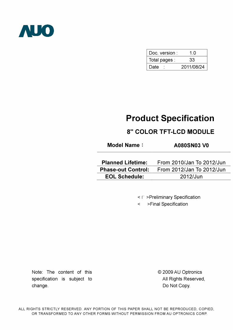
Product Specification 8" COLOR TFT-LCD MODULE
Model Name:::: A080SN03 V0
Planned Lifetime: From 2010/Jan To 2012/Jun Phase-out Control: From 2012/Jan To 2012/Jun
EOL Schedule: 2012/Jun
< >Preliminary Specification < >Final Specification
Note: The content of this specification is subject to change.
© 2009 AU Optronics All Rights Reserved, Do Not Copy.

Version: 1.0
Page: 1/33
ALL RIGHTS STRICTLY RESERVED. ANY PORTION OF THIS PAPER SHALL NOT BE REPRODUCED, COPIED, OR TRANSFORMED TO ANY OTHER FORMS WITHOUT PERMISSION FROM AU OPTRONICS CORP.
Record of Revision Version Revise Date Page Content
0.0 2009/11/25 All First Draft.
0.1 2010/01/07 P3 Modify Panel Power Consumption
P4,5 Modify drawing
P6 Modify Pin Description
P10 Modify DC Charateristics & Current Consumption
P11 Add Gamma voltage & Vcom buffer
P16 Modify Serial Interface Setting Table
P18 Modify Power On/Off Characteristics
P19 Modify Optical Specification
0.2 2010/01/13 P3 Modify Overall Dimension & Weight
P4,5 Modify drawing
0.3 2010/01/15 P3 Revise Backlight Power Consumption
P11,12,19 Revise LED Lightbar current/ Power Consumption
0.4 2010/01/25 P9 Add Input signal voltage
P10 Revise VCOM
P27 Add Application Circuit
0.5 2010/03/10 P11 Add Gamma circuit
P15 Update Parameter description
P16 Update Serial Interface Setting Table
P17 Update Register Description
P31 Add CABC description
0.6 2010/5/12 P10 Add DC Charateristics
P11 Modify Gamma Resistor R83 to 1.05Kohm
P13~P18 Add Input timing remark for Max. value and PWCK setting.
P27 Modify Application Circuit U4 to U3

Version: 1.0
Page: 2/33
ALL RIGHTS STRICTLY RESERVED. ANY PORTION OF THIS PAPER SHALL NOT BE REPRODUCED, COPIED, OR TRANSFORMED TO ANY OTHER FORMS WITHOUT PERMISSION FROM AU OPTRONICS CORP.
0.7 2010/6/22 P.12 Update Gamma voltage suggested circuit
0.8 2011/01/10 P.11 Pull-up/down impedance
P.14 Signal AC Characteristics : Twcl /Twch Symbol definition change
P.10 Delete Operate & Storage Temperature
0.9 2011/6/22 P26 Packing form
1.0 2011/8/24 P.0 Change product lifetime and EOL schedule
Version: 1.0
Page: 3/33
ALL RIGHTS STRICTLY RESERVED. ANY PORTION OF THIS PAPER SHALL NOT BE REPRODUCED, COPIED, OR TRANSFORMED TO ANY OTHER FORMS WITHOUT PERMISSION FROM AU OPTRONICS CORP.
Contents A. General Information..................................................................................................................................... 4 B. Outline Dimension ....................................................................................................................................... 5
1. TFT-LCD Module – Front View.................................................................................................................... 5 2. TFT-LCD Module – Rear View .................................................................................................................... 6
C. Electrical Specifications ............................................................................................................................. 7 1. TFT LCD Panel Pin Assignment ................................................................................................................. 7 2. Backlight Pin Assignment............................................................................................................................ 9 3. Absolute Maximum Ratings......................................................................................................................... 9 4. Electrical DC Characteristics......................................................................................................................11 5. Electrical AC Characteristics ..................................................................................................................... 14 6. Serial Interface Characteristics ................................................................................................................. 16 7. Power On/Off Characteristics.................................................................................................................... 19
D. Optical Specification ................................................................................................................................. 20 E. Reliability Test Items ................................................................................................................................. 23 F. Packing and Marking ................................................................................................................................. 26
1. Packing Form ............................................................................................................................................ 26 2. Module/Panel Label Information ............................................................................................................... 27 3. Carton Label Information........................................................................................................................... 27
G. Application Note ........................................................................................................................................ 28 1. Application Circuit ...................................................................................................................................... 28 2. CABC Description ..................................................................................................................................... 32
H. Precautions ................................................................................................................................................ 33

Version: 1.0
Page: 4/33
ALL RIGHTS STRICTLY RESERVED. ANY PORTION OF THIS PAPER SHALL NOT BE REPRODUCED, COPIED, OR TRANSFORMED TO ANY OTHER FORMS WITHOUT PERMISSION FROM AU OPTRONICS CORP.
A. General Information This product is for portable DVD and digital photo frame application.
NO. Item Unit Specification Remark 1 Screen Size inch 8(Diagonal) 2 Display Resolution dot 800(W)x600RGB(H) 3 Overall Dimension mm 183(W)x141(H)x4.9(D) Note 1 4 Active Area mm 162(W)x121.5(H) 5 Pixel Pitch mm 0.2025(W)x0.2025(H) 6 Color Configuration -- Tri-Gate Note 2 7 Color Depth -- 16.2M Colors Note 3 8 NTSC Ratio % 50 9 Display Mode -- Normally White 10 Panel surface Treatment -- Anti-Glare, 3H 11 Weight g 225 ±10 12 Panel Power Consumption mW 189 Note 4 13 Backlight Power Consumption W 1.58 14 Viewing direction 6 o’clock (gray inversion)
Note 1: Not include blacklight cable and FPC. Refer next page to get further information. Note 2: Below figure shows dot stripe arrangement.
Note 3: The full color display depends on 24-bit data signal (pin 33~40, 42~49, 51~58). Note 4: Please refer to Electrical Characteristics chapter.
…………………….
…………………….
……
…
……
……
……
( 1 2 ….………..……......................... 799 800)
( 1……
……
...……
……
……
…....1800 )
B
G
R
B
G
R
B
G
R
B
G
R
B
G
R
B
G
R
B
G
R
B
G
R

Version: 1.0
Page: 5/33
ALL RIGHTS STRICTLY RESERVED. ANY PORTION OF THIS PAPER SHALL NOT BE REPRODUCED, COPIED, OR TRANSFORMED TO ANY OTHER FORMS WITHOUT PERMISSION FROM AU OPTRONICS CORP.
B. Outline Dimension 1. TFT-LCD Module – Front View

Version: 1.0
Page: 6/33
ALL RIGHTS STRICTLY RESERVED. ANY PORTION OF THIS PAPER SHALL NOT BE REPRODUCED, COPIED, OR TRANSFORMED TO ANY OTHER FORMS WITHOUT PERMISSION FROM AU OPTRONICS CORP.
2. TFT-LCD Module – Rear View
Version: 1.0
Page: 7/33
ALL RIGHTS STRICTLY RESERVED. ANY PORTION OF THIS PAPER SHALL NOT BE REPRODUCED, COPIED, OR TRANSFORMED TO ANY OTHER FORMS WITHOUT PERMISSION FROM AU OPTRONICS CORP.
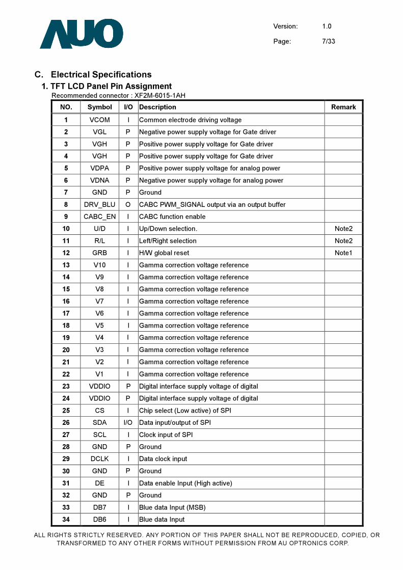
C. Electrical Specifications 1. TFT LCD Panel Pin Assignment
Recommended connector : XF2M-6015-1AH NO. Symbol I/O Description Remark 1 VCOM I Common electrode driving voltage 2 VGL P Negative power supply voltage for Gate driver 3 VGH P Positive power supply voltage for Gate driver 4 VGH P Positive power supply voltage for Gate driver 5 VDPA P Positive power supply voltage for analog power 6 VDNA P Negative power supply voltage for analog power 7 GND P Ground 8 DRV_BLU O CABC PWM_SIGNAL output via an output buffer 9 CABC_EN I CABC function enable 10 U/D I Up/Down selection. Note2 11 R/L I Left/Right selection Note2 12 GRB I H/W global reset Note1 13 V10 I Gamma correction voltage reference 14 V9 I Gamma correction voltage reference 15 V8 I Gamma correction voltage reference 16 V7 I Gamma correction voltage reference 17 V6 I Gamma correction voltage reference 18 V5 I Gamma correction voltage reference 19 V4 I Gamma correction voltage reference 20 V3 I Gamma correction voltage reference 21 V2 I Gamma correction voltage reference 22 V1 I Gamma correction voltage reference 23 VDDIO P Digital interface supply voltage of digital 24 VDDIO P Digital interface supply voltage of digital 25 CS I Chip select (Low active) of SPI 26 SDA I/O Data input/output of SPI 27 SCL I Clock input of SPI 28 GND P Ground 29 DCLK I Data clock input 30 GND P Ground 31 DE I Data enable Input (High active) 32 GND P Ground 33 DB7 I Blue data Input (MSB) 34 DB6 I Blue data Input

Version: 1.0
Page: 8/33
ALL RIGHTS STRICTLY RESERVED. ANY PORTION OF THIS PAPER SHALL NOT BE REPRODUCED, COPIED, OR TRANSFORMED TO ANY OTHER FORMS WITHOUT PERMISSION FROM AU OPTRONICS CORP.
35 DB5 I Blue data Input 36 DB4 I Blue data Input 37 DB3 I Blue data Input 38 DB2 I Blue data Input 39 DB1 I Blue data Input 40 DB0 I Blue data Input (LSB) 41 GND P Ground 42 DG7 I Green data Input (MSB) 43 DG6 I Green data Input 44 DG5 I Green data Input 45 DG4 I Green data Input 46 DG3 I Green data Input 47 DG2 I Green data Input 48 DG1 I Green data Input 49 DG0 I Green data Input (LSB) 50 GND P Ground 51 DR7 I Red data Input (MSB) 52 DR6 I Red data Input 53 DR5 I Red data Input 54 DR4 I Red data Input 55 DR3 I Red data Input 56 DR2 I Red data Input 57 DR1 I Red data Input 58 DR0 I Red data Input (LSB) 59 GND P Ground 60 VCOM I Common electrode driving voltage
I: Input; P: Power
Note1: Global reset, normally pulled high. Suggest to connecting with an RC (R=10K ohm, C=1uF)reset circuit for stability. Normally pull high.
Note2:
U/D Direction L/R Direction H D U H R L L U D L L R

Version: 1.0
Page: 9/33
ALL RIGHTS STRICTLY RESERVED. ANY PORTION OF THIS PAPER SHALL NOT BE REPRODUCED, COPIED, OR TRANSFORMED TO ANY OTHER FORMS WITHOUT PERMISSION FROM AU OPTRONICS CORP.
2. Backlight Pin Assignment Recommended connector : H201K-P02N-02B (MOLEX 51021-0200 COMPATIBLE)
NO. Symbol I/O Description Remark 1 HI I Power supply for backlight unit (High voltage) 2 GND - Ground for backlight unit
3. Absolute Maximum Ratings
Item Symbol Condition Min. Max. Unit Remark VDDIO GND=0 -0.5 5 V VDPA GND=0 -0.5 5.9 V VDNA GND=0 -5.9 0.5 V VGH GND=0 VDPA -- V VGL GND=0 -- VDNA V
Power Voltage
VGH-VGL - 32 V
U
D
R L
U/D=‘L’
U/D=‘H’
L/R=‘H’ L/R=‘L’
Pin1 Pin60

Version: 1.0
Page: 10/33
ALL RIGHTS STRICTLY RESERVED. ANY PORTION OF THIS PAPER SHALL NOT BE REPRODUCED, COPIED, OR TRANSFORMED TO ANY OTHER FORMS WITHOUT PERMISSION FROM AU OPTRONICS CORP.
Vi GND=0 -0.3 VDDIO+0.3 V Note 1 VCOM GND=0 -3.5 0 V V1~V5 GND=0 0 VDPA-0.2 V
Input signal voltage
V6~V10 GND=0 VDNA+0.2 0 V Note 1: DE, Digital Data. Note 2: Functional operation should be restricted under ambient temperature (25). Note 3: Maximum ratings are those values beyond which damages to the device may occur. Functional
operation should be restricted to the limits in the Electrical Characteristics chapter.

Version: 1.0
Page: 11/33
ALL RIGHTS STRICTLY RESERVED. ANY PORTION OF THIS PAPER SHALL NOT BE REPRODUCED, COPIED, OR TRANSFORMED TO ANY OTHER FORMS WITHOUT PERMISSION FROM AU OPTRONICS CORP.
4. Electrical DC Characteristics a. DC Charateristics
Item Symbol Min. Typ. Max. Unit Remark VDDIO 3 3.3 3.6 V VDPA 4.5 5 5.5 V VDNA -5.5 -5 -4.5 V VGH 12.6 14 15.4 V
Power supply
VGL -15.4 -14 -12.6 V VCOM Vcdc -1.6 -1.9 -2.2 V
H Level Vih 0.7xVDDIO -- VDDIO V Input signal voltage L Level Vil 0 -- 0.3xVDDIO V Note 1
Pull-up/down impedance Rin -- 800k -- Input level of V1~V5 Vx GND -- VDPA-0.2 V Note 2
Input level of V6~V10 Vx VDNA+0.2 -- GND V Note 2 Note 1: DE, Digital Data Note 2 : VDPA > V1 > V2 > V3 > V4 > V5 > V6 > V7 > V8 > V9 > V10 > VDNA b. Current Consumption (AGND=GND=0V)
Parameter Symbol Condition Min. Typ. Max. Unit Remark Input current for VDDIO IVDDIO VDDIO=3.3V - 6.45 7 mA Note 1 Input current forVDPA IVDPA VDPA=5V - 5.58 12.9 mA Note 1 Input current for VDNA IVDNA VDNA=-5V - -5.68 -13.4 mA Note 1 Input current for VGH IVGH VGH=14V - 3.96 5 mA Note 1 Inpur current for VGL IVGL VGL=-14V - -4.04 -5 mA Note 1
Input Leakage Current Iin Digital input pins - - ±1 uA Note 2 Note 1: The test pattern use the following pattern.
Note 2: except for pull-up, pull-down pins.

Version: 1.0
Page: 12/33
ALL RIGHTS STRICTLY RESERVED. ANY PORTION OF THIS PAPER SHALL NOT BE REPRODUCED, COPIED, OR TRANSFORMED TO ANY OTHER FORMS WITHOUT PERMISSION FROM AU OPTRONICS CORP.
c. Gamma voltage suggested circuit is as follows V1 4.277
V2 2.882
V3 2.396
V4 1.985
V5 0.994
V6 -0.998
V7 -1.995
V8 -2.409
V9 -2.908
V10 -4.305
Version: 1.0
Page: 13/33
ALL RIGHTS STRICTLY RESERVED. ANY PORTION OF THIS PAPER SHALL NOT BE REPRODUCED, COPIED, OR TRANSFORMED TO ANY OTHER FORMS WITHOUT PERMISSION FROM AU OPTRONICS CORP.
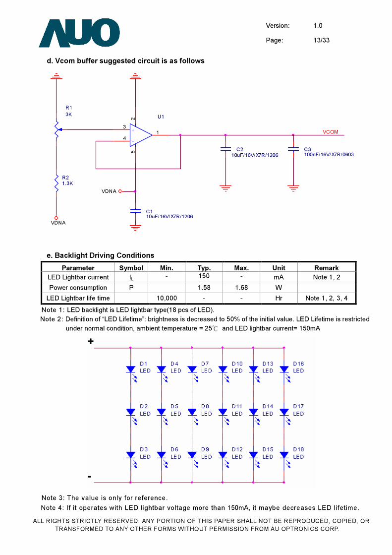
d. Vcom buffer suggested circuit is as follows
3
42
51+
-
U1
C110uF/16V/X7R/1206
R13K
R21.3K
C210uF/16V/X7R/1206
C3100nF/16V/X7R/0603
VDNA
VDNA
VCOM
e. Backlight Driving Conditions
Parameter Symbol Min. Typ. Max. Unit Remark LED Lightbar current IL - 150 - mA Note 1, 2 Power consumption P 1.58 1.68 W
LED Lightbar life time 10,000 - - Hr Note 1, 2, 3, 4 Note 1: LED backlight is LED lightbar type(18 pcs of LED). Note 2: Definition of “LED Lifetime”: brightness is decreased to 50% of the initial value. LED Lifetime is restricted
under normal condition, ambient temperature = 25 and LED lightbar current= 150mA
Note 3: The value is only for reference. Note 4: If it operates with LED lightbar voltage more than 150mA, it maybe decreases LED lifetime.

Version: 1.0
Page: 14/33
ALL RIGHTS STRICTLY RESERVED. ANY PORTION OF THIS PAPER SHALL NOT BE REPRODUCED, COPIED, OR TRANSFORMED TO ANY OTHER FORMS WITHOUT PERMISSION FROM AU OPTRONICS CORP.
5. Electrical AC Characteristics a. Signal AC Characteristics
Parameter Symbol Min. Typ. Max. Unit. Remark Clock High time Twch 8 -- -- ns Clock Low time Twcl 8 -- -- ns Data setup time Tdsu 5 -- -- ns Data hold time Tdhd 10 -- -- ns Data enable set-up time Tesu 4 -- -- ns
b. Input Timing Setting Horizontal timing:
Parameter Symbol Min. Typ. Max. Unit. Remark DCLK frequency Fdclk 36.7 40 45.1 MHz DCLK period Tdclk 22 25 27 ns Hsync period (= Thd + Thbl) Th 986 1056 1183 DCLK Note 1,2 Active Area Thd -- 800 -- DCLK Horizontal blanking Thbl 186 256 383 DCLK

Version: 1.0
Page: 15/33
ALL RIGHTS STRICTLY RESERVED. ANY PORTION OF THIS PAPER SHALL NOT BE REPRODUCED, COPIED, OR TRANSFORMED TO ANY OTHER FORMS WITHOUT PERMISSION FROM AU OPTRONICS CORP.
Horizontal input timing
Vertical timing: Parameter Symbol Min. Typ. Max. Unit. Remark
Vsync period (= Tvd + Tvbl) Tv 620 628 635 Th Active lines Tvd -- 600 -- Th Vertical blanking Tvbl 20 28 35 Th
Vertical timing
Note 1: If input timing operates with Min. to Typ. setting, the PWCK value use default value 1973 (Register R39=0000_0111, Register R40=1011_0101), and no need to change SPI register. Note 2: If input timing operates with Typ. to Max. setting, the PWCK value must be set to 2025(Register R39=0000_0111, Register R40=1110_1001). Please reference the Serial interface setting table in Page.16 to set SPI Register R39 and R40 value.

Version: 1.0
Page: 16/33
ALL RIGHTS STRICTLY RESERVED. ANY PORTION OF THIS PAPER SHALL NOT BE REPRODUCED, COPIED, OR TRANSFORMED TO ANY OTHER FORMS WITHOUT PERMISSION FROM AU OPTRONICS CORP.
6. Serial Interface Characteristics
a. Serial Control Interface AC Characteristic Parameter Symbol Min. Typ. Max. Unit. Remark
Serial clock Tsck 320 -- -- ns SCL pulse duty Tscw 40% 50% 60% Tsck Serial data setup time Tisu 120 -- -- ns Serial data hold time Tihd 120 -- -- ns Serial clock high/low Tssw 120 -- -- ns CS setup time Tcsu 120 -- -- ns CS hold time Tchd 120 -- -- ns Delay from CS to VSYNC Tcv 1 -- -- us Chip select distinguish Tcd 1 -- -- us
AC serial interface write mode timings
b. Register Bank A totally 16-bit register includeing 7-bit address D[15:9], 1-bit Read bit D[8], and 8-bit data D[7:0] can be set via 3-wire serial peripheral interface. Beflow figure is for a detail description of the parameters.

Version: 1.0
Page: 17/33
ALL RIGHTS STRICTLY RESERVED. ANY PORTION OF THIS PAPER SHALL NOT BE REPRODUCED, COPIED, OR TRANSFORMED TO ANY OTHER FORMS WITHOUT PERMISSION FROM AU OPTRONICS CORP.
Figure. Serial interface read sequence
(1) Each serial command consists of 16bits of data which is loaded one bit a time at the rising edge of serial slock SCL. (2) Command loading operation starts from the falling edge of CS and is completed at the next rising edge of CS. (3) The serial control block is operational after power on reset, but commands are established by the following rising edge of End Frame. If command is transferred multiple times for the same resgister, the last command before the following rising edge of the End Frame is valid, except for some special registers (ex. GRB, etc.). (3) If less the 16 bits of SCL are input while CS is low, the transferred data is ignored. The read operation interrupt. (4) If 16 bits or more of SCL are input while CS is low, the first 16 bits of transferred data in the duration of CS=”L” are valid data. (5) Serial block operates with the SCL clock (6) Serial data can be accepted in the standy(power save) mode. (7) It is suggested that DE, DCLK always exists in the same time. (8) When GRB is activated through the serial interface, all register are cleared, except the GRB value. (9) The register setting values are rewritten by the influence of static electricity, a noise, etc. to unsuitable value, incorrect operating may occur. It is suggested that the SPI interface will setup as frequently as possible.
c. Serial Interface Setting Table. ADDRESS R DATA
Reg D15 D14 D13 D12 D11 D10 D9 D8 D7 D6 D5 D4 D3 D2 D1 D0
R0 0 0 0 0 0 0 0 0 -- -- -- 1 note 1 1 note 1 1 note 1 0 1 R1 0 0 0 0 0 0 1 0 0note 1 0 note 1 -- -- 00 00 R39 0 1 0 0 1 1 1 0 -- -- -- -- PW_CK
R40 0 1 0 1 0 0 0 0 PW_CK
Note 1: The value of this bit could not be change. Otherwise the Panel will display abnormal.

Version: 1.0
Page: 18/33
ALL RIGHTS STRICTLY RESERVED. ANY PORTION OF THIS PAPER SHALL NOT BE REPRODUCED, COPIED, OR TRANSFORMED TO ANY OTHER FORMS WITHOUT PERMISSION FROM AU OPTRONICS CORP.
d. Register Description R0 setting Address Bit Discription Default
7 - 2 -- AUO internal use 000111 1 STB Standby mode setting 0 0000000 0 GRB S/W global reset 1
Bit 1 STB
0 Nomal operation (default) 1 Standby mode. Register data are kept.
Bit 0 GRB
0 S/W global reset. Reset all register to default value. H/W GRB has higher priority. 1 Normal operation. (default)
R1 Settings Address Bit Discription Default
7 - 4 -- AUO internal use 0000 3 - 2 CHUD Vertical scan direction setting 00 0000001 1 - 0 CHLR Horizontal scan direction setting 00
Bit 3 - 2 CHUD
0x Accoring to H/W pin U/D setting. (default) 10 Vertical scan direction is from up to down. 11 Vertical scan direction is from down to up.
Bit 1 - 0 CHLR
0x Accoring to H/W pin L/R setting. (default) 10 Horizontal scan direction is from left to right. 11 Horizontal scan direction is from right to left.
R39 setting Address Bit Discription Default
3 - 0 -- AUO PW_CK default value 0111 3 - 0 -- AUO PW_CK Max value 0111 100111
Version: 1.0
Page: 19/33
ALL RIGHTS STRICTLY RESERVED. ANY PORTION OF THIS PAPER SHALL NOT BE REPRODUCED, COPIED, OR TRANSFORMED TO ANY OTHER FORMS WITHOUT PERMISSION FROM AU OPTRONICS CORP.
R40 setting Address Bit Discription Default
7 - 0 -- AUO PW_CK default value 1011_0101 7 - 0 -- AUO PW_CK Max value 1110_1001 101000
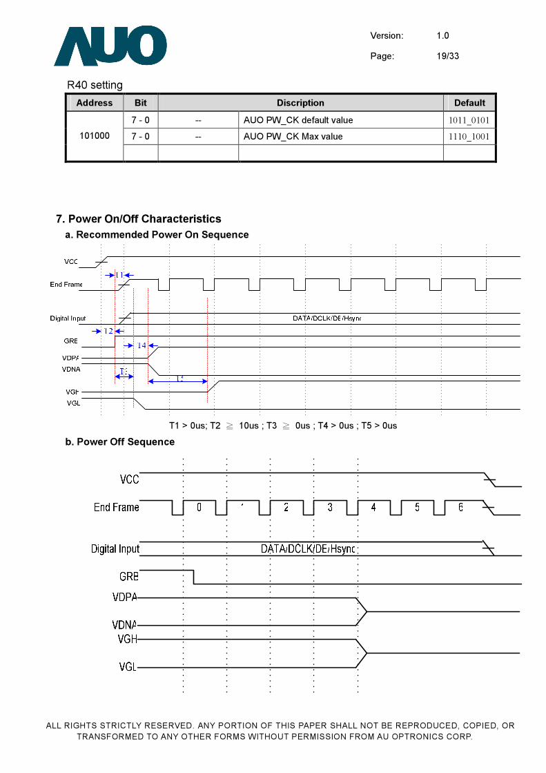
7. Power On/Off Characteristics a. Recommended Power On Sequence
T1 > 0us; T2 ≧ 10us ; T3 ≧ 0us ; T4 > 0us ; T5 > 0us b. Power Off Sequence

Version: 1.0
Page: 20/33
ALL RIGHTS STRICTLY RESERVED. ANY PORTION OF THIS PAPER SHALL NOT BE REPRODUCED, COPIED, OR TRANSFORMED TO ANY OTHER FORMS WITHOUT PERMISSION FROM AU OPTRONICS CORP.
D. Optical Specification All optical specification is measured under typical condition (Note 1, 2)
Item Symbol Condition Min. Typ. Max. Unit Remark Response Time
Rise Fall
Tr Tf
θ=0°
-- --
12 18
24 36
ms ms
Note 3
Contrast ratio CR At optimized viewing angle 400 500 -- Note 4
Top Bottom
Left Viewing Angle
Right
CR≧10
40 50 60 60
60 65 70 70
deg. Note 5
Brightness YL VL = 12V 200 250 -- cd/m2 Note 6 X θ=0° 0.26 0.31 0.36
White Y θ=0° 0.28 0.33 0.38 X θ=0° 0.56 0.61 0.66
Red Y θ=0° 0.30 0.35 0.40 X θ=0° 0.27 0.32 0.37
Green Y θ=0° 0.51 0.56 0.61 X θ=0° 0.10 0.15 0.20
Chromaticity
Blue Y θ=0° 0.07 0.12 0.17
Uniformity ΔYL % 70 75 -- % Note 7 Note 1 : To be measured in the dark room. Ambient temperature =25, and LED lightbar current IL =
150mA. Note 2 :To be measured on the center area of panel with a viewing cone of 1°by Topcon luminance meter
BM-5A, after 15 minutes operation.
CENTER OF THE SCREEN
FIELD=1°
BM-5A

Version: 1.0
Page: 21/33
ALL RIGHTS STRICTLY RESERVED. ANY PORTION OF THIS PAPER SHALL NOT BE REPRODUCED, COPIED, OR TRANSFORMED TO ANY OTHER FORMS WITHOUT PERMISSION FROM AU OPTRONICS CORP.
Note 3: Definition of response time:
The output signals of photo detector are measured when the input signals are changed from “black” to “white”(falling time) and from “white” to “black”(rising time), respectively.
The response time is defined as the time interval between the 10% and 90% of amplitudes. Refer to figure as below.
S ignal( R elat iv e v al ue)
"Black"
Tr Tf
"White""White"
0%10%
90%100%
Note 4.Definition of contrast ratio: Contrast ratio is calculated with the following formula.
status Black"" at is LCD whenoutput detector Photostatus White"" at is LCD whenoutput detector Photo(CR) ratio Contrast =
Note 5. Definition of viewing angle, θ, Refer to figure as below.
X'
yX
y'

Version: 1.0
Page: 22/33
ALL RIGHTS STRICTLY RESERVED. ANY PORTION OF THIS PAPER SHALL NOT BE REPRODUCED, COPIED, OR TRANSFORMED TO ANY OTHER FORMS WITHOUT PERMISSION FROM AU OPTRONICS CORP.
Note 6. Measured at the center area of the panel when all the input terminals of LCD panel are electrically opened.
Note 7: Luminance Uniformity of these 9 points is defined as below:
9)-(1 points 9 in luminance maximum9)-(1 points 9 in luminance minimumUniformity =

Version: 1.0
Page: 23/33
ALL RIGHTS STRICTLY RESERVED. ANY PORTION OF THIS PAPER SHALL NOT BE REPRODUCED, COPIED, OR TRANSFORMED TO ANY OTHER FORMS WITHOUT PERMISSION FROM AU OPTRONICS CORP.
E. Reliability Test Items
No. Test items Conditions Remark 1 High Temperature Storage Ta=70 240Hrs
2 Low Temperature Storage Ta= -30 240Hrs
3 High Ttemperature Operation Tp=60 240Hrs
4 Low Temperature Operation Ta= -10 240Hrs
5 High Temperature & High Humidity Tp= 50.80% RH 240Hrs Operation
6 Heat Shock -10~60,100 cycle, 1Hrs/cycle Non-operation
7 Electrostatic Discharge Contact = ± 4 kV, class B Air = ± 8 kV, class B Note 4
8 Image Sticking 25, 4hrs Note 5 Frequency range : 10~55Hz
Stoke : 1.5mm Sweep : 10 ~ 55 ~ 10Hz
2 hours for each direction of X,Y,Z 9 Vibration
(6 hours for total)
Non-operation JIS C7021, A-10
condition A : 15 minutes
10 Mechanical Shock 100G . 6ms, ±X,±Y,±Z 3 times for each direction
Non-operation JIS C7021,
A-7 condition C
11 Vibration (With Carton) Random vibration:
0.015G2/Hz from 5~200Hz –6dB/Octave from 200~500Hz
IEC 68-34
12 Drop (With Carton) Height: 60cm 1 corner, 3 edges, 6 surfaces
13 Pressure 5kg, 5sec Note 6
Note 1: Ta: Ambient Temperature. Tp: Panel Surface Temperature Note 2: In the standard conditions, there is not display function NG issue occurred. All the cosmetic
specification is judged before the reliability stress. Note 3: All the cosmetic specification is judged before the reliability stress.

Version: 1.0
Page: 24/33
ALL RIGHTS STRICTLY RESERVED. ANY PORTION OF THIS PAPER SHALL NOT BE REPRODUCED, COPIED, OR TRANSFORMED TO ANY OTHER FORMS WITHOUT PERMISSION FROM AU OPTRONICS CORP.
Note4 : All test techniques follow IEC6100-4-2 standard. Test Condition Note
Pattern
Procedure And
Set-up
Contact Discharge:330Ω, 150pF, 1sec, 8 point, 25times/point Air Discharge:330Ω, 150pF, 1sec, 8 point, 25times/point
Criteria B – Some performance degradation allowed. No data lost. Self-recoverable hardware failure.
Others 1. Gun to Panel Distance 2. No SPI command, keep default register settings.
Note 5: Operate with 5×5 chess board pattern as figure and lasting time and temperature as the conditions. Then judge with 50% gray level after waiting 20 min, the mura is less than JND 2.5.
Note 6: The panel is tested as figure. The jig isψ10 mm made by Cu with rubber and the loading speed is 3mm/min on position A~E. After the condition, no glass crack will be found and panel function check is OK.( no guarantee LC mura、LC bubble)
Note 7. In Reliability test, performance is confirmed after leave in room temperature

Version: 1.0
Page: 25/33
ALL RIGHTS STRICTLY RESERVED. ANY PORTION OF THIS PAPER SHALL NOT BE REPRODUCED, COPIED, OR TRANSFORMED TO ANY OTHER FORMS WITHOUT PERMISSION FROM AU OPTRONICS CORP.
Loading
LCM

Version: 1.0
Page: 26/33
ALL RIGHTS STRICTLY RESERVED. ANY PORTION OF THIS PAPER SHALL NOT BE REPRODUCED, COPIED, OR TRANSFORMED TO ANY OTHER FORMS WITHOUT PERMISSION FROM AU OPTRONICS CORP.
F. Packing and Marking 1. Packing Form

Version: 1.0
Page: 27/33
ALL RIGHTS STRICTLY RESERVED. ANY PORTION OF THIS PAPER SHALL NOT BE REPRODUCED, COPIED, OR TRANSFORMED TO ANY OTHER FORMS WITHOUT PERMISSION FROM AU OPTRONICS CORP.
2. Module/Panel Label Information The module/panel (collectively called as the “Product”) will be attached with a label of Shipping Number
which represents the identification of the Product at a specific location. Refer to the Product outline drawing for detailed location and size of the label. The label is composed of a 22-digit serial number and printed with code 39/128 with the following definition:
3. Carton Label Information
The packing carton will be attached with a carton label where packing Q’ty, AUO Model Name, AUO Part Number, Customer Part Number (Optional) and a series of Carton Number in 13 or 14 digits are printed. The Carton Number is apparing in the following format:
Refer to the drawing of packing format for the location and size of the carton label.
Use O
nly / 2
011/8
/30

Version: 1.0
Page: 28/33
ALL RIGHTS STRICTLY RESERVED. ANY PORTION OF THIS PAPER SHALL NOT BE REPRODUCED, COPIED, OR TRANSFORMED TO ANY OTHER FORMS WITHOUT PERMISSION FROM AU OPTRONICS CORP.
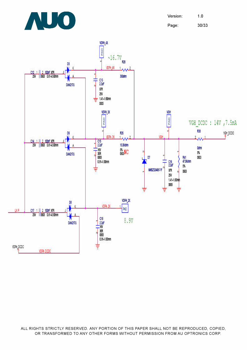
G. Application Note 1. Application Circuit
Use O
nly / 2
011/8
/30

Version: 1.0
Page: 29/33
ALL RIGHTS STRICTLY RESERVED. ANY PORTION OF THIS PAPER SHALL NOT BE REPRODUCED, COPIED, OR TRANSFORMED TO ANY OTHER FORMS WITHOUT PERMISSION FROM AU OPTRONICS CORP.
l Use
Only
/ 201
1/8/30
Version: 1.0
Page: 30/33
ALL RIGHTS STRICTLY RESERVED. ANY PORTION OF THIS PAPER SHALL NOT BE REPRODUCED, COPIED, OR TRANSFORMED TO ANY OTHER FORMS WITHOUT PERMISSION FROM AU OPTRONICS CORP.

Version: 1.0
Page: 31/33
ALL RIGHTS STRICTLY RESERVED. ANY PORTION OF THIS PAPER SHALL NOT BE REPRODUCED, COPIED, OR TRANSFORMED TO ANY OTHER FORMS WITHOUT PERMISSION FROM AU OPTRONICS CORP.

Version: 1.0
Page: 32/33
ALL RIGHTS STRICTLY RESERVED. ANY PORTION OF THIS PAPER SHALL NOT BE REPRODUCED, COPIED, OR TRANSFORMED TO ANY OTHER FORMS WITHOUT PERMISSION FROM AU OPTRONICS CORP.
2. CABC Description

Version: 1.0
Page: 33/33
ALL RIGHTS STRICTLY RESERVED. ANY PORTION OF THIS PAPER SHALL NOT BE REPRODUCED, COPIED, OR TRANSFORMED TO ANY OTHER FORMS WITHOUT PERMISSION FROM AU OPTRONICS CORP.
H. Precautions 1. Do not twist or bend the module and prevent the unsuitable external force for display module during
assembly. 2. Adopt measures for good heat radiation. Be sure to use the module with in the specified temperature. 3. Avoid dust or oil mist during assembly. 4. Follow the correct power sequence while operating. Do not apply the invalid signal, otherwise, it will cause
improper shut down and damage the module. 5. Less EMI: it will be more safety and less noise. 6. Please operate module in suitable temperature. The response time & brightness will drift by different
temperature. 7. Avoid to display the fixed pattern (exclude the white pattern) in a long period, otherwise, it will cause image
sticking. 8. Be sure to turn off the power when connecting or disconnecting the circuit. 9. Polarizer scratches easily, please handle it carefully. 10. Display surface never likes dirt or stains. 11. A dewdrop may lead to destruction. Please wipe off any moisture before using module. 12. Sudden temperature changes cause condensation, and it will cause polarizer damaged. 13. High temperature and humidity may degrade performance. Please do not expose the module to the direct
sunlight and so on. 14. Acetic acid or chlorine compounds are not friends with TFT display module. 15. Static electricity will damage the module, please do not touch the module without any grounded device. 16. Do not disassemble and reassemble the module by self. 17. Be careful do not touch the rear side directly. 18. No strong vibration or shock. It will cause module broken. 19. Storage the modules in suitable environment with regular packing. 20. Be careful of injury from a broken display module. 21. Please avoid the pressure adding to the surface (front or rear side) of modules, because it will cause the
display non-uniformity or other function issue.