Embed Size (px)
Citation preview

Digital PDP Division, LG Electronics Inc.
Product Specification of PDP Module
Revision No. 00 24 / July / 2007 Page 0/36
CUSTOMERAPPROVAL
SPECIFICATION
(●) Preliminary Specification( ) Final Specification
Title PDP60H1#### (60”H1 PDP MODULE)
Signature / Date
Approved by
PDP Engineering DepartmentPDP Division LG Electronics Inc.
Please return 1 copy for our confirmationwith your signature
Approved by
Signature / Date
PART No.
60H1Model Name
LG Electronics Inc.Supplier
PART No.
Model Name
Buyer Name
Digital PDP Division, LG Electronics Inc.
Product Specification of PDP Module
Revision No. 00 24 / July / 2007 Page 1/36
Record of Revisions
Revision No.Effective
DateComments
00 2007.07.24 Establishment
Digital PDP Division, LG Electronics Inc.
Product Specification of PDP Module
Revision No. 00 24 / July / 2007 Page 2/36
0. Warnings and Cautions WARNING indicates hazards that may lead to death or injury if ignored.CAUTION indicates hazards that may lead to injury or damage to property if ignored.
WARNING1) This product uses a high voltage (450 V max.). Do not touch the circuitry of this product with your hands when
power is supplied to the product or immediately after turning off the power. Be sure to confirm that the voltage is dropped to a sufficiently low level.
2) Do not supply a voltage higher than that specified to this product. This may damage the product and may cause a fire.
3) Do not use this product in locations where the humidity is extremely high, where it may be splashed with water, or where flammable materials surround it. Do not install or use the product in a location that does no satisfy the specified environmental conditions. This may damage the product and may cause a fire.
4) If a foreign substance (such as water, metal, or liquid) gets inside the product, immediately turn off the power. Continuing to use the products it may cause fire or electric shock.
5) If the product emits smoke, an abnormal smell, or makes an abnormal sound, immediately turn off the power. If noting is displayed or if the display goes out during use, immediately turn off the power. Continuing to use the product as it is may cause fire or electric shock.
6) Do not disconnect or connect the connector while power to the product is on. It takes some time for the voltage to drop to a sufficiently low level after the power has been turned off. Confirm that the voltage has dropped to a safe level before disconnecting or connecting the connector. Otherwise, this may cause fire, electric shock, or malfunction.
7) Do not pull out or insert the power cable from/to an outlet with wet hands. It may cause electric shock.
8) Do not damage or modify the power cable. It may cause fire or electric shock.
9) If the power cable is damaged, or if the connector is loose, do not use the product; otherwise, this can lead to fire or electric shock.
10) If the power connector or the connector of the power cable becomes dirty or dusty, wipe it with a dry cloth. Otherwise, this can lead to fire.

Digital PDP Division, LG Electronics Inc.
Product Specification of PDP Module
Revision No. 00 24 / July / 2007 Page 3/36
CAUTIONGeneral
• When moving the product, be sure to turn off the power and disconnect all the cables. While moving the product, watch your step. The product may be dropped or fall, leading to injuries of electric shock.
• Do not place this product in a location that is subject to heavy vibration, or on an unstable surface such as an inclined surface. The product may fall off or fall over, causing injuries.
• Before disconnecting cable from the product, be sure to turn off the power. Be sure to hold the connector when disconnecting cables. Pulling a cable with excessive force may cause the core of the cable to be exposed or break the cable, and this can lead to fire or electric shock.
• This product should be moved by two or more persons. If one person attempts to carry this product alone, he/she may be injured.
• This product contains glass. The glass may break, causing injuries, if shock, vibration, heat, or distortion is applied to the product.
• The temperature of the glass surface of the display may rise to 80°C or more depending on the conditions of use. If you touch the glass inadvertently, you may be burned.
• Do not poke or strike the glass surface of the display with a hard object. The glass may break or be scratched. If the glass breaks, you may be injured.
• If you glass surface of the display breaks or is scratched, do not touch the broken pieces or the scratches with bare hands. You may be injured.
• Do not place an object on the glass surface of the display. The glass may break or be scratched.
Design1) This product may be damaged if it is subject to excessive stresses (such as excessive voltage, current, or
temperature). The absolute maximum ratings specify the limits of these stresses, and system design must ensure that none of the absolute maximum ratings are exceeded.
2) Do not use the elements like “Sulfur” that may damage to the PDP Module.
3) The recommended operating conditions are conditions in which the normal operation of this product is guaranteed. All the rated values of the electrical specifications are guaranteed within these conditions. Always use the product within the range of the recommended operating conditions. Otherwise, the reliability of the product may be degraded. Use of the product with a combination of parameters, conditions, or logic not specified in the specifications of this product is not guaranteed. If intending to use the product in such a way, be sure to consult LGE in advance.
4) This product emits near infrared rays (800 to 1000nm) that may cause the remote controllers of other electric products to malfunction. To avoid this, use an infrared absorption filter and thoroughly evaluate the system and environment.

Digital PDP Division, LG Electronics Inc.
Product Specification of PDP Module
Revision No. 00 24 / July / 2007 Page 4/36
Design (continued)4) This product uses high-voltage switching and a high –speed clock. A system using this product should be
designed so that it does not affect the other systems, and should be thoroughly evaluated.
5) This product has a glass display surface. Design your system so that excessive shock and load are not applied to the glass. Exercise care that the vent at the corner of the glass panel is not damaged. If the glass panel or vent is damaged, the product is inoperable.
6) There are some exposed components on the rear panel of this product. Touching these components may cause an electric shock.
7) This product uses a high voltage. Design your system so that any residual voltage in this product is dissipated quickly when power is turned off, observing the specifications.
8) This product uses heat-emitting components. Take the heat emitted by these components into consideration when designing your system. If the product is used outside the specified temperature range, it may malfunction.
9) This product uses a high voltage and, because of its compact design, components are densely mounted on the circuit board. If dust collects on these components, it can cause short-circuiting between the pins of the components and moisture can cause the insulation between the components to break down, causing the product to malfunction.
10) Regulations and standards on safety and electromagnetic interference differ depending on the country. Design your system in compliance with the regulations and standards of the country for which your system is intended.
11) To obtain approval under certain safety standards (such as UL and EN), a filter that passes a shock test must be fitted over the glass surface of the finished product. In addition, it must be confirmed that the level of UV emissions is within the range specified by such standards.
12) If this product is used as a display board to display a static image, “image sticking” occurs. This means that the luminance of areas of the display that remain lit for a long time drops compared with the luminance of areas that are lit for a shorter time, causing uneven luminance across the display. The degree to which this occurs is in proportion to the luminance at which the display is used. To prevent this phenomenon, therefore, avoid static images as much as possible and design your system so that it is used at a low luminance, by reducing signal level difference between bright area and less bright area through signal processing.
13) Within the warranty period, general faults that occur due to defects in components such as ICs will be rectified by LGE without charge. However, IMAGE STICKING is not included in the warranty. Repairs due to the other faults may be charged for depending on responsibility for the faults.
14) In case of AC PDP driving mechanism, Because the brightness of output is not always proportional to input signals. Therefore the non-linearity of gray can occasionally be observed in certain gray levels as well as Contour and Error Diffusion Noise can be appeared when a dark picture is on the screen especially. These are phenomena that can be observed on the PDP driving mechanism. With simple adjustment to picture brightness control, these can be reduced considerably.
15) Because of the need to control the power consumption on the PDP driving mechanism, the APL(Average Picture Level) mode was equipped. Thus, as the picture on the screen changes, there can be slightly switched in brightness. This also is a phenomenon that can be observed on the PDP driving mechanism.
16) This product is designed to LGE’s “Standard” quality grade. If you wish to use the product for applications outside the scope of the “Standard” quality grade, be sure to consult LGE in advance to assess the technological feasibility before starting to design your system.

Digital PDP Division, LG Electronics Inc.
Product Specification of PDP Module
Revision No. 00 24 / July / 2007 Page 5/36
USE1) Because this product uses a high voltage, connecting or disconnecting the connectors while power is supplied to
the product may cause malfunctioning. Never connect or disconnect the connectors while the power is on. Immediately after power has been turned off, a residual voltage remains in the product. Be sure to confirm that the voltage has dropped to a sufficiently low level.
2) Watching the display for a long time can tire the eyes. Take a break at appropriate intervals.
3) PDP ’s brightness and contrast ratio is lower than that of the CRT. The picture is dimmer with surrounding light and better for viewing in dark condition.
4) Do not cover or wrap the product with a cloth or other covering while power is supplied to the product.
5) Before turning on power to the product, check the wiring of the product and confirm that the supply voltage is within the rated voltage range. If the wiring is wrong or if a voltage outside the rated range is applied, the product may malfunction or be damaged.
6) Do not store this product in a location where temperature and humidity are high. This may cause the product to malfunction. Because this product uses a discharge phenomenon, it may take time to light (operation may be delayed) when the product is used after it has been stored for a long time. In this case, it is recommended to light all cells for about 2hours (aging).
7) If the glass surface of the display becomes dirty, wipe it with a soft cloth moistened with a neutral detergent. Do not use acidic or alkaline liquids, or organic solvents.
8) Do not tilt or turn upside down while the module package is carried, the product may be damaged.
9) This product is made from various materials such as glass, metal, and plastic. When discarding it, be sure to contact a professional waste disposal operator.
Repair and MaintenanceBecause this product combines the display panel and driver circuits in a single module, it cannot be repaired or maintained at user’s office or plant. Arrangements for maintenance and repair will be determined later
Others1) If your system requires the user to observe any particular precautions, in addition to the above warnings and
cautions, include such caution and warning statements in the manual for your system.
2) If you have any questions concerning design, such as on housing, storage, or operating environment, consult LGE in advance.

Digital PDP Division, LG Electronics Inc.
Product Specification of PDP Module
Revision No. 00 24 / July / 2007 Page 6/36
1. GENERAL DESCRIPTION
DESCRIPTIONThe PDP60H1#### is a 60-inch 16:9 color plasma display module with resolution of 1920(H)× 1080(V) pixels.This is the display device which offers vivid colors with adopting AC plasma technology by LG Electronics Inc.
FEARURESHigh peak brightness (1000cd/m2 Typical) and high contrast ratio (3000:1 Typical) enables user to create high performance PDP SETs.
APPLICATIONS
Public information displayVideo conference systemsEducation and training systems
Digital PDP Division, LG Electronics Inc.
Product Specification of PDP Module
Revision No. 00 24 / July / 2007 Page 7/36
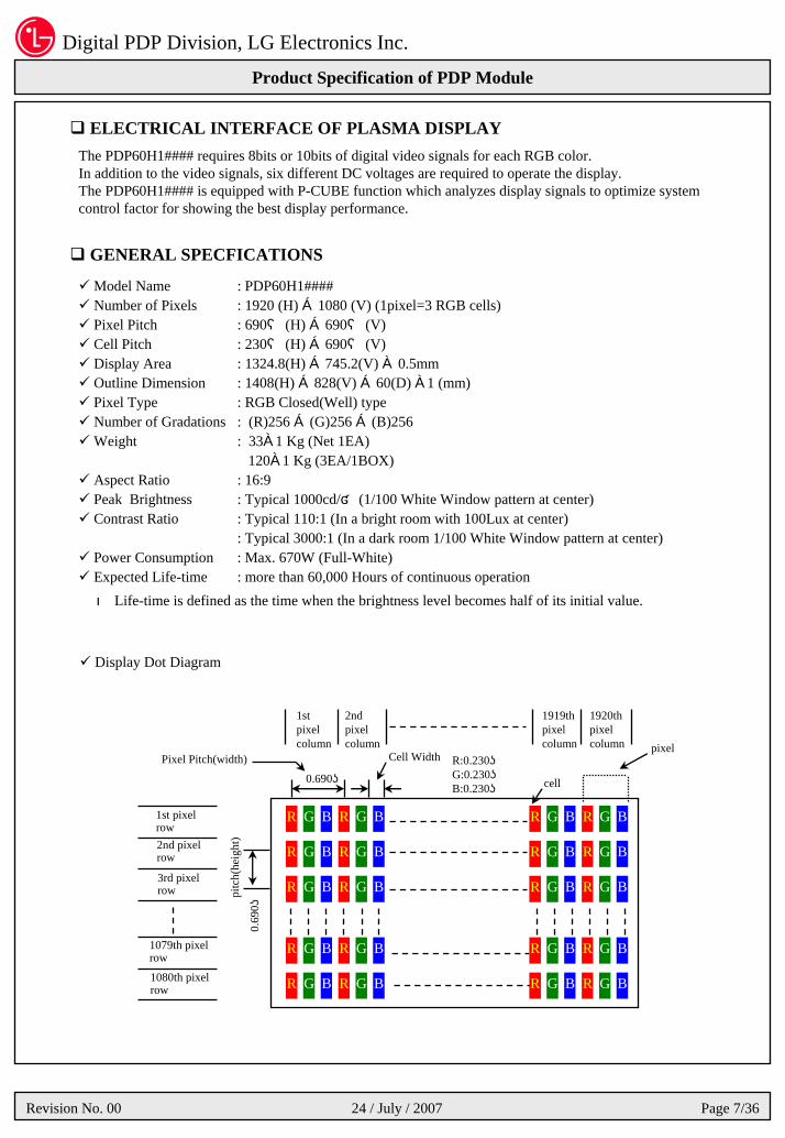
ELECTRICAL INTERFACE OF PLASMA DISPLAYThe PDP60H1#### requires 8bits or 10bits of digital video signals for each RGB color. In addition to the video signals, six different DC voltages are required to operate the display. The PDP60H1#### is equipped with P-CUBE function which analyzes display signals to optimize system control factor for showing the best display performance.
GENERAL SPECFICATIONS
Model NameNumber of PixelsPixel PitchCell PitchDisplay Area Outline Dimension Pixel Type Number of Gradations Weight
Aspect RatioPeak BrightnessContrast Ratio
Power ConsumptionExpected Life-time
: PDP60H1#### : 1920 (H) × 1080 (V) (1pixel=3 RGB cells) : 690㎛ (H) × 690㎛ (V): 230㎛ (H) × 690㎛ (V) : 1324.8(H) × 745.2(V) ± 0.5mm: 1408(H) × 828(V) × 60(D) ±1 (mm) : RGB Closed(Well) type : (R)256 × (G)256 × (B)256 : 33±1 Kg (Net 1EA)
120±1 Kg (3EA/1BOX): 16:9: Typical 1000cd/㎡ (1/100 White Window pattern at center): Typical 110:1 (In a bright room with 100Lux at center): Typical 3000:1 (In a dark room 1/100 White Window pattern at center): Max. 670W (Full-White): more than 60,000 Hours of continuous operation
☞ Life-time is defined as the time when the brightness level becomes half of its initial value.
Display Dot Diagram
2ndpixelcolumn
Pixel Pitch(width) Cell Width
cell
pixel
1stpixelcolumn
1919thpixelcolumn
1920thpixelcolumn
pitc
h(he
ight
)
1st pixelrow2nd pixelrow
3rd pixelrow
1079th pixelrow
1080th pixelrow
R:0.230㎜G:0.230㎜B:0.230㎜
0.690㎜
0.69
0㎜
BGR BGR
BGR BGR
BGR BGR
BGR BGR
BGR BGR
BGR BGR
BGR BGR
BGR BGR
BGR BGR
BGR BGR

Digital PDP Division, LG Electronics Inc.
Product Specification of PDP Module
Revision No. 00 24 / July / 2007 Page 8/36
BLOCK DIAGRAM
Color PDP
1920 X 1080 pixels
Address Driver
Scan
Driv
er
Com
mon sustain driver
Vcc (4.75~5.25V)
Display data, Driver timing
MemoryController
DriverTimingController
Input InterfaceController
Va (55~60V)Vs (185V~195V)
Controller
(External Power)
(LVDS input)
Address Driver
RA1+/ RA1-RB1+/ RB1-RC1+/ RC1-RD1+/ RD1-
RCLK1+/ RCLK1-RE1+/RE1-RA2+/ RA2-RB2+/ RB2-RC2+/ RC2-RD2+/ RD2-
RCLK2+/ RCLK2-RE2+/RE2-
DISPENI2C_SCLK
I2C_SDATA
☞ Applied Voltage level is specified at the time when Full-White pattern is displayed on the panel.
Digital PDP Division, LG Electronics Inc.
Product Specification of PDP Module
Revision No. 00 24 / July / 2007 Page 9/36
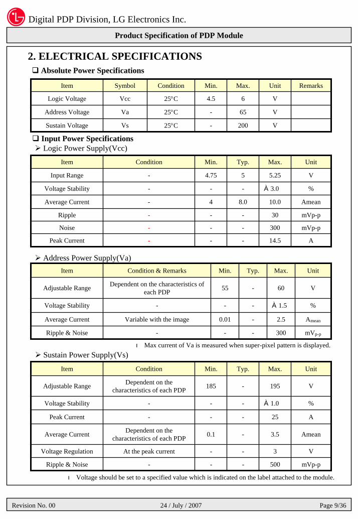
2. ELECTRICAL SPECIFICATIONSAbsolute Power Specifications
Address Power Supply(Va)
Logic Power Supply(Vcc)Input Power Specifications
Item Condition & Remarks Min. Typ. Max. Unit
Adjustable Range Dependent on the characteristics of each PDP 55 - 60 V
Voltage Stability - - - ±1.5 %
Average Current Variable with the image 0.01 - 2.5 Amean
Ripple & Noise - - - 300 mVp-p
Item Condition Min. Typ. Max. Unit
Input Range - 4.75 5 5.25 V
Voltage Stability - - - ±3.0 %
Average Current - 4 8.0 10.0 Amean
Ripple - - - 30 mVp-p
Noise - - - 300 mVp-p
Peak Current - - - 14.5 A
Item Symbol Condition Min. Max. Unit Remarks
Logic Voltage Vcc 25°C
25°C
25°C
4.5 6 V
Address Voltage Va - 65 V
Sustain Voltage Vs - 200 V
Item Condition Min. Typ. Max. Unit
Adjustable Range Dependent on the characteristics of each PDP 185 - 195 V
Voltage Stability - - - ±1.0 %
Peak Current - - - 25 A
Average Current Dependent on the characteristics of each PDP 0.1 - 3.5 Amean
Voltage Regulation At the peak current - - 3 V
Ripple & Noise - - - 500 mVp-p
Sustain Power Supply(Vs)☞Max current of Va is measured when super-pixel pattern is displayed.
☞ Voltage should be set to a specified value which is indicated on the label attached to the module.

Digital PDP Division, LG Electronics Inc.
Product Specification of PDP Module
Revision No. 00 24 / July / 2007 Page 10/36
CONDITIONS OF ACCEPTABILITY
- In order to supply the main power, the manufacturer of end-user products should adopt suitable Main SMPS,
DC/DC Converter which are equipped with OCP and OVP.
- These characteristics of OCP and OVP should be as follows.
Main Power Supply
POINT + 5V Va Vs
OCP 15 Arms 4.0Arms 6.0 Arms
OVP 7 Vrms 72 Vrms 225 Vrms
- OCP ( Over current protection ): This functions to protect power supply or load from output current applied
in excess of limited value.
- OVP ( Over voltage protection): This functions to protect against output voltage exceeding a fixed value and
against over voltage load.
Insulation- The end-user product should satisfy the insulation and material requirements on
Safety Standards of Information Technology Equipment IEC 60950-1, EN 60950-1, UL60950-1 and CSA
C22.2 No60950-1, or IEC 60065, EN 60065, UL 6500 and CSA C22.2 No60065
- The screen filter(Black mask filter) of end-user products should satisfy the supplementary insulation
Additional requirements
- Proper fire enclosure
- Proper mechanical enclosure
- safety test including Power Supply Board should be preformed as a part of the end-user product investigation.

Digital PDP Division, LG Electronics Inc.
Product Specification of PDP Module
Revision No. 00 24 / July / 2007 Page 11/36
Power Supply Sequence
Min. 1 secMin. 2 frameNormal DisplayDISPEN
TVaR
TVsR
TOn
TVaF
TVsF
TOff
Vcc(5V)
Va
Vs
Symbol Description Min. Max. unit
TOnTime interval between 90% of Vcc and 10% of Vs
when Power On1.2 5 sec
TOffTime interval between 10% of Vs and 90% of Vcc
when Power Off20 5000 msec
TVaR Rising Time of Va (10% to 90%) 10 300 msec
TVaF Falling Time of Va (90% to 10%) 50 500 msec
TVsR Rising Time of Vs (10% to 90%) 100 800 msec
TVsF Falling Time of Vs (90% to 10%) 90 500 msec
☞ Vcc should be lower than 0.1V when turn on just after turn off.☞ If power sequence does not meet to above sequence diagram, PDP drivers may be damaged permanently.☞ Even when AC input power supply is switched ON/OFF, above sequence should be observed strictly.

Digital PDP Division, LG Electronics Inc.
Product Specification of PDP Module
Revision No. 00 24 / July / 2007 Page 12/36
LVDS Signal and LVDS Receiver
Definitions and Functions of LVDS SignalDefinition and FunctionSymbol
RA+ Channel-A Pos. Receiver Input
RA- Channel-A Neg. Receiver Input
RB+ Channel-B Pos. Receiver InputRB- Channel-B Neg. Receiver Input
RC+ Channel-C Pos. Receiver Input
RC- Channel-C Neg. Receiver Input
Symbol Definition and FunctionRD+ Channel-A Pos. Receiver Input
RD- Channel-A Neg. Receiver Input
RE+ Channel-B Pos. Receiver InputRE- Channel-B Neg. Receiver Input
RCLK+ Channel-C Pos. Receiver Input
RCLK- Channel-C Neg. Receiver Input
Video Input Connector (P51) Connector type : LG Cable, GT05L-51S-H38
Pin No.Pin No.Pin No. Symbol1 GND2 NC3 NC4 I2C_SCLK5 DISPEN6 I2C_SDATA789
1011 GND12 RA1-13 RA1+14 RB1-15 RB1+16 RC1-17 RC1+
NCNCNCNC
SymbolGNDRCLK1-
18
RCLK1+
19
GND20
RD1-21
RD1+2223242526
RA2-27
RA2+28
RB2-29
RB2+30
RC2-31
RC2+
32
GND
RE1-RE1+GNDGND
3334
Symbol
RCLK2-RCLK2+
35
GND
36
RD2-37
RD2+38
RE2-3940414243
GND
44
GND45
NC46474849
RE2+GNDGNDGND
5051
NCNCNCNC
FI-RE51S-HFK-A 51P connector pin number ( Top view )
1 51
Digital PDP Division, LG Electronics Inc.
Product Specification of PDP Module
Revision No. 00 24 / July / 2007 Page 13/36
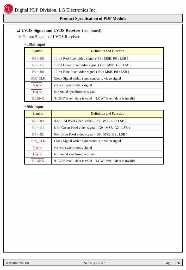
LVDS Signal and LVDS Receiver (continued)Output Signals of LVDS Receiver
Symbol Definition and Function
R9 ~ R0
G9 ~ G0
B9 ~ B0
PIX_CLK
Vsync
Hsync
BLANK
10-bit Red Pixel video signal ( R9 : MSB, R0 : LSB )
10-bit Green Pixel video signal ( G9 : MSB, G0 : LSB )
10-bit Blue Pixel video signal ( B9 : MSB, B0 : LSB )
Clock Signal which synchronous to video signal
vertical synchronous signal
horizontal synchronous signal
‘HIGH’ level : data is valid ‘LOW’ level : data is invalid
• 10bit Input
Symbol Definition and Function
R9 ~ R2
G9 ~ G2
B9 ~ B2
PIX_CLK
Vsync
Hsync
BLANK
8-bit Red Pixel video signal ( R9 : MSB, R2 : LSB )
8-bit Green Pixel video signal ( G9 : MSB, G2 : LSB )
8-bit Blue Pixel video signal ( B9 : MSB, B2 : LSB )
Clock Signal which synchronous to video signal
vertical synchronous signal
horizontal synchronous signal
‘HIGH’ level : data is valid ‘LOW’ level : data is invalid
• 8bit Input
Digital PDP Division, LG Electronics Inc.
Product Specification of PDP Module
Revision No. 00 24 / July / 2007 Page 14/36
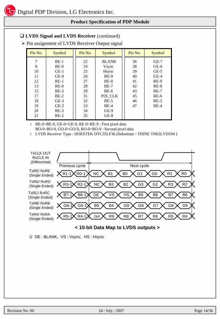
LVDS Signal and LVDS Receiver (continued)Pin assignment of LVDS Receiver Output signal
Pin No. Symbol
78
10111213151718192021
BE-1BE-0GE-1GE-0RE-1RE-0BE-3BE-2GE-3GE-2RE-3RE-2
222425262728293132333435
BLANKVsyncHsyncBE-9BE-8BE-7BE-6
PIX_CLKBE-5BE-4GE-9GE-8
Pin No. Symbol Pin No. Symbol
36383940414243454647
GE-7GE-6GE-5GE-4RE-9RE-8RE-7RE-6RE-5RE-4
☞ BE-0~BE-9, GE-0~GE-9, RE-0~RE-9 : First pixel dataBO-0~BO-9, GO-0~GO-9, RO-0~RO-9 : Second pixel data
☞ LVDS Receiver Type : DOESTEK DTC35LF36 (Substitute : THINE TH63LVD104 )
TxCLK OUTRxCLK IN
(Differential)
< 10-bit Data Map to LVDS outputs >
TxRD/ RxRD(Single Ended)
TxRC/ RxRC(Single Ended) TxRB/ RxRB(Single Ended)
TxRA/ RxRA (Single Ended)
TxRE/ RxRE(Single Ended)
Previous cycle Next cycle
R1-1 R0-1 NC B1 B0 G1 G0 R1 R0
NC B3 B2 G3 G2 R3 R2
DE VS HS B9 B8 B7 B6
B5 B4 G9 G8 G7 G6 G5
G4 R9 R8 R7 R6 R5 R4
R3-1 R2-1
B7-1 B6-1
G6-1 G5-1
R5-1 R4-1
※ DE : BLANK, VS : Vsync, HS : Hsync

Digital PDP Division, LG Electronics Inc.
Product Specification of PDP Module
Revision No. 00 24 / July / 2007 Page 15/36
Input Signal Timing Diagram (Non-interlaced Mode)
Tvsync
Vsync
Hsync
1080+N 1 2 3 - - - 1 2 3 - - - 1080+N 1 2 3 - - -
Tvsync
Vsync
twv
Thsync
thv
Hsync
1080+N 1 2 3 1080
PIX_CLK
(Period of valid data)BLANK
DATA
Thsync
Shaded Area : Invalid
DATAODD
BLANK
PIX_CLK
Hsync
twh tbackph tclk
thb
tch
9601 2
tsud thd
D1 D3 D1919
DATAEVEN D2 D4 D1920
( Period of valid data )
tsubtwclk1 twclk2
tbackpv
1080+N
tvh
thc
twb > 4.6㎲

Digital PDP Division, LG Electronics Inc.
Product Specification of PDP Module
Revision No. 00 24 / July / 2007 Page 16/36
Input Signal Timing Specification
60Hz Mode
No. Symbol Min. Typ. Max. Unit Remark
1
2
3
4
5
6
7
8
9
10
11
12
13
14
Tvsync
t
Thsync
wv
t vh
t hv
t wh
t hc
t ch
t clk
t sub
t hb
t sud
t wclk1
t wclk2
t hd15
㎳ (H)
㎲ (D)
㎲ (D)
㎲ (D)
㎱
㎱
㎱
㎱
㎱
㎱
㎱
㎲ (H)
㎲ (D)
㎲ (H)
㎲ (H)
tclk = twclk1+ twclk2
tsub ≤ thc
t hb ≤ tch
Only for 2-ch input
Pulse width of Hsync
Hsync+ tbph
Horizontal front porch
16.653(1118H)
16.667(1119H)
16.683(1120H)
60 (4H) 74 (5H) 89 (6H)
387(26H) 402(27H) 417(28H)
14.88(1105D) 14.90(1106D) 14.91(1107D)
13.468
3
3
3
3
6.734
6.734
170(12H)
13.417 13.52
0.28(21D) 0.29(22D) 0.31(23D)
1.34(99D) 1.35(100D) 1.37(101D)
0.62(46D)
Pulse width of Vsync
Vsync+ tbpv
Vertical front porch
Period of PIX_CLK73.96MHz~74.530MHz
(vertical back porch)
1H = 14.90㎲
(horizontal back porch)
1frame(typ.) =60Hz
59.94Hz ~ 60.05Hz
☞Min. & Max. of each signal is measured value when other signal is Typ.

Digital PDP Division, LG Electronics Inc.
Product Specification of PDP Module
Revision No. 00 24 / July / 2007 Page 17/36
Input Signal Timing Specification (Continued)
50Hz Mode
No. Symbol Min. Typ. Max. Unit Remark
1
2
3
4
5
6
7
8
9
10
11
12
13
14
Tvsync
t
Thsync
wv
t vh
t hv
t wh
t hc
t ch
t clk
t sub
t hb
t sud
t wclk1
t wclk2
t hd15
㎳ (H)
㎲ (D)
㎲ (D)
㎲ (D)
㎱
㎱
㎱
㎱
㎱
㎱
㎱
㎲ (H)
㎲ (D)
㎲ (H)
㎲ (H)
t clk = t wclk1+ t wclk2
t sub ≤ t hc
t hb ≤ t ch
19.945(1339H)
20.000(1343H)
20.064(1347H)
60 (4H) 74 (5H) 89 (6H)
670 (45H) 685(46H) 700(47H)
14.88(1105D) 14.90(1106D) 14.91(1107D)
13.468
3
3
3
3
6.734
6.734
3230(217H)
0.28(21D) 0.29(22D) 0.31(23D)
1.34(99D) 1.35(100D) 1.37(101D)
0.62(46D)
Only for 2-ch input
13.417 13.52
1frame(typ.) =50Hz
49.85Hz ~ 50.14HzPulse width of Vsync
Vsync+ tbpv(vertical back porch)
Vertical front porch
1H = 14.90㎲
Pulse width of Hsync
Hsync+ tbph(horizontal back porch)
Horizontal front porch
Period of PIX_CLK73.96MHz~74.530MHz
☞Min. & Max. of each signal is measured value when other signal is Typ.

Digital PDP Division, LG Electronics Inc.
Product Specification of PDP Module
Revision No. 00 24 / July / 2007 Page 18/36
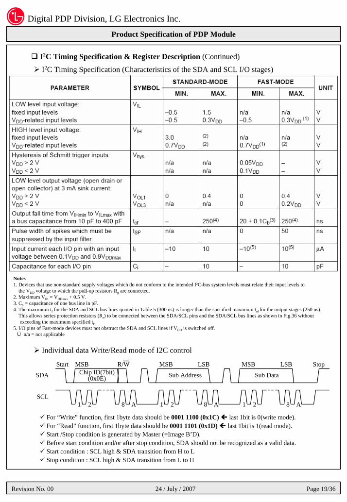
I2C Timing Specification & Register Description
I2C Timing Diagram
I2C Timing Specification (Characteristics of the SDA and SCL bus lines)
Notes1. All values referred to VIHmin and VILmax levels.2. A device must internally provide a hold time of at least 300 ns for the SDA signal (referred to the VIHmin of the SCL signal) to bridge the
undefined region of the falling edge of SCL.3. The maximum tHD;DAT has only to be met if the device does not stretch the LOW period (tLOW) of the SCL signal.4. A Fast-mode I2C-bus device can be used in a Standard-mode I2C-bus system, but the requirement tSU;DAT ≥ 250 ns must then be met.
This will automatically be the case if the device does not stretch the LOW period of the SCL signal.If such a device does stretch the LOW period of the SCL signal, it must output the next data bit to the SDA line tr max + tSU;DAT = 1000 + 250 = 1250 ns (according to the Standard-mode I2C-bus specification) before the SCL line is released.
5. Cb = total capacitance of one bus line in pF. If mixed with Hs-mode devices, faster fall-times according to Table 6 are allowed.※n/a = not applicable
Digital PDP Division, LG Electronics Inc.
Product Specification of PDP Module
Revision No. 00 24 / July / 2007 Page 19/36
I2C Timing Specification & Register Description (Continued)
I2C Timing Specification (Characteristics of the SDA and SCL I/O stages)
For “Write” function, first 1byte data should be 0001 1100 (0x1C) last 1bit is 0(write mode). For “Read” function, first 1byte data should be 0001 1101 (0x1D) last 1bit is 1(read mode). Start /Stop condition is generated by Master (=Image B’D). Before start condition and/or after stop condition, SDA should not be recognized as a valid data.Start condition : SCL high & SDA transition from H to LStop condition : SCL high & SDA transition from L to H
Notes1. Devices that use non-standard supply voltages which do not conform to the intended I2C-bus system levels must relate their input levels to
the VDD voltage to which the pull-up resistors Rp are connected.2. Maximum VIH = VDDmax + 0.5 V.3. Cb = capacitance of one bus line in pF.4. The maximum tf for the SDA and SCL bus lines quoted in Table 5 (300 ns) is longer than the specified maximum tof for the output stages (250 ns).
This allows series protection resistors (Rs) to be connected between the SDA/SCL pins and the SDA/SCL bus lines as shown in Fig.36 without exceeding the maximum specified tf.
5. I/O pins of Fast-mode devices must not obstruct the SDA and SCL lines if VDD is switched off.※ n/a = not applicable
Individual data Write/Read mode of I2C control
Start
Sub Address
MSB R/W MSB LSB Stop
Sub Data
MSB LSB
SDA
1 2 8 A 1 2 8 A 1 2 8 ASCL
Chip ID(7bit)(0x0E)

Digital PDP Division, LG Electronics Inc.
Product Specification of PDP Module
Revision No. 00 24 / July / 2007 Page 20/36
I2C Register Brief Control Signal Register Description
AV/Reserved
RR
11ism_modeRRRR
ISM Mode Registers0x18
R
Gamma Mode Registers0x0B
R R R R
R R R R R R
R
R
1RRR
gamma_mode2(1:0)gamma_mode1(1:0)
scroll_mode(1:0)scroll_
mode_swR
Bw_inv_sw
R
Color Inversion Registers
0x10
Scroll Register
0x11
ps_mode2(2:0)ps_mode1(2:0)R
Power Save Mode Registers0x09
Rbr_mode2(1:0)br_mode1(1:0)
Bright Mode Registers0x08
sync_autoR0x01
Sync Mode Registers
01234567
I2C DataI2C Addr.
hz_select

Digital PDP Division, LG Electronics Inc.
Product Specification of PDP Module
Revision No. 00 24 / July / 2007 Page 21/36
Control Signal Register Description (Continued)
I2C DataI2C Addr.
7 6 5 4 3 2 1 0
0x01 R R R R 1sync
_auto
AV / Reserved
hz
_select
Sync Mode Registers R : Reserved(don’t care)
• sync_auto : Sync automatic/manual mode selection (1 : auto, 0 : manual), Default : Sync_auto• AV mode : AV mode selection (0 : AV, 1 : Reserved)• hz_select : Frequency mode selection (0 : 50Hz, 1 : 60Hz)
Bright Mode Registers
RRBr_mode_60AV
(1:0)Br_mode_50AV
(1:0)0x08
01234567
I2C DataI2C Addr.
R : Reserved(don’t care)
• Br_mode_50AV (1:0) : AV 50Hz Bright mode• Br_mode_60AV (1:0) : AV 60Hz Bright mode
Power Save Mode Registers
• ps_mode_50AV(2:0) : AV 50Hz Power save mode• ps_mode_60AV(2:0) : AV 60Hz Power save mode
ps_mode_60AV(2:0)ps_mode_50AV(2:0)RR0x09
01234567
I2C DataI2C Addr.
R : Reserved(don’t care)
Gamma Mode Registers R : Reserved(don’t care)
RRRRgamma_60AV
(1:0)gamma_50AV
(1:0)0x0B
01234567
I2C DataI2C Addr.
• Gamma_50AV (1:0) : AV 50Hz Gamma mode• Gamma_60AV (1:0) : AV 60Hz Gamma mode
Color Inversion Registers
• Bw_inv_sw : picture Color Inversion (1:ON, 0:OFF)
Bw_inv_swRRRRRRR0x10
01234567
I2C DataI2C Addr.
R : Reserved(don’t care)

Digital PDP Division, LG Electronics Inc.
Product Specification of PDP Module
Revision No. 00 24 / July / 2007 Page 22/36
Control Signal Register Description (Continued)Scroll Registers
I2C DataI2C Addr.
7 6 5 4 3 2 1 0
0x11 R R R R Rscroll_ mode_sw
scroll_mode(1:0)
• scroll_mode_sw : Scroll mode switch (1:ON, 0:OFF)• scroll_mode(1:0) : Scroll mode selection
Scroll_mode [1] : horizontal scroll ON/OFF (1:ON, 0:OFF) Scroll_mode [0] : vertical scroll ON/OFF (1:ON, 0:OFF)
R : Reserved(don’t care)
ISM Mode Registers R : Reserved(don’t care)
11ism_modeRRRRR0x18
01234567
I2C DataI2C Addr.
• ISM_mode : ISM mode switch (1: ON, 0:OFF)

Digital PDP Division, LG Electronics Inc.
Product Specification of PDP Module
Revision No. 00 24 / July / 2007 Page 23/36
Control Signal Register Description (Continued)
Power Save & Brightness Mode
<Power save mode>
000 : normal mode(default)100 : 50% save mode101 : 75% save mode110 : 87.5% save mode111 : linear mode
APL
000 : normal mode110 : 87.5% mode101 : 75% mode100 : 50% mode
111 : linear mode
<Power save mode>Sustainnumber
• Power Save Mode : The power consumption is controlled by varying the sustain number
APL
Sustainnumber 00 : 100% bright mode
01 : 63% bright mode
10 : 40 % bright mode
<Bright mode>
<Bright mode>
00 : 100% bright mode
01 : 63% bright mode
10 : 40 % bright mode
Power saveBright 100% 87.5% 75% 50%
100%
63%
40%
×
× ××
×
×
×
×
- recommended, ×- Don’t use
Digital PDP Division, LG Electronics Inc.
Product Specification of PDP Module
Revision No. 00 24 / July / 2007 Page 24/36
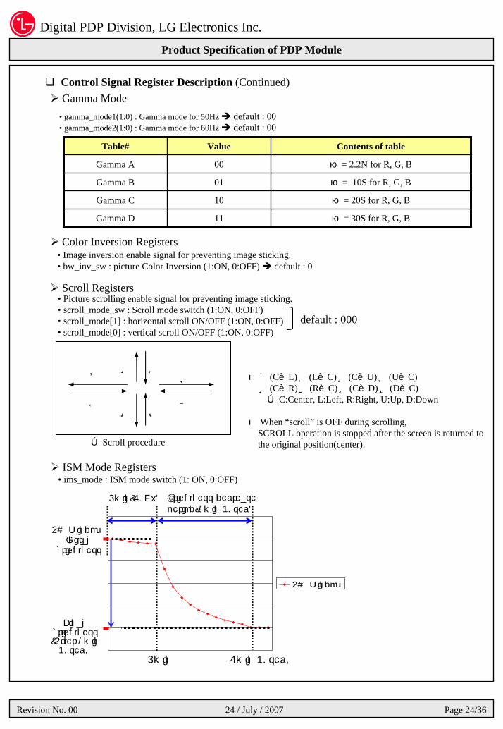
Control Signal Register Description (Continued)Gamma Mode
Table# Value Contents of table
Gamma A
Gamma B
Gamma C
Gamma D
00 Г = 2.2N for R, G, B
01 Г = 10S for R, G, B
10 Г = 20S for R, G, B
11 Г = 30S for R, G, B
• gamma_mode1(1:0) : Gamma mode for 50Hz default : 00• gamma_mode2(1:0) : Gamma mode for 60Hz default : 00
①
②
③ ④⑤
⑥⑦ ⑧
※ Scroll procedure
Color Inversion Registers
Scroll Registers• Picture scrolling enable signal for preventing image sticking.• scroll_mode_sw : Scroll mode switch (1:ON, 0:OFF) • scroll_mode[1] : horizontal scroll ON/OFF (1:ON, 0:OFF) • scroll_mode[0] : vertical scroll ON/OFF (1:ON, 0:OFF)
• Image inversion enable signal for preventing image sticking.• bw_inv_sw : picture Color Inversion (1:ON, 0:OFF) default : 0
default : 000
☞①(C→L) ②(L→C) ③(C→U) ④(U→C) ⑤(C→R) ⑥(R→C) ⑦(C→D) ⑧(D→C) ※ C:Center, L:Left, R:Right, U:Up, D:Down
☞When “scroll” is OFF during scrolling, SCROLL operation is stopped after the screen is returned tothe original position(center).
ISM Mode Registers• ims_mode : ISM mode switch (1: ON, 0:OFF)
4% Window
5min(60Hz) Brightness decreaseperiod(1min 30sec)
4% Window Initial
brightness
Final brightness(After 1min30sec.)
5min 6min 30sec.

Digital PDP Division, LG Electronics Inc.
Product Specification of PDP Module
Revision No. 00 24 / July / 2007 Page 25/36
3. ELECTRO OPTICAL SPECIFICATIONS
Electro Optical characteristic Specifications (60Hz)
ITEM Symbol Condition ☞1) Min Typ Max Unit
Peak White Brightness * BWP 1% white window 500 1,000 - cd/m2 ☞2)
Average White Brightness * BW 100 160 - cd/m2
Brightness Uniformity BU -20 0 +20
X XW 0.280 0.310 0.340White
Y YW 0.280 0.310 0.340
Bright Room
Dark Room☞3)
Brightness Difference Bd Test pattern for Bd - - 30
Color Coordinate Uniformity CU -0.01 Average +0.01
CRBR 100Lx at center 60:1 110:1 -
CRDR 1% white window 1,000:1 3,000:1 -
cd/m2
Power Consumption☞4)
PW Full White - 640 700 W
☞2)ContrastRatio *
ColorCoordinate
Full White
☞*) This data at 50Hz is about 80% level of 60Hz data.☞*) Module temperature can be lowed up to 25% comparing with room temperature when
panel temperature is below than 18 ℃.
☞1) All characteristics are measured in the room temperature after 1 Hour in “Power On” state.☞2) The brightness of the white peak position is measured while the 1%-window pattern is
“ON” state. And then, it should be checked in 10 seconds after 1%-window is “ON” state.The brightness of the black is measured any point(Min. data) of panel.
☞3) The brightness of dark room is less than 1 lux.☞4) Total Power Consumption can be upto 700W according to the displayed pattern.

Digital PDP Division, LG Electronics Inc.
Product Specification of PDP Module
Revision No. 00 24 / July / 2007 Page 26/36
4. MECHANICAL & ENVIRONMENTAL SPECIFICATIONS Mechanical Characteristic Specifications
Item Spec. Unit Remark
Outline Dimensions 1408(H) x 828(V) x 60(D) ±1 mm
Display Area 1324.8(H) X 745.2(V) ±0.5 mm
Net 33±1.0 (1EA) kg
Gross 120±1 (3EA/1BOX) kgWeight
See “Outline Drawing”
Vibration and Drop Specifications
30cm ( Inclined Falling : 20cm)▶ The rest (Front, Backside)
Free falling : 30cm▶ BottomDrop
1.25G, 5 to 55Hz (Sweep time : 2Min.)Y direction , 60 Minutes
▶Non- Operation (3ea Packed state)Vibration
RemarkConditionItem
Recommended Environmental Conditions
0~3000m above the sea level
0~2000m above the sea level
No condensation
700 to 1,100 hPaStorage
10 to 90% RHStorage
-10℃ to 60℃Storage
20 to 80% RHOperationHumidity
Operation
Operation
800 to 1,100 hPaAir Pressure
Panel surface temperature must be kept less than 70 ℃for normal operation.
0℃to 60℃AmbientTemperature
RemarkConditionItem

Digital PDP Division, LG Electronics Inc.
Product Specification of PDP Module
Revision No. 00 24 / July / 2007 Page 27/36
5. IMAGE STICKING CHARACTERISTICS
Image StickingThe fluorescent substance used in the plasma module loses its brightness with the lapse of lighting time. This deterioration in brightness appears to be a difference in brightness in relation to the surroundings, and comes to be recognized as image sticking.
In other words, the image sticking is defined as follows: when the same pattern (of the fixed display) is displayed for a long time, a difference in brightness is caused around the lighting area and non-lighting area due to deterioration in the fluorescent substance.
When the present pattern is changed over to another one, the boundary comes to be seen between the lighting area and non-lighting area due to difference in brightness in the pattern shown shortly before changeover. If this conditions is accumulated, the boundary or image sticking comes to be seen with the naked eyes.
Secular change in brightnessThe life of brightness, defined as the reduction to half the initial level, is more than 25 thousand hours on average.
Conditions: All white (100% white) input at an ambient temperature of 25°C.
However, this lifetime is not a guarantee value for life and brightness. It should be recognized simply as the data for reference.
WarrantyImage sticking and faults in brightness and picture elements are excluded from the warranty objects.
Cause of deterioration in brightnessA major possible cause of deterioration in brightness is damage in the fluorescent substance due to impact caused by ions generated at the time of plasma discharges.
The relationship between integrated lighting time and brightness in this plasma module is described in the attached material. In particular, the deterioration in brightness tends to be accelerated up to 100 hours in the initial period. In the initial period, the fixed display of patterns particularly tends to cause image sticking. The practical value for image sticking is difficult in concrete numerals. As described below, you are advised to take proper measures to make the occurrence of image sticking as slow as possible.
Practical value for Image sticking

Digital PDP Division, LG Electronics Inc.
Product Specification of PDP Module
Revision No. 00 24 / July / 2007 Page 28/36
So long as there is the reduction of brightness in the fluorescent substance, it is impossible to avoid the occurrence of image sticking. Therefore, to relieve image sticking, we offer you a method of entering an image input that may ensure reluctance to the generation of the difference in brightness reduction among the displayed dots.The images from TV broadcasting involve a high rate of motion picture displays. Therefore, there is less chance of being a cause of difference in brightness reduction among the cells. Even when the fixed patterns are displayed, they generally last for a few minutes. Since the same pattern is less liable to be displayed, there is almost no influence toward image sticking.
If the fixed patterns tend to be displayed for a long time, however, there occurs a substantial imbalance between the lighting and non-lighting areas, thus causing a difference in brightness as a result. In this document, we offer you some proposals of installation, paying attentions to the two points: the reduction of difference in brightness achieved by integrated lighting time leveling and the method of edge smearing to make image sticking hard to be discerned.The result from these proposals can, however, greatly depend on the contents of images and the operating environment. Therefore, we consider that it is essential to take the suitable measures in consideration of the customer’s operating environment.
Example of Proposal 1: The display position is moved while the fixed display pattern is changed over, or it is scrolled during the display.Example of Proposal 2: If possible, a pattern of complementary color is incorporated (for integrated time leveling).Example of Proposal 3: The fixed pattern and the motion picture display are reciprocally exchanged, in order to minimize display period of the fixed pattern.Example of Proposal 4: During operation, the brightness of screen is suppressed as low as possible. For the display patterns, characters are indicated not on the black ground (non-picture area) but on the colored ground (mixture of R, G, B recommended).
Proposed measures taken to relieve image sticking

Digital PDP Division, LG Electronics Inc.
Product Specification of PDP Module
Revision No. 00 24 / July / 2007 Page 29/36
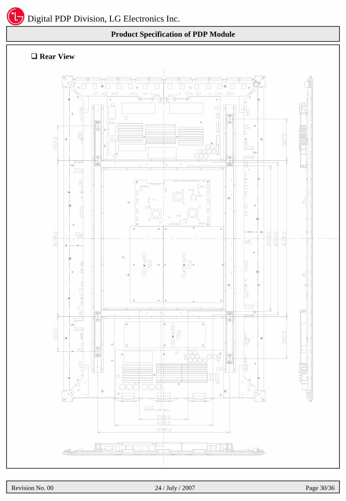
Front View
6. OUTLINE DRAWING
Digital PDP Division, LG Electronics Inc.
Product Specification of PDP Module
Revision No. 00 24 / July / 2007 Page 30/36
Rear View

Digital PDP Division, LG Electronics Inc.
Product Specification of PDP Module
Revision No. 00 24 / July / 2007 Page 31/36
7. CONNECTORS and CONNECTIONS
Power Input Connector
Connector P2002 Pin Assignment (Y SUS Board )
Pin No. Symbol
1
2
3
4
Pin No. Symbol
6
7
8
9
GND
NC
5
GND
Va10
1-1123723-9 Pin numbers(View from the pin connection side)Vs
Vs
GND
GND
Va
Vs123457 68910
Module side connector : 1-1123723-9 (Header)Mating Connector : 1-1123722-9 (Housing)Connector Suppiler : LS Cable
Connector P3001 Pin Assignment ( Y SUS Board )
Pin No. Symbol
1
2
3
4
Pin No. Symbol
6
7
8
9
GND
5
GND
10
+5V GND
+5V
+5V
+5V
+5V
GND
GND
1-1123723-8 Pin numbers(View from the pin connection side)
12345678910
Module side connector : 1-1123723-8 (Header)Mating Connector : 1-1123722-8 (Housing)Connector Suppiler : AMP

Digital PDP Division, LG Electronics Inc.
Product Specification of PDP Module
Revision No. 00 24 / July / 2007 Page 32/36
8. LABEL
LABEL Sticking Position
① IdentificationLabel
③ VoltageLabel
⑤ Module ID
④ ULLabel
②WarningLabel
일치오른쪽 끝
일치왼쪽 끝

Digital PDP Division, LG Electronics Inc.
Product Specification of PDP Module
Revision No. 00 24 / July / 2007 Page 33/36
Identification Label : Label ①
7.0 ㎝
2.5 ㎝
①
②
③
④ ⑤ ⑥
2006.9609K160H1001266.AKLGG AA⑦
60H1####
①Model Name② Bar Code (Code 128, Contains the manufacture No.)③Manufacture No.④ The trade name of LG Electronics⑤Manufactured date (Year & Month)⑥Manufactured place⑦Model Suffix
Warning Label (High Voltage, Hot Surface, Wound) : LABEL ②
18.6 ㎝
2.2 ㎝
① ② ③
①Warning (High Voltage, Hazard Voltage)②Warning (Hot Surface, Hot part can be burn)③ Caution (Wound, Mechanical Hazard)
Digital PDP Division, LG Electronics Inc.
Product Specification of PDP Module
Revision No. 00 24 / July / 2007 Page 34/36
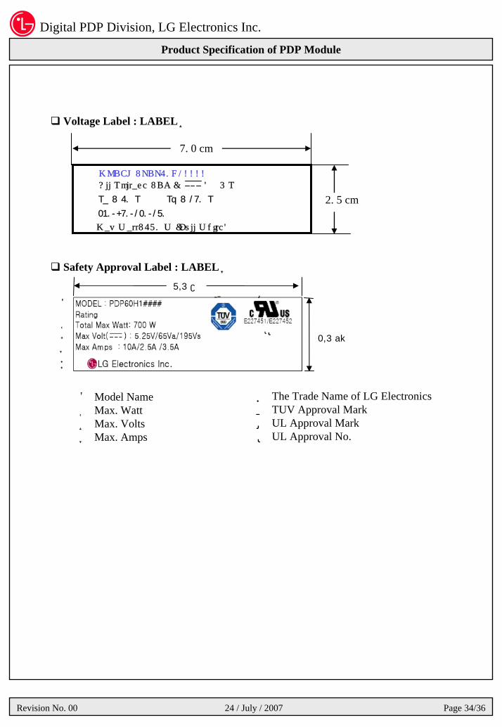
Voltage Label : LABEL ③
7. 0 cm
2. 5 cm
Max Watt: 670 W (Full White)
230/-90/120/170
All Voltage : DC ( ) 5 V
Va : 60 V Vs : 190 V
MODEL : PDP60H1####
Safety Approval Label : LABEL ④
①
②③
⑥ ⑦
⑧
7.5 ㎝
⑤④
⑤
⑥
⑧2.5 cm
①Model Name②Max. Watt ③Max. Volts④Max. Amps
⑤ The Trade Name of LG Electronics⑥ TUV Approval Mark⑦ UL Approval Mark⑧ UL Approval No.

Digital PDP Division, LG Electronics Inc.
Product Specification of PDP Module
Revision No. 00 24 / July / 2007 Page 35/36
9. PACKING
Box packing (3 modules per each Box)
Packing Method
2. Stick the plateon the module
Packing Method
9. BANDING- Stick labelafter banding.
Sequence Sequence
3. Prepare bottombox and bottomEPS 8. Put on the top
box and fold it.
100
70
1. Cover the modulewith conductivebag
4. Packing and insert the module
※ Caution!- Insert rearside first.
7. Insert top EPS .
※ ‘F’ marking side of the top EPS should be laid front(glass) side.
GLASS side of the Module
FRONT
※ Taping as below after foldingthe top BOX.
Transparent tape
Label
Digital PDP Division, LG Electronics Inc.
Product Specification of PDP Module
Revision No. 00 24 / July / 2007 Page 36/36
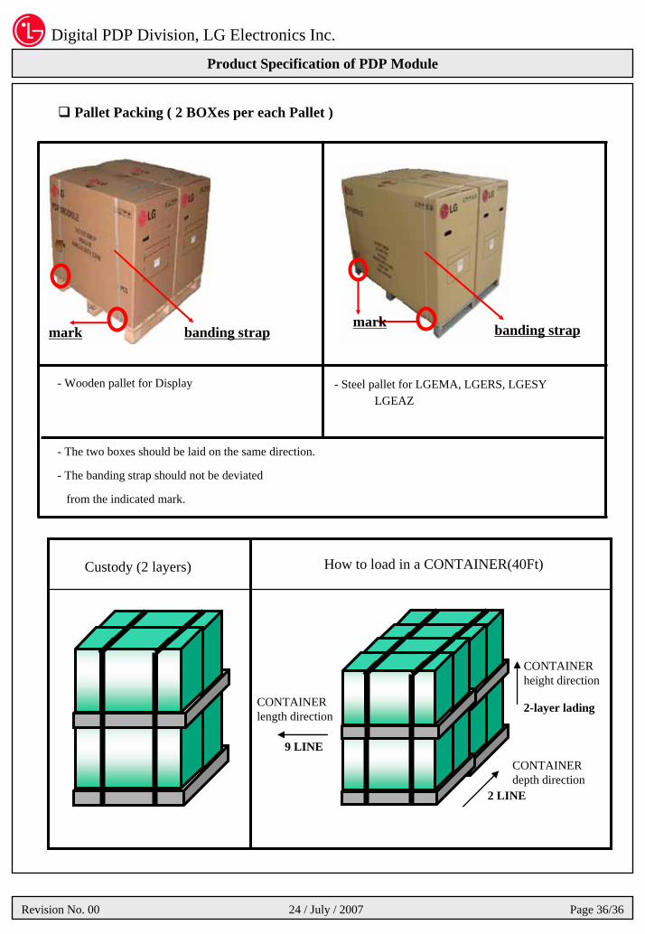
Pallet Packing ( 2 BOXes per each Pallet )
mark banding strap
- The two boxes should be laid on the same direction.
- The banding strap should not be deviated
from the indicated mark.
mark banding strap
- Wooden pallet for Display - Steel pallet for LGEMA, LGERS, LGESY LGEAZ
How to load in a CONTAINER(40Ft)
CONTAINERlength direction
9 LINECONTAINERdepth direction
2 LINE
CONTAINERheight direction
2-layer lading
Custody (2 layers)