Embed Size (px)
Citation preview
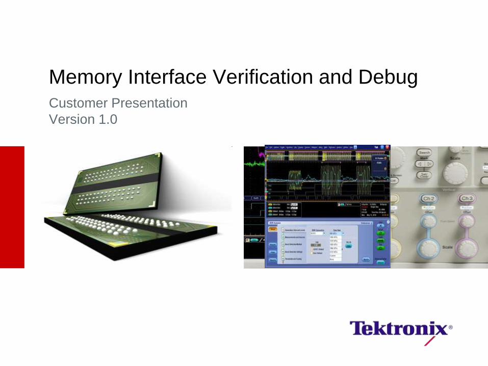
Memory Interface Verification and Debug Customer Presentation
Version 1.0
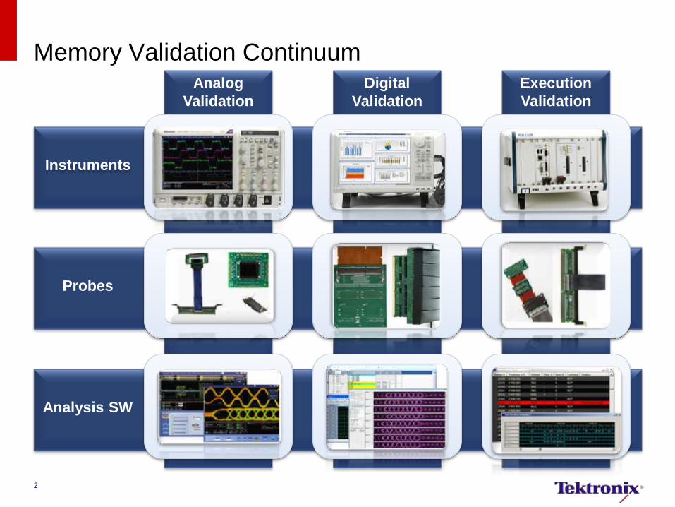
Memory Validation Continuum
Analysis SW
Analog
Validation
Instruments
Probes
2
Digital
Validation
Execution
Validation
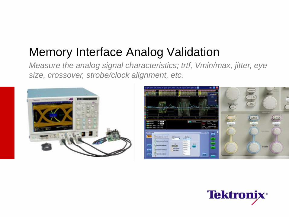
Memory Interface Analog Validation Measure the analog signal characteristics; trtf, Vmin/max, jitter, eye
size, crossover, strobe/clock alignment, etc.
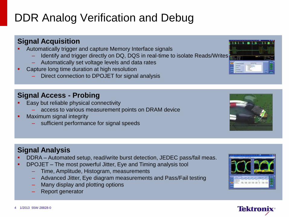
DDR Analog Verification and Debug
Signal Access - Probing Easy but reliable physical connectivity
‒ access to various measurement points on DRAM device
Maximum signal integrity
‒ sufficient performance for signal speeds
Signal Acquisition Automatically trigger and capture Memory Interface signals
‒ Identify and trigger directly on DQ, DQS in real-time to isolate Reads/Writes
‒ Automatically set voltage levels and data rates
Capture long time duration at high resolution
‒ Direct connection to DPOJET for signal analysis
Signal Analysis DDRA – Automated setup, read/write burst detection, JEDEC pass/fail meas.
DPOJET – The most powerful Jitter, Eye and Timing analysis tool
‒ Time, Amplitude, Histogram, measurements
‒ Advanced Jitter, Eye diagram measurements and Pass/Fail testing
‒ Many display and plotting options
‒ Report generator
4 1/2013 55W-28828-0
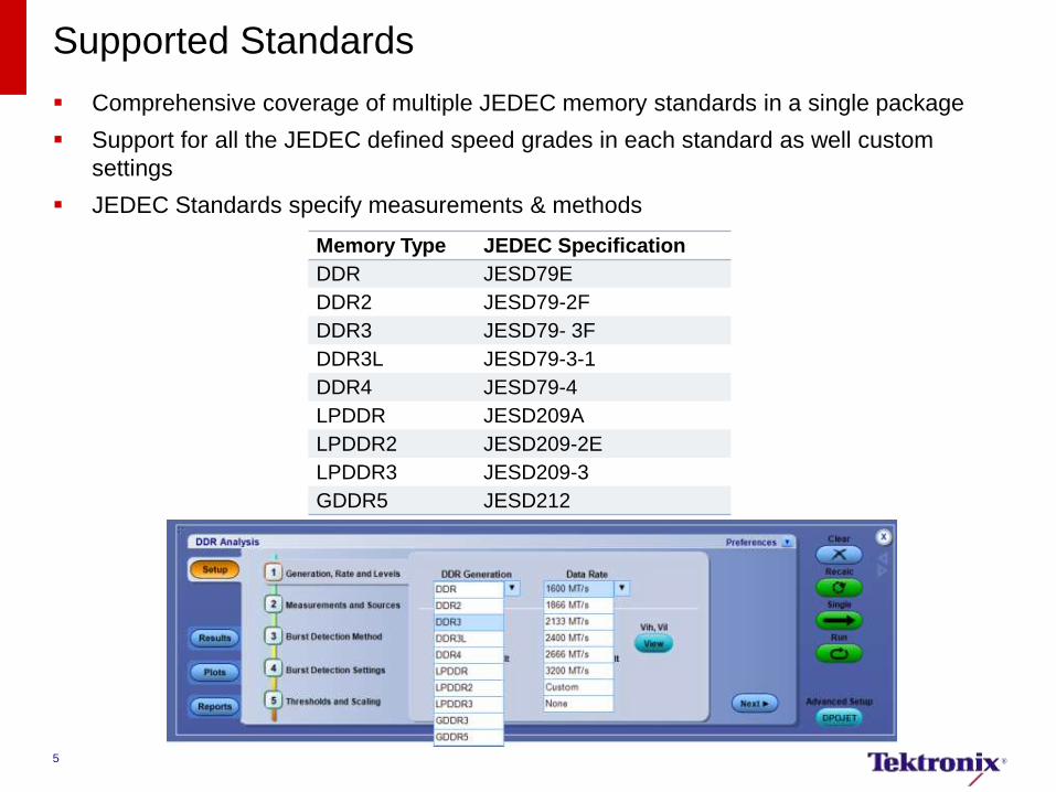
Supported Standards Comprehensive coverage of multiple JEDEC memory standards in a single package
Support for all the JEDEC defined speed grades in each standard as well custom
settings
JEDEC Standards specify measurements & methods
Memory Type JEDEC Specification
DDR JESD79E
DDR2 JESD79-2F
DDR3 JESD79- 3F
DDR3L JESD79-3-1
DDR4 JESD79-4
LPDDR JESD209A
LPDDR2 JESD209-2E
LPDDR3 JESD209-3
GDDR5 JESD212
5
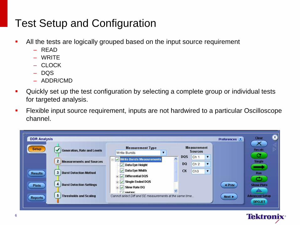
Test Setup and Configuration
All the tests are logically grouped based on the input source requirement
– READ
– WRITE
– CLOCK
– DQS
– ADDR/CMD
Quickly set up the test configuration by selecting a complete group or individual tests
for targeted analysis.
Flexible input source requirement, inputs are not hardwired to a particular Oscilloscope
channel.
6
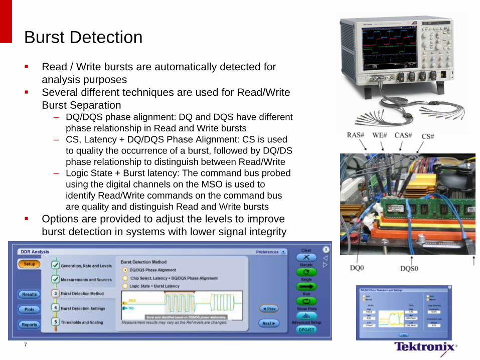
Burst Detection
Read / Write bursts are automatically detected for
analysis purposes
Several different techniques are used for Read/Write
Burst Separation – DQ/DQS phase alignment: DQ and DQS have different
phase relationship in Read and Write bursts
– CS, Latency + DQ/DQS Phase Alignment: CS is used
to quality the occurrence of a burst, followed by DQ/DS
phase relationship to distinguish between Read/Write
– Logic State + Burst latency: The command bus probed
using the digital channels on the MSO is used to
identify Read/Write commands on the command bus
are quality and distinguish Read and Write bursts
Options are provided to adjust the levels to improve
burst detection in systems with lower signal integrity
7
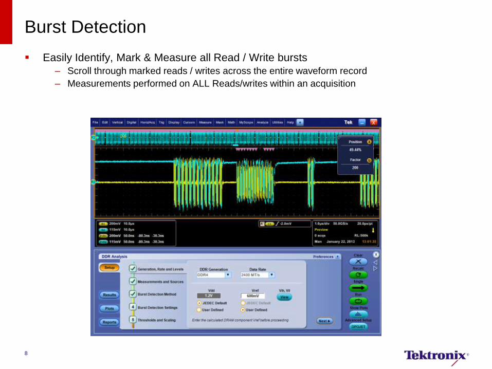
Burst Detection
Easily Identify, Mark & Measure all Read / Write bursts
– Scroll through marked reads / writes across the entire waveform record
– Measurements performed on ALL Reads/writes within an acquisition
8
9
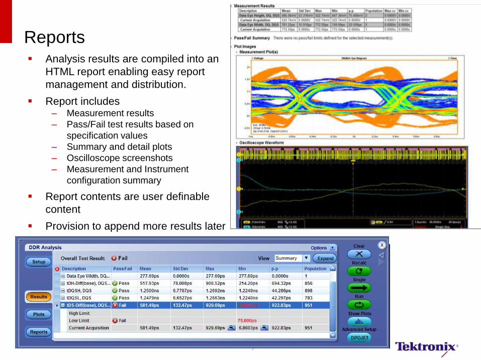
Reports Analysis results are compiled into an
HTML report enabling easy report
management and distribution.
Report includes – Measurement results
– Pass/Fail test results based on
specification values
– Summary and detail plots
– Oscilloscope screenshots
– Measurement and Instrument
configuration summary
Report contents are user definable
content
Provision to append more results later
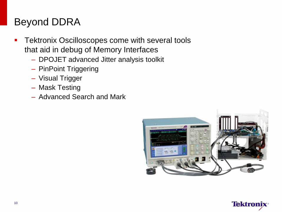
Beyond DDRA
Tektronix Oscilloscopes come with several tools
that aid in debug of Memory Interfaces
– DPOJET advanced Jitter analysis toolkit
– PinPoint Triggering
– Visual Trigger
– Mask Testing
– Advanced Search and Mark
10
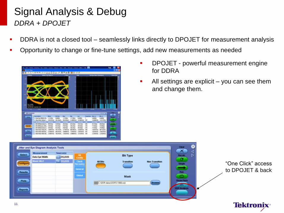
Signal Analysis & Debug DDRA + DPOJET
DDRA is not a closed tool – seamlessly links directly to DPOJET for measurement analysis
Opportunity to change or fine-tune settings, add new measurements as needed
“One Click” access
to DPOJET & back
DPOJET - powerful measurement engine
for DDRA
All settings are explicit – you can see them
and change them.
11
12
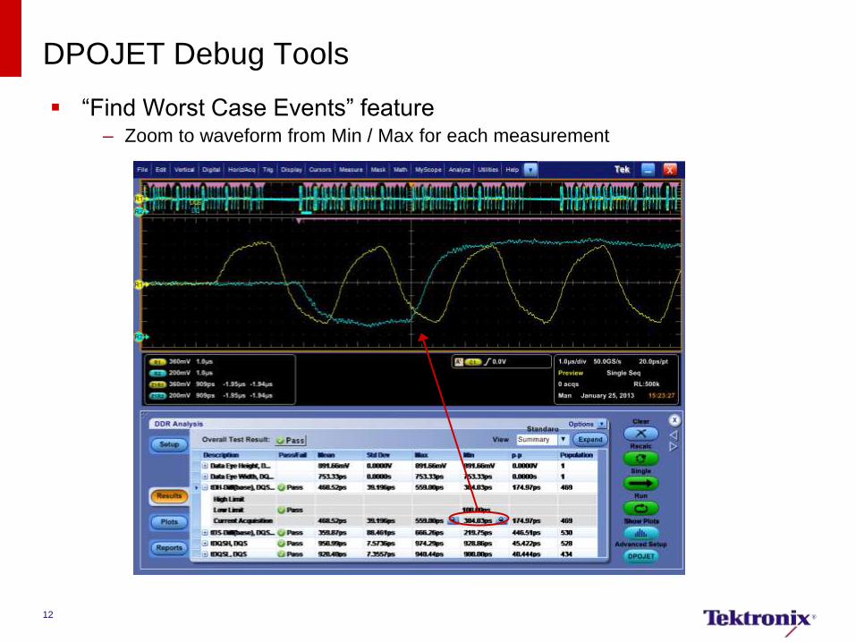
DPOJET Debug Tools
“Find Worst Case Events” feature – Zoom to waveform from Min / Max for each measurement
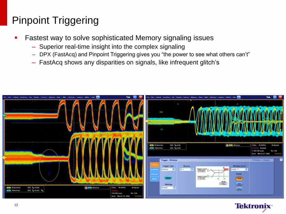
Pinpoint Triggering
Fastest way to solve sophisticated Memory signaling issues
– Superior real-time insight into the complex signaling
– DPX (FastAcq) and Pinpoint Triggering gives you “the power to see what others can’t”
– FastAcq shows any disparities on signals, like infrequent glitch’s
13
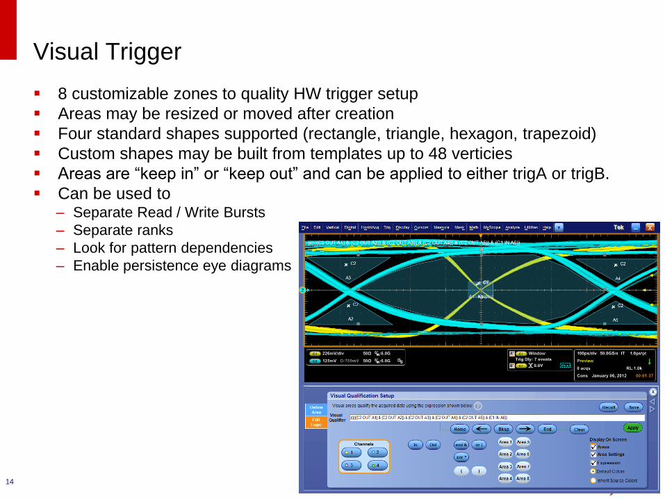
Visual Trigger
8 customizable zones to quality HW trigger setup
Areas may be resized or moved after creation
Four standard shapes supported (rectangle, triangle, hexagon, trapezoid)
Custom shapes may be built from templates up to 48 verticies
Areas are “keep in” or “keep out” and can be applied to either trigA or trigB.
Can be used to – Separate Read / Write Bursts
– Separate ranks
– Look for pattern dependencies
– Enable persistence eye diagrams
14
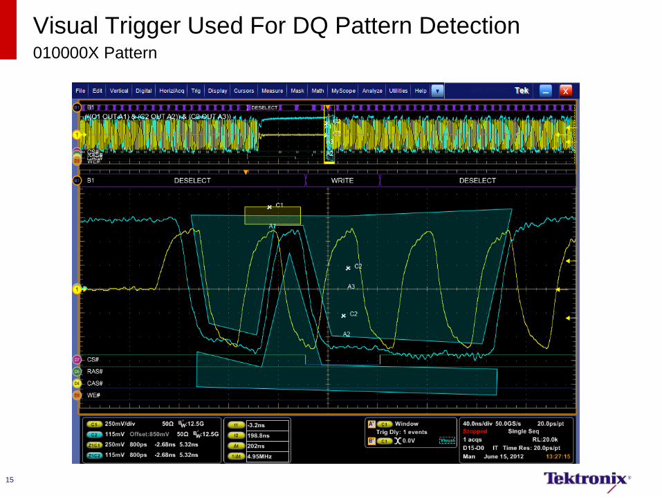
Visual Trigger Used For DQ Pattern Detection 010000X Pattern
15
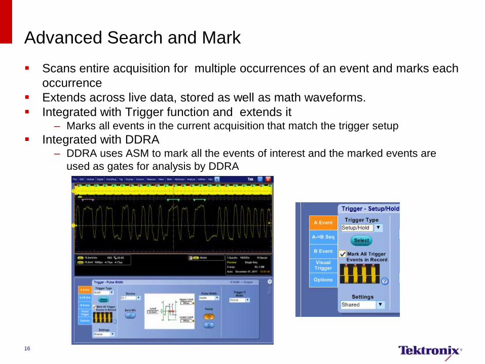
Advanced Search and Mark
Scans entire acquisition for multiple occurrences of an event and marks each
occurrence
Extends across live data, stored as well as math waveforms.
Integrated with Trigger function and extends it – Marks all events in the current acquisition that match the trigger setup
Integrated with DDRA – DDRA uses ASM to mark all the events of interest and the marked events are
used as gates for analysis by DDRA
16
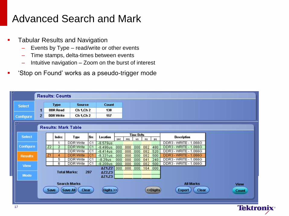
Advanced Search and Mark
Tabular Results and Navigation
– Events by Type – read/write or other events
– Time stamps, delta-times between events
– Intuitive navigation – Zoom on the burst of interest
‘Stop on Found’ works as a pseudo-trigger mode
17
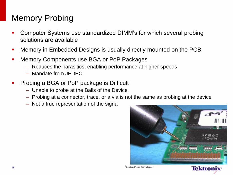
Memory Probing
Computer Systems use standardized DIMM’s for which several probing
solutions are available
Memory in Embedded Designs is usually directly mounted on the PCB.
Memory Components use BGA or PoP Packages
– Reduces the parasitics, enabling performance at higher speeds
– Mandate from JEDEC
Probing a BGA or PoP package is Difficult
– Unable to probe at the Balls of the Device
– Probing at a connector, trace, or a via is not the same as probing at the device
– Not a true representation of the signal
*Courtesy Micron Technologies 18
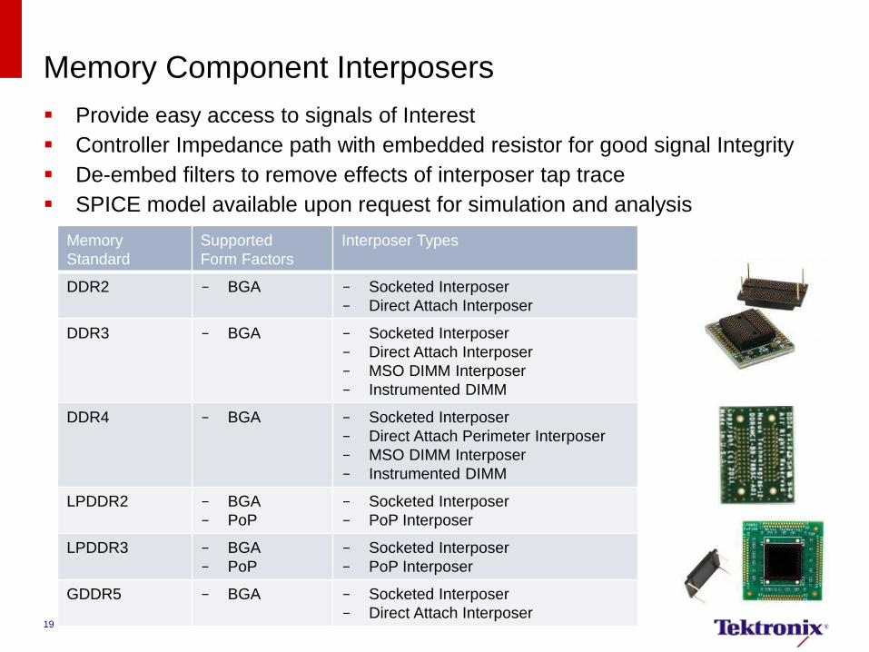
Memory Component Interposers
Memory
Standard
Supported
Form Factors
Interposer Types
DDR2 - BGA - Socketed Interposer
- Direct Attach Interposer
DDR3 - BGA
- Socketed Interposer
- Direct Attach Interposer
- MSO DIMM Interposer
- Instrumented DIMM
DDR4 - BGA - Socketed Interposer
- Direct Attach Perimeter Interposer
- MSO DIMM Interposer
- Instrumented DIMM
LPDDR2 - BGA
- PoP
- Socketed Interposer
- PoP Interposer
LPDDR3 - BGA
- PoP
- Socketed Interposer
- PoP Interposer
GDDR5 - BGA
- Socketed Interposer
- Direct Attach Interposer
Provide easy access to signals of Interest
Controller Impedance path with embedded resistor for good signal Integrity
De-embed filters to remove effects of interposer tap trace
SPICE model available upon request for simulation and analysis
19
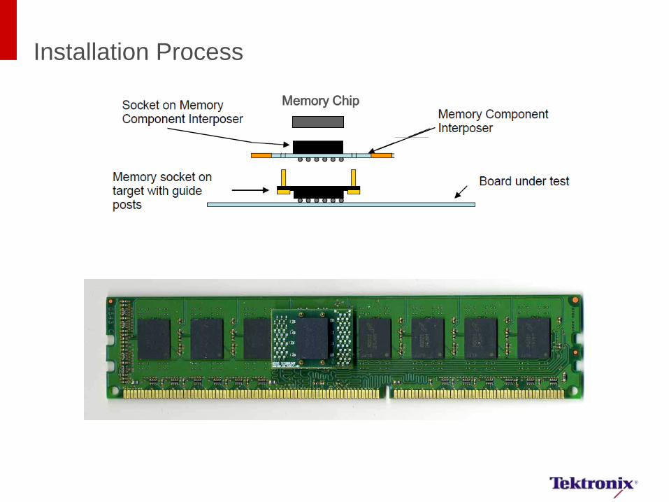
Installation Process
Memory Chip
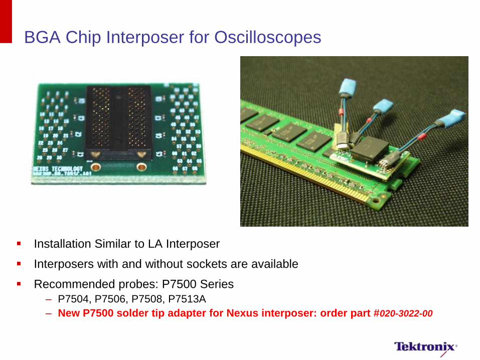
BGA Chip Interposer for Oscilloscopes
Installation Similar to LA Interposer
Interposers with and without sockets are available
Recommended probes: P7500 Series
– P7504, P7506, P7508, P7513A
– New P7500 solder tip adapter for Nexus interposer: order part #020-3022-00
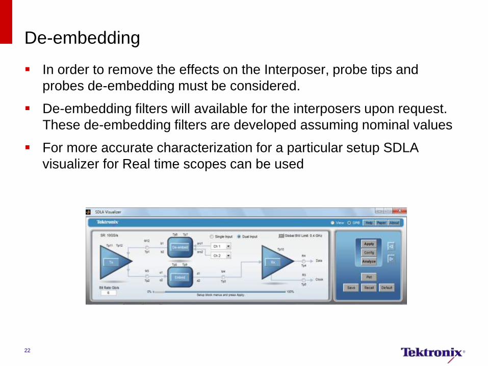
De-embedding
In order to remove the effects on the Interposer, probe tips and
probes de-embedding must be considered.
De-embedding filters will available for the interposers upon request.
These de-embedding filters are developed assuming nominal values
For more accurate characterization for a particular setup SDLA
visualizer for Real time scopes can be used
22
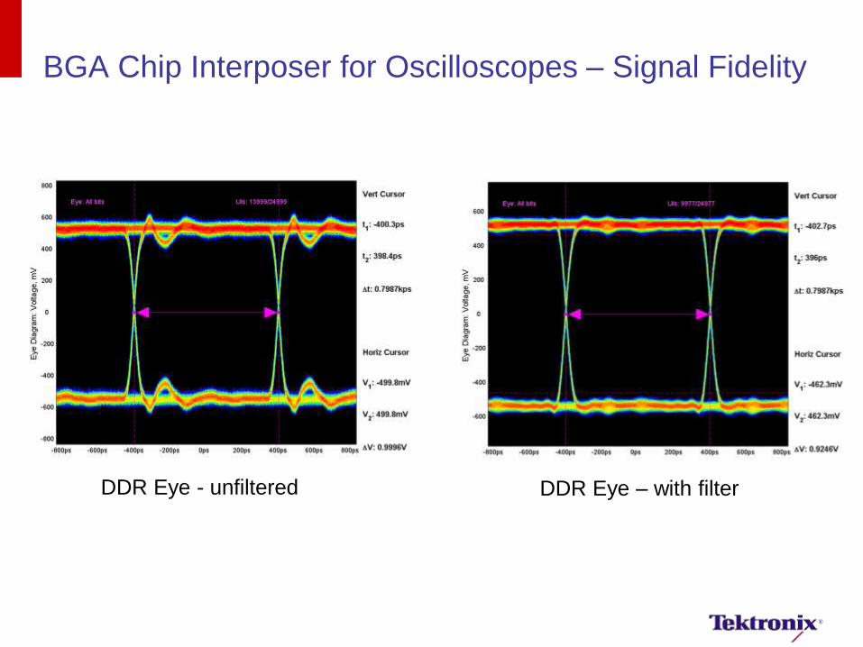
BGA Chip Interposer for Oscilloscopes – Signal Fidelity
DDR Eye – with filter
DDR Eye - unfiltered
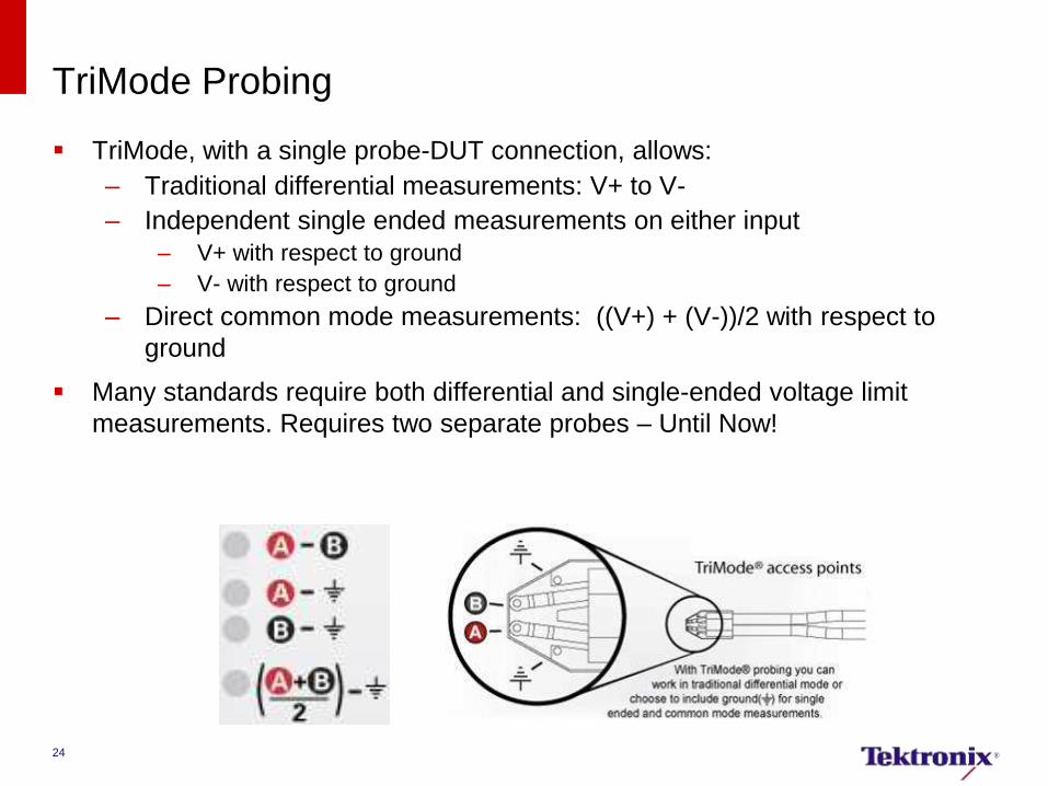
TriMode Probing
TriMode, with a single probe-DUT connection, allows:
– Traditional differential measurements: V+ to V-
– Independent single ended measurements on either input
– V+ with respect to ground
– V- with respect to ground
– Direct common mode measurements: ((V+) + (V-))/2 with respect to
ground
Many standards require both differential and single-ended voltage limit
measurements. Requires two separate probes – Until Now!
24
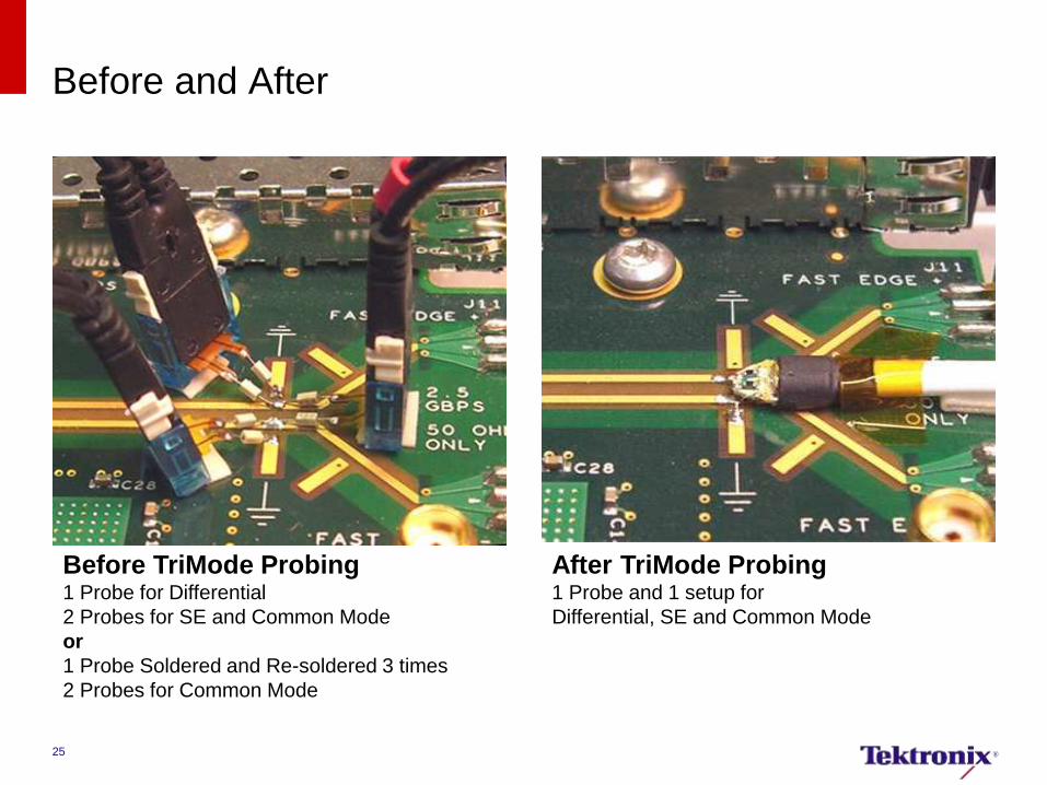
Before and After
Before TriMode Probing 1 Probe for Differential
2 Probes for SE and Common Mode
or
1 Probe Soldered and Re-soldered 3 times
2 Probes for Common Mode
After TriMode Probing 1 Probe and 1 setup for
Differential, SE and Common Mode
25
www.tektronix.com/ddr
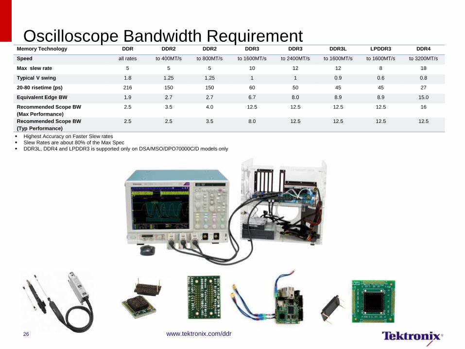
Memory Technology DDR DDR2 DDR2 DDR3 DDR3 DDR3L LPDDR3 DDR4
Speed all rates to 400MT/s to 800MT/s to 1600MT/s to 2400MT/s to 1600MT/s to 1600MT/s to 3200MT/s
Max slew rate 5 5 5 10 12 12 8 18
Typical V swing 1.8 1.25 1.25 1 1 0.9 0.6 0.8
20-80 risetime (ps) 216 150 150 60 50 45 45 27
Equivalent Edge BW 1.9 2.7 2.7 6.7 8.0 8.9 8.9 15.0
Recommended Scope BW
(Max Performance)
2.5 3.5 4.0 12.5 12.5 12.5 12.5 16
Recommended Scope BW
(Typ Performance)
2.5 2.5 3.5 8.0 12.5 12.5 12.5 12.5
Highest Accuracy on Faster Slew rates
Slew Rates are about 80% of the Max Spec
DDR3L, DDR4 and LPDDR3 is supported only on DSA/MSO/DPO70000C/D models only
Oscilloscope Bandwidth Requirement
26
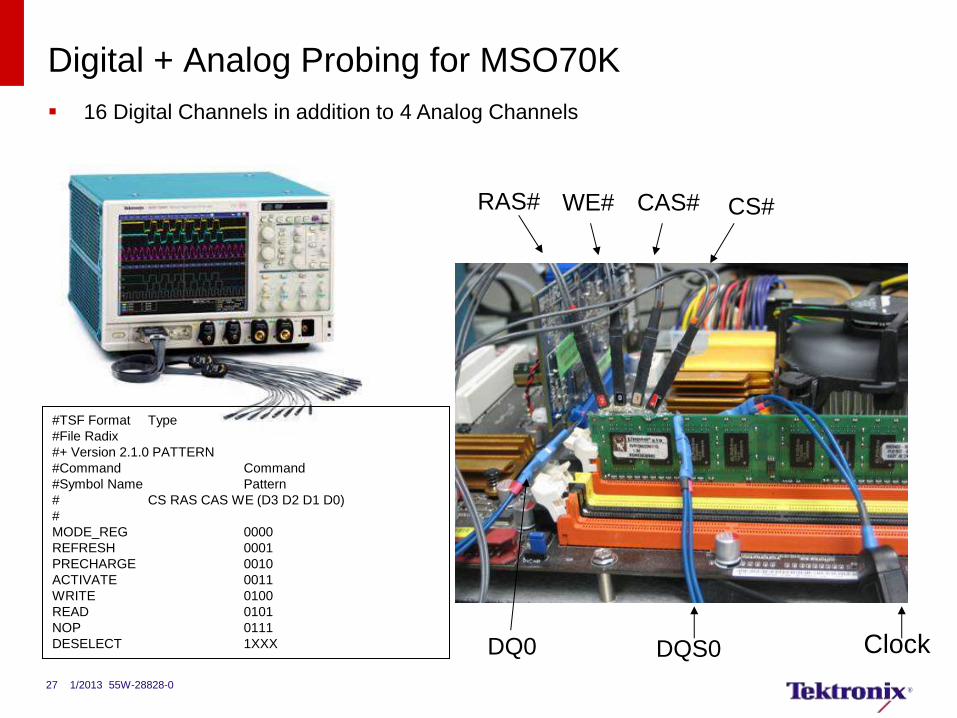
#TSF Format Type
#File Radix
#+ Version 2.1.0 PATTERN
#Command Command
#Symbol Name Pattern
# CS RAS CAS WE (D3 D2 D1 D0)
#
MODE_REG 0000
REFRESH 0001
PRECHARGE 0010
ACTIVATE 0011
WRITE 0100
READ 0101
NOP 0111
DESELECT 1XXX
Digital + Analog Probing for MSO70K
Clock DQS0 DQ0
RAS# WE# CAS# CS#
16 Digital Channels in addition to 4 Analog Channels
27 1/2013 55W-28828-0
2014/5/28 28
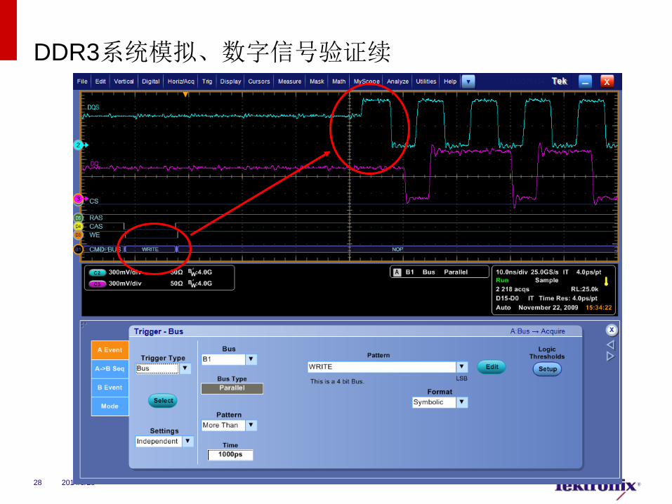
DDR3系统模拟、数字信号验证续
2014/5/28 29
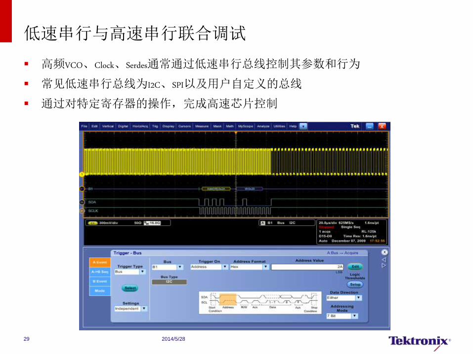
低速串行与高速串行联合调试
高频VCO、Clock、Serdes通常通过低速串行总线控制其参数和行为
常见低速串行总线为I2C、SPI以及用户自定义的总线
通过对特定寄存器的操作,完成高速芯片控制
2014/5/28 30
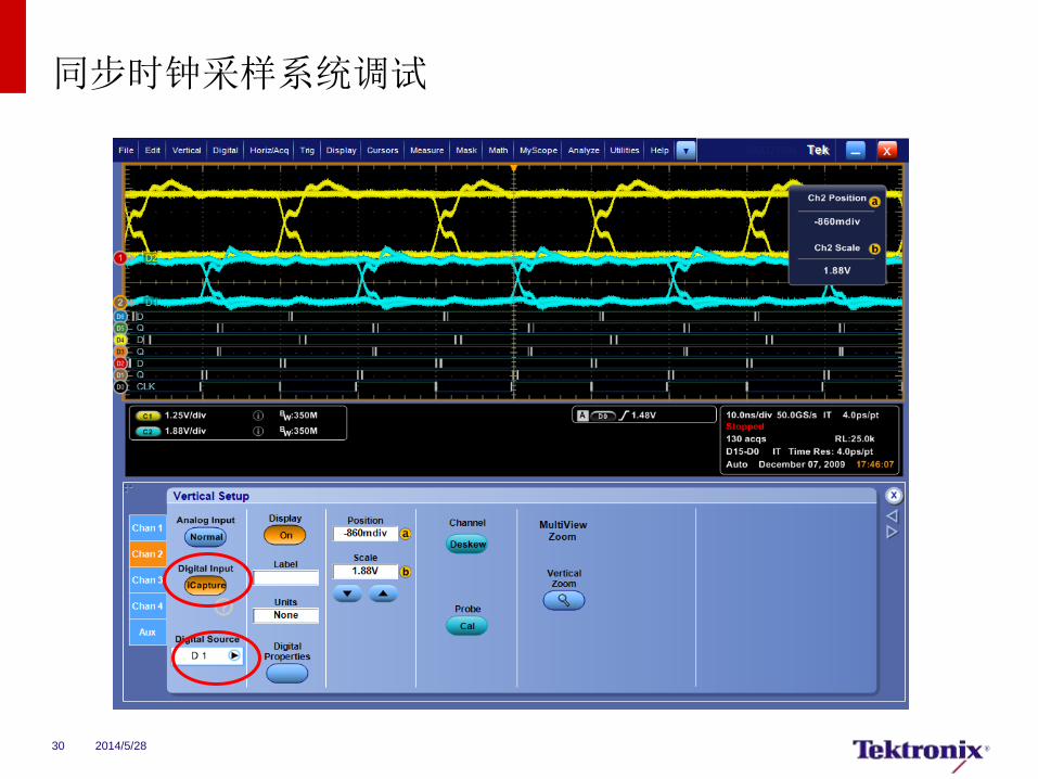
同步时钟采样系统调试
2014/5/28 31
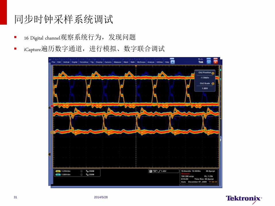
同步时钟采样系统调试
16 Digital channel观察系统行为,发现问题
iCapture遍历数字通道,进行模拟、数字联合调试
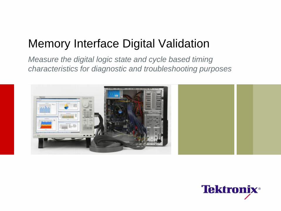
Memory Interface Digital Validation
Measure the digital logic state and cycle based timing
characteristics for diagnostic and troubleshooting purposes
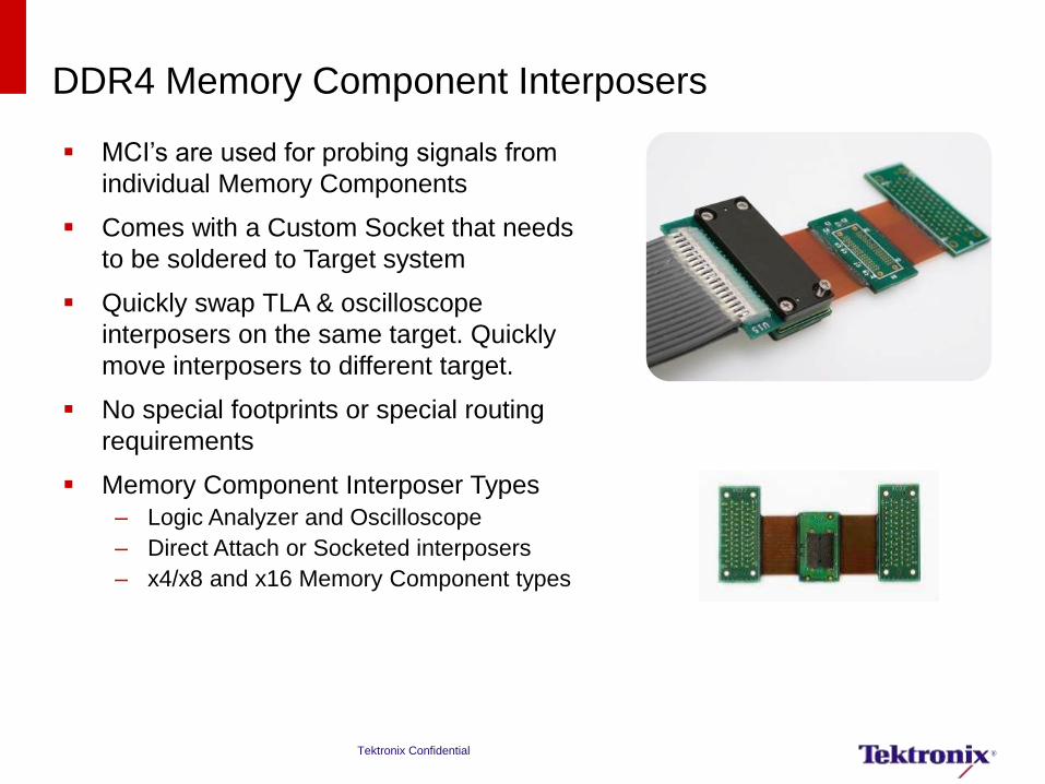
DDR4 Memory Component Interposers
Tektronix Confidential
MCI’s are used for probing signals from
individual Memory Components
Comes with a Custom Socket that needs
to be soldered to Target system
Quickly swap TLA & oscilloscope
interposers on the same target. Quickly
move interposers to different target.
No special footprints or special routing
requirements
Memory Component Interposer Types
– Logic Analyzer and Oscilloscope
– Direct Attach or Socketed interposers
– x4/x8 and x16 Memory Component types
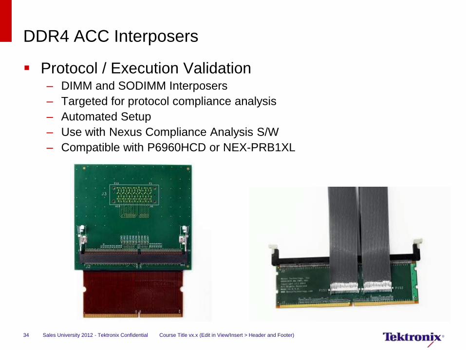
DDR4 ACC Interposers
Protocol / Execution Validation – DIMM and SODIMM Interposers
– Targeted for protocol compliance analysis
– Automated Setup
– Use with Nexus Compliance Analysis S/W
– Compatible with P6960HCD or NEX-PRB1XL
Sales University 2012 - Tektronix Confidential Course Title vx.x (Edit in View/Insert > Header and Footer) 34
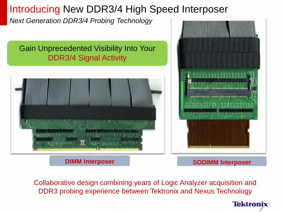
DIMM Interposer SODIMM Interposer
Gain Unprecedented Visibility Into Your
DDR3/4 Signal Activity
Introducing New DDR3/4 High Speed Interposer Next Generation DDR3/4 Probing Technology
Collaborative design combining years of Logic Analyzer acquisition and
DDR3 probing experience between Tektronix and Nexus Technology
New DDR3/4 High Speed Interposer Next Generation DDR3/4 Probing Technology
Provides significant performance improvements to DDR3 probing
– Integrates Tektronix ultra-high performance SiGe Hybrid ASIC
technology
– Compensation for platform trace loss on writes
Improved interposer input impedance (5.2k to 0.73V)
– Reduces load on target with minimal effect on bus
– Provides an accurate representation of the signal on the target
Enables probing DDR3/4 speeds at 2400MT/s and beyond
Enables probing lower voltage signals on LVDDR3/4
Interposers compatible with UDIMM, RDIMM, LRDIMM
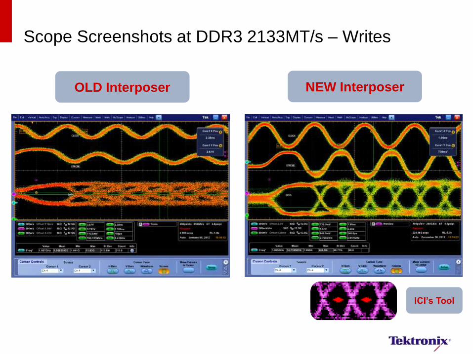
Scope Screenshots at DDR3 2133MT/s – Writes
OLD Interposer NEW Interposer
ICI’s Tool
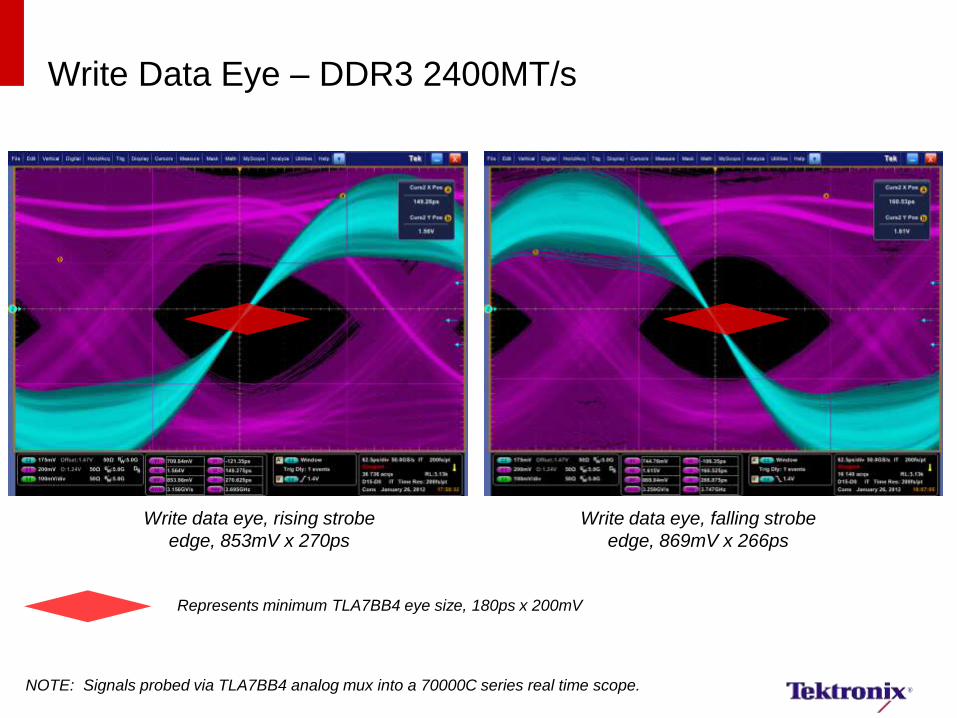
Write Data Eye – DDR3 2400MT/s
Write data eye, rising strobe
edge, 853mV x 270ps
Write data eye, falling strobe
edge, 869mV x 266ps
NOTE: Signals probed via TLA7BB4 analog mux into a 70000C series real time scope.
Represents minimum TLA7BB4 eye size, 180ps x 200mV
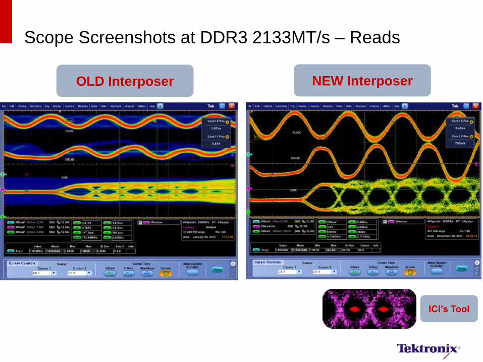
Scope Screenshots at DDR3 2133MT/s – Reads
OLD Interposer NEW Interposer
ICI’s Tool
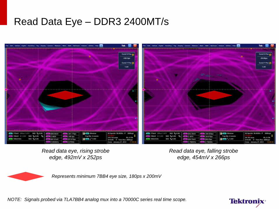
Read Data Eye – DDR3 2400MT/s
Read data eye, rising strobe
edge, 492mV x 252ps
Read data eye, falling strobe
edge, 454mV x 266ps
NOTE: Signals probed via TLA7BB4 analog mux into a 70000C series real time scope.
Represents minimum 7BB4 eye size, 180ps x 200mV

TLA7BBx Logic Analyzer Modules Proven Technology for Analyzing DDR3 SDRAM
50GS/s (20ps)
Memory Depth
TLA7BB3 TLA7BB4 TLA7BB2 DIGITAL CHARACTERISTICS
Digital Channels
High Speed Timing (MagniVu)
Deep Memory Timing
State Speed
68 102 136
Up to 6.4GS/s
Up to 1.4GHz/3.0Gbps
Standard 2Mb, Maximum 64Mb
Probes All P68xx and P69xx
iCapture (Analog Mux) 3 GHz
Preserve investment in TLA7BBx modules
Enable higher DDR3 speed support with new interposer
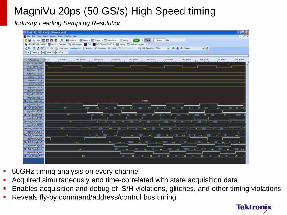
MagniVu 20ps (50 GS/s) High Speed timing Industry Leading Sampling Resolution
50GHz timing analysis on every channel
Acquired simultaneously and time-correlated with state acquisition data
Enables acquisition and debug of S/H violations, glitches, and other timing violations
Reveals fly-by command/address/control bus timing
43
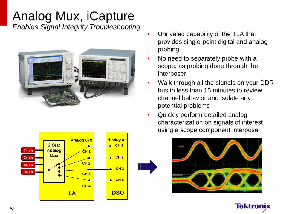
Analog Mux, iCapture Enables Signal Integrity Troubleshooting
Unrivaled capability of the TLA that
provides single-point digital and analog
probing
No need to separately probe with a
scope, as probing done through the
interposer
Walk through all the signals on your DDR
bus in less than 15 minutes to review
channel behavior and isolate any
potential problems
Quickly perform detailed analog
characterization on signals of interest
using a scope component interposer Trigger State
Machine
4 ch
CH 1
CH 2
CH 3
CH 4
DSO LA
Analog In
CH 1
CH 2
CH 3
CH 4
Analog Out
3 GHz
Analog
Mux
34 ch
34 ch
34 ch
34 ch
44
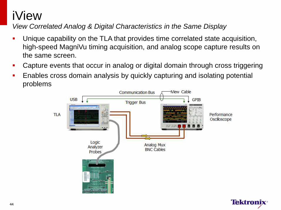
iView View Correlated Analog & Digital Characteristics in the Same Display
Unique capability on the TLA that provides time correlated state acquisition,
high-speed MagniVu timing acquisition, and analog scope capture results on
the same screen.
Capture events that occur in analog or digital domain through cross triggering
Enables cross domain analysis by quickly capturing and isolating potential
problems
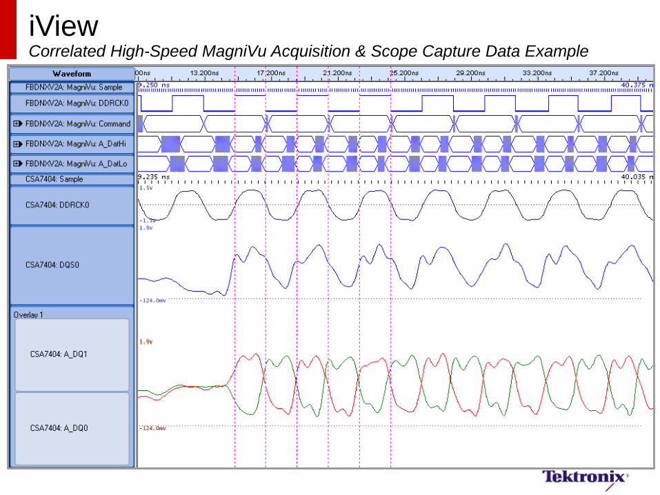
iView Correlated High-Speed MagniVu Acquisition & Scope Capture Data Example
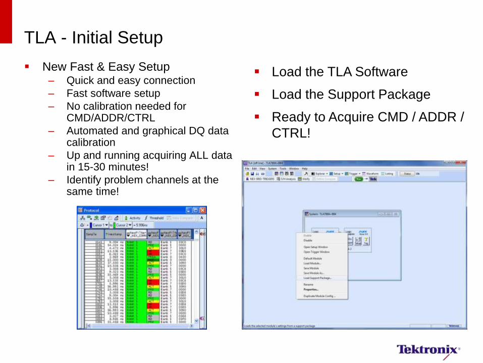
Load the TLA Software
Load the Support Package
Ready to Acquire CMD / ADDR /
CTRL!
TLA - Initial Setup
New Fast & Easy Setup – Quick and easy connection
– Fast software setup
– No calibration needed for CMD/ADDR/CTRL
– Automated and graphical DQ data calibration
– Up and running acquiring ALL data in 15-30 minutes!
– Identify problem channels at the same time!
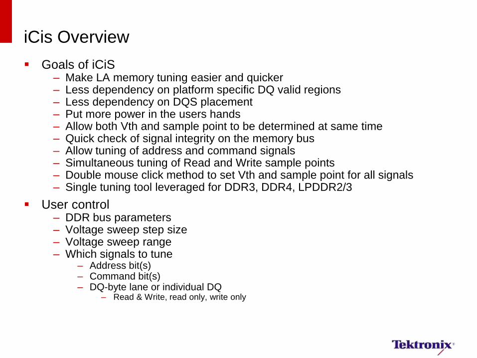
iCis Overview
Goals of iCiS – Make LA memory tuning easier and quicker – Less dependency on platform specific DQ valid regions – Less dependency on DQS placement – Put more power in the users hands – Allow both Vth and sample point to be determined at same time – Quick check of signal integrity on the memory bus – Allow tuning of address and command signals – Simultaneous tuning of Read and Write sample points – Double mouse click method to set Vth and sample point for all signals – Single tuning tool leveraged for DDR3, DDR4, LPDDR2/3
User control – DDR bus parameters – Voltage sweep step size – Voltage sweep range – Which signals to tune
– Address bit(s) – Command bit(s) – DQ-byte lane or individual DQ
– Read & Write, read only, write only
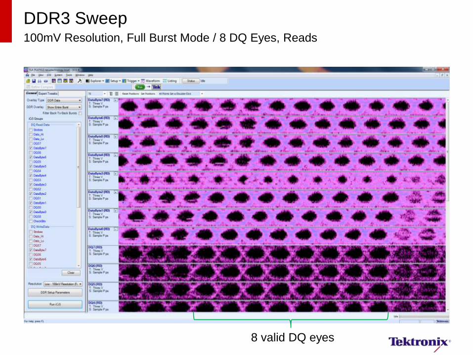
DDR3 Sweep 100mV Resolution, Full Burst Mode / 8 DQ Eyes, Reads
8 valid DQ eyes
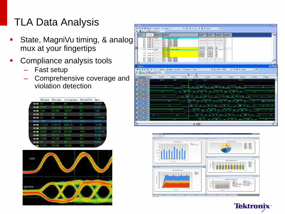
TLA Data Analysis
State, MagniVu timing, & analog mux at your fingertips
Compliance analysis tools – Fast setup
– Comprehensive coverage and violation detection
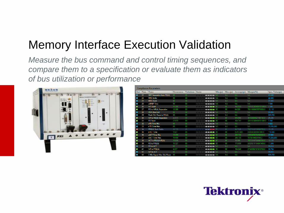
Memory Interface Execution Validation Measure the bus command and control timing sequences, and
compare them to a specification or evaluate them as indicators
of bus utilization or performance
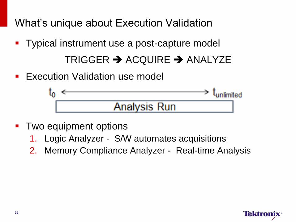
What’s unique about Execution Validation
Typical instrument use a post-capture model
TRIGGER ACQUIRE ANALYZE
Execution Validation use model
Two equipment options
1. Logic Analyzer - S/W automates acquisitions
2. Memory Compliance Analyzer - Real-time Analysis
52
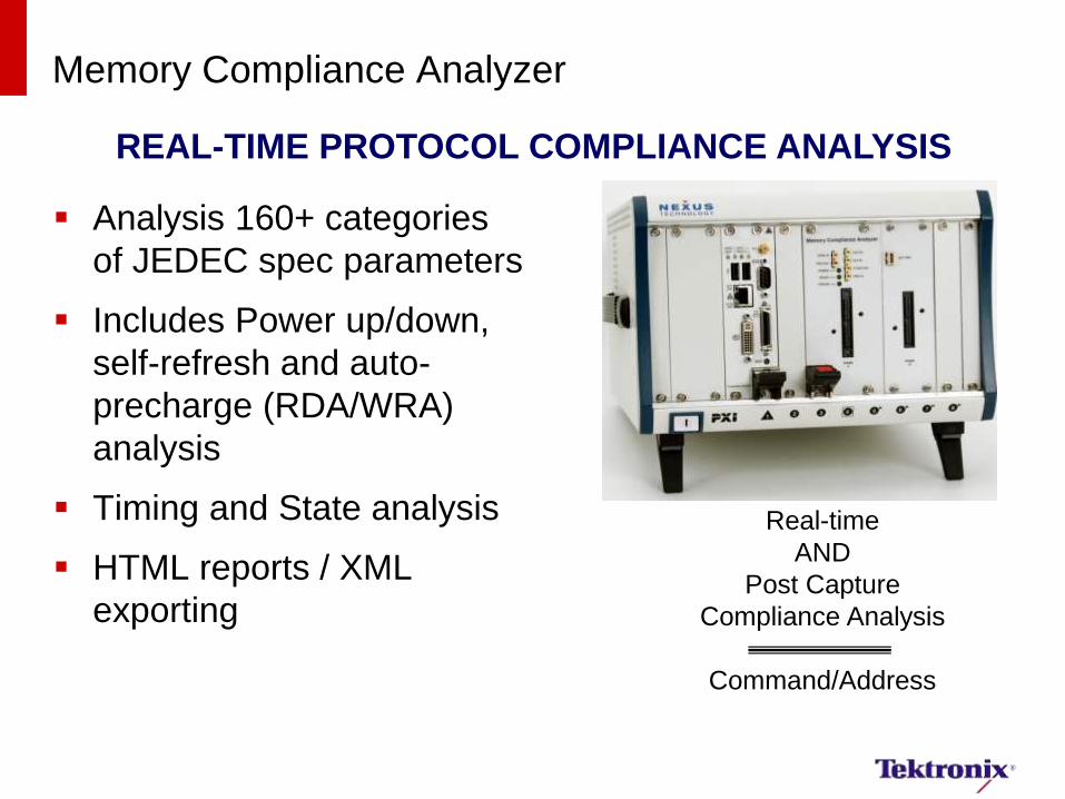
Memory Compliance Analyzer
REAL-TIME PROTOCOL COMPLIANCE ANALYSIS
Real-time
AND
Post Capture
Compliance Analysis
Command/Address
Analysis 160+ categories
of JEDEC spec parameters
Includes Power up/down,
self-refresh and auto-
precharge (RDA/WRA)
analysis
Timing and State analysis
HTML reports / XML
exporting
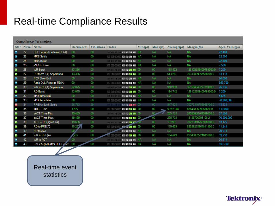
Real-time Compliance Results
Real-time event
statistics
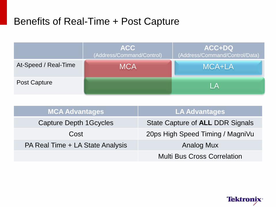
Benefits of Real-Time + Post Capture
MCA Advantages LA Advantages
Capture Depth 1Gcycles State Capture of ALL DDR Signals
Cost 20ps High Speed Timing / MagniVu
PA Real Time + LA State Analysis Analog Mux
Multi Bus Cross Correlation
ACC (Address/Command/Control)
ACC+DQ (Address/Command/Control/Data)
At-Speed / Real-Time
Post Capture
MCA
LA
MCA+LA

Memory Validation Continuum
Analysis SW
Analog
Validation
Instruments
Probes
71
Digital
Validation
Execution
Validation