Embed Size (px)
Citation preview


Business Areas
Graphene Square, Inc. is a pioneer in the commercialization of graphene material and graphene films for use as a
transparent conductor and in other electronics applications. Established in 2012 as a spin-off of the research of Prof.
Byung Hee Hong at Seoul National University and with headquarters in Seoul, Korea.
Our mission is to be the world’s first company commercializing CVD graphene technology and No.1 cost-competitive
& best-quality graphene film supplier in both rigid and flexible electronic markets.
CVD Synthesis Systems
For researchers who want to synthesize their
own graphene or 2D materials, Graphene
Square markets a low-cost thermal CVD
system that allows the users to easily begin
synthesizing their own large-area, high-
quality graphene and 2D materials samples
in a lab environment. Graphene Square also
provides training programs covering the
current best practices for graphene growth,
etching, patterning, and transfer. Other
custom CVD systems are available for the
synthesis of various 2D materials such as
MoS2, WSe2, h-BN, etc.
Graphene Samples & Fab. Services
Using state-of-the-art chemical vapor
deposition (CVD) methods developed in-
house, Graphene Square offers the highest
quality graphene samples currently on the
market. In addition to the standard samples
available online, Graphene Square can
provide various fab. services including the
sample transfer on the customers’ own
substrates as well as end-equipment
prototype devices. Graphene Square also
supplies graphene oxides (GOs) and
graphene quantum dots (GQDs) for various
biological, display, and energy researches.
IP Licensing & Consultant
Graphene Square provides general
consulting services and also licenses
technology from its extensive patent
portfolio, which has been recently
highlighted by Bloomberg and Businessweek.
Areas covered include: industrial graphene
synthesis, transfer, and patterning using roll-
to-roll techniques and their applications to
current consumer electronic products as well
as future applications including flexible and
wearable electronics.
GSI’s Patent Portfolio
Large ScaleGraphene Synthesis
73 PatentsCVD Graphene
Graphene OxidesGraphene QDs
Nano InkMaterials
HeatDissipation
UltralightMaterials
EnergyElectrodes
NextGeneration
Devices
TransparentElectrodes
Nano InkMaterials
BarrierMaterials
3 Patent Flexible Displays Touch Sensors
2 Patent Display Solar CellAnti-OxidationHeat Insulation
2 Patent LEDs, BLUsECUs &PC Electronic
2 Patent Automobile &Aerospace Applications
15 Patent Flexible Displays Touch Sensors
3 Patent Ultrahigh Speed Transistors/Photosensors RFID
13 Patent Solar CellsSecondary BatteryFuel CellsSuper Capacitors

CVD Systemsfor Graphene &2D MaterialsSophisticated · Cost Effective · Reliable · Programmable Systems · for Highest Sample Quality Fast Heating & Cooling · World’s Best Training Service Available
The development of Graphene Square’s CVD systems is based on the researches of Prof.
Byung Hee Hong who reported the synthesis of large-area graphene by CVD for the first time
in 2009. His continuous efforts toward the industrial synthesis of high-quality graphene
enabled the development of most-reliable and cost-effective synthesis systems not only for
graphene but also for h-BN and other 2D materials. The performance of our CVD systems for
R&D have been proven by more than 100 systems installed across the world. Graphene Square
also provides the world’s best training service to researchers, including the latest synthesis,
transfer, and patterning processes needed for the fabrication of the best-quality devices.
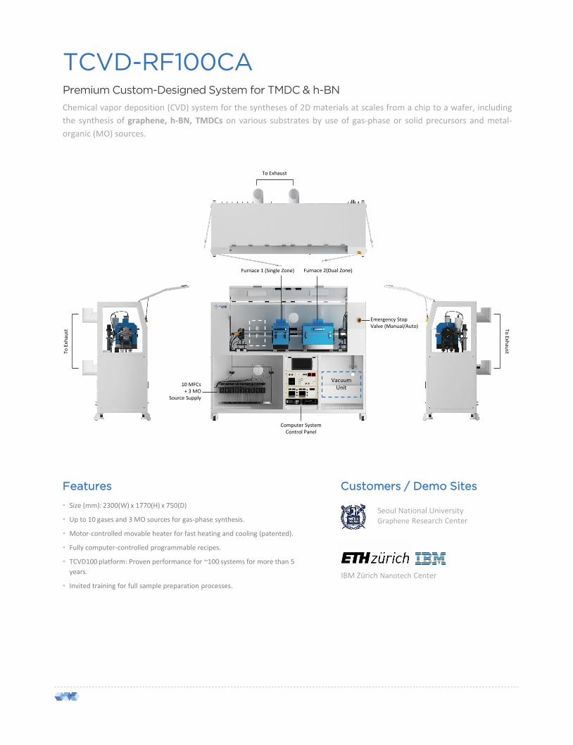
Features
• Size (mm): 2300(W) x 1770(H) x 750(D)
• Up to 10 gases and 3 MO sources for gas-phase synthesis.
• Motor-controlled movable heater for fast heating and cooling (patented).
• Fully computer-controlled programmable recipes.
• TCVD100 platform: Proven performance for ~100 systems for more than 5
years.
• Invited training for full sample preparation processes.
Customers / Demo Sites
TCVD-RF100CAPremium Custom-Designed System for TMDC & h-BN
Chemical vapor deposition (CVD) system for the syntheses of 2D materials at scales from a chip to a wafer, including
the synthesis of graphene, h-BN, TMDCs on various substrates by use of gas-phase or solid precursors and metal-
organic (MO) sources.
To Exhaust
To Exh
aust To
Exh
aust
Vacuum Unit
Emergency Stop Valve (Manual/Auto)
Furnace 1 (Single Zone)
RF
Computer System Control Panel
Furnace 2(Dual Zone)
10 MFCs + 3 MO
Source Supply
IBM Zürich Nanotech Center
Seoul National UniversityGraphene Research Center

GRAPHENE SQUARE PRODUCT BROCHURE
Technical Specification
02….03
CVD Reactor • Tube type 4 inch diameter quartz
Substrate Size• Lateral insertion of 10 mm to < 4 inch wafers possible. (Loading frames for small samples)
• Rolled metallic foils can be loaded to synthesize A4 sized or larger 2D materials.
Heating
• Dual-zone heater and controller for graphene/h-BN synthesis. Single-zone precursor heater and Dual-
zone deposition heater for TMDC synthesis.
• The heaters are movable along two rails and the distance can be motor-controlled, enabling 10ºC/sec
or faster temperature change rate.
Base Pressure • 10-5 mbar (depending on the dryness of source)
Operating Pressure • 10-3 mbar – 1 bar
Precursor• Max 10 gas lines (ex. CH4, C2H4, NH3, B2H6, Ar, H2, H2S, H2Se, N2, O2) + 2 extra ports.
• Metal oxide sources of various transition metals placed in Heat Zone 1 for solid source growth.
Other metal organic (MO) sources
• Extra 3 Metal-Organic Source Injection Ports are included. (ex Mo(CO)6, Fe(CO)5)
• Low-T cold trap for residual sources.
Flow control
• Precursor gases: 0.1 – 10 sccm
• Other gases: 10 – 1000 sccm
• Automatic flow control.
Vacuum
• Turbo pump 450 l/s (ISO160) < 10-6 mbar.
• Dry scroll pump < 10-1 mbar.
• Main Gate Valve Pneumatic type / Fore-line / roughing Angle Valve / Foamed bellows
• By-pass pumping adaptor, clamp & centering.
T-measurement • Standard Thermocouple (NIR calibrated)
Sample switching • Position switching by sample loading stage.
System Control
• Control PC system (12" touch, dual core)
• Serial Network module (4-ch)
• Remote IO module (RS485)
• System base programming / System recipe control module / System date file save module
• Software upgrade support.
• Gas valve, angle valve Open/Close / Rotary pump On/Off switch / Main power On/Off switch
• Cooling water & air pressure switch.

Features
• Size(mm): 3000(W) x 1800(H) x 750(D)
• Up to 10 gases and 3 MO sources for gas-phase synthesis.
• Motor-controlled movable heater for fast heating and cooling (patented).
• Fully computer-controlled programmable recipes.
• TCVD100 platform: Proven performance for ~100 systems for more than 5
years.
• Invited training for full sample preparation processes from synthesis,
etching, and transfer.
• Supply of high-quality source materials.
• 1 year warranty included (2 year extended warranty available)
• CVD chambers connected to a Glove Box. Free from air exposure.
Customers / Demo Sites
TCVD-DC100CA
Chemical vapor deposition (CVD) system for the syntheses of 2D materials at scales from a chip to a wafer, including
the synthesis of graphene, h-BN, TMDCs on various substrates by use of gas-phase or solid precursors and metal-
organic (MO) sources. The synthesized samples can be transferred to a glove box filled with inert gases for further
processes without exposure to air environment.
University of North Texas
Seoul National UniversityGraphene Research Center
Premium Custom Design Dual CVD System with a Glove Box

GRAPHENE SQUARE PRODUCT BROCHURE
Technical Specification
04….05
CVD Reactor
• Dual Tube type 4 inch diameter quartz.
• Remote Microwave Plasma Module.
• Connected to a Glove Box.
Substrate Size• Lateral insertion of 10 mm to <4 inch wafers possible. (Loading frames for small samples )
• Rolled metallic foils can be loaded to synthesize A4 sized or larger 2D materials.
Heating
• Dual-zone heater and controller for graphene/h-BN synthesis. Single-zone precursor heater and Dual-
zone deposition heater for TMDC synthesis.
• The heaters are movable along two rails and the distance can be motor-controlled, enabling 10ºC/sec
or faster temperature change rate.
Base Pressure • 10-5 mbar (depending on the dryness of source)
Operating Pressure • 10-3 mbar – 1 bar
Precursor• Max 10 gas lines (ex. CH4, C2H4, NH3, B2H6, Ar, H2, H2S, H2Se, N2, O2) + 2 extra ports.
• Metal oxide sources of various transition metals placed in Heat Zone 1 for solid source growth.
Other metal organic (MO) sources
• Extra 3 Metal-Organic Source Injection Ports are included. (ex Mo(CO)6, Fe(CO)5)
• Low-T cold trap for residual sources.
Flow control
• Precursor gases: 0.1 – 10 sccm
• Other gases: 10 – 1000 sccm
• Automatic flow control.
Vacuum
• Turbo pump 450l/s (ISO160) < 10-6 mbar.
• Dry scroll pump < 10-1 mbar.
• Main Gate Valve Pneumatic type / Fore-line / roughing Angle Valve / Foamed bellows
• By-pass pumping adaptor, clamp & centering.
T-measurement • Standard Thermocouple (NIR calibrated)
Sample switching • Position switching by sample loading stage.
System Control
• Control PC system (12" touch, dual core)
• Serial Network module (4-ch)
• Remote IO module (RS485)
• System base programming / System recipe control module / System date file save module
• Software upgrade support.
• Gas valve, angle valve Open/Close / Rotary pump On/Off switch / Main power On/Off switch
• Cooling water & air pressure switch.
TCVD-50B
Features
• Size(mm): 1500(W) x 893(H) x 590(D)
• Economic & space-saving model.
• Optimized for graphene, CNT, h-BN and TMDC growth.
• Water-cooled end chambers and doors.
• Process Temperature: ~1,100
• Protective design from heat
• Uniformity of Film Thickness: ≤+-3%
• Testing Uniformity: ≤+-3%
• Movable furnace method is our unique knowhow for fast heating and fast
cooling of the sample
Customization
Furnace
• Single – 2 Heating Zones (Standard)
• Dual – 3 Heating Zones
• Single + RF M/W Module
Chamber Size
• 2 inch (Standard)
• 4 inch
Pumping Unit
• Oil Type Rotary Pump (Standard)
• Dry Scroll Pump
• Additional: Mechanical Turbo Pump
Gas Control Unit
• 3 MFCs +1 Spare (Standard)
• Up to 5 MFCs
Warranty
• 1 year – Included (Standard)
• 2 years – Optional
This small-size equipment has been developed on customers’ demand for the lower cost but higher quality synthesis
of graphene and 2D materials. TCVD-50B is the most ideal system for researchers who are limited in budget. The
versatile specifications from fully manual to semi-automatic systems can be adjusted to fit the customers’ budget. We
recommend this system for training or laboratory classes, and the detailed instructing program and materials will be
provided upon purchase.
2-Inch Table-Top Manual Type Thermal CVD

Price will be determined after consultation. (Different customization from the
standard parts will affect the overall price.)*
GRAPHENE SQUARE PRODUCT BROCHURE
TCVD-100A
Features
• Size(mm): 1750(W) x 1585(H) x 750(D)
• Advanced Semi-Auto System
• Optimized for graphene, CNT, h-BN and TMDC growth
• Water-cooled end chambers and doors
• Process Temperature: ~1,100
• Uniformity of Film Thickness: ≤+-3%
• Testing Uniformity: ≤+-3%
• Movable furnace method is our unique knowhow for fast heating and fast
cooling of the sample
• Standard safety box
Customization
Furnace
• Single – 2 Heating Zones (Standard)
• Dual – 3 Heating Zones
• Single + RF M/W Module
Chamber Size
• 2 inch
• 4 inch (Standard)
• 6 inch
• 8 inch
Pumping Unit
• Oil Type Rotary Pump (Standard)
• Dry Scroll Pump
• Additional: Mechanical Turbo Pump
Gas Control Unit
• 3 MFCs +1 Spare (Standard)
• Up to 8 MFCs
Warranty
• 1 year – Included (Standard)
• 2 years – Optional
06….07
Proven performance in more than 100 systems installed in Korea.World-wide customers in US, EU, Middle East, and Asia countries.
Customers
TCVD-100A is a very sophisticated and cost effective CVD system that can be equipped with semi-automatic or fully
programmable gas-flow and temperature control modules. It is the most ideal equipment for the synthesis of high
quality graphene and h-BNs, which can be easily extended to various 2D materials synthesis. The safety cabinet that
covers the whole system protects users from any hazardous event, and the emergency stop button will ensure the
safety even further.
Standard 4-Inch Thermal CVD System with a Safety Cabinet

TCVD-D100CA
Features
• Size(mm): 2300(W) x 1770(H) x 750(D)
• Advanced Computer Controlled Automatic System
• Optimized for graphene, CNT, h-BN and TMDC growth
• Water-cooled end chambers and doors
• Process Temperature: ~1,100
• Uniformity of Film Thickness: ≤+-3%
• Testing Uniformity: ≤+-3%
• Movable furnace method is our unique knowhow for fast heating and fast
cooling of the sample.
• Standard safety box
Customization
Furnace
• Single – 2 Heating Zones
• Dual – 3 Heating Zones (Standard)
• Triple – 4 Heating Zones
• Single or Dual + RF M/W Module
Chamber Size
• 2 inch
• 4 inch (Standard)
• 6 inch
• 8 inch
Pumping Unit
• Oil Type Rotary Pump (Standard)
• Dry Scroll Pump
• Additional: Mechanical Turbo Pump
Gas Control Unit
• 3 MFCs +1 Spare (Standard)
• Up to 10 MFCs
Warranty
• 1 year – Included (Standard)
• 2 years – Optional
Customers
Price will be determined after consultation. (Different customization from the
standard parts will affect the overall price.)*
TCVD-D100CA is an advanced equipment dedicated to the growth of TMDC materials such as MoS2, WSe2, etc. The
computer-aided controlling module promises the reliable growth condition for multiple users. The movable dual
furnace system enables the fast heating and fast cooling of source materials and substrates, which is important for the
synthesis of higher quality TMDCs. The safety housing with emergency alarm/stop functions will ensure the safe
operation by users.
4-Inch Automatic Dual-Furnace CVD System for TMDC Synthesis

The Highest Quality CVD Graphene Films on Custom Substrates · Graphene Oxides (GOs)Graphene Quantum Dots (GQDs) · Consumables for Graphene Researches
Using state-of-the-art chemical vapor deposition (CVD) methods developed in-house,
Graphene Square offers the highest quality graphene samples currently on the market.
In addition to the standard samples available online, Graphene Square can provide
various fab. services including the sample transfer on the customers’ own substrates as
well as end-equipment prototype devices. Graphene Square also supplies graphene
oxides (GOs) and graphene quantum dots (GQDs) applicable to various biological,
display, and energy researches.
Graphene Samples

GRAPHENE SQUARE PRODUCT BROCHURE
Sungkyunkwan Univ. (SKKU) famous for the world’s most graphene patent applications has transferred the most
important graphene-related 42 patents to Graphene Square Inc. in 2012.
BBC News “Graphene : patent surge reveals global race
IP Development & Licensing
20 21 32 1
Registered Patents Applied Patents
(Domestic)
Applied Patents
(International)
Registered Design
(GSI Logo)
134
Sungkyunkwan
Univ. (Korea)
97
Zhejiang Univ.
(China)
92
Tsinghua Univ.
(China)
56
Rice Univ.
(US)
34
MIT (US)
16
Manchester
Univ.
Graphene Square’s IPs (June 20, 2014)
GSI‘s Key Patents Highlighted by Bloomberg & Businessweek
“Hong’s patents are key in making cost-efficient, large-scale graphene
for touchscreen panels in mass volume.”
(Samsung-Apple Smartphone Battleground Is Single Atom Thick May 15,
2014, Bloomberg.com)
10….11

CVD Graphene on Cu foils
2 nm2 nm
High-Resolution TEM Images Raman Spectrum (after transfer)
(1) S. Bae*, H. Kim* et al. Roll-to-roll production of 30 inch graphene
films for transparent electrodes Nature Nanotech. 5, 574 (2010).
(2) Y. Lee et al. Wafer-Scale Synthesis and Transfer of Graphene
Films.Nano Lett. 10, 490-493 (2010).
(3) H.-A-S. Shin et al. Graphene-induced Unusual Microstructural
Evolution in Ag Plated Cu Foils. Nanoscale 6, 7209-7214 (2014).
(4) Hae-A-Seul Shin*, Jaychul Ryu* et al. Highly Uniform Growth of
Monolayer Graphene by Chemical Vapor Deposition on Cu-Ag Alloy
Catalysts. Phys. Chem. Chem. Phys. 16, 3087-3094 (2014).
ReferenceSEM Image of Graphene on Cu
Product Size Up to 500x600
Film Morphology Continuous Monolayer (>95%)
Sheet Resistance -
Mobility >3500cm2/Vs
Transmittance >97%
Substrate Cu foil (35 thick)
Domain Size 10-20
GRAPHENE SQUARE PRODUCT BROCHURE
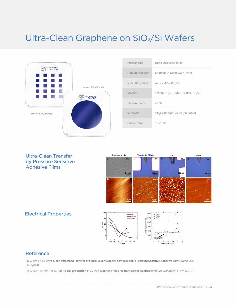
Ultra-Clean Graphene on SiO2/Si Wafers
Electrical Properties
Ultra-Clean Transfer
by Pressure Sensitive
Adhesive Films
(1) S. Kim et. al. Ultra-Clean Patterned Transfer of Single-Layer Graphene by Recyclable Pressure Sensitive Adhesive Films. Nano Lett.
(accepted).
(2) S. Bae*, H. Kim* et al. Roll-to-roll production of 30 inch graphene films for transparent electrodes Nature Nanotech. 5, 574 (2010).
Reference
4-inch SiO2/Si wafer
Product Size Up to 90 x 90 (Max)
Film Morphology Continuous Monolayer (>95%)
Sheet Resistance Av. < 250~400 Ω/sq
Mobility >3500 cm2/Vs (Max. 17,000 cm2/Vs)
Transmittance >97%
Substrate SiO2(300nm)/Si wafer (Standard)
Domain Size 10-20
12….13
1x1 cm2 SiO2/Si chips

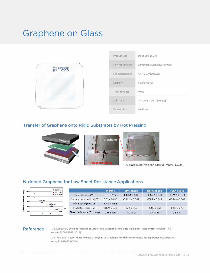
Sheet Resistance Uniformity
Graphene on PET
Ohm/Sq.
Product Size Up to 500 x 600
Film Morphology Continuous Monolayer (>95%)
Sheet Resistance Av. < 250~400 Ω/sq
Mobility >3500 cm2/Vs
Transmittance >97%
Substrate PET (188) (Standard)
Domain Size 10-20
Application of Graphene on PET for
Flexible Touch Screen
J.-H. Ahn & B. H. Hong Graphene for displays that bend. Nature Nanotech. 9, 737-738 (2014).Reference
Mechanical Properties of Graphene on PET Optical Transmittance
GRAPHENE SQUARE PRODUCT BROCHURE
Graphene on Glass
graphene
Precise matchingA glass substrate for passive matrix LCDs
(1) J. Kang et al. Efficient Transfer of Large-Area Graphene Films onto Rigid Substrates by Hot Pressing. ACS
Nano 6, 53060-5365 (2012)
(2) Y. Kim et al. Vapor-Phase Molecular Doping of Graphene for High-Performance Transparent Electrodes. ACS
Nano, 8 , 868–874 (2014).
Reference
Transfer of Graphene onto Rigid Substrates by Hot Pressing
N-doped Graphene for Low Sheet Resistance Applications
Product Size Up to 80 x 150
Film Morphology Continuous Monolayer (>95%)
Sheet Resistance Av. < 250~400 Ω/sq
Mobility >3500 cm2/Vs
Transmittance >97%
Substrate Glass (variable thickness)
Domain Size 10-30
14….15

Graphene Square in Global Market,As the Leader of Graphene Commercialization
USA Columbia University
University of North Texas
Massachusetts Institute of Technology
HRL Laboratories
California Institute of Technology
Carnegie Mellon University
University of Minnesota
Utah State University
University of Wisconsin-Madison
North Carolina State University
Millennium Laboratories
Stanford University
Deutschland IHP GmbH
University of Regensburg
Spain ICFO
UK University of Cambridge
Nokia Research Centre
University of Oxford
University of Leeds
University of Exeter
Netherland Delft University of Technology
University of Groningen
Philips Research Lab
ASML
Finland Nokia
Aalto University
GreeceInstitute of Material Science NCSR
Demokritos
Switzerland ABB Switzerland Ltd.
ETH Zurich
IBM Zurich Nanotech Center
Customers

All about Graphene
Graphene Square, Inc. is a pioneer in the commercialization of graphene material and graphene films for use as a
transparent conductor and in other electronics applications. Established as a spin-off of the research of Prof. Byung Hee
Hong at Seoul National University and with headquarters in Seoul, Korea. Graphene Square will continue to stay as the
world leader of the graphene commercialization research, also will continue to provide the best quality graphene and
equipment to all over the world for the continuous development of carbon and 2D materials for the bright future of the
science & technology for mankind.
Austria University of Vienna
Italy University of Bari
Poland University of Lodz
Estonia University of Tartu
South Africa University of South Africa
Republic of Korea
Samsung
LG Display
Seoul National University
SungKyunKwan University
Korea University
KAIST
GIST
Singapore National University of Singapore
S&L Innovations and Technology Pte.
Ltd
China University of Nanjing
Japan JX Oil & energy
NTT-AT
Hong Kong Hong Kong Baptist University
A&P Instrument
India Institute of Inorganic
Methodologies and Plasmas
Tata Institute of fundamental Research
BHAI BHAI ENTERPRISE
GE corporation
VIT university
ThailandKing Mongkut's University of
Technology Thonburi
Saudi ArabiaKing Abdullah University of Science
and Technology
Australia
CSIRO -
Commonwealth Scientific and
Industrial Research Organisation
Customers


![Hydrogen-sieving single-layer graphene membranes obtained ...sized by the chemical vapor deposition (CVD) method [11,12], mainly because the CVD synthesis can be carried out rapidly](https://img.pdfslide.net/doc/110x75/5f6a29415fe541748a7df065/hydrogen-sieving-single-layer-graphene-membranes-obtained-sized-by-the-chemical.jpg)