Embed Size (px)
Citation preview
1/13December 1999
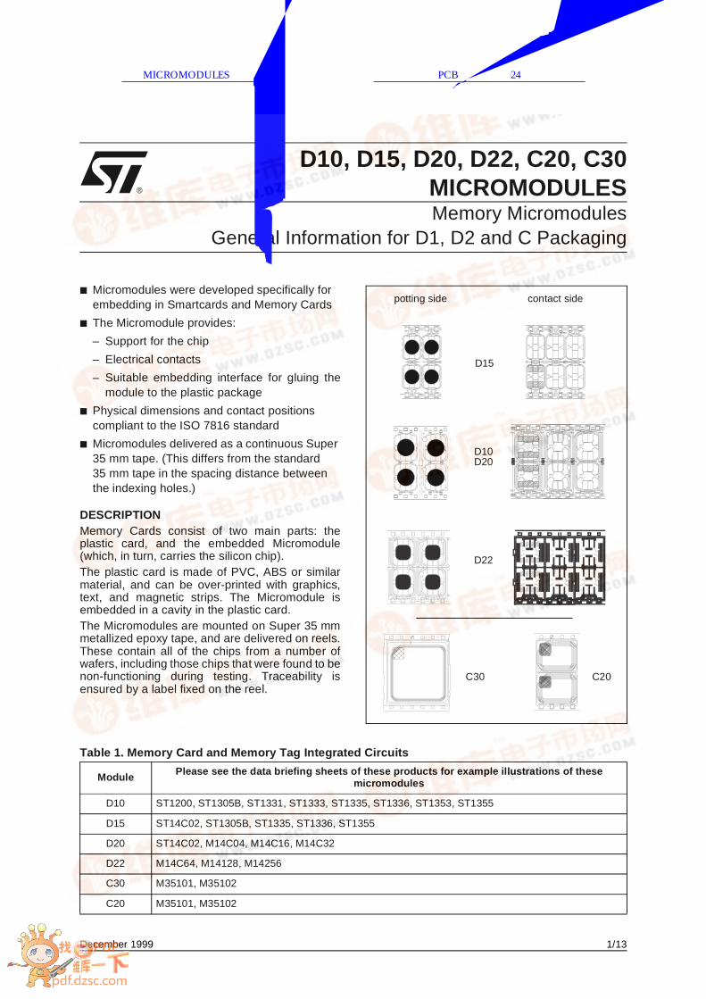
D10, D15, D20, D22, C20, C30MICROMODULESMemory Micromodules
General Information for D1, D2 and C Packaging
Micromodules were developed specifically for embedding in Smartcards and Memory Cards
The Micromodule provides:
– Support for the chip
– Electrical contacts
– Suitable embedding interface for gluing themodule to the plastic package
Physical dimensions and contact positions compliant to the ISO 7816 standard
Micromodules delivered as a continuous Super 35 mm tape. (This differs from the standard 35 mm tape in the spacing distance between the indexing holes.)
DESCRIPTIONMemory Cards consist of two main parts: theplastic card, and the embedded Micromodule(which, in turn, carries the silicon chip).The plastic card is made of PVC, ABS or similarmaterial, and can be over-printed with graphics,text, and magnetic strips. The Micromodule isembedded in a cavity in the plastic card. The Micromodules are mounted on Super 35 mmmetallized epoxy tape, and are delivered on reels.These contain all of the chips from a number ofwafers, including those chips that were found to benon-functioning during testing. Traceability isensured by a label fixed on the reel.
D10D20
11 1
1
11 1
1
potting side contact side
D15
D22
C30 C20
Table 1. Memory Card and Memory Tag Integrated Circuits
Module Please see the data briefing sheets of these products for example illustrations of these micromodules
D10 ST1200, ST1305B, ST1331, ST1333, ST1335, ST1336, ST1353, ST1355
D15 ST14C02, ST1305B, ST1335, ST1336, ST1355
D20 ST14C02, M14C04, M14C16, M14C32
D22 M14C64, M14128, M14256
C30 M35101, M35102
C20 M35101, M35102
查询MICROMODULES 供应商 捷多邦,专业PCB打样工厂,24小时加急出货
2/13
MICROMODULES
The assembly flows is as follows:1. Dice sawing2. Dice attach3. Wire bonding4. Potting5. Milling (depending on product)The range of products and types of Micromoduleare summarized in Table 1 and Table 2. For largevolumes, ST is able to offer customized moduletape.
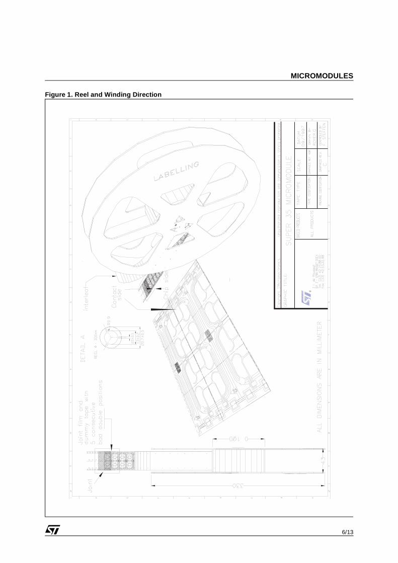
DELIVERYThe Super 35mm metallized epoxy tape isdelivered on reels, as shown in Figure 1. Thesecontain all of the chips from a number of wafers,including those chips that were found to be non-functioning during testing. Traceability is ensuredby a label fixed on the reel.The typical quantity is 10,000 modules per reel,with priority given to lot integrity on the reel. Themaximum quantity is 15,000 per reel.Parts which are faulty (mechanically or electricallydefective) are identified by punch holes. Thespecification for the reject punch holes is shown in
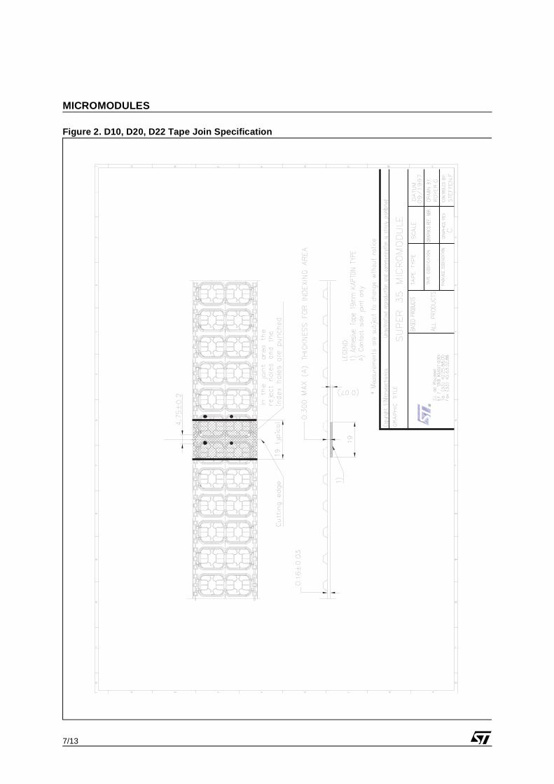
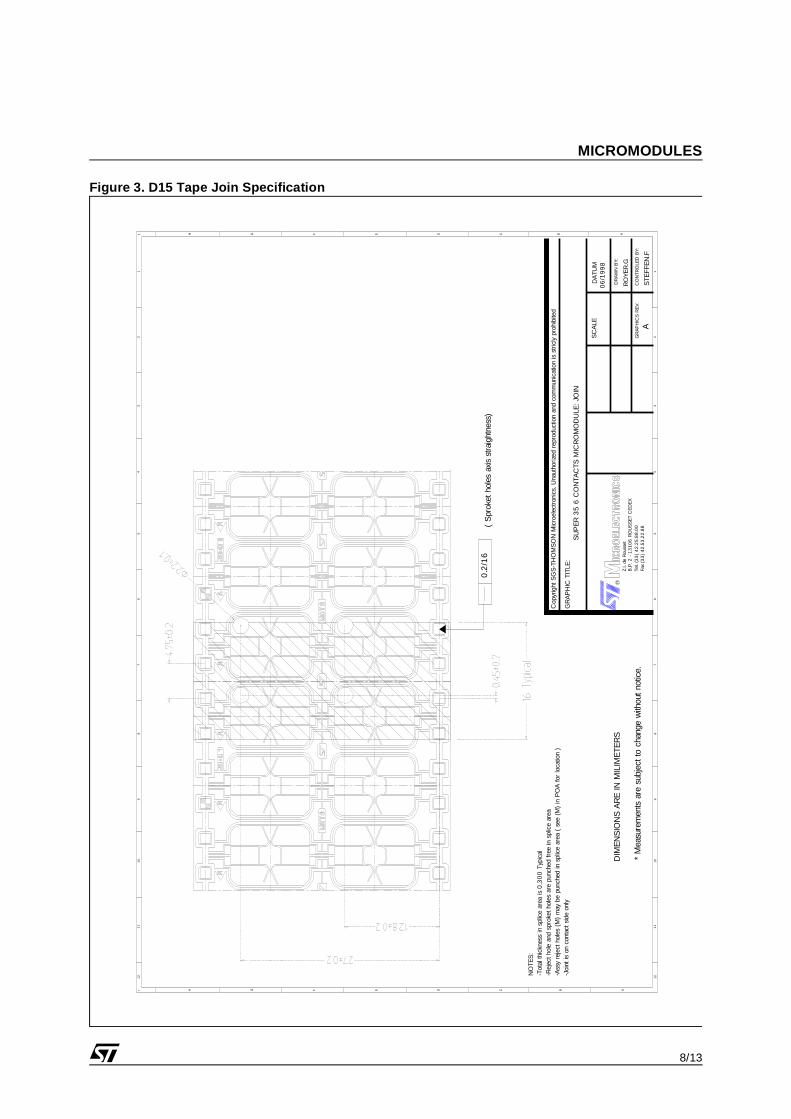
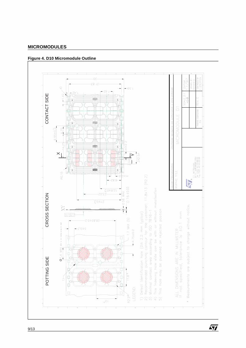
Figure 4 for the D10 micromodule, in Figure 5 forthe D15 micromodule, in Figure 6 for the D20micromodule, and in Figure 7 for the D22micromodule.Tape joins (tape splicing) are never more than 10per 10 metre length, as shown in Figure 2 andFigure 3.At least 2.1 m of leader, and 2.1 m of trailer isincluded on each reel. Each is made of PVC Super35 mm tape, without metalisation, and is opaqueto infrared and white light.A “failure” marking of reject holes is included at thebeginning and end of the tape of a minimum of 5consecutive module pitches (double positions).Modules should be stored within the temperaturerange -40 °C to + 85 °C, for no more than 1 year.Each reel is packed in an antistatic bag, along witha desiccant bag, and a humidity indicator card.This card indicates the level of humidity as follows:
30 - Blue: protection assured40 - Pink: renew the desiccant bag50 - Pink: protection no longer ensured
Three self adhesive plastic identification labels areattached: one to the reel, one to the antistatic bag,
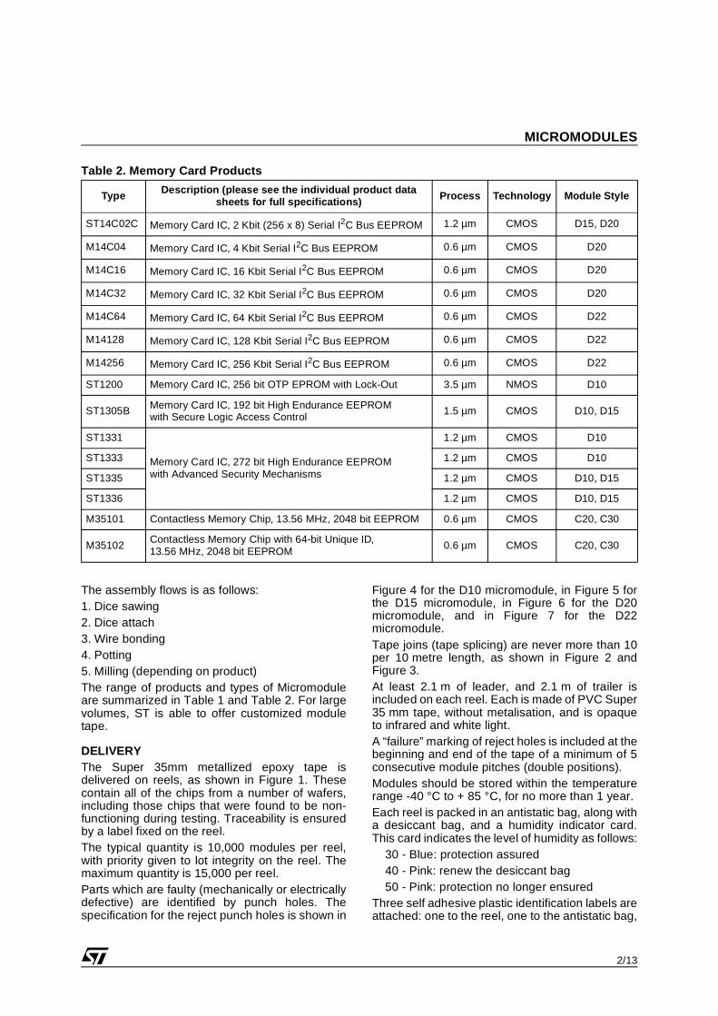
Table 2. Memory Card Products
Type Description (please see the individual product data sheets for full specifications) Process Technology Module Style
ST14C02C Memory Card IC, 2 Kbit (256 x 8) Serial I2C Bus EEPROM 1.2 µm CMOS D15, D20
M14C04 Memory Card IC, 4 Kbit Serial I2C Bus EEPROM 0.6 µm CMOS D20
M14C16 Memory Card IC, 16 Kbit Serial I2C Bus EEPROM 0.6 µm CMOS D20
M14C32 Memory Card IC, 32 Kbit Serial I2C Bus EEPROM 0.6 µm CMOS D20
M14C64 Memory Card IC, 64 Kbit Serial I2C Bus EEPROM 0.6 µm CMOS D22
M14128 Memory Card IC, 128 Kbit Serial I2C Bus EEPROM 0.6 µm CMOS D22
M14256 Memory Card IC, 256 Kbit Serial I2C Bus EEPROM 0.6 µm CMOS D22
ST1200 Memory Card IC, 256 bit OTP EPROM with Lock-Out 3.5 µm NMOS D10
ST1305B Memory Card IC, 192 bit High Endurance EEPROMwith Secure Logic Access Control
1.5 µm CMOS D10, D15
ST1331
Memory Card IC, 272 bit High Endurance EEPROMwith Advanced Security Mechanisms
1.2 µm CMOS D10
ST1333 1.2 µm CMOS D10
ST1335 1.2 µm CMOS D10, D15
ST1336 1.2 µm CMOS D10, D15
M35101 Contactless Memory Chip, 13.56 MHz, 2048 bit EEPROM 0.6 µm CMOS C20, C30
M35102Contactless Memory Chip with 64-bit Unique ID,13.56 MHz, 2048 bit EEPROM
0.6 µm CMOS C20, C30
MICROMODULES
3/13
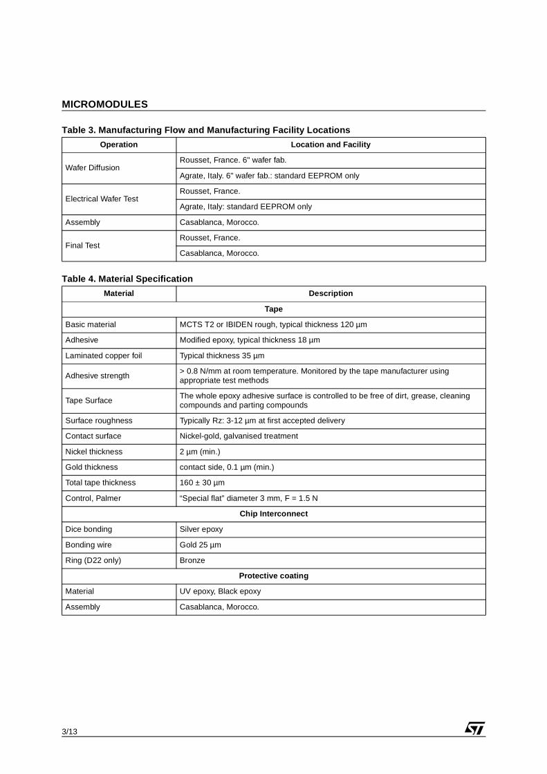
Table 3. Manufacturing Flow and Manufacturing Facility Locations
Table 4. Material Specification
Operation Location and Facility
Wafer Diffusion Rousset, France. 6" wafer fab.
Agrate, Italy. 6" wafer fab.: standard EEPROM only
Electrical Wafer Test Rousset, France.
Agrate, Italy: standard EEPROM only
Assembly Casablanca, Morocco.
Final Test Rousset, France.
Casablanca, Morocco.
Material Description
Tape
Basic material MCTS T2 or IBIDEN rough, typical thickness 120 µm
Adhesive Modified epoxy, typical thickness 18 µm
Laminated copper foil Typical thickness 35 µm
Adhesive strength > 0.8 N/mm at room temperature. Monitored by the tape manufacturer using appropriate test methods
Tape Surface The whole epoxy adhesive surface is controlled to be free of dirt, grease, cleaning compounds and parting compounds
Surface roughness Typically Rz: 3-12 µm at first accepted delivery
Contact surface Nickel-gold, galvanised treatment
Nickel thickness 2 µm (min.)
Gold thickness contact side, 0.1 µm (min.)
Total tape thickness 160 ± 30 µm
Control, Palmer “Special flat” diameter 3 mm, F = 1.5 N
Chip Interconnect
Dice bonding Silver epoxy
Bonding wire Gold 25 µm
Ring (D22 only) Bronze
Protective coating
Material UV epoxy, Black epoxy
Assembly Casablanca, Morocco.
4/13
MICROMODULES
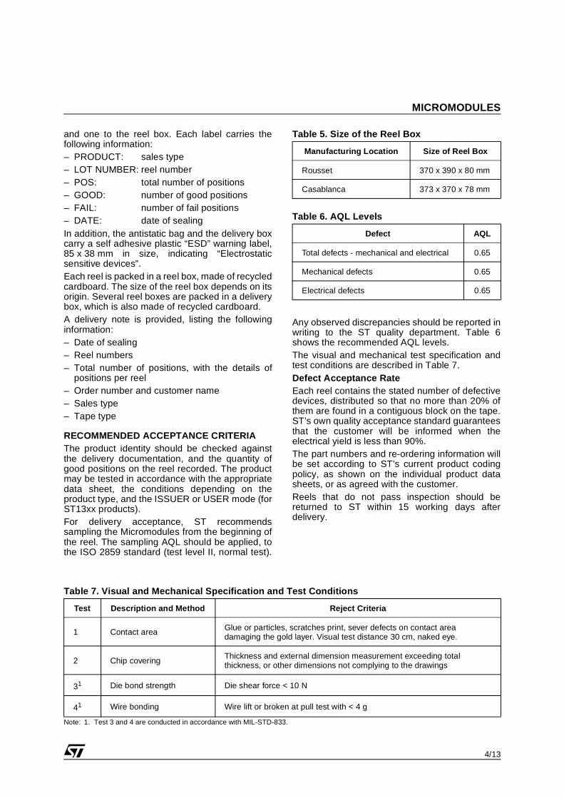
Table 5. Size of the Reel Box
Table 6. AQL Levels
Manufacturing Location Size of Reel Box
Rousset 370 x 390 x 80 mm
Casablanca 373 x 370 x 78 mm
Defect AQL
Total defects - mechanical and electrical 0.65
Mechanical defects 0.65
Electrical defects 0.65
Table 7. Visual and Mechanical Specification and Test Conditions
Note: 1. Test 3 and 4 are conducted in accordance with MIL-STD-833.
Test Description and Method Reject Criteria
1 Contact area Glue or particles, scratches print, sever defects on contact area damaging the gold layer. Visual test distance 30 cm, naked eye.
2 Chip coveringThickness and external dimension measurement exceeding total thickness, or other dimensions not complying to the drawings
31 Die bond strength Die shear force < 10 N
41 Wire bonding Wire lift or broken at pull test with < 4 g
Any observed discrepancies should be reported inwriting to the ST quality department. Table 6shows the recommended AQL levels.The visual and mechanical test specification andtest conditions are described in Table 7.Defect Acceptance RateEach reel contains the stated number of defectivedevices, distributed so that no more than 20% ofthem are found in a contiguous block on the tape.ST’s own quality acceptance standard guaranteesthat the customer will be informed when theelectrical yield is less than 90%.The part numbers and re-ordering information willbe set according to ST’s current product codingpolicy, as shown on the individual product datasheets, or as agreed with the customer.Reels that do not pass inspection should bereturned to ST within 15 working days afterdelivery.
and one to the reel box. Each label carries thefollowing information:– PRODUCT: sales type– LOT NUMBER: reel number– POS: total number of positions– GOOD: number of good positions– FAIL: number of fail positions– DATE: date of sealingIn addition, the antistatic bag and the delivery boxcarry a self adhesive plastic “ESD” warning label,85 x 38 mm in size, indicating “Electrostaticsensitive devices”.Each reel is packed in a reel box, made of recycledcardboard. The size of the reel box depends on itsorigin. Several reel boxes are packed in a deliverybox, which is also made of recycled cardboard.A delivery note is provided, listing the followinginformation:– Date of sealing– Reel numbers– Total number of positions, with the details of
positions per reel– Order number and customer name– Sales type– Tape type
RECOMMENDED ACCEPTANCE CRITERIAThe product identity should be checked againstthe delivery documentation, and the quantity ofgood positions on the reel recorded. The productmay be tested in accordance with the appropriatedata sheet, the conditions depending on theproduct type, and the ISSUER or USER mode (forST13xx products).For delivery acceptance, ST recommendssampling the Micromodules from the beginning ofthe reel. The sampling AQL should be applied, tothe ISO 2859 standard (test level II, normal test).
MICROMODULES
5/13
RELIABILITYProduct qualification and on-going reliabilitymonitoring is performed by ST. The principal stepsare listed in Table 8 and Table 9.
Table 8. Package Related Tests
Note: 1. The notation m/n means: reject the whole lot if more than m devices fail from a sample of n devices. For instance, 0/45 means asample of 45 devices taken from a lot, with the whole lot only accepted if every one of the 45 sample devices passed the test.
Table 9. Product Related Tests
Test Description Method Condition LPTD Criteria (note 1)
1 Geometry ST Specification Monitoring/Lot 5 0/45
2 Visual inspection ST Specification Outgoing/Lot AQL= 0.040 0/315
3 Temperature cycling MIL-STD-883 Method 1010
-40 °C to 150 °C, 100 cycles 5 0/45
4Salt atmosphere corrosion of contacts
MIL-STD-883 Method 1009
35 °C, 5% NaCl, 24 hour 15 0/15
5 Moisture resistance MIL-STD-883 Method 1004
85 °C, 85% HR Biased 5.5 V, 168 hour
7 0/32
6Vibration with electrical measurement
ISO/IEC 103731 octave/minute, acceleration up to 10 G (repeated 20 times)measurement memory check at 25 °C
20 0/11
7 Bending properties ISO/IEC 7816-1Long side: deflection 2 cmShort side: deflection 1 cm30 bendings per minute
20 0/11
8 Torsion properties ISO/IEC 7816-1Maximum displacement 15° ±1°1000 torsions, 30 torsions per minute applied on long side only
20 0/11
Test Description Method Condition LPTD Criteria
1 Life test MIL-STD-883 Method 1005
140 °C, 6 V, 504 hours measurement memory check at 25 °C
3 0/76
2 Electrostatic discharge MIL-STD-883 Method 3015
Human body model:1.5 kΩ, 100 pF, ± 5000 V
n/a 0/9
Electrostatic discharge MIL-STD-883 Method 3015
Machine model: 0 Ω, 200 pF, ± 200 Vmeasurement memory check at 25 °C
n/a 0/9
3 Data retention, Temperature storage
MIL-STD-883 Method 1005
150 °C, 1000 hours, no biasmeasurement memory check at 25 °C
5 0/45
4 Write/Erase cycles ST Specification 100,000 Cycles 200 ppm/1024 byte/1000 cycle
0/32
5 Magnetic field, memory check
ISO IEC 10373 79,500 A/m 15 1/25
6 X-rays, memory check ISO IEC 10373 70 kV, 0.1 Grey 15 1/25
7 UV light, memory check ISO IEC 10373 15 W.s/cm2, 30 minutes maximum 15 1/25
6/13
MICROMODULES
Figure 1. Reel and Winding Direction
MICROMODULES
7/13
Figure 2. D10, D20, D22 Tape Join Specification
8/13
MICROMODULES
* M
easu
rem
ents
are
sub
ject
to c
hang
e w
ithou
t not
ice.
12
A
11
10
BCD
98
7
EFGHI12
11
10
98
7
CD
65
43
EFGH
21
I
SU
PER
35 6
CO
NTA
CTS
MIC
RO
MO
DU
LE: JO
IN
65
43
B
RO
YER
.G
21
06/1
998
A
STE
FFEN
.FA
Cop
yrig
ht S
GS-T
HO
MSO
N M
icro
elec
troni
cs. U
naut
horiz
ed r
epro
duct
ion
and
com
mun
icat
ion
is s
tricl
y pr
ohib
ited
GR
AP
HIC
TIT
LE:
GR
AP
HIC
S R
EV.
SC
ALE
CO
NTR
OLE
D B
Y:
DR
AW
N B
Y:
DATU
M
Z.I.
de R
ouss
et
Fax
(33)
42.5
3.2
2.8
8Te
l. (3
3)
42.2
5.8
8.0
0B
.P. 2
- 1
3106 R
OU
SSET
CED
EX
NO
TES:
-Tot
al th
ickn
ess
in s
plic
e ar
ea is
0.3
00 T
ypic
al-R
ejec
t hol
e an
d sp
roke
t hol
es a
re p
unch
ed fre
e in
spl
ice
area
-Ass
y re
ject
hol
es (
M)
may
be
punc
hed
in s
plic
e ar
ea (
see
(M
) in
PO
A for
loca
tion
)-J
oint
is o
n co
ntac
t sid
e on
ly
DIM
EN
SIO
NS A
RE IN
MIL
IMETE
RS
0.2
/16
( Spr
oket
hol
es a
xis
stra
ight
ness
)
Figure 3. D15 Tape Join Specification
MICROMODULES
9/13
Figure 4. D10 Micromodule Outline
PO
TT
ING
SID
EC
RO
SS
SE
CT
ION
CO
NT
AC
T S
IDE
1 1
11
11
1 1
OX Y
10/13
MICROMODULES
2.6min7.62
2.2
min
2.5
4
35
4.7
5
8.815
23.015
9.5
1.422
1.4
22
R0.15
270.2
12.80.2
5.2
0.2
(P)ø2.2
30.2
(M)ø1.5
7 max
0.1
6
0.5
8 m
ax
0.1
DIE
SID
EC
RO
SS S
EC
TIO
NC
ON
TAC
T SID
E
31.83
Cop
yrig
ht S
GS-T
HO
MSO
N M
icro
elec
troni
cs. U
naut
horiz
ed rep
rodu
ctio
n an
d co
mm
unic
atio
n is s
tricl
y pr
ohib
ited
GR
AP
HIC
TIT
LE:
GR
AP
HIC
S R
EV.
SC
ALE
CO
NTR
OLE
D B
Y:
DR
AW
N B
Y:
DATU
M
Z.I.
de R
ouss
et
Fax
(33)
42.5
3.2
2.8
8Te
l. (3
3)
42.2
5.8
8.0
0B
.P. 2
- 1
3106 R
OU
SSET
CED
EX
PO
A F
OR
MIC
RO
MO
DU
LE D
15
06/1
998
RO
YER
.G
STE
FFEN
.F
none A
NO
TE:
- (P
) is r
ejec
t ide
ntifi
catio
n ho
le ø
2.2
- (M
) m
ay b
e pu
nche
d w
ith (
P): c
ente
r po
sitio
ning
0.2
- Spr
oket
hol
es m
ay b
e w
ith o
r w
ithou
t met
alisat
ion
- R
ecom
men
ded
punc
hing
con
tour
for
the
cust
omer
: 8.3
2*1
1
R1.4
- M
inim
al c
onta
ct a
rea
acco
rdin
g to
ISO
7816-1
GEN
ER
AL
TOLE
RAN
CE IS
0.1
mm
ALL
DIM
EN
SIO
NS A
RE IN
MIL
LIM
ETE
RS
Mea
sure
men
ts a
re s
ubje
ct to
cha
nge
with
out n
otic
eP
AC
KAG
E C
OD
EFU
8.1
2
10.8R1.3
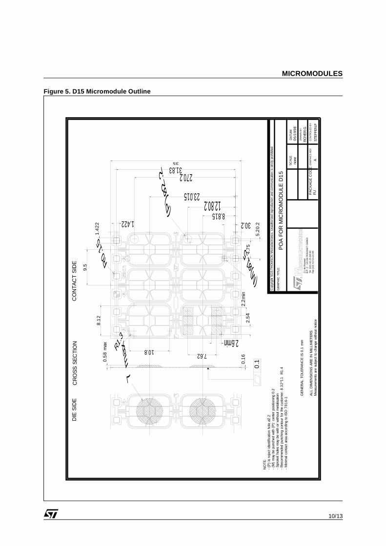
Figure 5. D15 Micromodule Outline
MICROMODULES
11/13
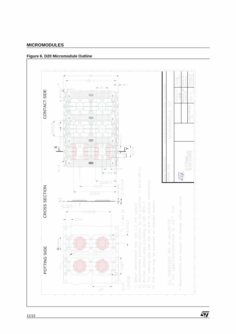
Figure 6. D20 Micromodule Outline
PO
TT
ING
SID
EC
RO
SS
SE
CT
ION
CO
NT
AC
T S
IDE
1 1
11
11
1 1
OX Y
12/13
MICROMODULES
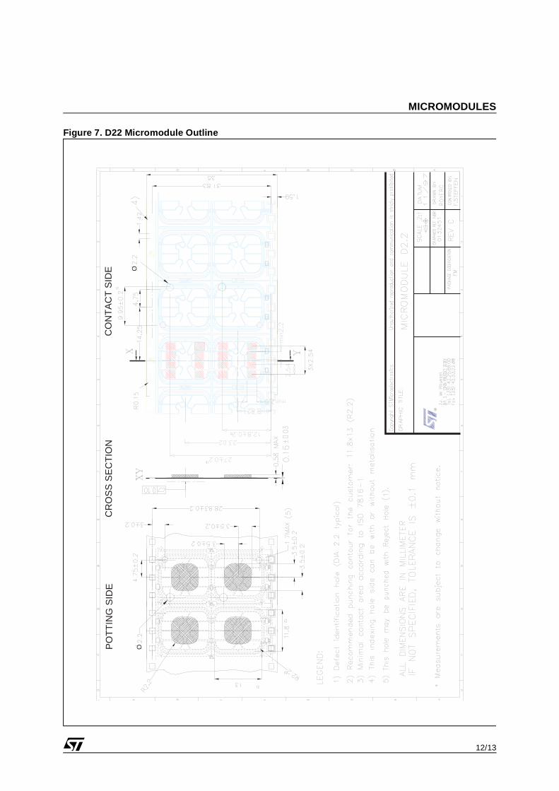
Figure 7. D22 Micromodule Outline
PO
TT
ING
SID
EC
RO
SS
SE
CT
ION
CO
NT
AC
T S
IDE
OO
MICROMODULES
13/13
Information furnished is believed to be accurate and reliable. However, STMicroelectronics assumes no responsibility for the consequencesof use of such information nor for any infringement of patents or other rights of third parties which may result from its use. No license is grantedby implication or otherwise under any patent or patent rights of STMicroelectronics. Specifications mentioned in this publication are subjectto change without notice. This publication supersedes and replaces all information previously supplied. STMicroelectronics products are notauthorized for use as critical components in life support devices or systems without express written approval of STMicroelectronics.
© 1999 STMicroelectronics - All Rights Reserved
The ST logo is a registered trademark of STMicroelectronics.
All other names are the property of their respective owners.
STMicroelectronics GROUP OF COMPANIES
Australia - Brazil - China - Finland - France - Germany - Hong Kong - India - Italy - Japan - Malaysia - Malta - Morocco - Singapore - Spain - Sweden - Switzerland - United Kingdom - U.S.A.
http://www.st.com


![583188000 580669000 Swivel plate MF 580672000 580625000 · [kg] Article n° [kg] Article n° Dam formwork D15 Cantilever bracket D15 K 136.4 580630000 Sperrenkonsole D15 K Cantilever](https://img.pdfslide.net/doc/110x75/5c0cf15909d3f2e4358cf96c/583188000-580669000-swivel-plate-mf-580672000-580625000-kg-article-n-kg.jpg)