Embed Size (px)
Citation preview
10
0 Phase
Detector
Loop
Filter
Variable
Delay
÷2 ÷2
14 bit
2.4Gsps
DAC
10
010
0
Input
RegistersDemux
and
Format
DA_P[13:0]
DA_N[13:0]
DB_P[13:0]
DB_N[13:0]
DLYCLK_P
DLYCLK_N
DTCLK_P
DTCLK_N
DA
CC
LK
_P
DA
CC
LK
_N
Bandgap
Ref
REFIO_IN
REFIO
RBIASOUT
RBIASIN
CSBIAS
CSBIAS_IN
IOUT_P
IOUT_N
LV
DS
_H
TB
INV_CLK
Mode Controls
NO
RM
AL
A_
ON
LY
A_
ON
LY
_IN
V
A_O
NL
Y_
ZS
RESTART
LOCK
SLEEP
10
0 Phase
Detector
Loop
Filter
Variable
Delay
÷2 ÷2
14 bit
2.4Gsps
DAC
10
010
0
Input
RegistersDemux
and
Format
DA_P[13:0]
DA_N[13:0]
DB_P[13:0]
DB_N[13:0]
DLYCLK_P
DLYCLK_N
DTCLK_P
DTCLK_N
DA
CC
LK
_P
DA
CC
LK
_N
Bandgap
Ref
REFIO_IN
REFIO
RBIASOUT
RBIASIN
CSBIAS
CSBIAS_IN
IOUT_P
IOUT_N
LV
DS
_H
TB
INV_CLK
Mode Controls
NO
RM
AL
A_
ON
LY
A_
ON
LY
_IN
V
A_O
NL
Y_
ZS
RESTART
SLEEP
Product
Folder
Sample &Buy
Technical
Documents
Tools &
Software
Support &Community
An IMPORTANT NOTICE at the end of this data sheet addresses availability, warranty, changes, use in safety-critical applications,intellectual property matters and other important disclaimers. PRODUCTION DATA.
DAC5670SGLS394F –MARCH 2010–REVISED MAY 2016
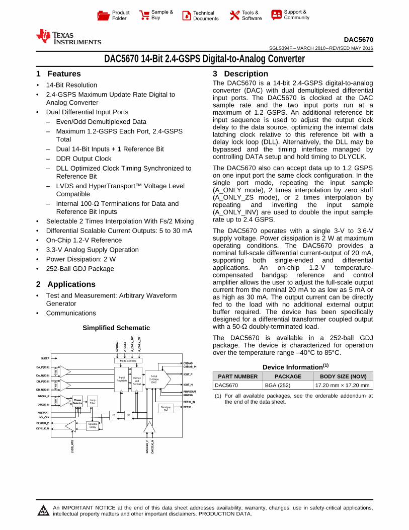
DAC5670 14-Bit 2.4-GSPS Digital-to-Analog Converter
1
1 Features1• 14-Bit Resolution• 2.4-GSPS Maximum Update Rate Digital to
Analog Converter• Dual Differential Input Ports
– Even/Odd Demultiplexed Data– Maximum 1.2-GSPS Each Port, 2.4-GSPS
Total– Dual 14-Bit Inputs + 1 Reference Bit– DDR Output Clock– DLL Optimized Clock Timing Synchronized to
Reference Bit– LVDS and HyperTransport™ Voltage Level
Compatible– Internal 100-Ω Terminations for Data and
Reference Bit Inputs• Selectable 2 Times Interpolation With Fs/2 Mixing• Differential Scalable Current Outputs: 5 to 30 mA• On-Chip 1.2-V Reference• 3.3-V Analog Supply Operation• Power Dissipation: 2 W• 252-Ball GDJ Package
2 Applications• Test and Measurement: Arbitrary Waveform
Generator• Communications
Simplified Schematic
3 DescriptionThe DAC5670 is a 14-bit 2.4-GSPS digital-to-analogconverter (DAC) with dual demultiplexed differentialinput ports. The DAC5670 is clocked at the DACsample rate and the two input ports run at amaximum of 1.2 GSPS. An additional reference bitinput sequence is used to adjust the output clockdelay to the data source, optimizing the internal datalatching clock relative to this reference bit with adelay lock loop (DLL). Alternatively, the DLL may bebypassed and the timing interface managed bycontrolling DATA setup and hold timing to DLYCLK.
The DAC5670 also can accept data up to 1.2 GSPSon one input port the same clock configuration. In thesingle port mode, repeating the input sample(A_ONLY mode), 2 times interpolation by zero stuff(A_ONLY_ZS mode), or 2 times interpolation byrepeating and inverting the input sample(A_ONLY_INV) are used to double the input samplerate up to 2.4 GSPS.
The DAC5670 operates with a single 3-V to 3.6-Vsupply voltage. Power dissipation is 2 W at maximumoperating conditions. The DAC5670 provides anominal full-scale differential current-output of 20 mA,supporting both single-ended and differentialapplications. An on-chip 1.2-V temperature-compensated bandgap reference and controlamplifier allows the user to adjust the full-scale outputcurrent from the nominal 20 mA to as low as 5 mA oras high as 30 mA. The output current can be directlyfed to the load with no additional external outputbuffer required. The device has been specificallydesigned for a differential transformer coupled outputwith a 50-Ω doubly-terminated load.
The DAC5670 is available in a 252-ball GDJpackage. The device is characterized for operationover the temperature range –40°C to 85°C.
Device Information(1)
PART NUMBER PACKAGE BODY SIZE (NOM)DAC5670 BGA (252) 17.20 mm × 17.20 mm
(1) For all available packages, see the orderable addendum atthe end of the data sheet.
2
DAC5670SGLS394F –MARCH 2010–REVISED MAY 2016 www.ti.com
Product Folder Links: DAC5670
Submit Documentation Feedback Copyright © 2010–2016, Texas Instruments Incorporated
Table of Contents1 Features .................................................................. 12 Applications ........................................................... 13 Description ............................................................. 14 Revision History..................................................... 25 Pin Configuration and Functions ......................... 36 Specifications......................................................... 6
6.1 Absolute Maximum Ratings ..................................... 66.2 ESD Ratings.............................................................. 66.3 Recommended Operating Conditions....................... 66.4 Thermal Information .................................................. 76.5 DC Electrical Characteristics .................................... 76.6 AC Electrical Characteristics..................................... 86.7 Digital Electrical Characteristics................................ 96.8 Timing Requirements ................................................ 96.9 Typical Characteristics ............................................ 11
7 Detailed Description ............................................ 137.1 Overview ................................................................. 13
7.2 Functional Block Diagram ....................................... 137.3 Feature Description................................................. 147.4 Device Functional Modes........................................ 22
8 Application and Implementation ........................ 248.1 Application Information............................................ 248.2 Typical Application .................................................. 24
9 Power Supply Recommendations ...................... 2610 Layout................................................................... 26
10.1 Layout Guidelines ................................................. 2610.2 Layout Example .................................................... 26
11 Device and Documentation Support ................. 2711.1 Device Support...................................................... 2711.2 Community Resources.......................................... 2711.3 Trademarks ........................................................... 2711.4 Electrostatic Discharge Caution............................ 2811.5 Glossary ................................................................ 28
12 Mechanical, Packaging, and OrderableInformation ........................................................... 28
4 Revision History
Changes from Revision E (February 2013) to Revision F Page
• Added Handling Ratings table, Feature Description section, Device Functional Modes, Application andImplementation section, Power Supply Recommendations section, Layout section, Device and DocumentationSupport section, and Mechanical, Packaging, and Orderable Information section ............................................................... 1
• Corrected Setup/Hold Data to DLYCLK values to be frequency independent ....................................................................... 9• Updated DLL Usage section................................................................................................................................................. 15
1 2 3 4 5 6 7 8 9 10 11 12 13 1514 16
A GND LOCK GND IOUT_P GND GND IOUT_N GND RBIASOUT GND
B NORMAL AVDD GND IOUT_P AVDD AVDD IOUT_N GND RBIASIN REFIO
REFIO_INC RESTART A_ONLY_ZS GND GND GND GND GND GND
D INV_CLK A_ONLY_INV SLEEP LVDS_HTB A_ONLY
E GND GND GND GND AVDD AVDD AVDD AVDD AVDD AVDD GND
GND
CSCAP_IN
CSCAP
F DACCLK_P DACCLK_N GND AVDD GND GND AVDD AVDD GND GND AVDD
G GND GND GND AVDD GND GND GND GND GND GND AVDD
H GND AVDD AVDD GND / / GND AVDD AVDDDB_N(0)AVDD GND
J GND DA_P(13) DA_N(13) AVDD AVDD GND / / GND AVDD AVDDDB_N(1)AVDD GND
K DA_P(12) DA_N(12) AVDD GND GND GND GND GND GND AVDDDB_P(2)DB_N(2) DB_P(1)
L DA_P(11) DA_N(11) DA_P(10) DA_N(10) AVDD GND GND AVDD AVDD GND GND AVDD DB_N(6) DB_N(3) DB_P(3)
M DA_P(9) DA_N(9) DA_P(8) DA_N(8) GND AVDD AVDD AVDD AVDD AVDD AVDD GND DB_P(6) DB_N(4) DB_P(4)
N
P
R
T
DA_P(7)
DA_P(5)
GND
DA_N(7)
DA_N(5)
DA_P(4)
DA_P(6)
GND
DA_N(4)
DA_P(3)
DA_N(6)
DA_N(3) DA_N(1) DA_N(0)
DA_P(2) DA_P(1) DA_P(0)DA_N(2)
DTCLK_P
DLYCLK_P
AVDD
GND
DTCLK_N
DLYCLK_N
AVDD
GND GND
DB_N(13)
DB_P(13) DB_N(12) DB_N(11) DB_N(10) DB_P(9)
DB_N(7) DB_P(7)
DB_N(5) DB_P(5)
DB_N(9) GND
DB_P(12) DB_P(11) DB_P(10)
DB_N(8) DB_P(8)
AVDD
GND
GND
N/C
GND GND
GND
3
DAC5670www.ti.com SGLS394F –MARCH 2010–REVISED MAY 2016
Product Folder Links: DAC5670
Submit Documentation FeedbackCopyright © 2010–2016, Texas Instruments Incorporated
5 Pin Configuration and Functions
Figure 1. Ball Grid Array of the DAC5670
Pin FunctionsPIN
I/O DESCRIPTIONNAME NO.
DACCLK_P F1 I External clock input; sample clock for the DAC.DACCLK_N F2 I Complementary external clock input; sample clock for the DAC.DLYCLK_P P8 O DDR type data clock output to data source.DLYCLK_N P9 O DDR type data clock output to data source complementary signal.DTCLK_P N8 I Input data toggling reference bit.DTCLK_N N9 I Input data toggling reference bit complementary signal.DA_P[13] J2 I Port A data bit 13 (MSB).DA_N[13] J3 I Port A data bit 13 complement (MSB).DA_P[12] K1 I Port A data bit 12.
4
DAC5670SGLS394F –MARCH 2010–REVISED MAY 2016 www.ti.com
Product Folder Links: DAC5670
Submit Documentation Feedback Copyright © 2010–2016, Texas Instruments Incorporated
Pin Functions (continued)PIN
I/O DESCRIPTIONNAME NO.
DA_N[12] K2 I Port A data bit 12 complement.DA_P[11] L1 I Port A data bit 11.DA_N[11] L2 I Port A data bit 11 complement.DA_P[10] L3 I Port A data bit 10.DA_N[10] L4 I Port A data bit 10 complement.DA_P[9] M1 I Port A data bit 9.DA_N[9] M2 I Port A data bit 9 complement.DA_P[8] M3 I Port A data bit 8.DA_N[8] M4 I Port A data bit 8 complement.DA_P[7] N1 I Port A data bit 7.DA_N[7] N2 I Port A data bit 7 complement.DA_P[6] N3 I Port A data bit 6.DA_N[6] N4 I Port A data bit 6 complement.DA_P[5] R1 I Port A data bit 5.DA_N[5] P2 I Port A data bit 5 complement.DA_P[4] T2 I Port A data bit 4.DA_N[4] R3 I Port A data bit 4 complement.DA_P[3] T3 I Port A data bit 3.DA_N[3] R4 I Port A data bit 3 complement.DA_P[2] T4 I Port A data bit 2.DA_N[2] T5 I Port A data bit 2 complement.DA_P[1] T6 I Port A data bit 1.DA_N[1] R6 I Port A data bit 1 complement.DA_P[0] T7 I Port A data bit 0 (LSB).DA_N[0] R7 I Port A data bit 0 complement (LSB).DB_P[13] R10 Port B data bit 13 (MSB).DB_N[13] P10 I Port B data bit 13 complement (MSB).DB_P[12] T12 I Port B data bit 12.DB_N[12] R11 I Port B data bit 12 complement.DB_P[11] T13 I Port B data bit 11.DB_N[11] R12 I Port B data bit 11 complement.DB_P[10] T14 I Port B data bit 10.DB_N[10] R13 I Port B data bit 10 complement.DB_P[9] R14 I Port B data bit 9.DB_N[9] P13 I Port B data bit 9 complement.DB_P[8] R16 I Port B data bit 8.DB_N[8] R15 I Port B data bit 8 complement.DB_P[7] P16 I Port B data bit 7.DB_N[7] P15 I Port B data bit 7 complement.DB_P[6] M13 I Port B data bit 6.DB_N[6] L13 I Port B data bit 6 complement.DB_P[5] N16 I Port B data bit 5.DB_N[5] N15 I Port B data bit 5 complement.DB_P[4] M16 I Port B data bit 4.DB_N[4] M15 I Port B data bit 4 complement.DB_P[3] L16 I Port B data bit 3.
5
DAC5670www.ti.com SGLS394F –MARCH 2010–REVISED MAY 2016
Product Folder Links: DAC5670
Submit Documentation FeedbackCopyright © 2010–2016, Texas Instruments Incorporated
Pin Functions (continued)PIN
I/O DESCRIPTIONNAME NO.
(1) The DLL LOCK indicator on the current version of the DAC5670 is only partially functional. The lock signal may indicate a DLL lockcondition when no DACCLK signal or DTCLK signal is present.
DB_N[3] L15 I Port B data bit 3 complement.DB_P[2] K15 I Port B data bit 2.DB_N[2] K14 I Port B data bit 2 complement.DB_P[1] K16 I Port B data bit 1.DB_N[1] J15 I Port B data bit 1 complement.DB_P[0] J14 I Port B data bit 0 (LSB).DB_N[0] H15 I Port B data bit 0 complement (LSB).IOUT_P A7, B7 O DAC current output. Full scale when all input bits are set 1.IOUT_N A10, B10 O DAC complementary current output. Full scale when all input bits are 0.RBIASOUT A14 O Rbias resistor current output.RBIASIN B14 I Rbias resistor sense input.CSCAP D16 O Current source bias voltage output.CSCAP_IN E16 I Current source bias voltage sense input.REFIO B16 O Bandgap reference output.REFIO_IN C16 I Bandgap reference sense input.RESTART C2 I Resets DLL when high. Low for DLL operation. High for using external setup/hold timing.LVDS_HTB D6 I DLYCLK_P/N control; lvds mode when high, ht mode when low.
INV_CLK D2 I Inverts the DLL target clocking relationship when high. Low for normal DLL operation. See DLLUsage.
LOCK A2 O DLL lock indicator, constant high when locked. (1)
SLEEP D5 I Active high sleep.NORMAL B2 I High for a0,b0,a1,b1,a2,b2, … normal mode.A_ONLY D7 I High for a0,a0,a1,a1,a2,a2, … A_only mode.A_ONLY_INV D4 I High for a0,-a0, a1,-a1,a2,-a2, ... A_only_inv mode.A_ONLY_ZS C3 I High for a0,0,a1,0,a2,0, … A_only_zs mode.
Pin FunctionsPIN
DESCRIPTIONNAME NO.
GND
A1, A6, A8, A9, A11, A16, B6, B11, C6, C7, C8, C9, C10, C11,C14, E1, E2, E3, E5, E12, F3, F4, F6, F7, F10, F11, G1, G2, G3,G4, G6, G7, G8, G9, G10, G11, H1, H7,H10, H16, J1, J7, J10,J16, K6, K7, K8, K9, K10, K11, L6, L7, L10, L11, M5, M12, P3,
P14, T1, T8, T9, T16
Ground.
AVDDB3, B8, B9, C1, E6, E7, E8, E9, E10, E11, F5, F8, F9, F12, G5,
G12, H5, H6, H11, H12, H14, J5, J6, J11, J12, K5, K12, L5, L8, L9,L12, M6, M7, M8, M9, M10, M11, R8, R9
3.3-V analog power supply.
No connect
A3, A4, A13, A15, B1, B4, B13, B15, C4, C12, C13, C15, D3, D8,D9, D10, D11, D12, D13, D14, D15, E4, E13, E14, E15, F13, F14,F15, F16, G13, G14, G15, G16, H2, H3, H4, H13, J4, J13, K3, K4,K13, L14, M14, N5, N6, N7, N10, N11, N12, N13, N14, P1, P4, P5,
P6, P7,P11, P12, R2, R5, T10, T11, T15
No internal connection. These balls can be connectedto GND (if desired), or left open.
No connect B12, C5, D1 Factory use only, must be left unconnected.Reserved A5, A12, B5 Factory use only, must be connected to GND.
6
DAC5670SGLS394F –MARCH 2010–REVISED MAY 2016 www.ti.com
Product Folder Links: DAC5670
Submit Documentation Feedback Copyright © 2010–2016, Texas Instruments Incorporated
(1) Stresses above those listed under Absolute Maximum Ratings may cause permanent damage to the device. Exposure to absolutemaximum conditions for extended periods may degrade device reliability. These are stress ratings only, and functional operation of thedevice at these or any other conditions beyond those indicated under Recommended Operating Conditions is not implied. Exposure toabsolute-maximum-rated conditions for extended periods may affect device reliability.
6 Specifications
6.1 Absolute Maximum Ratingsover operating free-air temperature range (unless otherwise noted) (1)
MIN MAX UNITSupply voltage AVDD to GND 5 VDA_P[13..0], DA_N[13..0], DB_P[13..0], DB_N[13..0] Measured with respect to GND –0.3 AVDD + 0.3 VNORMAL, A_ONLY, A_ONLY_INV, A_ONLY_ZS Measured with respect to GND –0.3 AVDD + 0.3 VDTCLK_P, DTCLK_N, DACCLK_P, DACCLK_N Measured with respect to GND –0.3 AVDD + 0.3 VLVDS_HTB, INV_CLK, RESTART Measured with respect to GND –0.3 AVDD + 0.3 VIOUT_P, IOUT_N Measured with respect to GND AVDD – 0.5 AVDD + 1.5 VCSCAP_IN, REFIO_IN, RBIAS_IN Measured with respect to GND –0.3 AVDD + 0.3 VPeak input current (any input) 20 mAMaximum junction temperature 150 °CLead temperature 1.6 mm (1/16 inch) from the case for 10 s 260 °C
Tstg Storage temperature –65 150 °C
(1) JEDEC document JEP155 states that 500-V HBM allows safe manufacturing with a standard ESD control process.(2) JEDEC document JEP157 states that 250-V CDM allows safe manufacturing with a standard ESD control process.
6.2 ESD RatingsVALUE UNIT
V(ESD)Electrostaticdischarge
Human body model (HBM), per ANSI/ESDA/JEDEC JS-001, all pins (1) ±250 VCharged device model (CDM), per JEDEC specification JESD22-C101, all pins (2) ±250 V
6.3 Recommended Operating Conditionsover operating free-air temperature range (unless otherwise noted)
MIN NOM MAX UNITGENERAL PARAMETERS
Full-scale output current 30 mAVREFIO Input voltage 1.14 1.2 1.26 VAVDD Analog supply voltage 3 3.3 3.6 VCMOS INTERFACE (SLEEP, RESTART, INV_CLK, NORMAL, A_ONLY, A_ONLY_INV, A_ONLY_ZS)VIH High-level input voltage 2 3 VVIL Low-level input voltage 0 0 0.8 VDIFFERENTIAL DATA INTERFACE (DA_P[13:0], DA_N[13:0], DB_P[13:0], DB_N[13:0], DTCLK_P, DTCLK_N)VITH Differential input threshold –100 100 mVVICOM Input common mode 0.6 1.4 VCLOCK INPUTS (DACCLK_P, DACCLK_N)|DACCLK_P–DACCLK_N|
Clock differential input voltage 200 1000 mV
Clock duty cycle 40% 60%VCLKCM Clock common mode 1 1.4 V
7
DAC5670www.ti.com SGLS394F –MARCH 2010–REVISED MAY 2016
Product Folder Links: DAC5670
Submit Documentation FeedbackCopyright © 2010–2016, Texas Instruments Incorporated
(1) For more information about traditional and new thermal metrics, see the IC Package Thermal Metrics application report, SPRA953.(2) Non-thermally enhanced JEDEC standard PCB, per JESD-51, 51-3.(3) MIL-STD-883 test method 1012.
6.4 Thermal Information
THERMAL METRIC (1)DAC5670
UNITGDJ252 PINS
RθJA Junction-to-ambient thermal resistance (2) 22.5 °C/WRθJC Junction-to-case thermal resistance (3) 7.6 °C/W
(1) Typicals are characterization values at 25°C and AVDD = 3.3 V. These parameters are characterized, but not production tested.(2) Specified by design.
6.5 DC Electrical CharacteristicsTC,MIN = –40°C to TC,MAX = 85°C, typical values at 25°C, AVDD = 3 to 3.6 V, IoutFS = 20 mA (unless otherwise noted)
PARAMETER TEST CONDITIONS MIN TYP (1) MAX UNITResolution 14 bits
DC ACCURACYINL Integral nonlinearity TC,MIN to TC,MAX , ƒDAC = 640 MHz,
ƒOUT = 10 MHz–7.5 ±1.5 7.5 LSB
DNL Differential nonlinearity –0.98 ±0.8 1.75Monotonocity 14 bits
ANALOG OUTPUTOffset error Mid code offset –0.45 ±0.09 0.45 %FSRGain error With external reference –6 ±1.6 6 %FSRGain error With internal reference –6 ±1.6 6 %FSR
Output compliance range IO(FS) = 20 mA,AVDD = 3.15 to 3.45 V AVDD – 0.5 AVDD + 0.5 V
Output resistance 300 (2) kΩOutput capacitance IOUT_P and IOUT_N single ended 13.7 (2) pF
REFERENCE OUTPUTReference voltage 1.14 1.2 1.26 VReference output current 100 nA
REFERENCE INPUTInput resistance 1 (2) MΩSmall-signal bandwidth 1.4 MHzInput capacitance 3.2 (2) pF
TEMPERATURE COEFFICIENTSOffset drift 75 ppm of FSR/°CGain drift With external reference 75 ppm of FSR/°CGain drift With internal reference 75 ppm of FSR/°CReference voltage drift 35 ppm/°C
POWER SUPPLYAVDD Analog supply voltage 3 3.3 3.6 VIAVDD Analog supply current ƒDAC = 2.4 GHz, normal input mode 560 650 mA
IAVDDSleep mode, AVDD supplycurrent Sleep mode (SLEEP pin high) 150 180 mA
P Power dissipation ƒDAC = 2.4 GHz, normal input mode 1800 2350 mWPSRR Power-supply rejection ratio AVDD = 3.15 to 3.45 V 0.4 1.3 %FSR/V
8
DAC5670SGLS394F –MARCH 2010–REVISED MAY 2016 www.ti.com
Product Folder Links: DAC5670
Submit Documentation Feedback Copyright © 2010–2016, Texas Instruments Incorporated
(1) Typicals are characterization values at 25°C and AVDD = 3.3 V. These parameters are characterized, but not production tested.
6.6 AC Electrical CharacteristicsTC,MIN = –40°C to TC,MAX = 85°C, typical values at 25°C, AVDD = 3 to 3.6 V, IoutFS = 20 mA (unless otherwise noted)
PARAMETER TEST CONDITIONS MIN TYP (1) MAX UNITANALOG OUTPUTƒDAC Output update rate 2.4 GSPSts(DAC) Output setting time to
0.1% Midscale transition 3.5 ns
tpd Output propagation delay 7 DACCLK+ 1.5 ns
tr(IOUT) Output rise time, 10% to90% 280 ps
tf(IOUT) Output fall time, 90% to10% 280 ps
AC PERFORMANCE
SFDR Spurious-free dynamicrange
ƒDAC = 2.4 GSPS, ƒOUT = 100 MHz, dual-portmode, 0 dBFS 47 55 dBc
ƒDAC = 2.4 GSPS, ƒOUT = 200 MHz, dual-portmode, 0 dBFS 38 51 dBc
ƒDAC = 2.4 GSPS, ƒOUT = 300 MHz, dual-portmode, 0 dBFS 37 41 dBc
ƒDAC = 2.4 GSPS, ƒOUT = 500 MHz, dual-portmode, 0 dBFS 44 50 dBc
ƒDAC = 2.4 GSPS, ƒOUT = 500 MHz, dual-portmode, –6 dBFS 47 dBc
SNR Signal-to-noise ratio
ƒDAC = 2.4 GSPS, ƒOUT = 100 MHz, dual-portmode, 0 dBFS 63 70 dBc
ƒDAC = 2.4 GSPS, ƒOUT = 200 MHz, dual-portmode, 0 dBFS 62 70 dBc
ƒDAC = 2.4 GSPS, ƒOUT = 300 MHz, dual-portmode, 0 dBFS 57 62 dBc
ƒDAC = 2.4 GSPS, ƒOUT = 500 MHz, dual-portmode, 0 dBFS 53 60 dBc
ƒDAC = 2.4 GSPS, ƒOUT = 500 MHz, dual-portmode, –6 dBFS 52 dBc
THD Total harmonic distortion
ƒDAC = 2.4 GSPS, ƒOUT = 100 MHz, dual-portmode, 0 dBFS 50 55 dBc
ƒDAC = 2.4 GSPS, ƒOUT = 200 MHz, dual-portmode, 0 dBFS 41 50 dBc
ƒDAC = 2.4 GSPS, ƒOUT = 300 MHz, dual-portmode, 0 dBFS 38 48 dBc
ƒDAC = 2.4 GSPS, ƒOUT = 500 MHz, dual-portmode, 0 dBFS 47 53 dBc
ƒDAC = 2.4 GSPS, ƒOUT = 500 MHz, dual-portmode, –6 dBFS 44 dBc
IMD3 Third-order two-toneintermodulation
ƒDAC = 2.4 GSPS, ƒOUT = 99 MHz and 102 MHz,each tone at –6 dBFS, dual-port mode 65 70 dBc
ƒDAC = 2.4 GSPS, ƒOUT = 200 MHz and 202MHz, each tone at –6 dBFS, dual-port mode 51 68 dBc
ƒDAC = 2.4 GSPS, ƒOUT = 253 Mhz and 257MHz, each tone at –6 dBFS, dual-port mode 47 57 dBc
ƒDAC = 2.4 GSPS, ƒOUT = 299 Mhz and 302MHz, each tone at –6 dBFS, dual-port mode 51 55 dBc
IMD Four-tone intermodulationƒDAC = 2.4 GSPS, ƒOUT = 298 MHz, 299 MHz,300 MHz, and 301 MHz, each tone at –12 dBFS,dual-port mode
51 62.5 dBc
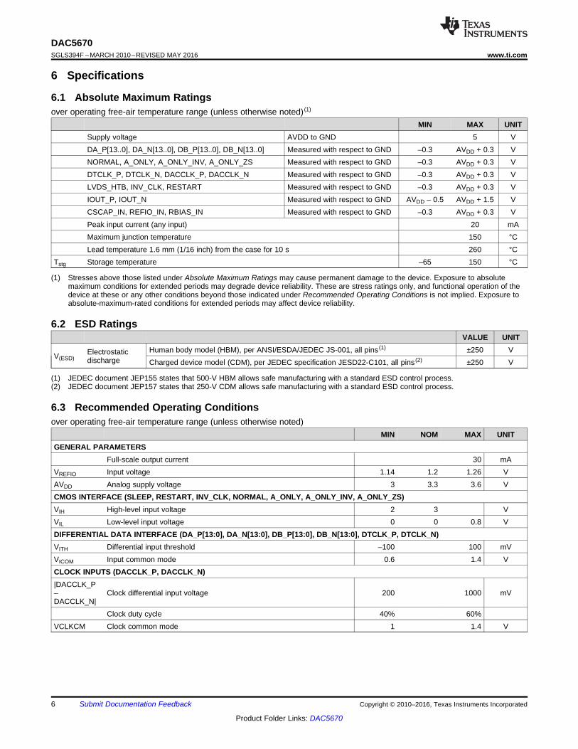
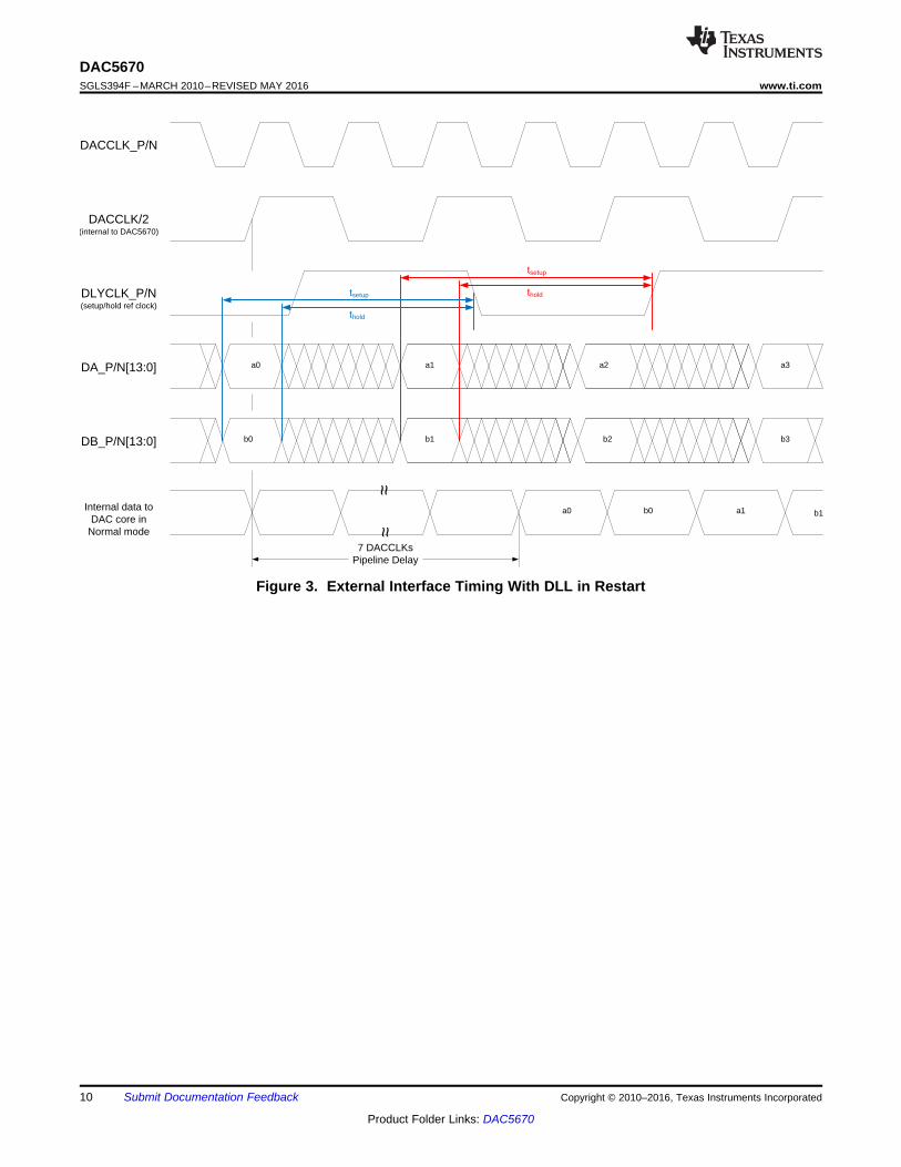
DACLK_P/N
DACCLK/2 internaltoDAC5670
DLYCLK_P/N
DTCLK_P/N
DA_P/N[13:0]
DB_P/N[13:0]
internal data tothe DAC core inNORMAL mode
a0 a1 a2 a3
b3b2b1b0
a0 b0 a1 b1
This internal DACCLK/2 is used to clock the input data DA and DB into theDAC5670
DLYCLK is DACCLK/4 delayed by the DAC5670 DLL to be used as the DDR clock for the data source digital chip
DTCLK is a toggling bit, aligned with DA and DB data from chip, used by the DAC5670 DLL feedback path
7 DACCLKsPipeline Delay
9
DAC5670www.ti.com SGLS394F –MARCH 2010–REVISED MAY 2016
Product Folder Links: DAC5670
Submit Documentation FeedbackCopyright © 2010–2016, Texas Instruments Incorporated
(1) Typicals are characterization values at 25°C and AVDD = 3.3 V. These parameters are characterized, but not production tested.(2) Specified by design.
6.7 Digital Electrical CharacteristicsTC,MIN = –40°C to TC,MAX = 85°C, typical values at 25°C, AVDD = 3 to 3.6 V, IoutFS = 20 mA (unless otherwise noted)
PARAMETER TEST CONDITIONS MIN TYP (1) MAX UNITCMOS INTERFACE (SLEEP, RESTART, INV_CLK, NORMAL, A_ONLY, A_ONLY_INV, A_ONLY_ZS)IIH High-level input current 0.2 10 μAIIL Low-level input current –10 –0.2 μA
Input capacitance 2.5 (2) pFDIFFERENTIAL DATA INTERFACE (DA_P[13:0], DA_N[13:0], DB_P[13:0], DB_N[13:0], DTCLK_P, DTCLK_N)ZT Internal termination impedance 80 100 125 ΩCi Input capacitance 2.6 (2) pF
(1) Tested using SNR as pass/fail criteria.
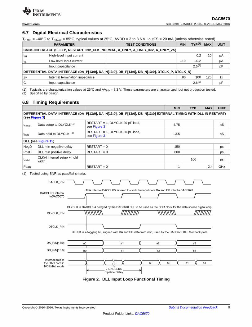
6.8 Timing RequirementsMIN TYP MAX UNIT
DIFFERENTIAL DATA INTERFACE (DA_P[13:0], DA_N[13:0], DB_P[13:0], DB_N[13:0] EXTERNAL TIMING WITH DLL IN RESTART)(see Figure 3)
tsetup Data setup to DLYCLK (1) RESTART = 1, DLYCLK 20-pF load,see Figure 3 4.75 nS
thold Data hold to DLYCLK (1) RESTART = 1, DLYCLK 20-pF load,see Figure 3 –3.5 nS
DLL (see Figure 15)NegD DLL min negative delay RESTART = 0 150 psPosD DLL min positive delay RESTART = 0 600 ps
tvalidCLK/4 internal setup + holdwidth 160 ps
Fdac RESTART = 0 1 2.4 GHz
Figure 2. DLL Input Loop Functional Timing
DACCLK_P/N
DACCLK/2 (internal to DAC5670)
DLYCLK_P/N (setup/hold ref clock)
DA_P/N[13:0]
DB_P/N[13:0]
Internal data to DAC core in
Normal mode
tsetup
thold
a0 a1 a2 a3
b0 b1 b2 b3
a0 b0 a1 b1~ ~
~ ~
7 DACCLKsPipeline Delay
tsetup
thold
10
DAC5670SGLS394F –MARCH 2010–REVISED MAY 2016 www.ti.com
Product Folder Links: DAC5670
Submit Documentation Feedback Copyright © 2010–2016, Texas Instruments Incorporated
Figure 3. External Interface Timing With DLL in Restart
11
DAC5670www.ti.com SGLS394F –MARCH 2010–REVISED MAY 2016
Product Folder Links: DAC5670
Submit Documentation FeedbackCopyright © 2010–2016, Texas Instruments Incorporated
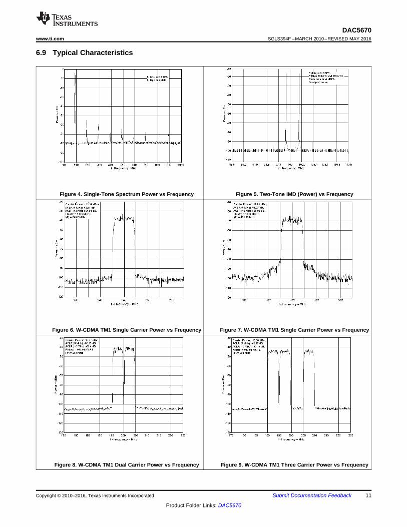
6.9 Typical Characteristics
Figure 4. Single-Tone Spectrum Power vs Frequency Figure 5. Two-Tone IMD (Power) vs Frequency
Figure 6. W-CDMA TM1 Single Carrier Power vs Frequency Figure 7. W-CDMA TM1 Single Carrier Power vs Frequency
Figure 8. W-CDMA TM1 Dual Carrier Power vs Frequency Figure 9. W-CDMA TM1 Three Carrier Power vs Frequency
12
DAC5670SGLS394F –MARCH 2010–REVISED MAY 2016 www.ti.com
Product Folder Links: DAC5670
Submit Documentation Feedback Copyright © 2010–2016, Texas Instruments Incorporated
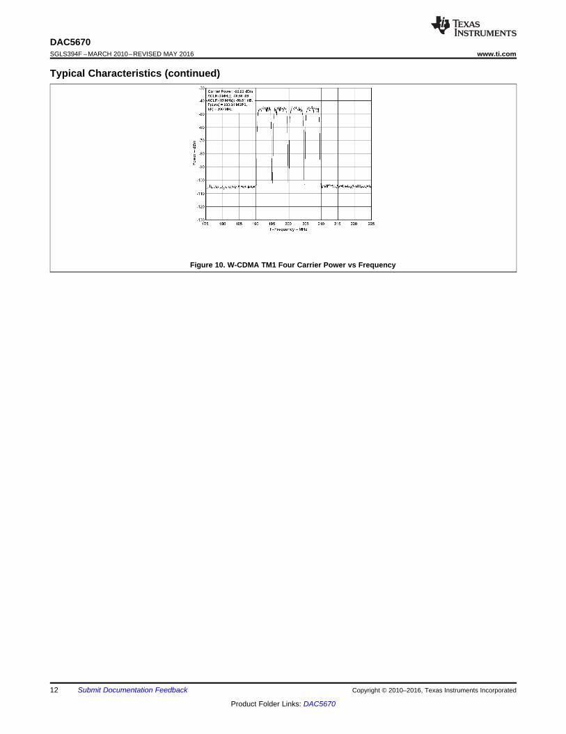
Typical Characteristics (continued)
Figure 10. W-CDMA TM1 Four Carrier Power vs Frequency
10
0 Phase
Detector
Loop
Filter
Variable
Delay
÷2 ÷2
14 bit
2.4Gsps
DAC
10
010
0
Input
RegistersDemux
and
Format
DA_P[13:0]
DA_N[13:0]
DB_P[13:0]
DB_N[13:0]
DLYCLK_P
DLYCLK_N
DTCLK_P
DTCLK_N
DA
CC
LK
_P
DA
CC
LK
_N
Bandgap
Ref
REFIO_IN
REFIO
RBIASOUT
RBIASIN
CSBIAS
CSBIAS_IN
IOUT_P
IOUT_N
LV
DS
_H
TB
INV_CLK
Mode Controls
NO
RM
AL
A_
ON
LY
A_
ON
LY
_IN
V
A_O
NL
Y_
ZS
RESTART
LOCK
SLEEP
10
0 Phase
Detector
Loop
Filter
Variable
Delay
÷2 ÷2
14 bit
2.4Gsps
DAC
10
010
0
Input
RegistersDemux
and
Format
DA_P[13:0]
DA_N[13:0]
DB_P[13:0]
DB_N[13:0]
DLYCLK_P
DLYCLK_N
DTCLK_P
DTCLK_N
DA
CC
LK
_P
DA
CC
LK
_N
Bandgap
Ref
REFIO_IN
REFIO
RBIASOUT
RBIASIN
CSBIAS
CSBIAS_IN
IOUT_P
IOUT_N
LV
DS
_H
TB
INV_CLK
Mode Controls
NO
RM
AL
A_
ON
LY
A_
ON
LY
_IN
V
A_O
NL
Y_
ZS
RESTART
LOCK
SLEEP
13
DAC5670www.ti.com SGLS394F –MARCH 2010–REVISED MAY 2016
Product Folder Links: DAC5670
Submit Documentation FeedbackCopyright © 2010–2016, Texas Instruments Incorporated
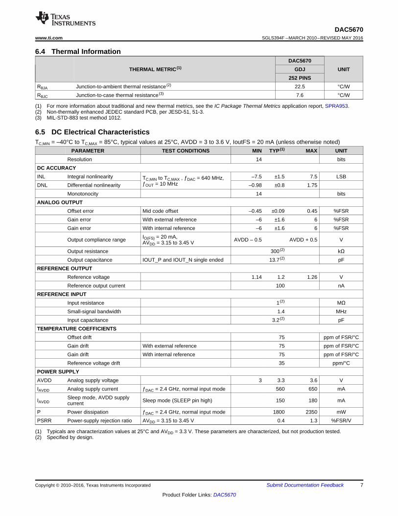
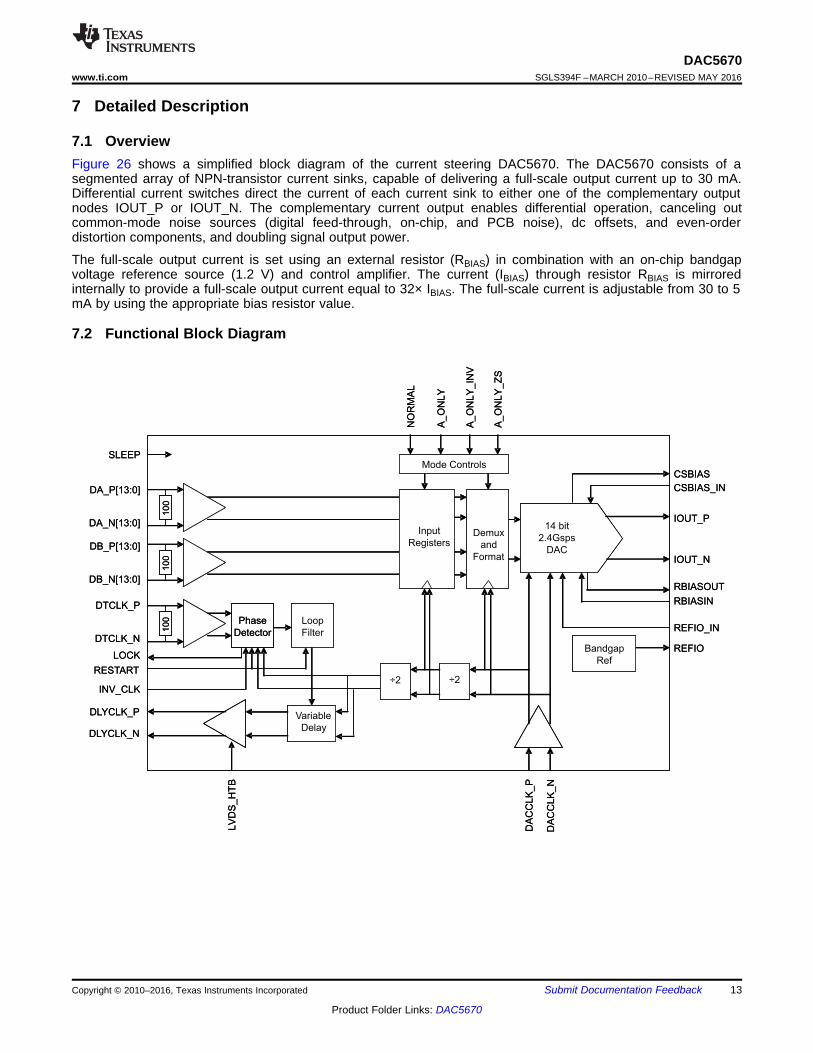
7 Detailed Description
7.1 OverviewFigure 26 shows a simplified block diagram of the current steering DAC5670. The DAC5670 consists of asegmented array of NPN-transistor current sinks, capable of delivering a full-scale output current up to 30 mA.Differential current switches direct the current of each current sink to either one of the complementary outputnodes IOUT_P or IOUT_N. The complementary current output enables differential operation, canceling outcommon-mode noise sources (digital feed-through, on-chip, and PCB noise), dc offsets, and even-orderdistortion components, and doubling signal output power.
The full-scale output current is set using an external resistor (RBIAS) in combination with an on-chip bandgapvoltage reference source (1.2 V) and control amplifier. The current (IBIAS) through resistor RBIAS is mirroredinternally to provide a full-scale output current equal to 32× IBIAS. The full-scale current is adjustable from 30 to 5mA by using the appropriate bias resistor value.
7.2 Functional Block Diagram
14
DAC5670SGLS394F –MARCH 2010–REVISED MAY 2016 www.ti.com
Product Folder Links: DAC5670
Submit Documentation Feedback Copyright © 2010–2016, Texas Instruments Incorporated
7.3 Feature Description
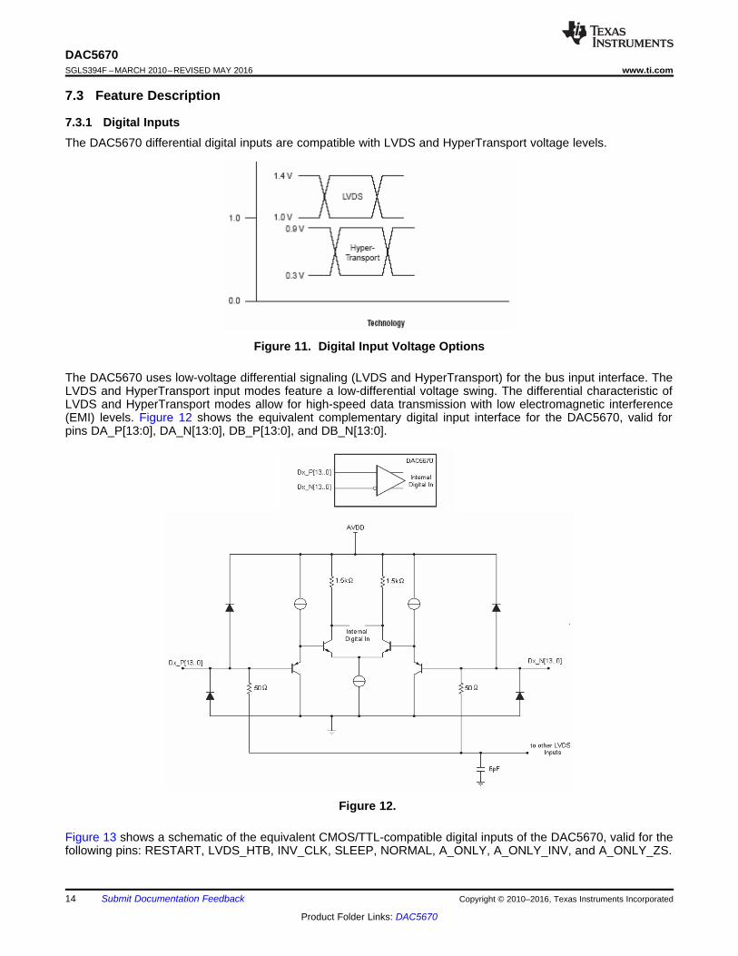
7.3.1 Digital InputsThe DAC5670 differential digital inputs are compatible with LVDS and HyperTransport voltage levels.
Figure 11. Digital Input Voltage Options
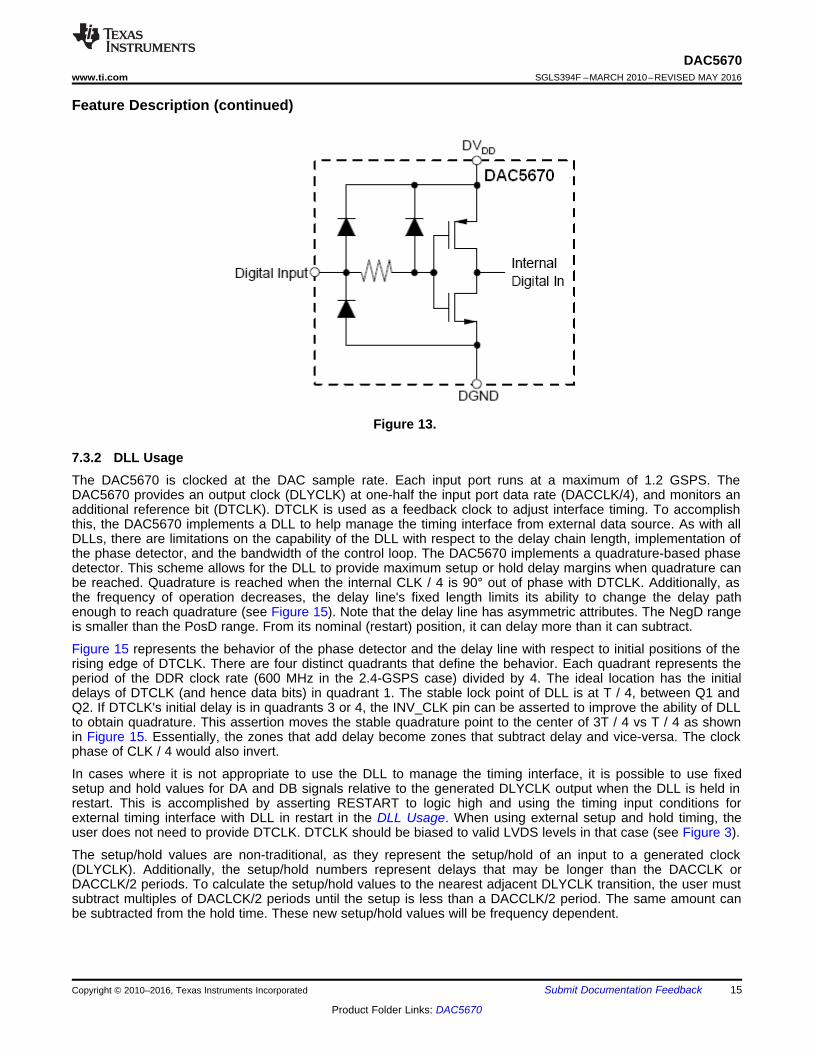
The DAC5670 uses low-voltage differential signaling (LVDS and HyperTransport) for the bus input interface. TheLVDS and HyperTransport input modes feature a low-differential voltage swing. The differential characteristic ofLVDS and HyperTransport modes allow for high-speed data transmission with low electromagnetic interference(EMI) levels. Figure 12 shows the equivalent complementary digital input interface for the DAC5670, valid forpins DA_P[13:0], DA_N[13:0], DB_P[13:0], and DB_N[13:0].
Figure 12.
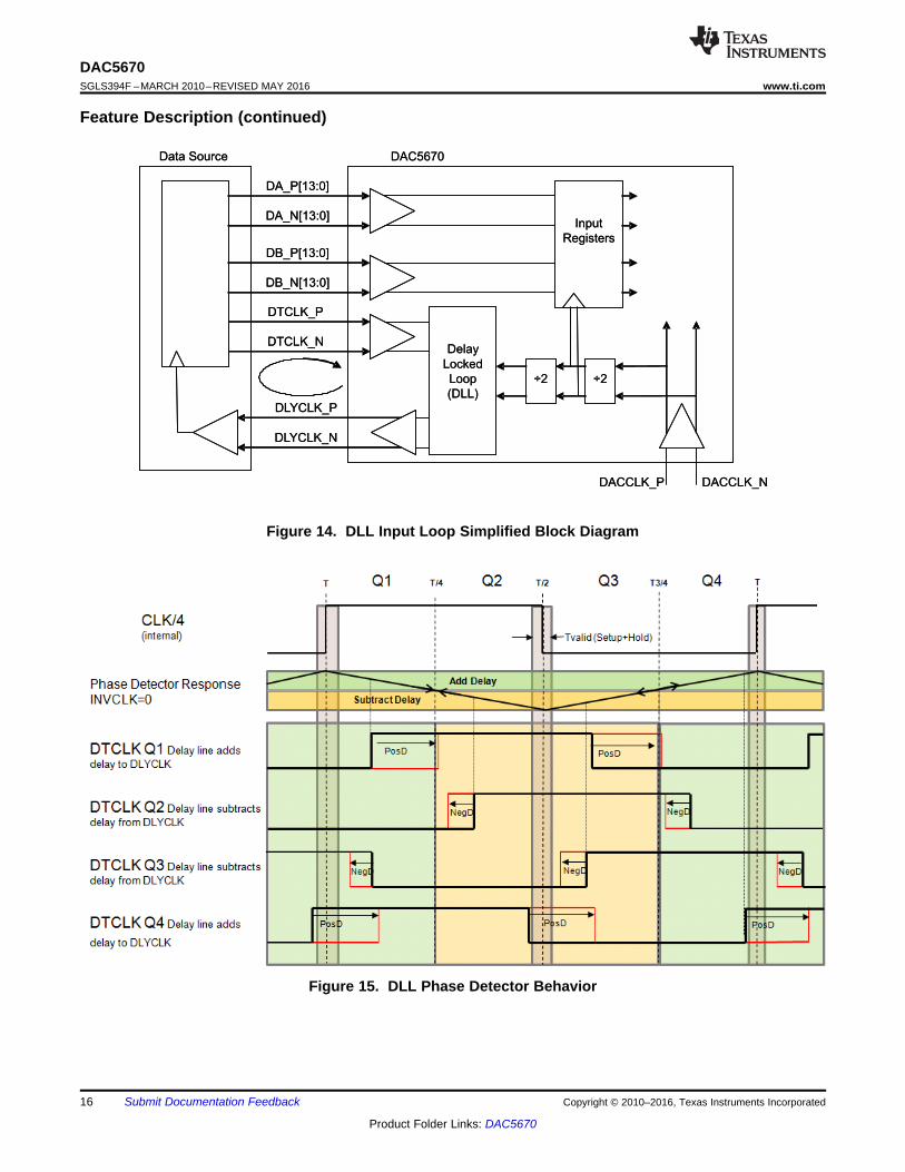
Figure 13 shows a schematic of the equivalent CMOS/TTL-compatible digital inputs of the DAC5670, valid for thefollowing pins: RESTART, LVDS_HTB, INV_CLK, SLEEP, NORMAL, A_ONLY, A_ONLY_INV, and A_ONLY_ZS.
15
DAC5670www.ti.com SGLS394F –MARCH 2010–REVISED MAY 2016
Product Folder Links: DAC5670
Submit Documentation FeedbackCopyright © 2010–2016, Texas Instruments Incorporated
Feature Description (continued)
Figure 13.
7.3.2 DLL UsageThe DAC5670 is clocked at the DAC sample rate. Each input port runs at a maximum of 1.2 GSPS. TheDAC5670 provides an output clock (DLYCLK) at one-half the input port data rate (DACCLK/4), and monitors anadditional reference bit (DTCLK). DTCLK is used as a feedback clock to adjust interface timing. To accomplishthis, the DAC5670 implements a DLL to help manage the timing interface from external data source. As with allDLLs, there are limitations on the capability of the DLL with respect to the delay chain length, implementation ofthe phase detector, and the bandwidth of the control loop. The DAC5670 implements a quadrature-based phasedetector. This scheme allows for the DLL to provide maximum setup or hold delay margins when quadrature canbe reached. Quadrature is reached when the internal CLK / 4 is 90° out of phase with DTCLK. Additionally, asthe frequency of operation decreases, the delay line's fixed length limits its ability to change the delay pathenough to reach quadrature (see Figure 15). Note that the delay line has asymmetric attributes. The NegD rangeis smaller than the PosD range. From its nominal (restart) position, it can delay more than it can subtract.
Figure 15 represents the behavior of the phase detector and the delay line with respect to initial positions of therising edge of DTCLK. There are four distinct quadrants that define the behavior. Each quadrant represents theperiod of the DDR clock rate (600 MHz in the 2.4-GSPS case) divided by 4. The ideal location has the initialdelays of DTCLK (and hence data bits) in quadrant 1. The stable lock point of DLL is at T / 4, between Q1 andQ2. If DTCLK's initial delay is in quadrants 3 or 4, the INV_CLK pin can be asserted to improve the ability of DLLto obtain quadrature. This assertion moves the stable quadrature point to the center of 3T / 4 vs T / 4 as shownin Figure 15. Essentially, the zones that add delay become zones that subtract delay and vice-versa. The clockphase of CLK / 4 would also invert.
In cases where it is not appropriate to use the DLL to manage the timing interface, it is possible to use fixedsetup and hold values for DA and DB signals relative to the generated DLYCLK output when the DLL is held inrestart. This is accomplished by asserting RESTART to logic high and using the timing input conditions forexternal timing interface with DLL in restart in the DLL Usage. When using external setup and hold timing, theuser does not need to provide DTCLK. DTCLK should be biased to valid LVDS levels in that case (see Figure 3).
The setup/hold values are non-traditional, as they represent the setup/hold of an input to a generated clock(DLYCLK). Additionally, the setup/hold numbers represent delays that may be longer than the DACCLK orDACCLK/2 periods. To calculate the setup/hold values to the nearest adjacent DLYCLK transition, the user mustsubtract multiples of DACLCK/2 periods until the setup is less than a DACCLK/2 period. The same amount canbe subtracted from the hold time. These new setup/hold values will be frequency dependent.
DACCLK_P DACCLK_N
DA_P[13:0]
DA_N[13:0]
DB_P[13:0]
DB_N[13:0]
DLYCLK_P
DLYCLK_N
DTCLK_P
DTCLK_N
Data Source
Input
Registers
Delay
Locked
Loop
(DLL)
÷2 ÷2
DAC5670
DACCLK_P DACCLK_N
DA_P[13:0]
DA_N[13:0]
DB_P[13:0]
DB_N[13:0]
DLYCLK_P
DLYCLK_N
DTCLK_P
DTCLK_N
Data Source
Input
Registers
Delay
Locked
Loop
(DLL)
÷2 ÷2
DAC5670
16
DAC5670SGLS394F –MARCH 2010–REVISED MAY 2016 www.ti.com
Product Folder Links: DAC5670
Submit Documentation Feedback Copyright © 2010–2016, Texas Instruments Incorporated
Feature Description (continued)
Figure 14. DLL Input Loop Simplified Block Diagram
Figure 15. DLL Phase Detector Behavior
17
DAC5670www.ti.com SGLS394F –MARCH 2010–REVISED MAY 2016
Product Folder Links: DAC5670
Submit Documentation FeedbackCopyright © 2010–2016, Texas Instruments Incorporated
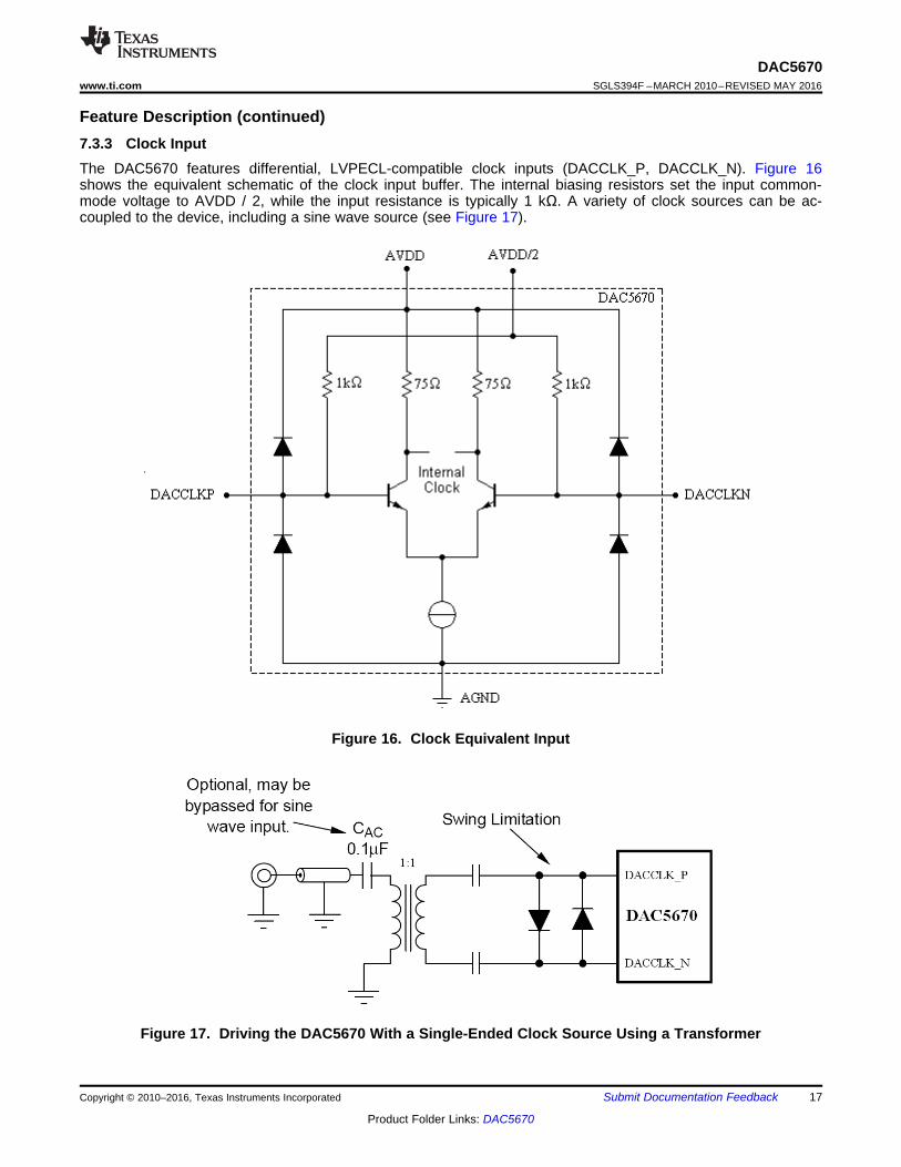
Feature Description (continued)7.3.3 Clock InputThe DAC5670 features differential, LVPECL-compatible clock inputs (DACCLK_P, DACCLK_N). Figure 16shows the equivalent schematic of the clock input buffer. The internal biasing resistors set the input common-mode voltage to AVDD / 2, while the input resistance is typically 1 kΩ. A variety of clock sources can be ac-coupled to the device, including a sine wave source (see Figure 17).
Figure 16. Clock Equivalent Input
Figure 17. Driving the DAC5670 With a Single-Ended Clock Source Using a Transformer
18
DAC5670SGLS394F –MARCH 2010–REVISED MAY 2016 www.ti.com
Product Folder Links: DAC5670
Submit Documentation Feedback Copyright © 2010–2016, Texas Instruments Incorporated
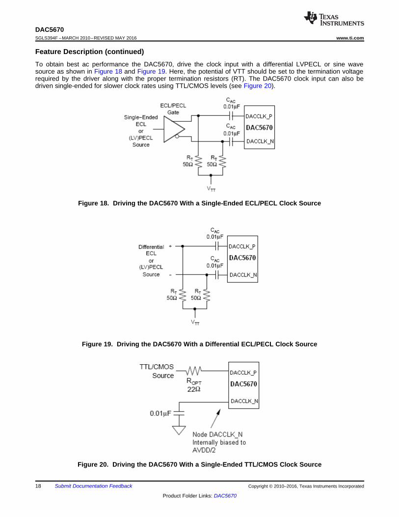
Feature Description (continued)To obtain best ac performance the DAC5670, drive the clock input with a differential LVPECL or sine wavesource as shown in Figure 18 and Figure 19. Here, the potential of VTT should be set to the termination voltagerequired by the driver along with the proper termination resistors (RT). The DAC5670 clock input can also bedriven single-ended for slower clock rates using TTL/CMOS levels (see Figure 20).
Figure 18. Driving the DAC5670 With a Single-Ended ECL/PECL Clock Source
Figure 19. Driving the DAC5670 With a Differential ECL/PECL Clock Source
Figure 20. Driving the DAC5670 With a Single-Ended TTL/CMOS Clock Source
19
DAC5670www.ti.com SGLS394F –MARCH 2010–REVISED MAY 2016
Product Folder Links: DAC5670
Submit Documentation FeedbackCopyright © 2010–2016, Texas Instruments Incorporated
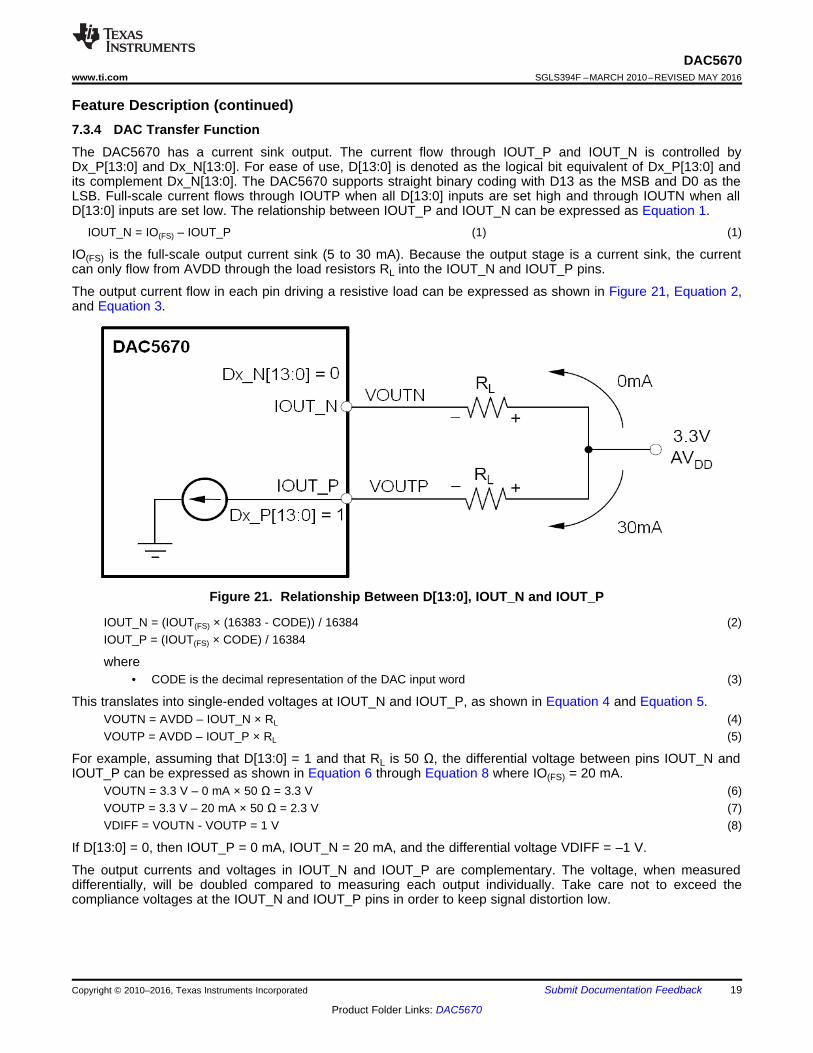
Feature Description (continued)7.3.4 DAC Transfer FunctionThe DAC5670 has a current sink output. The current flow through IOUT_P and IOUT_N is controlled byDx_P[13:0] and Dx_N[13:0]. For ease of use, D[13:0] is denoted as the logical bit equivalent of Dx_P[13:0] andits complement Dx_N[13:0]. The DAC5670 supports straight binary coding with D13 as the MSB and D0 as theLSB. Full-scale current flows through IOUTP when all D[13:0] inputs are set high and through IOUTN when allD[13:0] inputs are set low. The relationship between IOUT_P and IOUT_N can be expressed as Equation 1.
IOUT_N = IO(FS) – IOUT_P (1) (1)
IO(FS) is the full-scale output current sink (5 to 30 mA). Because the output stage is a current sink, the currentcan only flow from AVDD through the load resistors RL into the IOUT_N and IOUT_P pins.
The output current flow in each pin driving a resistive load can be expressed as shown in Figure 21, Equation 2,and Equation 3.
Figure 21. Relationship Between D[13:0], IOUT_N and IOUT_P
IOUT_N = (IOUT(FS) × (16383 - CODE)) / 16384 (2)IOUT_P = (IOUT(FS) × CODE) / 16384
where• CODE is the decimal representation of the DAC input word (3)
This translates into single-ended voltages at IOUT_N and IOUT_P, as shown in Equation 4 and Equation 5.VOUTN = AVDD – IOUT_N × RL (4)VOUTP = AVDD – IOUT_P × RL (5)
For example, assuming that D[13:0] = 1 and that RL is 50 Ω, the differential voltage between pins IOUT_N andIOUT_P can be expressed as shown in Equation 6 through Equation 8 where IO(FS) = 20 mA.
VOUTN = 3.3 V – 0 mA × 50 Ω = 3.3 V (6)VOUTP = 3.3 V – 20 mA × 50 Ω = 2.3 V (7)VDIFF = VOUTN - VOUTP = 1 V (8)
If D[13:0] = 0, then IOUT_P = 0 mA, IOUT_N = 20 mA, and the differential voltage VDIFF = –1 V.
The output currents and voltages in IOUT_N and IOUT_P are complementary. The voltage, when measureddifferentially, will be doubled compared to measuring each output individually. Take care not to exceed thecompliance voltages at the IOUT_N and IOUT_P pins in order to keep signal distortion low.
Bandgap
Reference
REFIO_IN
REFIO
RBIASOUT
RBIASIN
1.2 V Reference
External
REFIO
Filter
Capacitor
External
REFIO
Filter
Capacitor
External
RBIAS
Resistor
External
RBIAS
Resistor
+
-
20
DAC5670SGLS394F –MARCH 2010–REVISED MAY 2016 www.ti.com
Product Folder Links: DAC5670
Submit Documentation Feedback Copyright © 2010–2016, Texas Instruments Incorporated
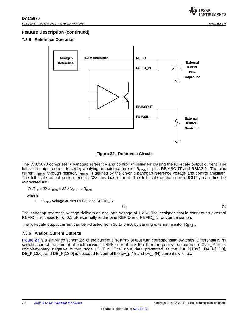
Feature Description (continued)7.3.5 Reference Operation
Figure 22. Reference Circuit
The DAC5670 comprises a bandgap reference and control amplifier for biasing the full-scale output current. Thefull-scale output current is set by applying an external resistor RBIAS to pins RBIASOUT and RBIASIN. The biascurrent, IBIAS, through resistor, RBIAS, is defined by the on-chip bandgap reference voltage and control amplifier.The full-scale output current equals 32× this bias current. The full-scale output current IOUTFS can thus beexpressed as:
IOUTFS = 32 × IBIAS = 32 × VREFIO / RBIAS
where• VREFIO voltage at pins REFIO and REFIO_IN
(9) (9)
The bandgap reference voltage delivers an accurate voltage of 1.2 V. The designer should connect an externalREFIO filter capacitor of 0.1 μF externally to the pins REFIO and REFIO_IN for compensation.
The full-scale output current can be adjusted from 30 to 5 mA by varying external resistor RBIAS .
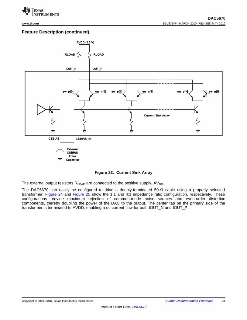
7.3.6 Analog Current OutputsFigure 23 is a simplified schematic of the current sink array output with corresponding switches. Differential NPNswitches direct the current of each individual NPN current sink to either the positive output node IOUT_P or itscomplementary negative output node IOUT_N. The input data presented at the DA_P[13:0], DA_N[13:0],DB_P[13:0], and DB_N[13:0] is decoded to control the sw_p(N) and sw_n(N) current switches.
sw_p(0) sw_n(0) sw_n(1)sw_p(1) sw_n(N)sw_p(N)
CSBIAS
External
CSBIAS
Filter
Capacitor
RLOADRLOAD
AVDD (3.3 V)
IOUT_N IOUT_P
sw_p(0) sw_n(0) sw_n(1)sw_p(1) sw_n(N)sw_p(N)
CSBIAS_INCSBIAS
External
CSBIAS
Filter
Capacitor
Current Sink Array
21
DAC5670www.ti.com SGLS394F –MARCH 2010–REVISED MAY 2016
Product Folder Links: DAC5670
Submit Documentation FeedbackCopyright © 2010–2016, Texas Instruments Incorporated
Feature Description (continued)
Figure 23. Current Sink Array
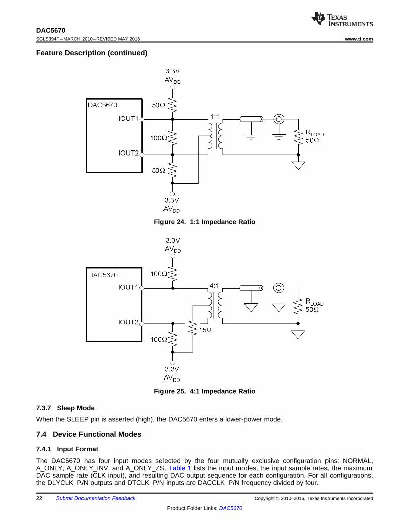
The external output resistors RLOAD are connected to the positive supply, AVDD.
The DAC5670 can easily be configured to drive a doubly-terminated 50-Ω cable using a properly selectedtransformer. Figure 24 and Figure 25 show the 1:1 and 4:1 impedance ratio configuration, respectively. Theseconfigurations provide maximum rejection of common-mode noise sources and even-order distortioncomponents, thereby doubling the power of the DAC to the output. The center tap on the primary side of thetransformer is terminated to AVDD, enabling a dc current flow for both IOUT_N and IOUT_P.
22
DAC5670SGLS394F –MARCH 2010–REVISED MAY 2016 www.ti.com
Product Folder Links: DAC5670
Submit Documentation Feedback Copyright © 2010–2016, Texas Instruments Incorporated
Feature Description (continued)
Figure 24. 1:1 Impedance Ratio
Figure 25. 4:1 Impedance Ratio
7.3.7 Sleep ModeWhen the SLEEP pin is asserted (high), the DAC5670 enters a lower-power mode.
7.4 Device Functional Modes
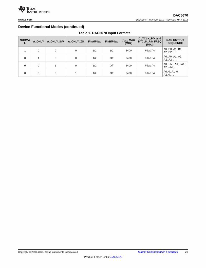
7.4.1 Input FormatThe DAC5670 has four input modes selected by the four mutually exclusive configuration pins: NORMAL,A_ONLY, A_ONLY_INV, and A_ONLY_ZS. Table 1 lists the input modes, the input sample rates, the maximumDAC sample rate (CLK input), and resulting DAC output sequence for each configuration. For all configurations,the DLYCLK_P/N outputs and DTCLK_P/N inputs are DACCLK_P/N frequency divided by four.
23
DAC5670www.ti.com SGLS394F –MARCH 2010–REVISED MAY 2016
Product Folder Links: DAC5670
Submit Documentation FeedbackCopyright © 2010–2016, Texas Instruments Incorporated
Device Functional Modes (continued)Table 1. DAC5670 Input Formats
NORMAL A_ONLY A_ONLY_INV A_ONLY_ZS FinA/Fdac FinB/Fdac ƒDAC MAX
(MHz)DLYCLK_P/N andDTCLK_P/N FREQ
(MHz)DAC OUTPUTSEQUENCE
1 0 0 0 1/2 1/2 2400 Fdac / 4 A0, B0, A1, B1,A2, B2, . . .
0 1 0 0 1/2 Off 2400 Fdac / 4 A0, A0, A1, A1,A2, A2, . . .
0 0 1 0 1/2 Off 2400 Fdac / 4 A0, –A0, A1, –A1,A2, –A2, . .
0 0 0 1 1/2 Off 2400 Fdac / 4 A0, 0, A1, 0,A2, 0, . . .
SLEEP
InputRegisters
DA_P[13:0]
DA_N[13:0]
DB_P[13:0]
DB_N[13:0]
DTCLK_P
NO
RM
AL
DTCLK_N
RESTART
INV_CLK
DLYCLK_P
DLYCLK_N
A_O
NLY
A_O
NLY
_IN
V
A_O
NLY
_Z
SMode Controls
1:1
3.3 V(AV )DD
3.3 V(AV )DD
3.3 V(AV )DD
50 Ω
100 Ω
IOUT
IOUT
0.01 Fµ
Output
R
50LOAD
ΩX
CSCAP
CSCAP_IN
RBIASOUT
RBIAS
Rbias
REFIO_IN
REFIO
Demuxand
Format
14 bit2.4GspsDAC
BandgapRef 0.001 Fµ
X
CLKIN
50 Ω
100 pF
100 pF DA
CC
LK
_P
DA
CC
LK
_N
LV
DS
_H
TB
÷2 ÷2
PhaseDetector
LoopFilter
VariableDelay
100
100
100
24
DAC5670SGLS394F –MARCH 2010–REVISED MAY 2016 www.ti.com
Product Folder Links: DAC5670
Submit Documentation Feedback Copyright © 2010–2016, Texas Instruments Incorporated
8 Application and Implementation
NOTEInformation in the following applications sections is not part of the TI componentspecification, and TI does not warrant its accuracy or completeness. TI’s customers areresponsible for determining suitability of components for their purposes. Customers shouldvalidate and test their design implementation to confirm system functionality.
8.1 Application InformationThe DAC5670 is a 14-bit DAC with max input rate of 2.4 GSPS. The DAC5670 is also suitable to operate atlower sample rates without the use of the DLL for input interface timing.
8.2 Typical Application
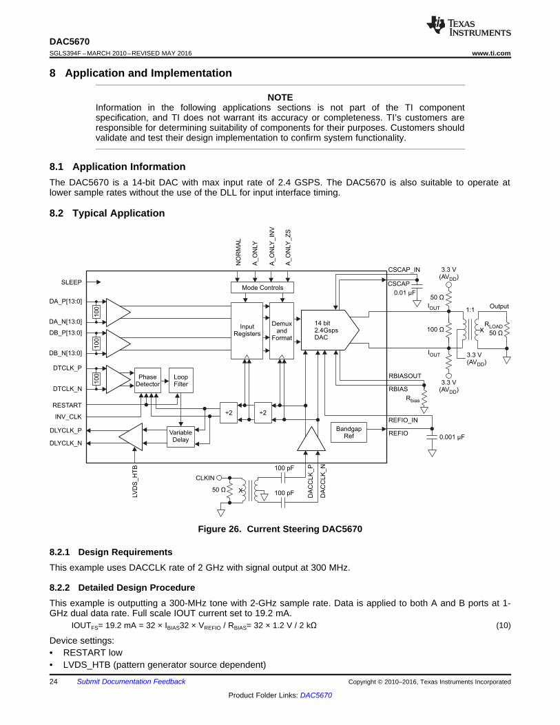
Figure 26. Current Steering DAC5670
8.2.1 Design RequirementsThis example uses DACCLK rate of 2 GHz with signal output at 300 MHz.
8.2.2 Detailed Design ProcedureThis example is outputting a 300-MHz tone with 2-GHz sample rate. Data is applied to both A and B ports at 1-GHz dual data rate. Full scale IOUT current set to 19.2 mA.
IOUTFS= 19.2 mA = 32 × IBIAS32 × VREFIO / RBIAS= 32 × 1.2 V / 2 kΩ (10)
Device settings:• RESTART low• LVDS_HTB (pattern generator source dependent)
Frequency
Pow
er (
dBm
)
0 1E+8 2E+8 3E+8 4E+8 5E+8 6E+8 7E+8 8E+8 9E+8-18
-16
-14
-12
-10
-8
-6
-4
-2
0
2
D002
Power (dBm)sinx/x (dBm)Corrected
25
DAC5670www.ti.com SGLS394F –MARCH 2010–REVISED MAY 2016
Product Folder Links: DAC5670
Submit Documentation FeedbackCopyright © 2010–2016, Texas Instruments Incorporated
Typical Application (continued)• INV_CLK as necessary for DLL lock• SLEEP low• NORMAL high• A_ONLY low• A_ONLY_INV low• A_ONLY_ZS low• DA_P[0:13], DA_N[0:13], DB_P[0:13],DB_N[0:13] sourced from pattern generator generating 300-MHz tone
with 65536 sample depth• RBIAS 2 kΩ to GND
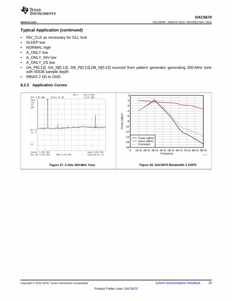
8.2.3 Application Curves
Figure 27. 2-GHz 300-MHz Tone Figure 28. DAC5670 Bandwidth 2 GSPS
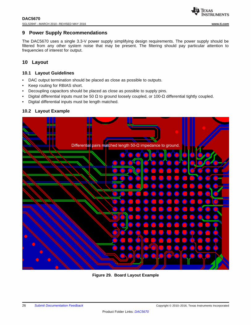
Differential pairs matched length 50- impedance to ground.Ω
26
DAC5670SGLS394F –MARCH 2010–REVISED MAY 2016 www.ti.com
Product Folder Links: DAC5670
Submit Documentation Feedback Copyright © 2010–2016, Texas Instruments Incorporated
9 Power Supply RecommendationsThe DAC5670 uses a single 3.3-V power supply simplifying design requirements. The power supply should befiltered from any other system noise that may be present. The filtering should pay particular attention tofrequencies of interest for output.
10 Layout
10.1 Layout Guidelines• DAC output termination should be placed as close as possible to outputs.• Keep routing for RBIAS short.• Decoupling capacitors should be placed as close as possible to supply pins.• Digital differential inputs must be 50 Ω to ground loosely coupled, or 100-Ω differential tightly coupled.• Digital differential inputs must be length matched.
10.2 Layout Example
Figure 29. Board Layout Example
27
DAC5670www.ti.com SGLS394F –MARCH 2010–REVISED MAY 2016
Product Folder Links: DAC5670
Submit Documentation FeedbackCopyright © 2010–2016, Texas Instruments Incorporated
11 Device and Documentation Support
11.1 Device Support
11.1.1 Device Nomenclature
11.1.1.1 Definitions of Specifications and TerminologyDifferential Nonlinearity (DNL) Defined as the variation in analog output associated with an ideal 1 LSB change
in the digital input code.
Gain Drift Defined as the maximum change in gain, in terms of ppm of full-scale range (FSR) per °C, from thevalue at 25°C to values over the full operating temperature range.
Gain Error Defined as the percentage error in the ratio between the measured full-scale output current and thevalue of the ideal full-scale output (32 x VREFIO / RBIAS). A VREFIO of 1.2 V is used to measure thegain error with an external reference voltage applied. With an internal reference, this error includesthe deviation of VREFIO (internal bandgap reference voltage) from the typical value of 1.2 V.
Integral Nonlinearity (INL) Defined as the maximum deviation of the actual analog output from the ideal output,determined by a straight line drawn from zero scale to full scale.
Intermodulation Distortion (IMD3, IMD) The two-tone IMD3 or four-tone IMD is defined as the ratio (in dBc) ofthe worst third-order (or higher) intermodulation distortion product to either fundamental output tone.
Offset Drift Defined as the maximum change in dc offset, in terms of ppm of full-scale range (FSR) per °C, fromthe value at 25°C to values over the full operating temperature range.
Offset Error Defined as the percentage error in the ratio of the differential output current (IOUT_P – IOUT_N) tohalf of the full-scale output current for input code 8192.
Output Compliance Range Defined as the minimum and maximum allowable voltage at the output of thecurrent-output DAC. Exceeding this limit may result in reduced reliability of the device or adverselyaffect distortion performance.
Power Supply Rejection Ratio (PSRR) Defined as the percentage error in the ratio of the delta IOUT and deltasupply voltage normalized with respect to the ideal IOUT current.
Reference Voltage Drift Defined as the maximum change of the reference voltage in ppm per °C from value atambient (25°C) to values over the full operating temperature range.
Signal-to-Noise Ratio (SNR) Defined as the ratio of the RMS value of the fundamental output signal to the RMSsum of all other spectral components below the Nyquist frequency, including noise, but excludingthe first six harmonics and dc.
Spurious Free Dynamic Range (SFDR) Defined as the difference (in dBc) between the peak amplitude of theoutput signal and the peak spurious signal.
Total Harmonic Distortion (THD) Defined as the ratio of the RMS sum of the first six harmonic components tothe RMS value of the fundamental output signal.
11.2 Community ResourcesThe following links connect to TI community resources. Linked contents are provided "AS IS" by the respectivecontributors. They do not constitute TI specifications and do not necessarily reflect TI's views; see TI's Terms ofUse.
TI E2E™ Online Community TI's Engineer-to-Engineer (E2E) Community. Created to foster collaborationamong engineers. At e2e.ti.com, you can ask questions, share knowledge, explore ideas and helpsolve problems with fellow engineers.
Design Support TI's Design Support Quickly find helpful E2E forums along with design support tools andcontact information for technical support.
11.3 TrademarksE2E is a trademark of Texas Instruments.
28
DAC5670SGLS394F –MARCH 2010–REVISED MAY 2016 www.ti.com
Product Folder Links: DAC5670
Submit Documentation Feedback Copyright © 2010–2016, Texas Instruments Incorporated
11.3 Trademarks (continued)HyperTransport is a trademark of HyperTransport Technology Consortium.All other trademarks are the property of their respective owners.
11.4 Electrostatic Discharge CautionThese devices have limited built-in ESD protection. The leads should be shorted together or the device placed in conductive foamduring storage or handling to prevent electrostatic damage to the MOS gates.
11.5 GlossarySLYZ022 — TI Glossary.
This glossary lists and explains terms, acronyms, and definitions.
12 Mechanical, Packaging, and Orderable InformationThe following pages include mechanical, packaging, and orderable information. This information is the mostcurrent data available for the designated devices. This data is subject to change without notice and revision ofthis document. For browser-based versions of this data sheet, refer to the left-hand navigation.
PACKAGE OPTION ADDENDUM
www.ti.com 22-Jun-2018
Addendum-Page 1
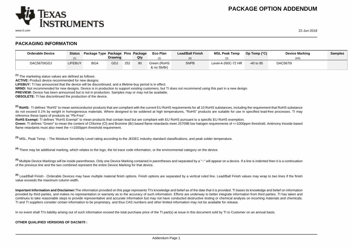
PACKAGING INFORMATION
Orderable Device Status(1)
Package Type PackageDrawing
Pins PackageQty
Eco Plan(2)
Lead/Ball Finish(6)
MSL Peak Temp(3)
Op Temp (°C) Device Marking(4/5)
Samples
DAC5670IGDJ LIFEBUY BGA GDJ 252 90 Green (RoHS& no Sb/Br)
SNPB Level-4-260C-72 HR -40 to 85 DAC5670I
(1) The marketing status values are defined as follows:ACTIVE: Product device recommended for new designs.LIFEBUY: TI has announced that the device will be discontinued, and a lifetime-buy period is in effect.NRND: Not recommended for new designs. Device is in production to support existing customers, but TI does not recommend using this part in a new design.PREVIEW: Device has been announced but is not in production. Samples may or may not be available.OBSOLETE: TI has discontinued the production of the device.
(2) RoHS: TI defines "RoHS" to mean semiconductor products that are compliant with the current EU RoHS requirements for all 10 RoHS substances, including the requirement that RoHS substancedo not exceed 0.1% by weight in homogeneous materials. Where designed to be soldered at high temperatures, "RoHS" products are suitable for use in specified lead-free processes. TI mayreference these types of products as "Pb-Free".RoHS Exempt: TI defines "RoHS Exempt" to mean products that contain lead but are compliant with EU RoHS pursuant to a specific EU RoHS exemption.Green: TI defines "Green" to mean the content of Chlorine (Cl) and Bromine (Br) based flame retardants meet JS709B low halogen requirements of <=1000ppm threshold. Antimony trioxide basedflame retardants must also meet the <=1000ppm threshold requirement.
(3) MSL, Peak Temp. - The Moisture Sensitivity Level rating according to the JEDEC industry standard classifications, and peak solder temperature.
(4) There may be additional marking, which relates to the logo, the lot trace code information, or the environmental category on the device.
(5) Multiple Device Markings will be inside parentheses. Only one Device Marking contained in parentheses and separated by a "~" will appear on a device. If a line is indented then it is a continuationof the previous line and the two combined represent the entire Device Marking for that device.
(6) Lead/Ball Finish - Orderable Devices may have multiple material finish options. Finish options are separated by a vertical ruled line. Lead/Ball Finish values may wrap to two lines if the finishvalue exceeds the maximum column width.
Important Information and Disclaimer:The information provided on this page represents TI's knowledge and belief as of the date that it is provided. TI bases its knowledge and belief on informationprovided by third parties, and makes no representation or warranty as to the accuracy of such information. Efforts are underway to better integrate information from third parties. TI has taken andcontinues to take reasonable steps to provide representative and accurate information but may not have conducted destructive testing or chemical analysis on incoming materials and chemicals.TI and TI suppliers consider certain information to be proprietary, and thus CAS numbers and other limited information may not be available for release.
In no event shall TI's liability arising out of such information exceed the total purchase price of the TI part(s) at issue in this document sold by TI to Customer on an annual basis.
OTHER QUALIFIED VERSIONS OF DAC5670 :
PACKAGE OPTION ADDENDUM
www.ti.com 22-Jun-2018
Addendum-Page 2
• Space: DAC5670-SP
NOTE: Qualified Version Definitions:
• Space - Radiation tolerant, ceramic packaging and qualified for use in Space-based application
IMPORTANT NOTICE
Texas Instruments Incorporated (TI) reserves the right to make corrections, enhancements, improvements and other changes to itssemiconductor products and services per JESD46, latest issue, and to discontinue any product or service per JESD48, latest issue. Buyersshould obtain the latest relevant information before placing orders and should verify that such information is current and complete.TI’s published terms of sale for semiconductor products (http://www.ti.com/sc/docs/stdterms.htm) apply to the sale of packaged integratedcircuit products that TI has qualified and released to market. Additional terms may apply to the use or sale of other types of TI products andservices.Reproduction of significant portions of TI information in TI data sheets is permissible only if reproduction is without alteration and isaccompanied by all associated warranties, conditions, limitations, and notices. TI is not responsible or liable for such reproduceddocumentation. Information of third parties may be subject to additional restrictions. Resale of TI products or services with statementsdifferent from or beyond the parameters stated by TI for that product or service voids all express and any implied warranties for theassociated TI product or service and is an unfair and deceptive business practice. TI is not responsible or liable for any such statements.Buyers and others who are developing systems that incorporate TI products (collectively, “Designers”) understand and agree that Designersremain responsible for using their independent analysis, evaluation and judgment in designing their applications and that Designers havefull and exclusive responsibility to assure the safety of Designers' applications and compliance of their applications (and of all TI productsused in or for Designers’ applications) with all applicable regulations, laws and other applicable requirements. Designer represents that, withrespect to their applications, Designer has all the necessary expertise to create and implement safeguards that (1) anticipate dangerousconsequences of failures, (2) monitor failures and their consequences, and (3) lessen the likelihood of failures that might cause harm andtake appropriate actions. Designer agrees that prior to using or distributing any applications that include TI products, Designer willthoroughly test such applications and the functionality of such TI products as used in such applications.TI’s provision of technical, application or other design advice, quality characterization, reliability data or other services or information,including, but not limited to, reference designs and materials relating to evaluation modules, (collectively, “TI Resources”) are intended toassist designers who are developing applications that incorporate TI products; by downloading, accessing or using TI Resources in anyway, Designer (individually or, if Designer is acting on behalf of a company, Designer’s company) agrees to use any particular TI Resourcesolely for this purpose and subject to the terms of this Notice.TI’s provision of TI Resources does not expand or otherwise alter TI’s applicable published warranties or warranty disclaimers for TIproducts, and no additional obligations or liabilities arise from TI providing such TI Resources. TI reserves the right to make corrections,enhancements, improvements and other changes to its TI Resources. TI has not conducted any testing other than that specificallydescribed in the published documentation for a particular TI Resource.Designer is authorized to use, copy and modify any individual TI Resource only in connection with the development of applications thatinclude the TI product(s) identified in such TI Resource. NO OTHER LICENSE, EXPRESS OR IMPLIED, BY ESTOPPEL OR OTHERWISETO ANY OTHER TI INTELLECTUAL PROPERTY RIGHT, AND NO LICENSE TO ANY TECHNOLOGY OR INTELLECTUAL PROPERTYRIGHT OF TI OR ANY THIRD PARTY IS GRANTED HEREIN, including but not limited to any patent right, copyright, mask work right, orother intellectual property right relating to any combination, machine, or process in which TI products or services are used. Informationregarding or referencing third-party products or services does not constitute a license to use such products or services, or a warranty orendorsement thereof. Use of TI Resources may require a license from a third party under the patents or other intellectual property of thethird party, or a license from TI under the patents or other intellectual property of TI.TI RESOURCES ARE PROVIDED “AS IS” AND WITH ALL FAULTS. TI DISCLAIMS ALL OTHER WARRANTIES ORREPRESENTATIONS, EXPRESS OR IMPLIED, REGARDING RESOURCES OR USE THEREOF, INCLUDING BUT NOT LIMITED TOACCURACY OR COMPLETENESS, TITLE, ANY EPIDEMIC FAILURE WARRANTY AND ANY IMPLIED WARRANTIES OFMERCHANTABILITY, FITNESS FOR A PARTICULAR PURPOSE, AND NON-INFRINGEMENT OF ANY THIRD PARTY INTELLECTUALPROPERTY RIGHTS. TI SHALL NOT BE LIABLE FOR AND SHALL NOT DEFEND OR INDEMNIFY DESIGNER AGAINST ANY CLAIM,INCLUDING BUT NOT LIMITED TO ANY INFRINGEMENT CLAIM THAT RELATES TO OR IS BASED ON ANY COMBINATION OFPRODUCTS EVEN IF DESCRIBED IN TI RESOURCES OR OTHERWISE. IN NO EVENT SHALL TI BE LIABLE FOR ANY ACTUAL,DIRECT, SPECIAL, COLLATERAL, INDIRECT, PUNITIVE, INCIDENTAL, CONSEQUENTIAL OR EXEMPLARY DAMAGES INCONNECTION WITH OR ARISING OUT OF TI RESOURCES OR USE THEREOF, AND REGARDLESS OF WHETHER TI HAS BEENADVISED OF THE POSSIBILITY OF SUCH DAMAGES.Unless TI has explicitly designated an individual product as meeting the requirements of a particular industry standard (e.g., ISO/TS 16949and ISO 26262), TI is not responsible for any failure to meet such industry standard requirements.Where TI specifically promotes products as facilitating functional safety or as compliant with industry functional safety standards, suchproducts are intended to help enable customers to design and create their own applications that meet applicable functional safety standardsand requirements. Using products in an application does not by itself establish any safety features in the application. Designers mustensure compliance with safety-related requirements and standards applicable to their applications. Designer may not use any TI products inlife-critical medical equipment unless authorized officers of the parties have executed a special contract specifically governing such use.Life-critical medical equipment is medical equipment where failure of such equipment would cause serious bodily injury or death (e.g., lifesupport, pacemakers, defibrillators, heart pumps, neurostimulators, and implantables). Such equipment includes, without limitation, allmedical devices identified by the U.S. Food and Drug Administration as Class III devices and equivalent classifications outside the U.S.TI may expressly designate certain products as completing a particular qualification (e.g., Q100, Military Grade, or Enhanced Product).Designers agree that it has the necessary expertise to select the product with the appropriate qualification designation for their applicationsand that proper product selection is at Designers’ own risk. Designers are solely responsible for compliance with all legal and regulatoryrequirements in connection with such selection.Designer will fully indemnify TI and its representatives against any damages, costs, losses, and/or liabilities arising out of Designer’s non-compliance with the terms and provisions of this Notice.
Mailing Address: Texas Instruments, Post Office Box 655303, Dallas, Texas 75265Copyright © 2018, Texas Instruments Incorporated


![DAC5670-SP 14-Bit 2.4-GSPS Digital-to-Analog … · DAC5670-SP SGLS386F –JANUARY 2009–REVISED OCTOBER 2014 Pin Functions (continued) PIN TYPE DESCRIPTION NAME NO. DA_P[13] J13](https://img.pdfslide.net/doc/110x75/5b8dd93e09d3f228638ca7a3/dac5670-sp-14-bit-24-gsps-digital-to-analog-dac5670-sp-sgls386f-january.jpg)