Embed Size (px)
Citation preview
DATA SHEET
Product specificationSupersedes data of 1998 May 12File under Integrated Circuits, IC02
1999 Jul 13
INTEGRATED CIRCUITS
TDA4853; TDA4854I2C-bus autosync deflectioncontrollers for PC/TV monitors
1999 Jul 13 2
Philips Semiconductors Product specification
I2C-bus autosync deflection controllers forPC/TV monitors
TDA4853; TDA4854
FEATURES
Concept features
• Full horizontal plus vertical autosync capability; TV andVCR mode included
• Extended horizontal frequency range from15 to 130 kHz
• Comprehensive set of I2C-bus driven geometryadjustments and functions, including standby mode
• Very good vertical linearity
• Moire cancellation
• Start-up and switch-off sequence for safe operation ofall power components
• X-ray protection
• Flexible switched mode B+ supply function block forfeedback and feed forward converter
• Internally stabilized voltage reference
• Drive signal for focus amplifiers with combinedhorizontal and vertical parabola waveforms (TDA4854)
• DC controllable inputs for Extremely High Tension(EHT) compensation
• SDIP32 package.
Synchronization
• Can handle all sync signals (horizontal, vertical,composite and sync-on-video)
• Output for video clamping (leading/trailing edgeselectable by I2C-bus), vertical blanking and protectionblanking
• Output for fast unlock status of horizontalsynchronization and blanking on grid 1 of picture tube.
Horizontal section
• I2C-bus controllable wide range linear picture position,pin unbalance and parallelogram correction viahorizontal phase
• Frequency-locked loop for smooth catching of horizontalfrequency
• TV mode at 15.625 or 15.750 kHz selectable by I2C-bus
• Simple frequency preset of fmin and fmax by externalresistors
• Low jitter
• Soft start for horizontal and B+ control drive signals.
Vertical section
• I2C-bus controllable vertical picture size, pictureposition, linearity (S-correction) and linearity balance
• Output for I2C-bus controllable vertical sawtooth andparabola (for pin unbalance and parallelogram)
• Vertical picture size independent of frequency
• Differential current outputs for DC coupling to verticalbooster
• 50 to 160 Hz vertical autosync range.
East-West (EW) section
• I2C-bus controllable output for horizontal pincushion,horizontal size, corner and trapezium correction
• Optional tracking of EW drive waveform with linefrequency selectable by I2C-bus.
Focus section of TDA4854
• I2C-bus controllable output for horizontal and verticalparabolas
• Vertical parabola is independent of frequency and trackswith vertical adjustments
• Horizontal parabola independent of frequency
• Pre-correction of delay in focus output stage.
1999 Jul 13 3
Philips Semiconductors Product specification
I2C-bus autosync deflection controllers forPC/TV monitors
TDA4853; TDA4854
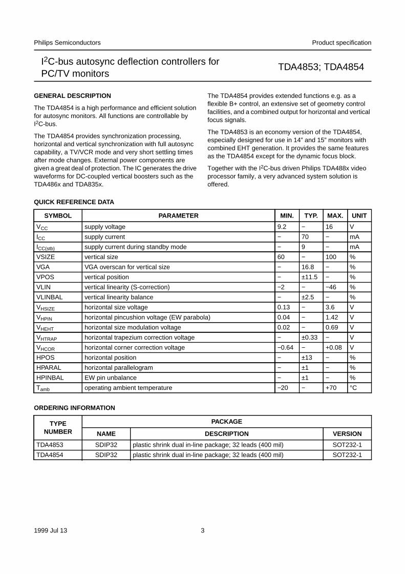
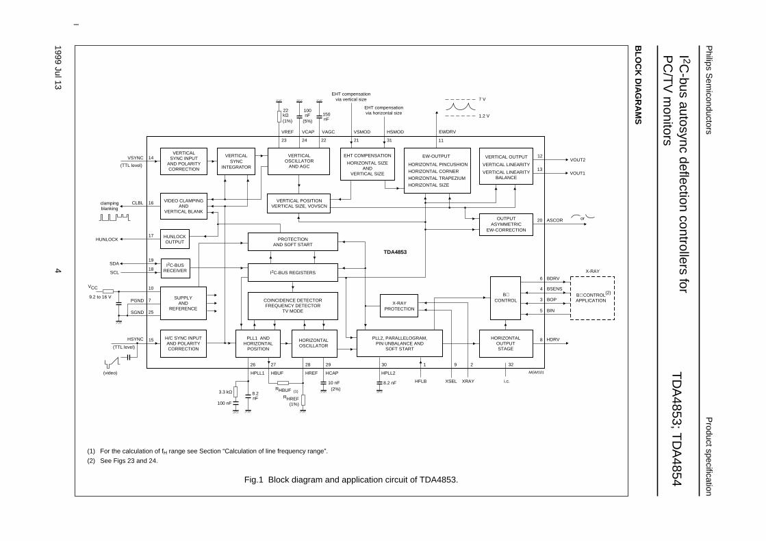
GENERAL DESCRIPTION
The TDA4854 is a high performance and efficient solutionfor autosync monitors. All functions are controllable byI2C-bus.
The TDA4854 provides synchronization processing,horizontal and vertical synchronization with full autosynccapability, a TV/VCR mode and very short settling timesafter mode changes. External power components aregiven a great deal of protection. The IC generates the drivewaveforms for DC-coupled vertical boosters such as theTDA486x and TDA835x.
The TDA4854 provides extended functions e.g. as aflexible B+ control, an extensive set of geometry controlfacilities, and a combined output for horizontal and verticalfocus signals.
The TDA4853 is an economy version of the TDA4854,especially designed for use in 14” and 15” monitors withcombined EHT generation. It provides the same featuresas the TDA4854 except for the dynamic focus block.
Together with the I2C-bus driven Philips TDA488x videoprocessor family, a very advanced system solution isoffered.
QUICK REFERENCE DATA
ORDERING INFORMATION
SYMBOL PARAMETER MIN. TYP. MAX. UNIT
VCC supply voltage 9.2 − 16 V
ICC supply current − 70 − mA
ICC(stb) supply current during standby mode − 9 − mA
VSIZE vertical size 60 − 100 %
VGA VGA overscan for vertical size − 16.8 − %
VPOS vertical position − ±11.5 − %
VLIN vertical linearity (S-correction) −2 − −46 %
VLINBAL vertical linearity balance − ±2.5 − %
VHSIZE horizontal size voltage 0.13 − 3.6 V
VHPIN horizontal pincushion voltage (EW parabola) 0.04 − 1.42 V
VHEHT horizontal size modulation voltage 0.02 − 0.69 V
VHTRAP horizontal trapezium correction voltage − ±0.33 − V
VHCOR horizontal corner correction voltage −0.64 − +0.08 V
HPOS horizontal position − ±13 − %
HPARAL horizontal parallelogram − ±1 − %
HPINBAL EW pin unbalance − ±1 − %
Tamb operating ambient temperature −20 − +70 °C
TYPENUMBER
PACKAGE
NAME DESCRIPTION VERSION
TDA4853 SDIP32 plastic shrink dual in-line package; 32 leads (400 mil) SOT232-1
TDA4854 SDIP32 plastic shrink dual in-line package; 32 leads (400 mil) SOT232-1
1999Jul13
4
Philips S
emiconductors
Product specification
I 2C-bus autosync deflection controllers for
PC
/TV
monitors
TD
A4853; T
DA
4854
This text is here in white to force landscape pages to be rotated correctly when browsing through the pdf in the Acrobat reader.This text is here in_white to force landscape pages to be rotated correctly when browsing through the pdf in the Acrobat reader.This text is here inThis text is here inwhite to force landscape pages to be rotated correctly when browsing through the pdf in the Acrobat reader. white to force landscape pages to be ...
BLO
CK
DIA
GR
AM
S
ook, full pagewidth
VERTICALSYNC INPUT
AND POLARITYCORRECTION
VERTICALSYNC
INTEGRATOR
VERTICALOSCILLATOR
AND AGC
EW-OUTPUT
HORIZONTAL PINCUSHION
HORIZONTAL CORNER
HORIZONTAL TRAPEZIUM
HORIZONTAL SIZE
VERTICAL LINEARITY
VERTICAL LINEARITYBALANCE
HORIZONTAL SIZE AND
VERTICAL SIZE
EHT COMPENSATION
OUTPUTASYMMETRIC
EW-CORRECTION
I2C-BUSRECEIVER
HUNLOCKOUTPUT
VERTICAL POSITIONVERTICAL SIZE, VOVSCN
VIDEO CLAMPINGAND
VERTICAL BLANK
SUPPLYAND
REFERENCE
HORIZONTALOSCILLATOR
PLL1 ANDHORIZONTAL
POSITION
PLL2, PARALLELOGRAM,PIN UNBALANCE AND
SOFT START
COINCIDENCE DETECTORFREQUENCY DETECTOR
TV MODE
I2C-BUS REGISTERS
PROTECTIONAND SOFT START
X-RAYPROTECTION
HORIZONTALOUTPUTSTAGE
B+CONTROL
22kΩ
3.3 kΩ
100 nF
8.2nF
150 nF(1%)
X-RAY
10 nFRHBUF (2%)
RHREF(1%)
(1)
B+ CONTROLAPPLICATION
(2)
(TTL level)
(TTL level)
9.2 to 16 V
i.c.
(video)
clampingblanking
14
23 22 21 31 11
100 nF
(5%)
24
VOUT212
VOUT1
ASCOR
13
BDRV
BSENS
BOP
BIN
8 HDRV
or20
17
19
18
6
4
3
5
10
7
32
25
16
15
26 27 28 29
8.2 nF
30 1
TDA4853
H/C SYNC INPUTAND POLARITYCORRECTION
MGM101
29
VERTICAL OUTPUT
SDA
SCL
HSYNC
SGND
PGND
CLBL
VSYNC
VCC
EWDRVVSMODVAGCVCAPVREF HSMOD
7 V
1.2 V
EHT compensationvia horizontal size
EHT compensationvia vertical size
HFLB
HPLL2HCAPHREFHBUFHPLL1
XRAYXSEL
HUNLOCK
Fig.1 Block diagram and application circuit of TDA4853.
(1) For the calculation of fH range see Section “Calculation of line frequency range”.
(2) See Figs 23 and 24.
1999Jul13
5
Philips S
emiconductors
Product specification
I 2C-bus autosync deflection controllers for
PC
/TV
monitors
TD
A4853; T
DA
4854
This text is here in white to force landscape pages to be rotated correctly when browsing through the pdf in the Acrobat reader.This text is here in_white to force landscape pages to be rotated correctly when browsing through the pdf in the Acrobat reader.This text is here inThis text is here inwhite to force landscape pages to be rotated correctly when browsing through the pdf in the Acrobat reader. white to force landscape pages to be ...
ook, full pagewidth
VERTICALSYNC INPUT
AND POLARITYCORRECTION
VERTICALSYNC
INTEGRATOR
VERTICALOSCILLATOR
AND AGC
EW-OUTPUT
HORIZONTAL PINCUSHION
HORIZONTAL CORNER
HORIZONTAL TRAPEZIUM
HORIZONTAL SIZE
VERTICAL LINEARITY
VERTICAL LINEARITYBALANCE
HORIZONTAL SIZE AND
VERTICAL SIZE
EHT COMPENSATION
OUTPUTASYMMETRIC
EW-CORRECTION
HORIZONTALAND VERTICAL
I2C-BUSRECEIVER
HUNLOCKOUTPUT
VERTICAL POSITIONVERTICAL SIZE, VOVSCN
VIDEO CLAMPINGAND
VERTICAL BLANK
SUPPLYAND
REFERENCE
HORIZONTALOSCILLATOR
PLL1 ANDHORIZONTAL
POSITION
PLL2, PARALLELOGRAM,PIN UNBALANCE AND
SOFT START
COINCIDENCE DETECTORFREQUENCY DETECTOR
TV MODE
I2C-BUS REGISTERS
PROTECTIONAND SOFT START
X-RAYPROTECTION
HORIZONTALOUTPUTSTAGE
B+CONTROL
22kΩ
3.3 kΩ
100 nF
8.2nF
150 nF(1%)
X-RAY
10 nFRHBUF (2%)
RHREF(1%)
(1)
B+ CONTROLAPPLICATION
(2)
(TTL level)
(TTL level)
9.2 to 16 V
(video)
clampingblanking
14
23 22 21 31 11
100 nF
(5%)
24
VOUT212
VOUT1
ASCOR
13
32 FOCUS
BDRV
BSENS
BOP
BIN
8 HDRV
or20
17
19
18
6
4
3
5
10
7
25
16
15
26 27 28 29
8.2 nF
30 1
TDA4854
H/C SYNC INPUTAND POLARITYCORRECTION
MGM065
29
VERTICAL OUTPUT
FOCUS
SDA
SCL
HSYNC
SGND
PGND
CLBL
VSYNC
VCC
EWDRVVSMODVAGCVCAPVREF HSMOD
7 V
1.2 V
EHT compensationvia horizontal size
EHT compensationvia vertical size
HFLB
HPLL2HCAPHREFHBUFHPLL1
XSEL XRAY
HUNLOCK
Fig.2 Block diagram and application circuit of TDA4854.
(1) For the calculation of fH range see Section “Calculation of line frequency range”.
(2) See Figs 23 and 24.
1999 Jul 13 6
Philips Semiconductors Product specification
I2C-bus autosync deflection controllers forPC/TV monitors
TDA4853; TDA4854
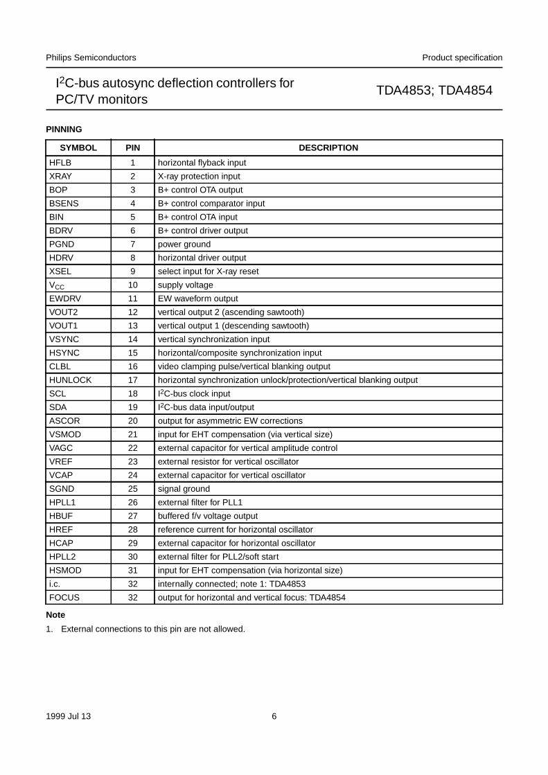
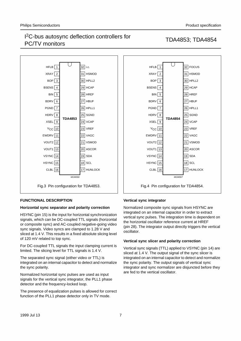
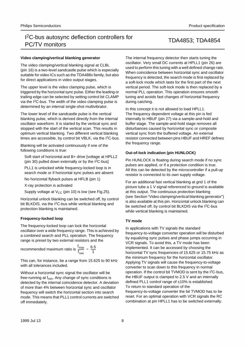
PINNING
Note
1. External connections to this pin are not allowed.
SYMBOL PIN DESCRIPTION
HFLB 1 horizontal flyback input
XRAY 2 X-ray protection input
BOP 3 B+ control OTA output
BSENS 4 B+ control comparator input
BIN 5 B+ control OTA input
BDRV 6 B+ control driver output
PGND 7 power ground
HDRV 8 horizontal driver output
XSEL 9 select input for X-ray reset
VCC 10 supply voltage
EWDRV 11 EW waveform output
VOUT2 12 vertical output 2 (ascending sawtooth)
VOUT1 13 vertical output 1 (descending sawtooth)
VSYNC 14 vertical synchronization input
HSYNC 15 horizontal/composite synchronization input
CLBL 16 video clamping pulse/vertical blanking output
HUNLOCK 17 horizontal synchronization unlock/protection/vertical blanking output
SCL 18 I2C-bus clock input
SDA 19 I2C-bus data input/output
ASCOR 20 output for asymmetric EW corrections
VSMOD 21 input for EHT compensation (via vertical size)
VAGC 22 external capacitor for vertical amplitude control
VREF 23 external resistor for vertical oscillator
VCAP 24 external capacitor for vertical oscillator
SGND 25 signal ground
HPLL1 26 external filter for PLL1
HBUF 27 buffered f/v voltage output
HREF 28 reference current for horizontal oscillator
HCAP 29 external capacitor for horizontal oscillator
HPLL2 30 external filter for PLL2/soft start
HSMOD 31 input for EHT compensation (via horizontal size)
i.c. 32 internally connected; note 1: TDA4853
FOCUS 32 output for horizontal and vertical focus: TDA4854
1999 Jul 13 7
Philips Semiconductors Product specification
I2C-bus autosync deflection controllers forPC/TV monitors
TDA4853; TDA4854
Fig.3 Pin configuration for TDA4853.
handbook, halfpage
TDA4853
MGM066
1
2
3
4
5
6
7
8
9
10
11
12
13
14
15
16
32
31
30
29
28
27
26
25
24
23
22
21
20
19
18
17
HFLB
XRAY
BOP
BSENS
BIN
BDRV
PGND
HDRV
XSEL
VCC
EWDRV
VOUT2
VOUT1
VSYNC
i.c.
HSMOD
HPLL2
HCAP
HBUF
HPLL1
HREF
SGND
VCAP
VREF
VAGC
VSMOD
ASCOR
SDA
HSYNC
CLBL
SCL
HUNLOCK
Fig.4 Pin configuration for TDA4854.
handbook, halfpage
TDA4854
MGM067
1
2
3
4
5
6
7
8
9
10
11
12
13
14
15
16
32
31
30
29
28
27
26
25
24
23
22
21
20
19
18
17
HFLB
XRAY
BOP
BSENS
BIN
BDRV
PGND
HDRV
XSEL
VCC
EWDRV
VOUT2
VOUT1
VSYNC
FOCUS
HSMOD
HPLL2
HCAP
HBUF
HPLL1
HREF
SGND
VCAP
VREF
VAGC
VSMOD
ASCOR
SDA
HSYNC
CLBL
SCL
HUNLOCK
FUNCTIONAL DESCRIPTION
Horizontal sync separator and polarity correction
HSYNC (pin 15) is the input for horizontal synchronizationsignals, which can be DC-coupled TTL signals (horizontalor composite sync) and AC-coupled negative-going videosync signals. Video syncs are clamped to 1.28 V andsliced at 1.4 V. This results in a fixed absolute slicing levelof 120 mV related to top sync.
For DC-coupled TTL signals the input clamping current islimited. The slicing level for TTL signals is 1.4 V.
The separated sync signal (either video or TTL) isintegrated on an internal capacitor to detect and normalizethe sync polarity.
Normalized horizontal sync pulses are used as inputsignals for the vertical sync integrator, the PLL1 phasedetector and the frequency-locked loop.
The presence of equalization pulses is allowed for correctfunction of the PLL1 phase detector only in TV mode.
Vertical sync integrator
Normalized composite sync signals from HSYNC areintegrated on an internal capacitor in order to extractvertical sync pulses. The integration time is dependent onthe horizontal oscillator reference current at HREF(pin 28). The integrator output directly triggers the verticaloscillator.
Vertical sync slicer and polarity correction
Vertical sync signals (TTL) applied to VSYNC (pin 14) aresliced at 1.4 V. The output signal of the sync slicer isintegrated on an internal capacitor to detect and normalizethe sync polarity. The output signals of vertical syncintegrator and sync normalizer are disjuncted before theyare fed to the vertical oscillator.
1999 Jul 13 8
Philips Semiconductors Product specification
I2C-bus autosync deflection controllers forPC/TV monitors
TDA4853; TDA4854
Video clamping/vertical blanking generator
The video clamping/vertical blanking signal at CLBL(pin 16) is a two-level sandcastle pulse which is especiallysuitable for video ICs such as the TDA488x family, but alsofor direct applications in video output stages.
The upper level is the video clamping pulse, which istriggered by the horizontal sync pulse. Either the leading ortrailing edge can be selected by setting control bit CLAMPvia the I2C-bus. The width of the video clamping pulse isdetermined by an internal single-shot multivibrator.
The lower level of the sandcastle pulse is the verticalblanking pulse, which is derived directly from the internaloscillator waveform. It is started by the vertical sync andstopped with the start of the vertical scan. This results inoptimum vertical blanking. Two different vertical blankingtimes are accessible, by control bit VBLK, via the I2C-bus.
Blanking will be activated continuously if one of thefollowing conditions is true:
Soft start of horizontal and B+ drive [voltage at HPLL2(pin 30) pulled down externally or by the I2C-bus]
PLL1 is unlocked while frequency-locked loop is insearch mode or if horizontal sync pulses are absent
No horizontal flyback pulses at HFLB (pin 1)
X-ray protection is activated
Supply voltage at VCC (pin 10) is low (see Fig.25).
Horizontal unlock blanking can be switched off, by controlbit BLKDIS, via the I2C-bus while vertical blanking andprotection blanking is maintained.
Frequency-locked loop
The frequency-locked loop can lock the horizontaloscillator over a wide frequency range. This is achieved bya combined search and PLL operation. The frequencyrange is preset by two external resistors and the
recommended maximum ratio is
This can, for instance, be a range from 15.625 to 90 kHzwith all tolerances included.
Without a horizontal sync signal the oscillator will befree-running at fmin. Any change of sync conditions isdetected by the internal coincidence detector. A deviationof more than 4% between horizontal sync and oscillatorfrequency will switch the horizontal section into searchmode. This means that PLL1 control currents are switchedoff immediately.
The internal frequency detector then starts tuning theoscillator. Very small DC currents at HPLL1 (pin 26) areused to perform this tuning with a well defined change rate.When coincidence between horizontal sync and oscillatorfrequency is detected, the search mode is first replaced bya soft-lock mode which lasts for the first part of the nextvertical period. The soft-lock mode is then replaced by anormal PLL operation. This operation ensures smoothtuning and avoids fast changes of horizontal frequencyduring catching.
In this concept it is not allowed to load HPLL1.The frequency dependent voltage at this pin is fedinternally to HBUF (pin 27) via a sample-and-hold andbuffer stage. The sample-and-hold stage removes alldisturbances caused by horizontal sync or compositevertical sync from the buffered voltage. An externalresistor connected between pins HBUF and HREF definesthe frequency range.
Out-of-lock indication (pin HUNLOCK)
Pin HUNLOCK is floating during search mode if no syncpulses are applied, or if a protection condition is true.All this can be detected by the microcontroller if a pull-upresistor is connected to its own supply voltage.
For an additional fast vertical blanking at grid 1 of thepicture tube a 1 V signal referenced to ground is availableat this output. The continuous protection blanking(see Section “Video clamping/vertical blanking generator”)is also available at this pin. Horizontal unlock blanking canbe switched off, by control bit BLKDIS via the I2C-buswhile vertical blanking is maintained.
TV mode
In applications with TV signals the standardfrequency-to-voltage converter operation will be disturbedby equalizing sync pulses and phase jumps occurring inVCR signals. To avoid this, a TV mode has beenimplemented. It can be accessed by choosing thehorizontal TV sync frequencies of 15.625 or 15.75 kHz asthe minimum frequency for the horizontal oscillator.Applying TV signals will cause the frequency-to-voltageconverter to scan down to this frequency in normaloperation. If the control bit TVMOD is sent by the I2C-bus,the HBUF output is clamped to 2.5 V and an internallydefined PLL1 control range of ±10% is established.To return to standard operation of thefrequency-to-voltage converter the bit TVMOD has to bereset. For an optimal operation with VCR signals the RCcombination at pin HPLL1 has to be switched externally.
fmax
fmin----------
6.51
--------=
1999 Jul 13 9
Philips Semiconductors Product specification
I2C-bus autosync deflection controllers forPC/TV monitors
TDA4853; TDA4854
Horizontal oscillator
The horizontal oscillator is of the relaxation type andrequires a capacitor of 10 nF to be connected at HCAP(pin 29). For optimum jitter performance the value of 10 nFmust not be changed.
The minimum oscillator frequency is determined by aresistor connected between pin HREF and ground.A resistor connected between pins HREF and HBUFdefines the frequency range.
The reference current at pin HREF also defines theintegration time constant of the vertical sync integration.
Calculation of line frequency range
The oscillator frequencies fmin and fmax must first becalculated. This is achieved by adding the spread of therelevant components to the highest and lowest syncfrequencies fsync(min) and fsync(max). The oscillator is drivenby the currents in RHREF and RHBUF.
The following example is a 31.45 to 90 kHz application:
Table 1 Calculation of total spread
Thus the typical frequency range of the oscillator in thisexample is:
The TV mode is centred around fmin with a control range of±10%. Activation of the TV mode is only allowed between15.625 and 35 kHz.
The resistors RHREF and RHBUFpar can be calculated usingthe following formulae:
The resistor RHBUFpar is calculated as the value of RHREF
and RHBUF in parallel. The formulae for RHBUF also takesinto account the voltage swing across this resistor
PLL1 phase detector
The phase detector is a standard type using switchedcurrent sources, which are independent of the horizontalfrequency. It compares the middle of the horizontal syncwith a fixed point on the oscillator sawtooth voltage.The PLL1 loop filter is connected to HPLL1 (pin 26).
See also Section “Horizontal position adjustment andcorrections”.
Horizontal position adjustment and corrections
A linear adjustment of the relative phase between thehorizontal sync and the oscillator sawtooth (in PLL1 loop)is achieved via register HPOS. Once adjusted, the relativephase remains constant over the whole frequency range.
Correction of pin unbalance and parallelogram is achievedby modulating the phase between the oscillator sawtoothand horizontal flyback (in loop PLL2) via registersHPARAL and HPINBAL. If those asymmetric EWcorrections are performed in the deflection stage, bothregisters can be disconnected from the horizontal phasevia control bit ACD. This does not change the output atpin ASCOR.
Horizontal moire cancellation
To achieve a cancellation of horizontal moire (also knownas ‘video moire’), the horizontal frequency isdivided-by-two to achieve a modulation of the horizontalphase via PLL2. The amplitude is controlled byregister HMOIRE. To avoid a visible structure on screenthe polarity changes with half of the vertical frequency.Control bit MOD disables the moire cancellation function.
spread of for f max for f min
IC ±3% ±5%
CHCAP ±2% ±2%
RHREF, RHBUF ±2% ±2%
Total ±7% ±9%
fmax fsync max( ) 1.07× 96.3 kHz= =
fmin
fsync min( )1.09
----------------------- 28.9 kHz= =
RHREF78 kHz k×× Ω
fmin 0.0012 fmin2×+ kHz[ ]
----------------------------------------------------------------- 2.61 kΩ= =
RHBUFpar78 kHz k×× Ω
fmax 0.0012 fmax2×+ kHz[ ]
-------------------------------------------------------------------- 726 Ω= =
RHBUF
RHREF RHBUFpar×RHREF RHBUFpar–---------------------------------------------- 0.8×= 805 Ω=
1999 Jul 13 10
Philips Semiconductors Product specification
I2C-bus autosync deflection controllers forPC/TV monitors
TDA4853; TDA4854
PLL2 phase detector
The PLL2 phase detector is similar to the PLL1 detectorand compares the line flyback pulse at HFLB (pin 1) withthe oscillator sawtooth voltage. The control currents areindependent of the horizontal frequency. The PLL2detector thus compensates for the delay in the externalhorizontal deflection circuit by adjusting the phase of theHDRV (pin 8) output pulse.
For the TDA4854 external modulation of the PLL2 phaseis not allowed, because this would disturb the startadvance of the horizontal focus parabola.
Soft start and standby
If HPLL2 is pulled to ground by resetting theregister SOFTST, the horizontal output pulses, verticaloutput currents and B+ control driver pulses will beinhibited. This means that HDRV (pin 8), BDRV (pin 6),VOUT1 (pin 13) and VOUT2 (pin 12) are floating in thisstate. If HPLL2 is pulled to ground by an external DCcurrent, vertical output currents stay active while HDRV(pin 8) and BDRV (pin 6) are in floating state. In both casesthe PLL2 and the frequency-locked loop are disabled,CLBL (pin 16) provides a continuous blanking signal andHUNLOCK (pin 17) is floating.
This option can be used for soft start, protection andpower-down modes. When the HPLL2 pin is releasedagain, an automatic soft start sequence on the horizontaldrive as well as on the B+ drive output will be performed(see Figs 26 and 27).
A soft start can only be performed if the supply voltage forthe IC is a minimum of 8.6 V.
The soft start timing is determined by the filter capacitor atHPLL2 (pin 30), which is charged with a constant currentduring soft start. If the voltage at pin 30 (HPLL2) reaches1.1 V, the vertical output currents are enabled. At 1.7 V thehorizontal driver stage generates very small output pulses.The width of these pulses increases with the voltage atHPLL2 until the final duty cycle is reached. The voltage atHPLL2 increases further and performs a soft start at BDRV(pin 6) as well. The voltage at HPLL2 continues to rise untilHPLL2 enters its normal operating range. The internalcharge current is now disabled. Finally PLL2 and thefrequency-locked loop are activated. If both functionsreach normal operation, HUNLOCK (pin 17) switches fromthe floating status to normal vertical blanking, andcontinuous blanking at CLBL (pin 16) is removed.
Output stage for line drive pulses [HDRV (pin 8)]
An open-collector output stage allows direct drive of aninverting driver transistor because of a low saturationvoltage of 0.3 V at 20 mA. To protect the line deflectiontransistor, the output stage is disabled (floating) for a lowsupply voltage at VCC (see Fig.25).
The duty cycle of line drive pulses is slightly dependent onthe actual horizontal frequency. This ensures optimumdrive conditions over the whole frequency range.
X-ray protection
The X-ray protection input XRAY (pin 2) provides a voltagedetector with a precise threshold. If the input voltage atXRAY exceeds this threshold for a certain time thencontrol bit SOFTST is reset, which switches the IC intoprotection mode. In this mode several pins are forced intodefined states:
HUNLOCK (pin 17) is floating
The capacitor connected to HPLL2 (pin 30) isdischarged
Horizontal output stage (HDRV) is floating
B+ control driver stage (BDRV) is floating
Vertical output stages (VOUT1 and VOUT2) are floating
CLBL provides a continuous blanking signal.
There are two different methods of restarting the IC:
1. XSEL (pin 9) is open-circuit or connected to ground.The control bit SOFTST must be set to logic 1 via theI2C-bus. The IC then returns to normal operation viasoft start.
2. XSEL (pin 9) is connected to VCC via an externalresistor. The supply voltage of the IC must be switchedoff for a certain period of time before the IC can berestarted again using the standard power-onprocedure.
1999 Jul 13 11
Philips Semiconductors Product specification
I2C-bus autosync deflection controllers forPC/TV monitors
TDA4853; TDA4854
Vertical oscillator and amplitude control
This stage is designed for fast stabilization of vertical sizeafter changes in sync frequency conditions.
The free-running frequency ffr(V) is determined by theresistor RVREF connected to pin 23 and the capacitorCVCAP connected to pin 24. The value of RVREF is not onlyoptimized for noise and linearity performance in the wholevertical and EW section, but also influences severalinternal references. Therefore the value of RVREF must notbe changed.
Capacitor CVCAP should be used to select the free-runningfrequency of the vertical oscillator in accordance with the
following formula:
To achieve a stabilized amplitude the free-runningfrequency ffr(V), without adjustment, should be at least 10%lower than the minimum trigger frequency.The contributions shown in Table 2 can be assumed.
Table 2 Calculation of ffr(V) total spread
Result for 50 to 160 Hz application:
The AGC of the vertical oscillator can be disabled bysetting control bit AGCDIS via the I2C-bus. A preciseexternal current has to be injected into VCAP (pin 24) toobtain the correct vertical size. This special applicationmode can be used when the vertical sync pulses areserrated (shifted); this condition is found in some displaymodes, e.g. when using a 100 Hz up converter for videosignals.
Application hint : VAGC (pin 22) has a high inputimpedance during scan. Therefore, the pin must not beloaded externally otherwise non-linearities in the verticaloutput currents may occur due to the changing chargecurrent during scan.
Adjustment of vertical size, VGA overscan and EHTcompensation
The amplitude of the differential output currents at VOUT1and VOUT2 can be adjusted via register VSIZE.Register VOVSCN can activate a +17% step in verticalsize for the VGA350 mode.
VSMOD (pin 21) can be used for a DC controlled EHTcompensation of vertical size by correcting the differentialoutput currents at VOUT1 and VOUT2. The EWwaveforms, (vertical focus), pin unbalance andparallelogram corrections are not affected by VSMOD.
The adjustments for vertical size and vertical position alsoaffect the waveforms of the horizontal pincushion, verticallinearity (S-correction), vertical linearity balance, focusparabola, pin unbalance and parallelogram correction.The result of this interaction is that no re-adjustment ofthese parameters is necessary after an adjustment ofvertical picture size or position.
Adjustment of vertical position, vertical linearity andvertical linearity balance
Register VPOS provides a DC shift at the sawtoothoutputs VOUT1 and VOUT2 (pins 13 and 12) and the EWdrive output EWDRV (pin 11) in such a way that the wholepicture moves vertically while maintaining the correctgeometry.
Register VLIN is used to adjust the amount of verticalS-correction in the output signal. This function can beswitched off by control bit VSC.
Register VLINBAL is used to correct the unbalance of thevertical S-correction in the output signal. This function canbe switched off by control bit VLC.
Adjustment of vertical moire cancellation
To achieve a cancellation of vertical moire (also known as‘scan moire’) the vertical picture position can be modulatedby half the vertical frequency. The amplitude of themodulation is controlled by register VMOIRE and can beswitched off via control bit MOD.
Contributing elements
Minimum frequency offset between ffr(V) andlowest trigger frequency
10%
Spread of IC ±3%
Spread of RVREF ±1%
Spread of CVCAP ±5%
Total 19%
ffr V( )1
10.8 RVREF× CVCAP×-----------------------------------------------------------=
ffr V( )50 Hz1.19
--------------- 42 Hz= =
1999 Jul 13 12
Philips Semiconductors Product specification
I2C-bus autosync deflection controllers forPC/TV monitors
TDA4853; TDA4854
Horizontal pincushion (including horizontal size,corner correction and trapezium correction)
EWDRV (pin 11) provides a complete EW drive waveform.The components horizontal pincushion, horizontal size,corner correction and trapezium correction are controlledby the registers HPIN, HSIZE, HCOR and HTRAP.HTRAP can be set to zero by control bit VPC.
The pincushion (EW parabola) amplitude, corner andtrapezium correction track with the vertical picture size(VSIZE) and also with the adjustment for vertical pictureposition (VPOS). The corner correction does not track withthe horizontal pincushion (HPIN).
Further the horizontal pincushion amplitude, corner andtrapezium correction track with the horizontal picture size,which is adjusted via register HSIZE and the analogmodulation input HSMOD.
If the DC component in the EWDRV output signal isincreased via HSIZE or IHSMOD, the pincushion, corner andtrapezium component of the EWDRV output will be
reduced by a factor of
The value 14.4 V is a virtual voltage for calculation only.The output pin can not reach this value, but the gain (andDC bias) of the external application should be such that thehorizontal deflection is reduced to zero when EWDRVreaches 14.4 V.
HSMOD can be used for a DC controlled EHTcompensation by correcting horizontal size, horizontalpincushion, corner and trapezium. The control range atthis pin tracks with the actual value of HSIZE. For anincreasing DC component VHSIZE in the EWDRV outputsignal, the DC component VHEHT caused by IHSMOD will be
reduced by a factor of as shown in the equation
above.
The whole EWDRV voltage is calculated as follows:VEWDRV = 1.2 V + [VHSIZE + VHEHT × f(HSIZE) + (VHPIN +VHCOR + VHTRAP) × g(HSIZE, HSMOD)] × h(IHREF)
Where:
Two different modes of operation can be chosen for theEW output waveform via control bit FHMULT:
1. Mode 1
Horizontal size is controlled via register HSIZE andcauses a DC shift at the EWDRV output. The completewaveform is also multiplied internally by a signalproportional to the line frequency [which is detectedvia the current at HREF (pin 28)]. This mode is to beused for driving EW diode modulator stages whichrequire a voltage proportional to the line frequency.
2. Mode 2
The EW drive waveform does not track with the linefrequency. This mode is to be used for driving EWmodulators which require a voltage independent of theline frequency.
Output stage for asymmetric correction waveforms[ASCOR (pin 20)]
This output is designed as a voltage output forsuperimposed waveforms of vertical parabola andsawtooth. The amplitude and polarity of both signals canbe changed via registers HPARAL and HPINBAL.
Application hint : The TDA4854 offers two possibilities tocontrol registers HPINBAL and HPARAL.
1. Control bit ACD = 1
The two registers now control the horizontal phase bymeans of internal modulation of the PLL2 horizontalphase control. The ASCOR output (pin 20) can be leftunused, but it will always provide an output signalbecause the ASCOR output stage is not influenced bythe control bit ACD.
2. Control bit ACD = 0
The internal modulation via PLL2 is disconnected.In order to obtain the required effect on the screen,pin ASCOR must now be fed to the DC amplifier whichcontrols the DC shift of the horizontal deflection. Thisoption is useful for applications which already use aDC shift transformer.
If the tube does not need HPINBAL and HPARAL, then pinASCOR can be used for other purposes, i.e. for a simpledynamic convergence.
1VHSIZE VHEHT 1
VHSIZE
14.4 V-----------------–
+
14.4-------------------------------------------------------------------------–
1VHSIZE
14.4 V-----------------–
VHEHT
IHSMOD
120 µA-------------------- 0.69×=
f(HSIZE) 1VHSIZE
14.4 V-----------------–=
g(HSIZE, HSMOD) 1VHSIZE VHEHT 1
VHSIZE
14.4 V-----------------–
+
14.4 V--------------------------------------------------------------------------–=
h IHREF( )IHREF
IHREFf 70kHz=
--------------------------------=
1999 Jul 13 13
Philips Semiconductors Product specification
I2C-bus autosync deflection controllers forPC/TV monitors
TDA4853; TDA4854
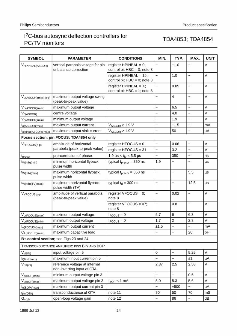
TDA4854: dynamic focus section [FOCUS (pin 32)]
This section generates a complete drive signal for dynamicfocus applications. The amplitude of the horizontalparabola is internally stabilized, thus it is independent ofthe horizontal frequency. The amplitude can be adjustedvia register HFOCUS. Changing horizontal size mayrequire a correction of HFOCUS. To compensate for thedelay in external focus amplifiers a ‘pre-correction’ for thephase of the horizontal parabola has been implemented.The amplitude of the vertical parabola is independent offrequency and tracks with all vertical adjustments.The amplitude can be adjusted via register VFOCUS.FOCUS (pin 32) is designed as a voltage output for thesuperimposed vertical and horizontal parabolas.
B+ control function block
The B+ control function block of the TDA4853; TDA4854consists of an Operational Transconductance Amplifier(OTA), a voltage comparator, a flip-flop and a dischargecircuit. This configuration allows easy applications fordifferent B+ control concepts. See also Application NoteAN96052: “B+ converter Topologies for HorizontalDeflection and EHT with TDA4855/58”.
GENERAL DESCRIPTION
The non-inverting input of the OTA is connected internallyto a high precision reference voltage. The inverting input isconnected to BIN (pin 5). An internal clamping circuit limitsthe maximum positive output voltage of the OTA.The output itself is connected to BOP (pin 3) and to theinverting input of the voltage comparator.The non-inverting input of the voltage comparator can beaccessed via BSENS (pin 4).
B+ drive pulses are generated by an internal flip-flop andfed to BDRV (pin 6) via an open-collector output stage.This flip-flop is set at the rising edge of the signal at HDRV(pin 8). The falling edge of the output signal at BDRV hasa defined delay of td(BDRV) to the rising edge of the HDRVpulse (see Fig.23). When the voltage at BSENS exceedsthe voltage at BOP, the voltage comparator output resetsthe flip-flop and, therefore, the open-collector stage atBDRV is floating again.
An internal discharge circuit allows a well defineddischarge of capacitors at BSENS. BDRV is active at aLOW-level output voltage (see Figs 23 and 24), thus itrequires an external inverting driver stage.
The B+ function block can be used for B+ deflectionmodulators in many different ways. Two popularapplication combinations are as follows:
• Boost converter in feedback mode (see Fig.23)
In this application the OTA is used as an error amplifierwith a limited output voltage range. The flip-flop is set onthe rising edge of the signal at HDRV. A reset will begenerated when the voltage at BSENS, taken from thecurrent sense resistor, exceeds the voltage at BOP.
If no reset is generated within a line period. The risingedge of the next HDRV pulse forces the flip-flop to reset.The flip-flop is set immediately after the voltage atBSENS has dropped below the threshold voltageVRESTART(BSENS).
• Buck converter in feed forward mode (see Fig.24)
This application uses an external RC combination atBSENS to provide a pulse width which is independentfrom the horizontal frequency. The capacitor is chargedvia an external resistor and discharged by the internaldischarge circuit. For normal operation the dischargecircuit is activated when the flip-flop is reset by theinternal voltage comparator. The capacitor will now bedischarged with a constant current until the internallycontrolled stop level VSTOP(BSENS) is reached. This levelwill be maintained until the rising edge of the next HDRVpulse sets the flip-flop again and disables the dischargecircuit.
If no reset is generated within a line period, the risingedge of the next HDRV pulse automatically starts thedischarge sequence and resets the flip-flop. When thevoltage at BSENS reaches the threshold voltageVRESTART(BSENS), the discharge circuit will be disabledautomatically and the flip-flop will be set immediately.This behaviour allows a definition of the maximum dutycycle of the B+ control drive pulse by the relationship ofcharge current to discharge current.
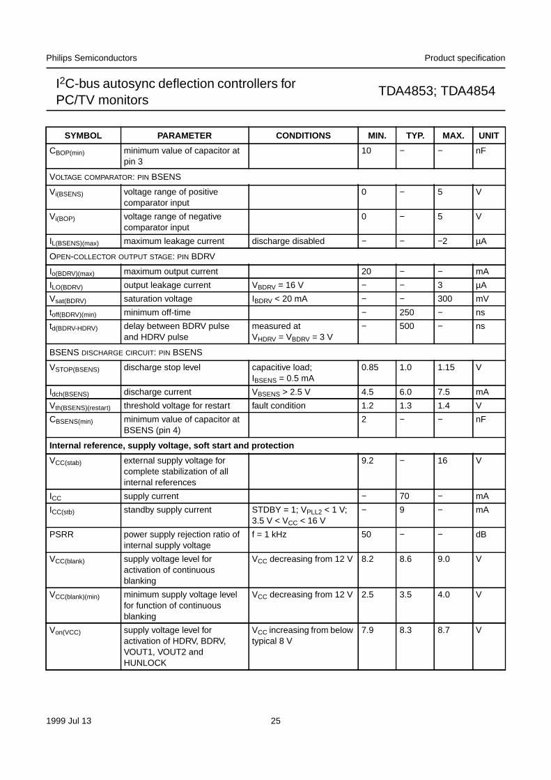
Supply voltage stabilizer, references, start-upprocedures and protection functions
The TDA4853; TDA4854 provides an internal supplyvoltage stabilizer for excellent stabilization of all internalreferences. An internal gap reference, especially designedfor low-noise, is the reference for the internal horizontaland vertical supply voltages. All internal reference currentsand drive current for the vertical output stage are derivedfrom this voltage via external resistors.
If either the supply voltage is below 8.3 V or no data fromthe I2C-bus has been received after power-up, the internalsoft start and protection functions do not allow any of thoseoutputs [HDRV, BDRV, VOUT1, VOUT2 and HUNLOCK(see Fig.25)] to be active.
1999 Jul 13 14
Philips Semiconductors Product specification
I2C-bus autosync deflection controllers forPC/TV monitors
TDA4853; TDA4854
For supply voltages below 8.3 V the internal I2C-bus willnot generate an acknowledge and the IC is in standbymode. This is because the internal protection circuit hasgenerated a reset signal for the soft startregister SOFTST. Above 8.3 V data is accepted and allregisters can be loaded. If the register SOFTST hasreceived a set from the I2C-bus, the internal soft startprocedure is released, which activates all mentionedoutputs.
If during normal operation the supply voltage has droppedbelow 8.1 V, the protection mode is activated andHUNLOCK (pin 17) changes to the protection status and isfloating. This can be detected by the microcontroller.
This protection mode has been implemented in order toprotect the deflection stages and the picture tube duringstart-up, shut-down and fault conditions. This protectionmode can be activated as shown in Table 3.
Table 3 Activation of protection mode
When the protection mode is active, several pins of theTDA4853; TDA4854 are forced into a defined state:
HDRV (horizontal driver output) is floating
BDRV (B+ control driver output) is floating
HUNLOCK (indicates, that the frequency-to-voltageconverter is out of lock) is floating (HIGH via externalpull-up resistor)
CLBL provides a continuous blanking signal
VOUT1 and VOUT2 (vertical outputs) are floating
The capacitor at HPLL2 is discharged.
If the soft start procedure is activated via the I2C-bus, all ofthese actions will be performed in a well defined sequence(see Figs 25 and 26).
ACTIVATION RESET
Low supply voltage atpin 10
increase supply voltage;reload registers;soft start via I2C-bus
Power dip, below 8.1 V reload registers;soft start via I2C-bus
X-ray protection (pin 2)triggered, XSEL (pin 9) isopen-circuit or connectedto ground
reload registers;soft start via I2C-bus
X-ray protection (pin 2)triggered, XSEL (pin 9)connected to VCC via anexternal resistor
switch VCC off and onagain, reload registers;soft start via I2C-bus
HPLL2 (pin 30) externallypulled to ground
release pin 30
1999 Jul 13 15
Philips Semiconductors Product specification
I2C-bus autosync deflection controllers forPC/TV monitors
TDA4853; TDA4854
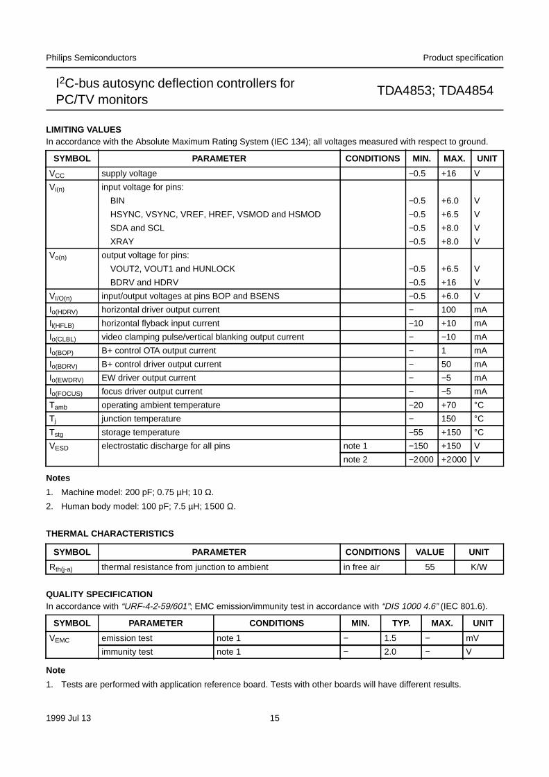
LIMITING VALUESIn accordance with the Absolute Maximum Rating System (IEC 134); all voltages measured with respect to ground.
Notes
1. Machine model: 200 pF; 0.75 µH; 10 Ω.
2. Human body model: 100 pF; 7.5 µH; 1500 Ω.
THERMAL CHARACTERISTICS
QUALITY SPECIFICATIONIn accordance with “URF-4-2-59/601”; EMC emission/immunity test in accordance with “DIS 1000 4.6” (IEC 801.6).
Note
1. Tests are performed with application reference board. Tests with other boards will have different results.
SYMBOL PARAMETER CONDITIONS MIN. MAX. UNIT
VCC supply voltage −0.5 +16 V
Vi(n) input voltage for pins:
BIN −0.5 +6.0 V
HSYNC, VSYNC, VREF, HREF, VSMOD and HSMOD −0.5 +6.5 V
SDA and SCL −0.5 +8.0 V
XRAY −0.5 +8.0 V
Vo(n) output voltage for pins:
VOUT2, VOUT1 and HUNLOCK −0.5 +6.5 V
BDRV and HDRV −0.5 +16 V
VI/O(n) input/output voltages at pins BOP and BSENS −0.5 +6.0 V
Io(HDRV) horizontal driver output current − 100 mA
Ii(HFLB) horizontal flyback input current −10 +10 mA
Io(CLBL) video clamping pulse/vertical blanking output current − −10 mA
Io(BOP) B+ control OTA output current − 1 mA
Io(BDRV) B+ control driver output current − 50 mA
Io(EWDRV) EW driver output current − −5 mA
Io(FOCUS) focus driver output current − −5 mA
Tamb operating ambient temperature −20 +70 °CTj junction temperature − 150 °CTstg storage temperature −55 +150 °CVESD electrostatic discharge for all pins note 1 −150 +150 V
note 2 −2000 +2000 V
SYMBOL PARAMETER CONDITIONS VALUE UNIT
Rth(j-a) thermal resistance from junction to ambient in free air 55 K/W
SYMBOL PARAMETER CONDITIONS MIN. TYP. MAX. UNIT
VEMC emission test note 1 − 1.5 − mV
immunity test note 1 − 2.0 − V
1999 Jul 13 16
Philips Semiconductors Product specification
I2C-bus autosync deflection controllers forPC/TV monitors
TDA4853; TDA4854
CHARACTERISTICSVCC = 12 V; Tamb = 25 °C; peripheral components in accordance with Figs 1 and 2; unless otherwise specified.
SYMBOL PARAMETER CONDITIONS MIN. TYP. MAX. UNIT
Horizontal sync separator
INPUT CHARACTERISTICS FOR DC-COUPLED TTL SIGNALS: PIN HSYNC
Vi(HSYNC) sync input signal voltage 1.7 − − V
VHSYNC(sl) slicing voltage level 1.2 1.4 1.6 V
tr(HSYNC) rise time of sync pulse 10 − 500 ns
tf(HSYNC) fall time of sync pulse 10 − 500 ns
tW(HSYNC)(min) minimum width of sync pulse 0.7 − − µs
Ii(HSYNC) input current VHSYNC = 0.8 V − − −200 µA
VHSYNC = 5.5 V − − 10 µA
INPUT CHARACTERISTICS FOR AC-COUPLED VIDEO SIGNALS (SYNC-ON-VIDEO, NEGATIVE SYNC POLARITY)
VHSYNC sync amplitude of video inputsignal voltage
Rsource = 50 Ω − 300 − mV
VHSYNC(sl) slicing voltage level(measured from top sync)
Rsource = 50 Ω 90 120 150 mV
Vclamp(HSYNC) top sync clamping voltage level Rsource = 50 Ω 1.1 1.28 1.5 V
Ich(HSYNC) charge current for couplingcapacitor
VHSYNC > Vclamp(HSYNC) 1.7 2.4 3.4 µA
tW(HSYNC)(min) minimum width of sync pulse 0.7 − − µs
Rsource(max) maximum source resistance duty cycle = 7% − − 1500 ΩRi(diff)(HSYNC) differential input resistance during sync − 80 − Ω
Automatic polarity correction for horizontal sync
horizontal sync pulse widthrelated to line period
− − 25 %
td(HPOL) delay time for changing polarity 0.3 − 1.8 ms
Vertical sync integrator
tint(V) integration time for generationof a vertical trigger pulse
fH = 15.625 kHz;IHREF = 0.52 mA
14 20 26 µs
fH = 31.45 kHz;IHREF = 1.052 mA
7 10 13 µs
fH = 64 kHz;IHREF = 2.141 mA
3.9 5.7 6.5 µs
fH = 100 kHz;IHREF = 3.345 mA
2.5 3.8 4.5 µs
Vertical sync slicer (DC-coupled, TTL compatible): pin VSYNC
Vi(VSYNC) sync input signal voltage 1.7 − − V
VVSYNC(sl) slicing voltage level 1.2 1.4 1.6 V
Ii(VSYNC) input current 0 V < VSYNC < 5.5 V − − ±10 µA
tP H( )tH
------------
1999 Jul 13 17
Philips Semiconductors Product specification
I2C-bus autosync deflection controllers forPC/TV monitors
TDA4853; TDA4854
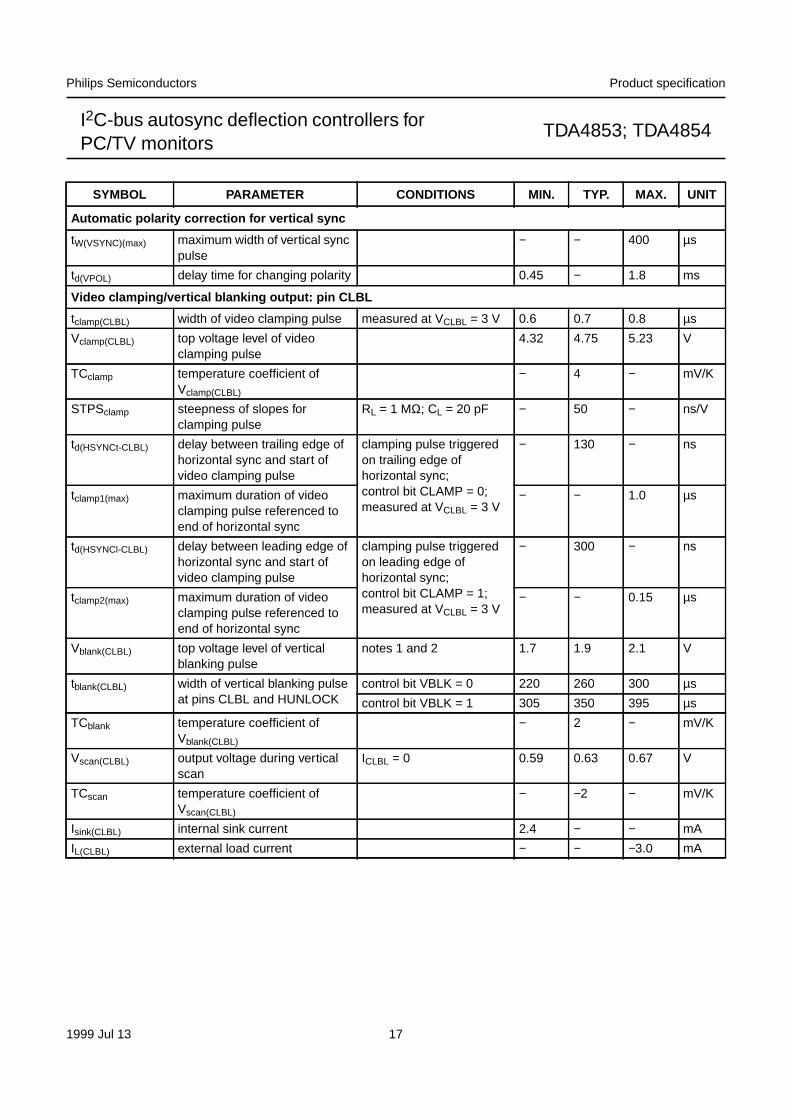
Automatic polarity correction for vertical sync
tW(VSYNC)(max) maximum width of vertical syncpulse
− − 400 µs
td(VPOL) delay time for changing polarity 0.45 − 1.8 ms
Video clamping/vertical blanking output: pin CLBL
tclamp(CLBL) width of video clamping pulse measured at VCLBL = 3 V 0.6 0.7 0.8 µs
Vclamp(CLBL) top voltage level of videoclamping pulse
4.32 4.75 5.23 V
TCclamp temperature coefficient ofVclamp(CLBL)
− 4 − mV/K
STPSclamp steepness of slopes forclamping pulse
RL = 1 MΩ; CL = 20 pF − 50 − ns/V
td(HSYNCt-CLBL) delay between trailing edge ofhorizontal sync and start ofvideo clamping pulse
clamping pulse triggeredon trailing edge ofhorizontal sync;control bit CLAMP = 0;measured at VCLBL = 3 V
− 130 − ns
tclamp1(max) maximum duration of videoclamping pulse referenced toend of horizontal sync
− − 1.0 µs
td(HSYNCl-CLBL) delay between leading edge ofhorizontal sync and start ofvideo clamping pulse
clamping pulse triggeredon leading edge ofhorizontal sync;control bit CLAMP = 1;measured at VCLBL = 3 V
− 300 − ns
tclamp2(max) maximum duration of videoclamping pulse referenced toend of horizontal sync
− − 0.15 µs
Vblank(CLBL) top voltage level of verticalblanking pulse
notes 1 and 2 1.7 1.9 2.1 V
tblank(CLBL) width of vertical blanking pulseat pins CLBL and HUNLOCK
control bit VBLK = 0 220 260 300 µs
control bit VBLK = 1 305 350 395 µs
TCblank temperature coefficient ofVblank(CLBL)
− 2 − mV/K
Vscan(CLBL) output voltage during verticalscan
ICLBL = 0 0.59 0.63 0.67 V
TCscan temperature coefficient ofVscan(CLBL)
− −2 − mV/K
Isink(CLBL) internal sink current 2.4 − − mA
IL(CLBL) external load current − − −3.0 mA
SYMBOL PARAMETER CONDITIONS MIN. TYP. MAX. UNIT
1999 Jul 13 18
Philips Semiconductors Product specification
I2C-bus autosync deflection controllers forPC/TV monitors
TDA4853; TDA4854
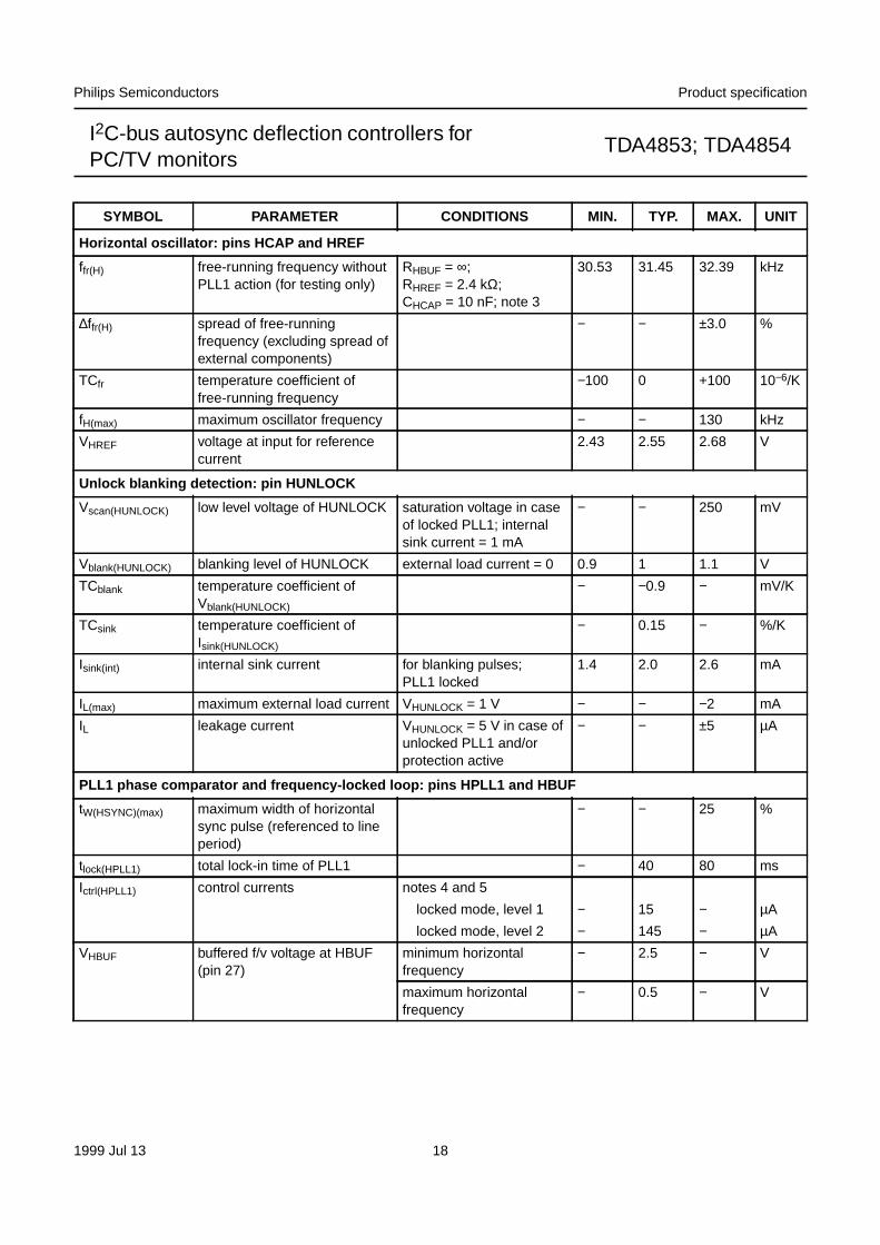
Horizontal oscillator: pins HCAP and HREF
ffr(H) free-running frequency withoutPLL1 action (for testing only)
RHBUF = ∞;RHREF = 2.4 kΩ;CHCAP = 10 nF; note 3
30.53 31.45 32.39 kHz
∆ffr(H) spread of free-runningfrequency (excluding spread ofexternal components)
− − ±3.0 %
TCfr temperature coefficient offree-running frequency
−100 0 +100 10−6/K
fH(max) maximum oscillator frequency − − 130 kHz
VHREF voltage at input for referencecurrent
2.43 2.55 2.68 V
Unlock blanking detection: pin HUNLOCK
Vscan(HUNLOCK) low level voltage of HUNLOCK saturation voltage in caseof locked PLL1; internalsink current = 1 mA
− − 250 mV
Vblank(HUNLOCK) blanking level of HUNLOCK external load current = 0 0.9 1 1.1 V
TCblank temperature coefficient ofVblank(HUNLOCK)
− −0.9 − mV/K
TCsink temperature coefficient ofIsink(HUNLOCK)
− 0.15 − %/K
Isink(int) internal sink current for blanking pulses;PLL1 locked
1.4 2.0 2.6 mA
IL(max) maximum external load current VHUNLOCK = 1 V − − −2 mA
IL leakage current VHUNLOCK = 5 V in case ofunlocked PLL1 and/orprotection active
− − ±5 µA
PLL1 phase comparator and frequency-locked loop: pins HPLL1 and HBUF
tW(HSYNC)(max) maximum width of horizontalsync pulse (referenced to lineperiod)
− − 25 %
tlock(HPLL1) total lock-in time of PLL1 − 40 80 ms
Ictrl(HPLL1) control currents notes 4 and 5
locked mode, level 1 − 15 − µA
locked mode, level 2 − 145 − µA
VHBUF buffered f/v voltage at HBUF(pin 27)
minimum horizontalfrequency
− 2.5 − V
maximum horizontalfrequency
− 0.5 − V
SYMBOL PARAMETER CONDITIONS MIN. TYP. MAX. UNIT
1999 Jul 13 19
Philips Semiconductors Product specification
I2C-bus autosync deflection controllers forPC/TV monitors
TDA4853; TDA4854
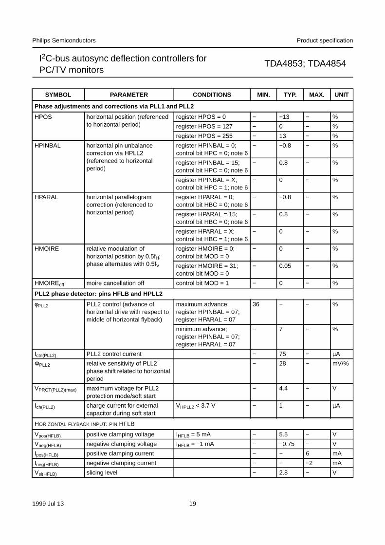
Phase adjustments and corrections via PLL1 and PLL2
HPOS horizontal position (referencedto horizontal period)
register HPOS = 0 − −13 − %
register HPOS = 127 − 0 − %
register HPOS = 255 − 13 − %
HPINBAL horizontal pin unbalancecorrection via HPLL2(referenced to horizontalperiod)
register HPINBAL = 0;control bit HPC = 0; note 6
− −0.8 − %
register HPINBAL = 15;control bit HPC = 0; note 6
− 0.8 − %
register HPINBAL = X;control bit HPC = 1; note 6
− 0 − %
HPARAL horizontal parallelogramcorrection (referenced tohorizontal period)
register HPARAL = 0;control bit HBC = 0; note 6
− −0.8 − %
register HPARAL = 15;control bit HBC = 0; note 6
− 0.8 − %
register HPARAL = X;control bit HBC = 1; note 6
− 0 − %
HMOIRE relative modulation ofhorizontal position by 0.5fH;phase alternates with 0.5fV
register HMOIRE = 0;control bit MOD = 0
− 0 − %
register HMOIRE = 31;control bit MOD = 0
− 0.05 − %
HMOIREoff moire cancellation off control bit MOD = 1 − 0 − %
PLL2 phase detector: pins HFLB and HPLL2
φPLL2 PLL2 control (advance ofhorizontal drive with respect tomiddle of horizontal flyback)
maximum advance;register HPINBAL = 07;register HPARAL = 07
36 − − %
minimum advance;register HPINBAL = 07;register HPARAL = 07
− 7 − %
Ictrl(PLL2) PLL2 control current − 75 − µA
ΦPLL2 relative sensitivity of PLL2phase shift related to horizontalperiod
− 28 − mV/%
VPROT(PLL2)(max) maximum voltage for PLL2protection mode/soft start
− 4.4 − V
Ich(PLL2) charge current for externalcapacitor during soft start
VHPLL2 < 3.7 V − 1 − µA
HORIZONTAL FLYBACK INPUT: PIN HFLB
Vpos(HFLB) positive clamping voltage IHFLB = 5 mA − 5.5 − V
Vneg(HFLB) negative clamping voltage IHFLB = −1 mA − −0.75 − V
Ipos(HFLB) positive clamping current − − 6 mA
Ineg(HFLB) negative clamping current − − −2 mA
Vsl(HFLB) slicing level − 2.8 − V
SYMBOL PARAMETER CONDITIONS MIN. TYP. MAX. UNIT
1999 Jul 13 20
Philips Semiconductors Product specification
I2C-bus autosync deflection controllers forPC/TV monitors
TDA4853; TDA4854
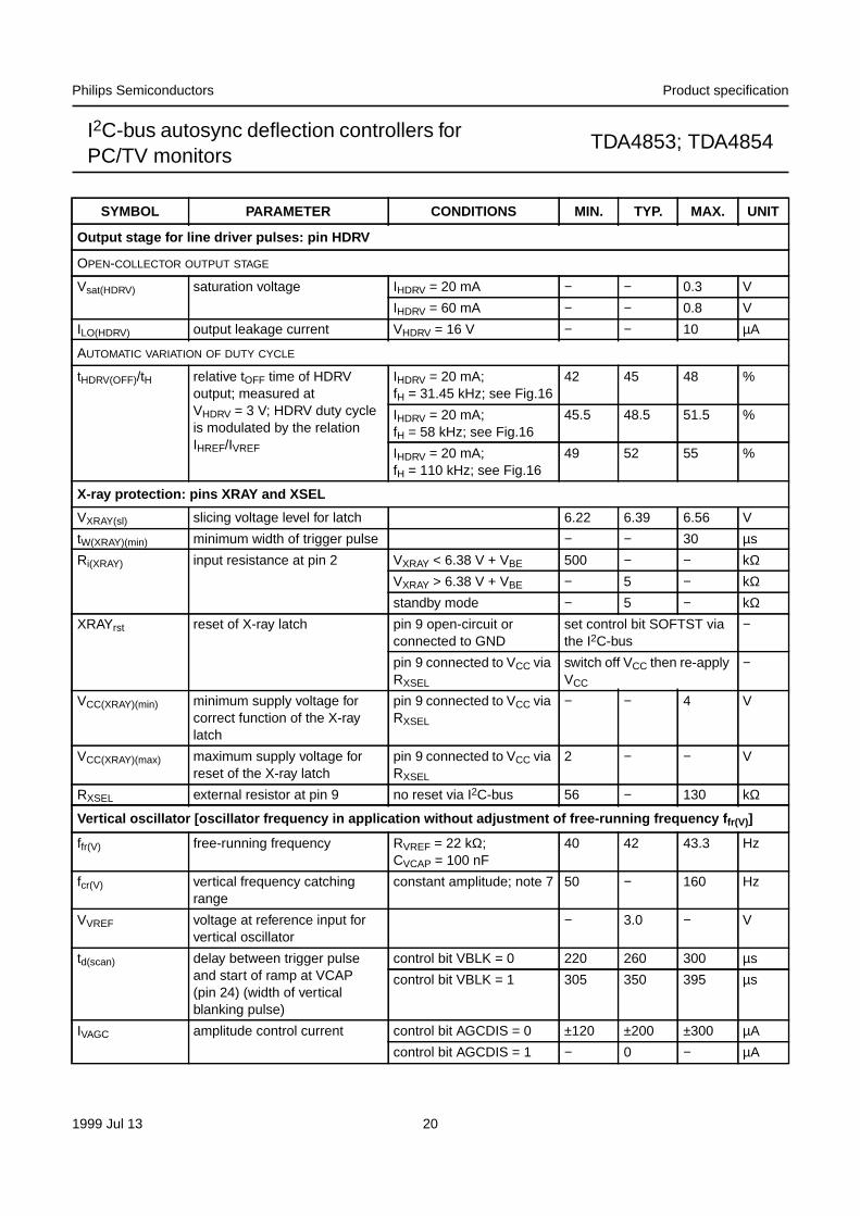
Output stage for line driver pulses: pin HDRV
OPEN-COLLECTOR OUTPUT STAGE
Vsat(HDRV) saturation voltage IHDRV = 20 mA − − 0.3 V
IHDRV = 60 mA − − 0.8 V
ILO(HDRV) output leakage current VHDRV = 16 V − − 10 µA
AUTOMATIC VARIATION OF DUTY CYCLE
tHDRV(OFF)/tH relative tOFF time of HDRVoutput; measured atVHDRV = 3 V; HDRV duty cycleis modulated by the relationIHREF/IVREF
IHDRV = 20 mA;fH = 31.45 kHz; see Fig.16
42 45 48 %
IHDRV = 20 mA;fH = 58 kHz; see Fig.16
45.5 48.5 51.5 %
IHDRV = 20 mA;fH = 110 kHz; see Fig.16
49 52 55 %
X-ray protection: pins XRAY and XSEL
VXRAY(sl) slicing voltage level for latch 6.22 6.39 6.56 V
tW(XRAY)(min) minimum width of trigger pulse − − 30 µs
Ri(XRAY) input resistance at pin 2 VXRAY < 6.38 V + VBE 500 − − kΩVXRAY > 6.38 V + VBE − 5 − kΩstandby mode − 5 − kΩ
XRAYrst reset of X-ray latch pin 9 open-circuit orconnected to GND
set control bit SOFTST viathe I2C-bus
−
pin 9 connected to VCC viaRXSEL
switch off VCC then re-applyVCC
−
VCC(XRAY)(min) minimum supply voltage forcorrect function of the X-raylatch
pin 9 connected to VCC viaRXSEL
− − 4 V
VCC(XRAY)(max) maximum supply voltage forreset of the X-ray latch
pin 9 connected to VCC viaRXSEL
2 − − V
RXSEL external resistor at pin 9 no reset via I2C-bus 56 − 130 kΩ
Vertical oscillator [oscillator frequency in application without adjustment of free-running frequency f fr(V)]
ffr(V) free-running frequency RVREF = 22 kΩ;CVCAP = 100 nF
40 42 43.3 Hz
fcr(V) vertical frequency catchingrange
constant amplitude; note 7 50 − 160 Hz
VVREF voltage at reference input forvertical oscillator
− 3.0 − V
td(scan) delay between trigger pulseand start of ramp at VCAP(pin 24) (width of verticalblanking pulse)
control bit VBLK = 0 220 260 300 µs
control bit VBLK = 1 305 350 395 µs
IVAGC amplitude control current control bit AGCDIS = 0 ±120 ±200 ±300 µA
control bit AGCDIS = 1 − 0 − µA
SYMBOL PARAMETER CONDITIONS MIN. TYP. MAX. UNIT
1999 Jul 13 21
Philips Semiconductors Product specification
I2C-bus autosync deflection controllers forPC/TV monitors
TDA4853; TDA4854
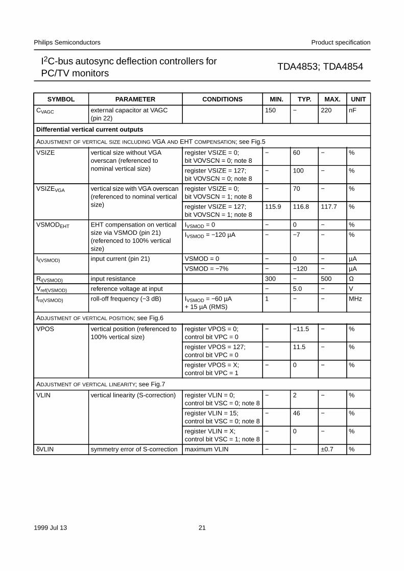
CVAGC external capacitor at VAGC(pin 22)
150 − 220 nF
Differential vertical current outputs
ADJUSTMENT OF VERTICAL SIZE INCLUDING VGA AND EHT COMPENSATION; see Fig.5
VSIZE vertical size without VGAoverscan (referenced tonominal vertical size)
register VSIZE = 0;bit VOVSCN = 0; note 8
− 60 − %
register VSIZE = 127;bit VOVSCN = 0; note 8
− 100 − %
VSIZEVGA vertical size with VGA overscan(referenced to nominal verticalsize)
register VSIZE = 0;bit VOVSCN = 1; note 8
− 70 − %
register VSIZE = 127;bit VOVSCN = 1; note 8
115.9 116.8 117.7 %
VSMODEHT EHT compensation on verticalsize via VSMOD (pin 21)(referenced to 100% verticalsize)
IVSMOD = 0 − 0 − %
IVSMOD = −120 µA − −7 − %
Ii(VSMOD) input current (pin 21) VSMOD = 0 − 0 − µA
VSMOD = −7% − −120 − µA
Ri(VSMOD) input resistance 300 − 500 ΩVref(VSMOD) reference voltage at input − 5.0 − V
fro(VSMOD) roll-off frequency (−3 dB) IVSMOD = −60 µA+ 15 µA (RMS)
1 − − MHz
ADJUSTMENT OF VERTICAL POSITION; see Fig.6
VPOS vertical position (referenced to100% vertical size)
register VPOS = 0;control bit VPC = 0
− −11.5 − %
register VPOS = 127;control bit VPC = 0
− 11.5 − %
register VPOS = X;control bit VPC = 1
− 0 − %
ADJUSTMENT OF VERTICAL LINEARITY; see Fig.7
VLIN vertical linearity (S-correction) register VLIN = 0;control bit VSC = 0; note 8
− 2 − %
register VLIN = 15;control bit VSC = 0; note 8
− 46 − %
register VLIN = X;control bit VSC = 1; note 8
− 0 − %
δVLIN symmetry error of S-correction maximum VLIN − − ±0.7 %
SYMBOL PARAMETER CONDITIONS MIN. TYP. MAX. UNIT
1999 Jul 13 22
Philips Semiconductors Product specification
I2C-bus autosync deflection controllers forPC/TV monitors
TDA4853; TDA4854
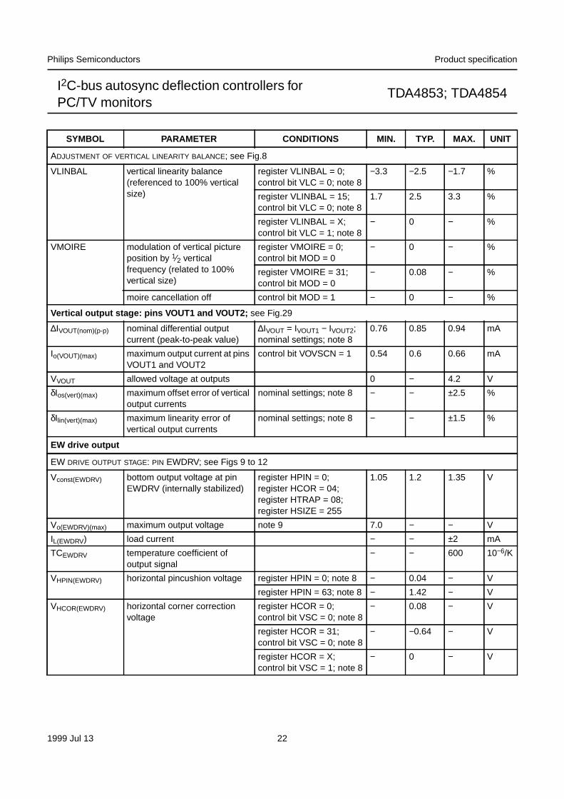
ADJUSTMENT OF VERTICAL LINEARITY BALANCE; see Fig.8
VLINBAL vertical linearity balance(referenced to 100% verticalsize)
register VLINBAL = 0;control bit VLC = 0; note 8
−3.3 −2.5 −1.7 %
register VLINBAL = 15;control bit VLC = 0; note 8
1.7 2.5 3.3 %
register VLINBAL = X;control bit VLC = 1; note 8
− 0 − %
VMOIRE modulation of vertical pictureposition by 1⁄2 verticalfrequency (related to 100%vertical size)
register VMOIRE = 0;control bit MOD = 0
− 0 − %
register VMOIRE = 31;control bit MOD = 0
− 0.08 − %
moire cancellation off control bit MOD = 1 − 0 − %
Vertical output stage: pins VOUT1 and VOUT2; see Fig.29
∆IVOUT(nom)(p-p) nominal differential outputcurrent (peak-to-peak value)
∆IVOUT = IVOUT1 − IVOUT2;nominal settings; note 8
0.76 0.85 0.94 mA
Io(VOUT)(max) maximum output current at pinsVOUT1 and VOUT2
control bit VOVSCN = 1 0.54 0.6 0.66 mA
VVOUT allowed voltage at outputs 0 − 4.2 V
δIos(vert)(max) maximum offset error of verticaloutput currents
nominal settings; note 8 − − ±2.5 %
δIlin(vert)(max) maximum linearity error ofvertical output currents
nominal settings; note 8 − − ±1.5 %
EW drive output
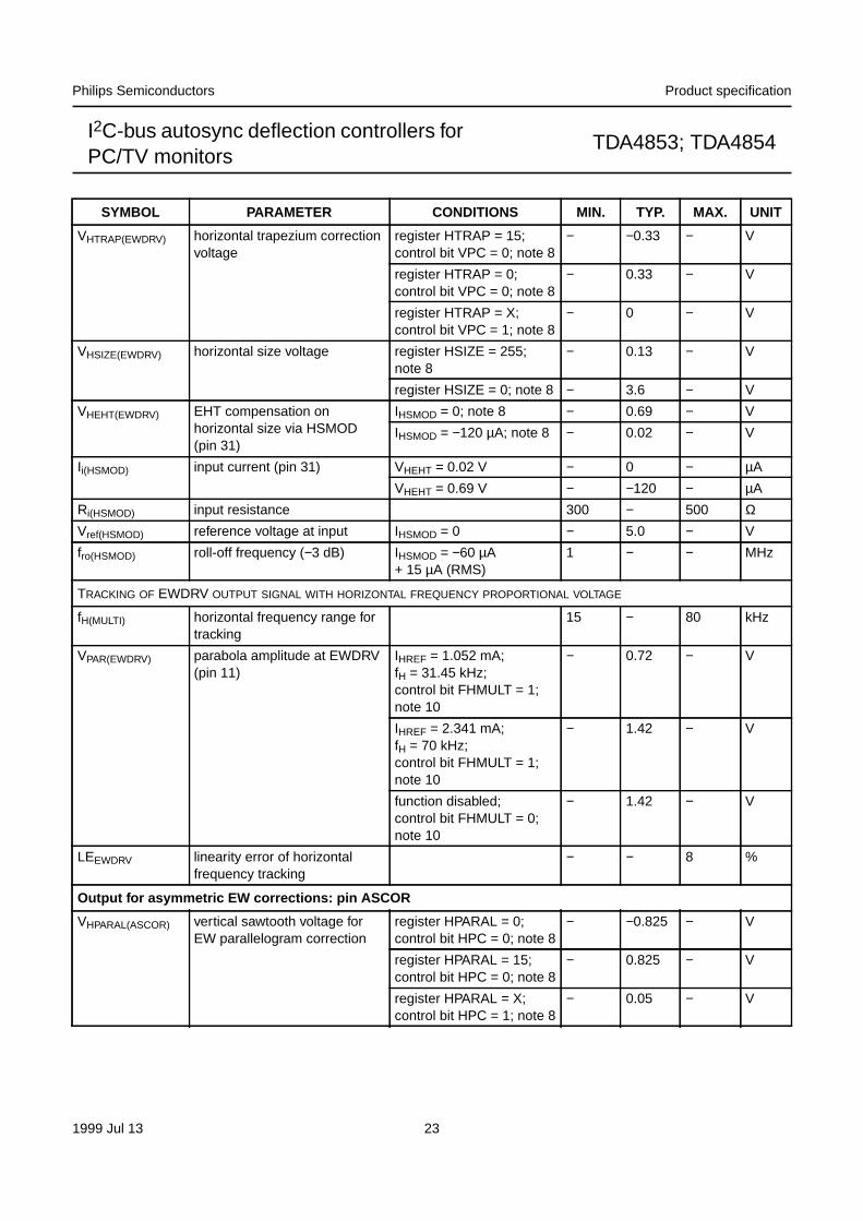
EW DRIVE OUTPUT STAGE: PIN EWDRV; see Figs 9 to 12
Vconst(EWDRV) bottom output voltage at pinEWDRV (internally stabilized)
register HPIN = 0;register HCOR = 04;register HTRAP = 08;register HSIZE = 255
1.05 1.2 1.35 V
Vo(EWDRV)(max) maximum output voltage note 9 7.0 − − V
IL(EWDRV) load current − − ±2 mA
TCEWDRV temperature coefficient ofoutput signal
− − 600 10−6/K
VHPIN(EWDRV) horizontal pincushion voltage register HPIN = 0; note 8 − 0.04 − V
register HPIN = 63; note 8 − 1.42 − V
VHCOR(EWDRV) horizontal corner correctionvoltage
register HCOR = 0;control bit VSC = 0; note 8
− 0.08 − V
register HCOR = 31;control bit VSC = 0; note 8
− −0.64 − V
register HCOR = X;control bit VSC = 1; note 8
− 0 − V
SYMBOL PARAMETER CONDITIONS MIN. TYP. MAX. UNIT
1999 Jul 13 23
Philips Semiconductors Product specification
I2C-bus autosync deflection controllers forPC/TV monitors
TDA4853; TDA4854
VHTRAP(EWDRV) horizontal trapezium correctionvoltage
register HTRAP = 15;control bit VPC = 0; note 8
− −0.33 − V
register HTRAP = 0;control bit VPC = 0; note 8
− 0.33 − V
register HTRAP = X;control bit VPC = 1; note 8
− 0 − V
VHSIZE(EWDRV) horizontal size voltage register HSIZE = 255;note 8
− 0.13 − V
register HSIZE = 0; note 8 − 3.6 − V
VHEHT(EWDRV) EHT compensation onhorizontal size via HSMOD(pin 31)
IHSMOD = 0; note 8 − 0.69 − V
IHSMOD = −120 µA; note 8 − 0.02 − V
Ii(HSMOD) input current (pin 31) VHEHT = 0.02 V − 0 − µA
VHEHT = 0.69 V − −120 − µA
Ri(HSMOD) input resistance 300 − 500 ΩVref(HSMOD) reference voltage at input IHSMOD = 0 − 5.0 − V
fro(HSMOD) roll-off frequency (−3 dB) IHSMOD = −60 µA+ 15 µA (RMS)
1 − − MHz
TRACKING OF EWDRV OUTPUT SIGNAL WITH HORIZONTAL FREQUENCY PROPORTIONAL VOLTAGE
fH(MULTI) horizontal frequency range fortracking
15 − 80 kHz
VPAR(EWDRV) parabola amplitude at EWDRV(pin 11)
IHREF = 1.052 mA;fH = 31.45 kHz;control bit FHMULT = 1;note 10
− 0.72 − V
IHREF = 2.341 mA;fH = 70 kHz;control bit FHMULT = 1;note 10
− 1.42 − V
function disabled;control bit FHMULT = 0;note 10
− 1.42 − V
LEEWDRV linearity error of horizontalfrequency tracking
− − 8 %
Output for asymmetric EW corrections: pin ASCOR
VHPARAL(ASCOR) vertical sawtooth voltage forEW parallelogram correction
register HPARAL = 0;control bit HPC = 0; note 8
− −0.825 − V
register HPARAL = 15;control bit HPC = 0; note 8
− 0.825 − V
register HPARAL = X;control bit HPC = 1; note 8
− 0.05 − V
SYMBOL PARAMETER CONDITIONS MIN. TYP. MAX. UNIT
1999 Jul 13 24
Philips Semiconductors Product specification
I2C-bus autosync deflection controllers forPC/TV monitors
TDA4853; TDA4854
VHPINBAL(ASCOR) vertical parabola voltage for pinunbalance correction
register HPINBAL = 0;control bit HBC = 0; note 8
− −1.0 − V
register HPINBAL = 15;control bit HBC = 0; note 8
− 1.0 − V
register HPINBAL = X;control bit HBC = 1; note 8
− 0.05 − V
Vo(ASCOR)(max)(p-p) maximum output voltage swing(peak-to-peak value)
− 4 − V
Vo(ASCOR)(max) maximum output voltage − 6.5 − V
Vc(ASCOR) centre voltage − 4.0 − V
Vo(ASCOR)(min) minimum output voltage − 1.9 − V
Io(ASCOR)(max) maximum output current VASCOR ≥ 1.9 V − −1.5 − mA
Io(sink)(ASCOR)(max) maximum output sink current VASCOR ≥ 1.9 V − 50 − µA
Focus section: pin FOCUS; TDA4854 only
VHFOCUS(p-p) amplitude of horizontalparabola (peak-to-peak value)
register HFOCUS = 0 − 0.06 − V
register HFOCUS = 31 − 3.2 − V
tprecor pre-correction of phase 1.9 µs < tfb < 5.5 µs − 350 − ns
tW(hfb)(min) minimum horizontal flybackpulse width
typical tprecor = 350 ns 1.9 − − µs
tW(hfb)(max) maximum horizontal flybackpulse width
typical tprecor = 350 ns − − 5.5 µs
tW(hfb)(TV)(max) maximum horizontal flybackpulse width (TV)
typical td = 300 ns − − 12.5 µs
VVFOCUS(p-p) amplitude of vertical parabola(peak-to-peak value)
register VFOCUS = 0;note 8
− 0.02 − V
register VFOCUS = 07;note 8
− 0.8 − V
Vo(FOCUS)(max) maximum output voltage IFOCUS = 0 5.7 6 6.3 V
Vo(FOCUS)(min) minimum output voltage IFOCUS = 0 1.7 2 2.3 V
Io(FOCUS)(max) maximum output current ±1.5 − − mA
CL(FOCUS)(max) maximum capacitive load − − 20 pF
B+ control section; see Figs 23 and 24
TRANSCONDUCTANCE AMPLIFIER: PINS BIN AND BOP
Vi(BIN) input voltage pin 5 0 − 5.25 V
Ii(BIN)(max) maximum input current pin 5 − − ±1 µA
Vref(int) reference voltage at internalnon-inverting input of OTA
2.37 2.5 2.58 V
Vo(BOP)(min) minimum output voltage pin 3 − − 0.5 V
Vo(BOP)(max) maximum output voltage pin 3 IBOP < 1 mA 5.0 5.3 5.6 V
Io(BOP)(max) maximum output current pin 3 − ±500 − µA
gm(OTA) transconductance of OTA note 11 30 50 70 mS
Gv(ol) open-loop voltage gain note 12 − 86 − dB
SYMBOL PARAMETER CONDITIONS MIN. TYP. MAX. UNIT
1999 Jul 13 25
Philips Semiconductors Product specification
I2C-bus autosync deflection controllers forPC/TV monitors
TDA4853; TDA4854
CBOP(min) minimum value of capacitor atpin 3
10 − − nF
VOLTAGE COMPARATOR: PIN BSENS
Vi(BSENS) voltage range of positivecomparator input
0 − 5 V
Vi(BOP) voltage range of negativecomparator input
0 − 5 V
IL(BSENS)(max) maximum leakage current discharge disabled − − −2 µA
OPEN-COLLECTOR OUTPUT STAGE: PIN BDRV
Io(BDRV)(max) maximum output current 20 − − mA
ILO(BDRV) output leakage current VBDRV = 16 V − − 3 µA
Vsat(BDRV) saturation voltage IBDRV < 20 mA − − 300 mV
toff(BDRV)(min) minimum off-time − 250 − ns
td(BDRV-HDRV) delay between BDRV pulseand HDRV pulse
measured atVHDRV = VBDRV = 3 V
− 500 − ns
BSENS DISCHARGE CIRCUIT: PIN BSENS
VSTOP(BSENS) discharge stop level capacitive load;IBSENS = 0.5 mA
0.85 1.0 1.15 V
Idch(BSENS) discharge current VBSENS > 2.5 V 4.5 6.0 7.5 mA
Vth(BSENS)(restart) threshold voltage for restart fault condition 1.2 1.3 1.4 V
CBSENS(min) minimum value of capacitor atBSENS (pin 4)
2 − − nF
Internal reference, supply voltage, soft start and protection
VCC(stab) external supply voltage forcomplete stabilization of allinternal references
9.2 − 16 V
ICC supply current − 70 − mA
ICC(stb) standby supply current STDBY = 1; VPLL2 < 1 V;3.5 V < VCC < 16 V
− 9 − mA
PSRR power supply rejection ratio ofinternal supply voltage
f = 1 kHz 50 − − dB
VCC(blank) supply voltage level foractivation of continuousblanking
VCC decreasing from 12 V 8.2 8.6 9.0 V
VCC(blank)(min) minimum supply voltage levelfor function of continuousblanking
VCC decreasing from 12 V 2.5 3.5 4.0 V
Von(VCC) supply voltage level foractivation of HDRV, BDRV,VOUT1, VOUT2 andHUNLOCK
VCC increasing from belowtypical 8 V
7.9 8.3 8.7 V
SYMBOL PARAMETER CONDITIONS MIN. TYP. MAX. UNIT
1999 Jul 13 26
Philips Semiconductors Product specification
I2C-bus autosync deflection controllers forPC/TV monitors
TDA4853; TDA4854
Notes
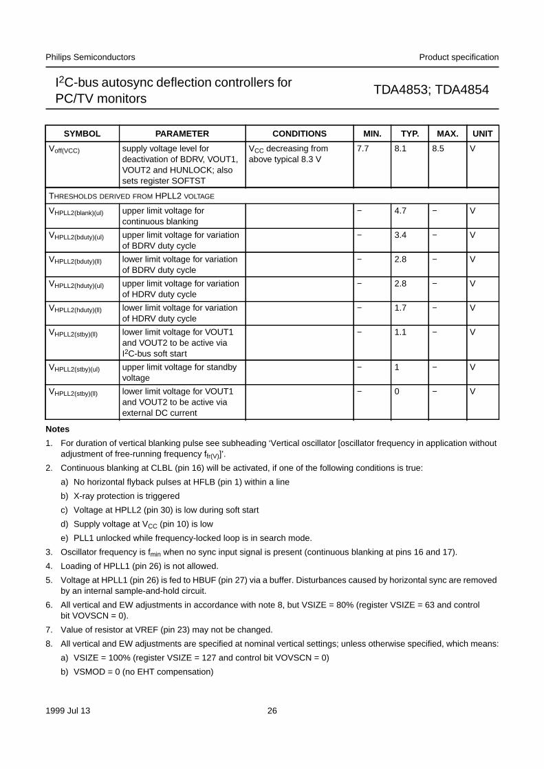
1. For duration of vertical blanking pulse see subheading ‘Vertical oscillator [oscillator frequency in application withoutadjustment of free-running frequency ffr(V)]’.
2. Continuous blanking at CLBL (pin 16) will be activated, if one of the following conditions is true:
a) No horizontal flyback pulses at HFLB (pin 1) within a line
b) X-ray protection is triggered
c) Voltage at HPLL2 (pin 30) is low during soft start
d) Supply voltage at VCC (pin 10) is low
e) PLL1 unlocked while frequency-locked loop is in search mode.
3. Oscillator frequency is fmin when no sync input signal is present (continuous blanking at pins 16 and 17).
4. Loading of HPLL1 (pin 26) is not allowed.
5. Voltage at HPLL1 (pin 26) is fed to HBUF (pin 27) via a buffer. Disturbances caused by horizontal sync are removedby an internal sample-and-hold circuit.
6. All vertical and EW adjustments in accordance with note 8, but VSIZE = 80% (register VSIZE = 63 and controlbit VOVSCN = 0).
7. Value of resistor at VREF (pin 23) may not be changed.
8. All vertical and EW adjustments are specified at nominal vertical settings; unless otherwise specified, which means:
a) VSIZE = 100% (register VSIZE = 127 and control bit VOVSCN = 0)
b) VSMOD = 0 (no EHT compensation)
Voff(VCC) supply voltage level fordeactivation of BDRV, VOUT1,VOUT2 and HUNLOCK; alsosets register SOFTST
VCC decreasing fromabove typical 8.3 V
7.7 8.1 8.5 V
THRESHOLDS DERIVED FROM HPLL2 VOLTAGE
VHPLL2(blank)(ul) upper limit voltage forcontinuous blanking
− 4.7 − V
VHPLL2(bduty)(ul) upper limit voltage for variationof BDRV duty cycle
− 3.4 − V
VHPLL2(bduty)(ll) lower limit voltage for variationof BDRV duty cycle
− 2.8 − V
VHPLL2(hduty)(ul) upper limit voltage for variationof HDRV duty cycle
− 2.8 − V
VHPLL2(hduty)(ll) lower limit voltage for variationof HDRV duty cycle
− 1.7 − V
VHPLL2(stby)(ll) lower limit voltage for VOUT1and VOUT2 to be active viaI2C-bus soft start
− 1.1 − V
VHPLL2(stby)(ul) upper limit voltage for standbyvoltage
− 1 − V
VHPLL2(stby)(ll) lower limit voltage for VOUT1and VOUT2 to be active viaexternal DC current
− 0 − V
SYMBOL PARAMETER CONDITIONS MIN. TYP. MAX. UNIT
1999 Jul 13 27
Philips Semiconductors Product specification
I2C-bus autosync deflection controllers forPC/TV monitors
TDA4853; TDA4854
c) VPOS centred (register VPOS = X and controlbit VPC = 1)
d) VLIN = 0 (register VLIN = X and controlbit VSC = 1)
e) VLINBAL = 0 (register VLINBAL = X and controlbit VLC = 1)
f) FHMULT = 0
g) HPARAL = 0 (register HPARAL = X and controlbit HPC = 1)
h) HPINBAL = 0 (register HPINBAL = X and controlbit HBC = 1)
i) Vertical oscillator synchronized
j) HSIZE = 255.
9. The output signal at EWDRV (pin 11) may consist ofhorizontal pincushion + corner correction + DC shift +trapezium correction. If the control bit VOVSCN is set,and the VPOS adjustment is set to an extreme value,the tip of the parabola may be clipped at the upper limitof the EWDRV output voltage range. The waveform ofcorner correction will clip if the vertical sawtoothadjustment exceeds 110% of the nominal setting.
10. If fH tracking is enabled, the amplitude of the completeEWDRV output signal (horizontal pincushion + cornercorrection + DC shift + trapezium) will be changedproportional to IHREF. The EWDRV low level of 1.2 Vremains fixed.
11. First pole of transconductance amplifier is 5 MHzwithout external capacitor (will become the secondpole, if the OTA operates as an integrator).
12. Open-loop gain is at f = 0 with no resistive load
and CBOP = 10 nF [from BOP (pin 3) to GND].
VBOP
VBIN--------------
Vertical and EW adjustments
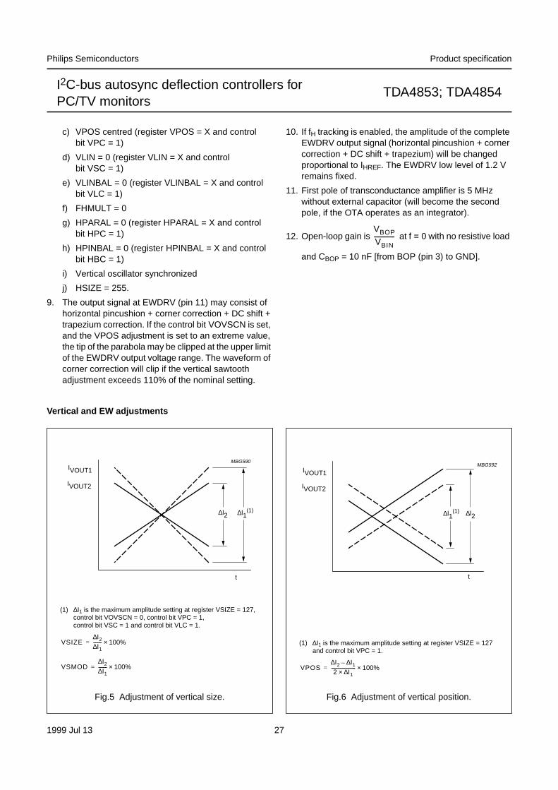
Fig.5 Adjustment of vertical size.
(1) ∆I1 is the maximum amplitude setting at register VSIZE = 127,control bit VOVSCN = 0, control bit VPC = 1,control bit VSC = 1 and control bit VLC = 1.
VSIZEI∆ 2
I∆ 1-------- 100%×=
VSMODI∆ 2
I∆ 1-------- 100%×=
handbook, halfpage
t
IVOUT1
IVOUT2
∆l2 ∆l1(1)
MBG590
Fig.6 Adjustment of vertical position.
(1) ∆I1 is the maximum amplitude setting at register VSIZE = 127and control bit VPC = 1.
VPOSI2∆ I1∆–
2 I1∆×---------------------- 100%×=
handbook, halfpage
t
IVOUT1
IVOUT2
∆l2∆l1(1)
MBG592
1999 Jul 13 28
Philips Semiconductors Product specification
I2C-bus autosync deflection controllers forPC/TV monitors
TDA4853; TDA4854
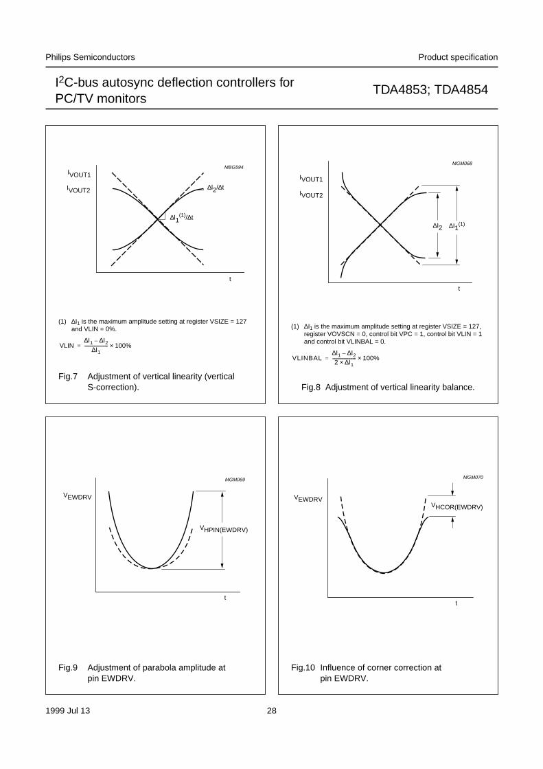
Fig.7 Adjustment of vertical linearity (verticalS-correction).
(1) ∆I1 is the maximum amplitude setting at register VSIZE = 127and VLIN = 0%.
VLINI∆ 1 I∆ 2–
I1∆---------------------- 100%×=
handbook, halfpage
t
IVOUT1
IVOUT2 ∆l2/∆t
∆l1(1)/∆t
MBG594
Fig.8 Adjustment of vertical linearity balance.
(1) ∆I1 is the maximum amplitude setting at register VSIZE = 127,register VOVSCN = 0, control bit VPC = 1, control bit VLIN = 1and control bit VLINBAL = 0.
VLINBALI∆ 1 I∆ 2–
2 I1∆×---------------------- 100%×=
handbook, halfpage
t
IVOUT1
IVOUT2
∆I1(1)∆I2
MGM068
Fig.9 Adjustment of parabola amplitude atpin EWDRV.
handbook, halfpage
t
VEWDRV
VHPIN(EWDRV)
MGM069
Fig.10 Influence of corner correction atpin EWDRV.
handbook, halfpage
t
VEWDRVVHCOR(EWDRV)
MGM070
1999 Jul 13 29
Philips Semiconductors Product specification
I2C-bus autosync deflection controllers forPC/TV monitors
TDA4853; TDA4854
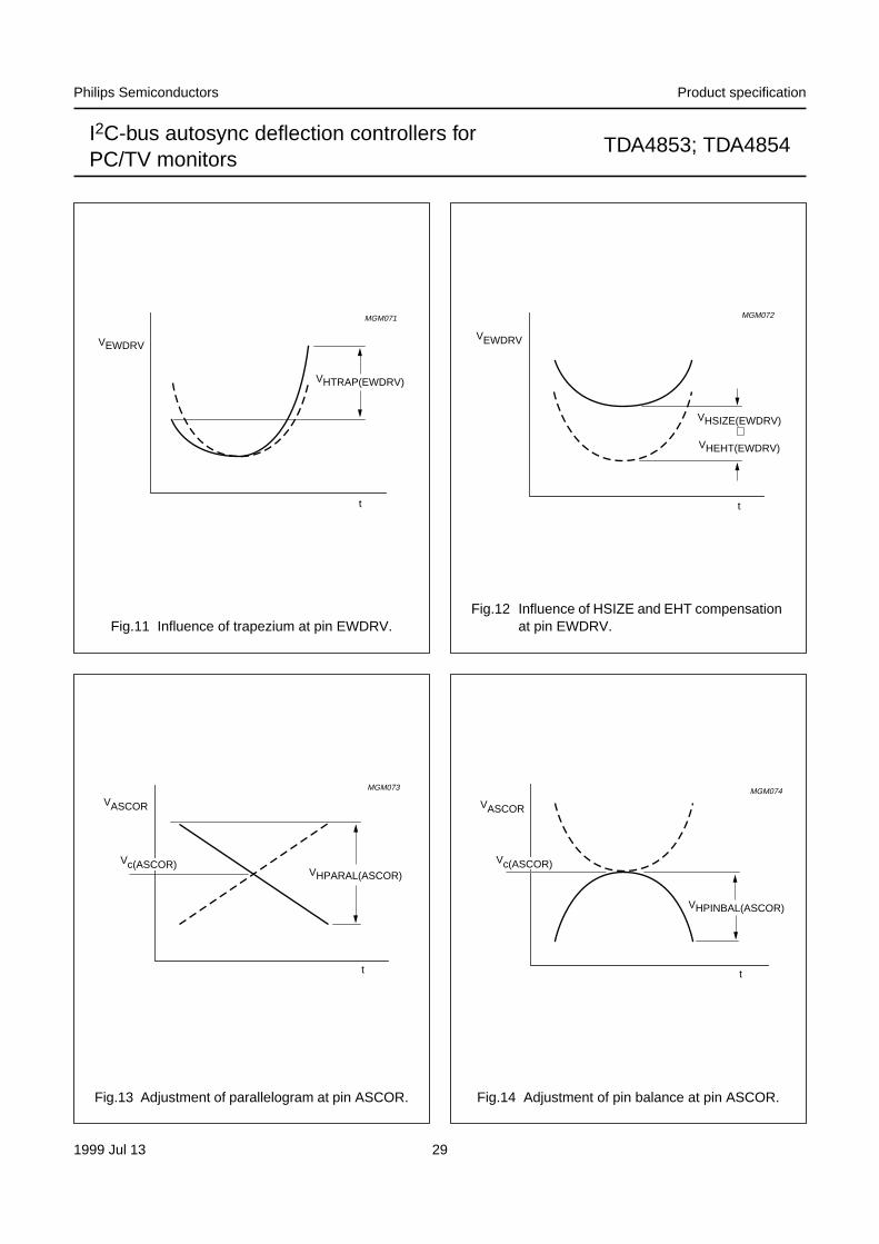
Fig.11 Influence of trapezium at pin EWDRV.
handbook, halfpage
t
VEWDRV
VHTRAP(EWDRV)
MGM071
Fig.12 Influence of HSIZE and EHT compensationat pin EWDRV.
handbook, halfpage
t
VEWDRV
VHSIZE(EWDRV)+
VHEHT(EWDRV)
MGM072
Fig.13 Adjustment of parallelogram at pin ASCOR.
handbook, halfpage
t
VHPARAL(ASCOR)
MGM073
VASCOR
Vc(ASCOR)
Fig.14 Adjustment of pin balance at pin ASCOR.
handbook, halfpage
t
VASCOR
VHPINBAL(ASCOR)
MGM074
Vc(ASCOR)
1999 Jul 13 30
Philips Semiconductors Product specification
I2C-bus autosync deflection controllers forPC/TV monitors
TDA4853; TDA4854
Pulse diagrams
handbook, full pagewidth
internal triggerinhibit window(typical 4 ms)
1.4 V
3.8 Vautomatic trigger level
vertical sync pulse
4.0 V
differential output currents VOUT1 (pin 13) and
VOUT2 (pin 12)
inhibited
vertical oscillator sawtoothat VCAP (pin 24)
vertical blanking pulseat CLBL (pin 16)
vertical blanking pulseat HUNLOCK (pin 17)
synchronized trigger level
EW drive waveformat EWDRV (pin 11)
DC shift 3.6 V maximum
7.0 V maximum
low-level 1.2 V fixed
IVOUT1
IVOUT2
MGM075
Fig.15 Pulse diagram for vertical part.
1999 Jul 13 31
Philips Semiconductors Product specification
I2C-bus autosync deflection controllers forPC/TV monitors
TDA4853; TDA4854
handbook, full pagewidth
+ -
+ –
horizontal sync pulse
PLL2 control currentat HPLL2 (pin 30)
PLL1 control currentat HPLL1 (pin 26)
line flyback pulseat HFLB (pin 1)
horizontal oscillator sawtoothat HCAP (pin 29)
line drive pulseat HDRV (pin 8)
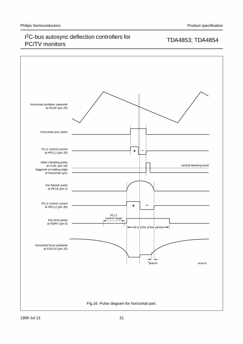
triggered on trailing edgeof horizontal sync
video clamping pulseat CLBL (pin 16) vertical blanking level
horizontal focus parabolaat FOCUS (pin 32)
PLL2control range
45 to 52% of line period
tprecor MGM076
Fig.16 Pulse diagram for horizontal part.
1999 Jul 13 32
Philips Semiconductors Product specification
I2C-bus autosync deflection controllers forPC/TV monitors
TDA4853; TDA4854
handbook, full pagewidth relative tHDRV(OFF)/tH(%)
MGM077
52
45
15 30 110 130 fH (kHz)
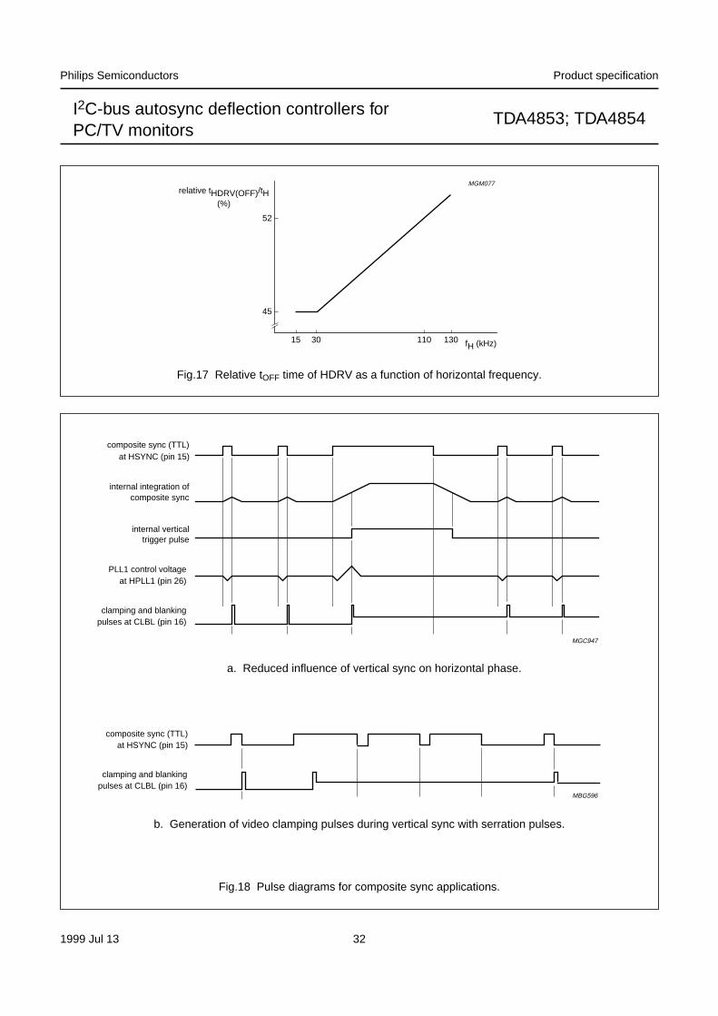
Fig.17 Relative tOFF time of HDRV as a function of horizontal frequency.
handbook, full pagewidthcomposite sync (TTL)
at HSYNC (pin 15)
clamping and blankingpulses at CLBL (pin 16)
MBG596
Fig.18 Pulse diagrams for composite sync applications.
a. Reduced influence of vertical sync on horizontal phase.
b. Generation of video clamping pulses during vertical sync with serration pulses.
handbook, full pagewidthcomposite sync (TTL)
internal integration ofcomposite sync
internal verticaltrigger pulse
PLL1 control voltageat HPLL1 (pin 26)
at HSYNC (pin 15)
pulses at CLBL (pin 16)clamping and blanking
MGC947
1999 Jul 13 33
Philips Semiconductors Product specification
I2C-bus autosync deflection controllers forPC/TV monitors
TDA4853; TDA4854
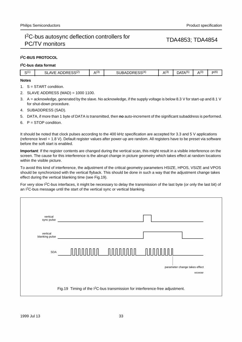
I2C-BUS PROTOCOL
I2C-bus data format
Notes
1. S = START condition.
2. SLAVE ADDRESS (MAD) = 1000 1100.
3. A = acknowledge, generated by the slave. No acknowledge, if the supply voltage is below 8.3 V for start-up and 8.1 Vfor shut-down procedure.
4. SUBADDRESS (SAD).
5. DATA, if more than 1 byte of DATA is transmitted, then no auto-increment of the significant subaddress is performed.
6. P = STOP condition.
It should be noted that clock pulses according to the 400 kHz specification are accepted for 3.3 and 5 V applications(reference level = 1.8 V). Default register values after power-up are random. All registers have to be preset via softwarebefore the soft start is enabled.
Important : If the register contents are changed during the vertical scan, this might result in a visible interference on thescreen. The cause for this interference is the abrupt change in picture geometry which takes effect at random locationswithin the visible picture.
To avoid this kind of interference, the adjustment of the critical geometry parameters HSIZE, HPOS, VSIZE and VPOSshould be synchronized with the vertical flyback. This should be done in such a way that the adjustment change takeseffect during the vertical blanking time (see Fig.19).
For very slow I2C-bus interfaces, it might be necessary to delay the transmission of the last byte (or only the last bit) ofan I2C-bus message until the start of the vertical sync or vertical blanking.
S(1) SLAVE ADDRESS(2) A(3) SUBADDRESS(4) A(3) DATA(5) A(3) P(6)
Fig.19 Timing of the I2C-bus transmission for interference-free adjustment.
handbook, full pagewidth
MGM088
verticalsync pulse
verticalblanking pulse
SDA
parameter change takes effect
1999 Jul 13 34
Philips Semiconductors Product specification
I2C-bus autosync deflection controllers forPC/TV monitors
TDA4853; TDA4854
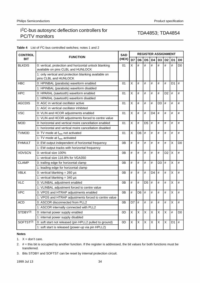
Table 4 List of I2C-bus controlled switches; notes 1 and 2
Notes
1. X = don’t care.
2. # = this bit is occupied by another function. If the register is addressed, the bit values for both functions must betransferred.
3. Bits STDBY and SOFTST can be reset by internal protection circuit.
CONTROLBIT
FUNCTIONSAD
(HEX)
REGISTER ASSIGNMENT
D7 D6 D5 D4 D3 D2 D1 D0
BLKDIS 0: vertical, protection and horizontal unlock blankingavailable on pins CLBL and HUNLOCK
01 X # # # # # # D0
1: only vertical and protection blanking available onpins CLBL and HUNLOCK
HBC 0: HPINBAL (parabola) waveform enabled 01 X # # # # # D1 #
1: HPINBAL (parabola) waveform disabled
HPC 0: HPARAL (sawtooth) waveform enabled 01 X # # # # D2 # #
1: HPARAL (sawtooth) waveform disabled
AGCDIS 0: AGC in vertical oscillator active 01 X # # # D3 # # #
1: AGC in vertical oscillator inhibited
VSC 0: VLIN and HCOR adjustments enabled 01 X # # D4 # # # #
1: VLIN and HCOR adjustments forced to centre value
MOD 0: horizontal and vertical moire cancellation enabled 01 X # D5 # # # # #
1: horizontal and vertical moire cancellation disabled
TVMOD 0: TV mode at fmin not activated 01 X D6 # # # # # #
1: TV mode at fmin activated
FHMULT 0: EW output independent of horizontal frequency 0B # # # # # # X D0
1: EW output tracks with horizontal frequency
VOVSCN 0: vertical size 100% 0B # # # # # D2 X #
1: vertical size 116.8% for VGA350
CLAMP 0: trailing edge for horizontal clamp 0B # # # # D3 # X #
1: leading edge for horizontal clamp
VBLK 0: vertical blanking = 260 µs 0B # # # D4 # # X #
1: vertical blanking = 340 µs
VLC 0: VLINBAL adjustment enabled 0B # # D5 # # # X #
1: VLINBAL adjustment forced to centre value
VPC 0: VPOS and HTRAP adjustments enabled 0B # D6 # # # # X #
1: VPOS and HTRAP adjustments forced to centre value
ACD 0: ASCOR disconnected from PLL2 0B D7 # # # # # X #
1: ASCOR internally connected with PLL2
STDBY(3) 0: internal power supply enabled 0D X X X X X X # D0
1: internal power supply disabled
SOFTST(3) 0: soft start not released (pin HPLL2 pulled to ground) 0D X X X X X X D1 #
1: soft start is released (power-up via pin HPLL2)
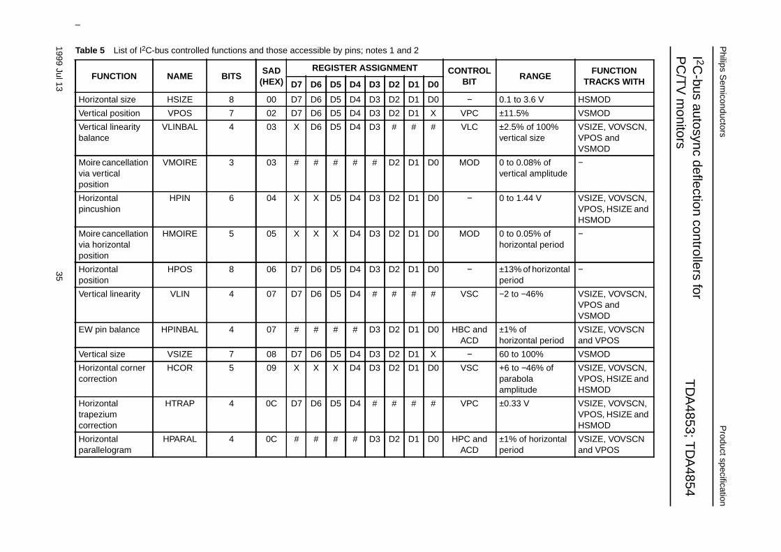
1999Jul13
35
Philips S
emiconductors
Product specification
I 2C-bus autosync deflection controllers for
PC
/TV
monitors
TD
A4853; T
DA
4854
This text is here in white to force landscape pages to be rotated correctly when browsing through the pdf in the Acrobat reader.This text is here in_white to force landscape pages to be rotated correctly when browsing through the pdf in the Acrobat reader.This text is here inThis text is here inwhite to force landscape pages to be rotated correctly when browsing through the pdf in the Acrobat reader. white to force landscape pages to be ...
Table 5 List of I2C-bus controlled functions and those accessible by pins; notes 1 and 2
FUNCTION NAME BITSSAD
(HEX)
REGISTER ASSIGNMENT CONTROLBIT
RANGEFUNCTION
TRACKS WITHD7 D6 D5 D4 D3 D2 D1 D0
Horizontal size HSIZE 8 00 D7 D6 D5 D4 D3 D2 D1 D0 − 0.1 to 3.6 V HSMOD
Vertical position VPOS 7 02 D7 D6 D5 D4 D3 D2 D1 X VPC ±11.5% VSMOD
Vertical linearitybalance
VLINBAL 4 03 X D6 D5 D4 D3 # # # VLC ±2.5% of 100%vertical size
VSIZE, VOVSCN,VPOS andVSMOD
Moire cancellationvia verticalposition
VMOIRE 3 03 # # # # # D2 D1 D0 MOD 0 to 0.08% ofvertical amplitude
−
Horizontalpincushion
HPIN 6 04 X X D5 D4 D3 D2 D1 D0 − 0 to 1.44 V VSIZE, VOVSCN,VPOS, HSIZE andHSMOD
Moire cancellationvia horizontalposition
HMOIRE 5 05 X X X D4 D3 D2 D1 D0 MOD 0 to 0.05% ofhorizontal period
−
Horizontalposition
HPOS 8 06 D7 D6 D5 D4 D3 D2 D1 D0 − ±13% of horizontalperiod
−
Vertical linearity VLIN 4 07 D7 D6 D5 D4 # # # # VSC −2 to −46% VSIZE, VOVSCN,VPOS andVSMOD
EW pin balance HPINBAL 4 07 # # # # D3 D2 D1 D0 HBC andACD
±1% ofhorizontal period
VSIZE, VOVSCNand VPOS
Vertical size VSIZE 7 08 D7 D6 D5 D4 D3 D2 D1 X − 60 to 100% VSMOD
Horizontal cornercorrection
HCOR 5 09 X X X D4 D3 D2 D1 D0 VSC +6 to −46% ofparabolaamplitude
VSIZE, VOVSCN,VPOS, HSIZE andHSMOD
Horizontaltrapeziumcorrection
HTRAP 4 0C D7 D6 D5 D4 # # # # VPC ±0.33 V VSIZE, VOVSCN,VPOS, HSIZE andHSMOD
Horizontalparallelogram
HPARAL 4 0C # # # # D3 D2 D1 D0 HPC andACD
±1% of horizontalperiod
VSIZE, VOVSCNand VPOS
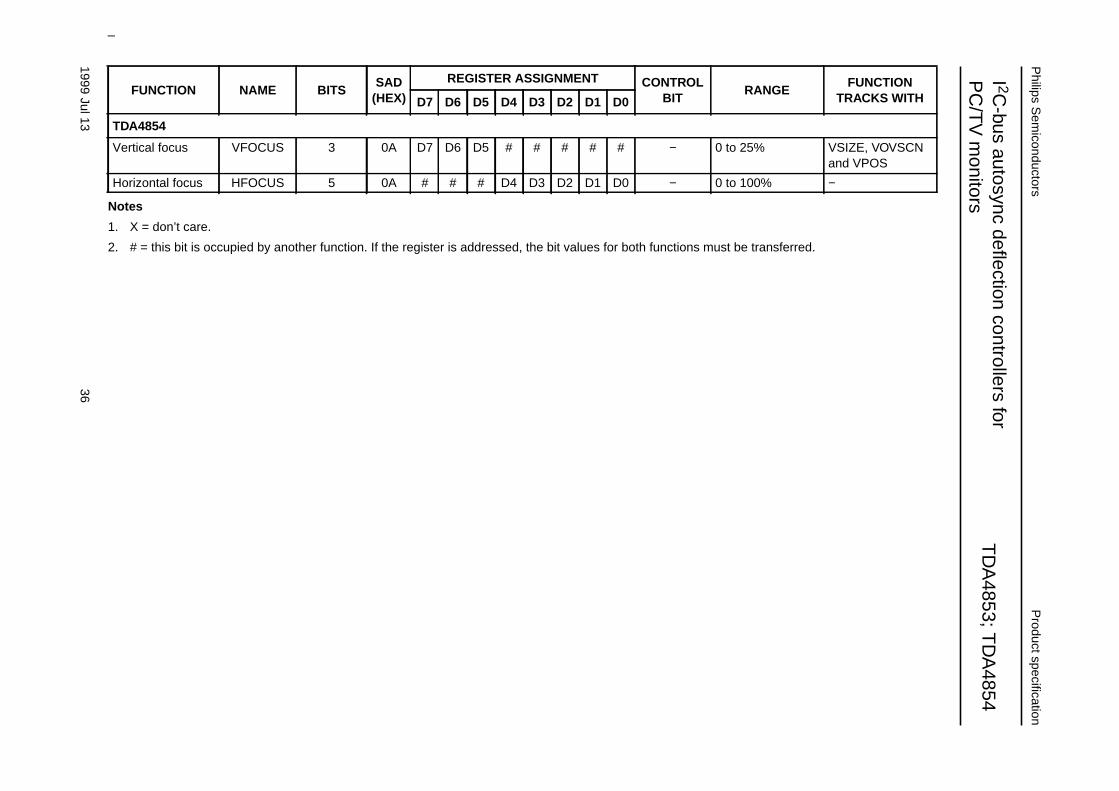
1999Jul13
36
Philips S
emiconductors
Product specification
I 2C-bus autosync deflection controllers for
PC
/TV
monitors
TD
A4853; T
DA
4854
This text is here in white to force landscape pages to be rotated correctly when browsing through the pdf in the Acrobat reader.This text is here in_white to force landscape pages to be rotated correctly when browsing through the pdf in the Acrobat reader.This text is here inThis text is here inwhite to force landscape pages to be rotated correctly when browsing through the pdf in the Acrobat reader. white to force landscape pages to be ...
Notes
1. X = don’t care.
2. # = this bit is occupied by another function. If the register is addressed, the bit values for both functions must be transferred.
TDA4854
Vertical focus VFOCUS 3 0A D7 D6 D5 # # # # # − 0 to 25% VSIZE, VOVSCNand VPOS
Horizontal focus HFOCUS 5 0A # # # D4 D3 D2 D1 D0 − 0 to 100% −
FUNCTION NAME BITSSAD
(HEX)
REGISTER ASSIGNMENT CONTROLBIT
RANGEFUNCTION
TRACKS WITHD7 D6 D5 D4 D3 D2 D1 D0
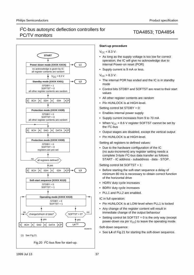
1999 Jul 13 37
Philips Semiconductors Product specification
I2C-bus autosync deflection controllers forPC/TV monitors
TDA4853; TDA4854
Start-up procedure
VCC < 8.3 V:
• As long as the supply voltage is too low for correctoperation, the IC will give no acknowledge due tointernal Power-on reset (POR)
• Supply current is 9 mA or less.
VCC > 8.3 V:
• The internal POR has ended and the IC is in standbymode
• Control bits STDBY and SOFTST are reset to their startvalues
• All other register contents are random
• Pin HUNLOCK is at HIGH-level.
Setting control bit STDBY = 0:
• Enables internal power supply
• Supply current increases from 9 to 70 mA
• When VCC < 8.6 V register SOFTST cannot be set bythe I2C-bus
• Output stages are disabled, except the vertical output
• Pin HUNLOCK is at HIGH-level.
Setting all registers to defined values:
• Due to the hardware configuration of the IC(no auto-increment) any register setting needs acomplete 3-byte I2C-bus data transfer as follows:START - IC address - subaddress - data - STOP.
Setting control bit SOFTST = 1:
• Before starting the soft-start sequence a delay ofminimum 80 ms is necessary to obtain correct functionof the horizontal drive
• HDRV duty cycle increases
• BDRV duty cycle increases
• PLL1 and PLL2 are enabled.
IC in full operation:
• Pin HUNLOCK is at LOW-level when PLL1 is locked
• Any change of the register content will result inimmediate change of the output behaviour
• Setting control bit SOFTST = 0 is the only way (exceptpower-down via pin VCC) to leave the operating mode.
Soft-down sequence:
• See L4 of Fig.21 for starting the soft-down sequence.
Fig.20 I2C-bus flow for start-up.
(1) See Fig.21.
MGM078
START
Standby mode (XXXX XX01)
STDBY = 1SOFTST = 0
all other register contents are random
Protection mode (XXXX XX00)
STDBY = 0SOFTST = 0
all other register contents are random
Protection mode (XXXX XX00)
STDBY = 0SOFTST = 0
registers are pre-set
change/refresh of data?
S 8CH A 0DH A 00H A P
S 8CH A 0DH A 02H A P
S 8CH A SAD A DATA A P
S 8CH A SAD A DATA A P
Operating mode (XXXX XX10)
STDBY = 0SOFTST = 1
Soft-start sequence (XXXX XX10)
STDBY = 0SOFTST = 1
Power-down mode (XXXX XXXX)
no acknowledge is given by ICall register contents are random
L1
L2
L3
L4 (1)
VCC > 8.3 V
no
yes
SOFTST = 0?no
yes
all registers defined?no
yes
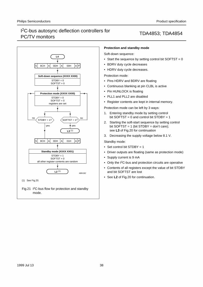
1999 Jul 13 38
Philips Semiconductors Product specification
I2C-bus autosync deflection controllers forPC/TV monitors
TDA4853; TDA4854
Protection and standby mode
Soft-down sequence:
• Start the sequence by setting control bit SOFTST = 0
• BDRV duty cycle decreases
• HDRV duty cycle decreases.
Protection mode:
• Pins HDRV and BDRV are floating
• Continuous blanking at pin CLBL is active
• Pin HUNLOCK is floating
• PLL1 and PLL2 are disabled
• Register contents are kept in internal memory.
Protection mode can be left by 3 ways:
1. Entering standby mode by setting controlbit SOFTST = 0 and control bit STDBY = 1
2. Starting the soft-start sequence by setting controlbit SOFTST = 1 (bit STDBY = don’t care);see L3 of Fig.20 for continuation
3. Decreasing the supply voltage below 8.1 V.
Standby mode:
• Set control bit STDBY = 1
• Driver outputs are floating (same as protection mode)
• Supply current is 9 mA
• Only the I2C-bus and protection circuits are operative
• Contents of all registers except the value of bit STDBYand bit SOFTST are lost
• See L2 of Fig.20 for continuation.MBK382
Standby mode (XXXX XX01)
STDBY = 1SOFTST = 0
all other register contents are random
Soft-down sequence (XXXX XX00)
STDBY = 0SOFTST = 0
L4
L3 (1)
no
yes
SOFTST = 1?
yes
L2 (1)
Protection mode (XXXX XX00)
STDBY = 0SOFTST = 0
registers are set
noSTDBY = 1?
S 8CH A 0DH A 00H A P
S 8CH A 0DH A 01H A P
Fig.21 I2C-bus flow for protection and standbymode.
(1) See Fig.20.
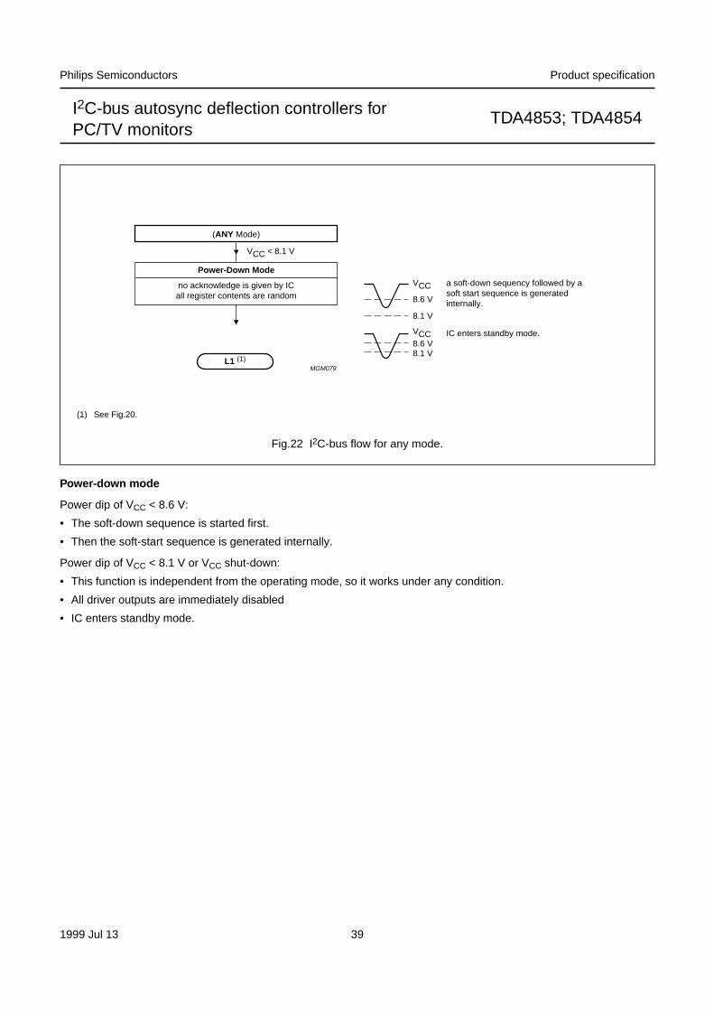
1999 Jul 13 39
Philips Semiconductors Product specification
I2C-bus autosync deflection controllers forPC/TV monitors
TDA4853; TDA4854
handbook, full pagewidth
MGM079
(ANY Mode)
Power-Down Mode
no acknowledge is given by ICall register contents are random
L1 (1)
VCC < 8.1 V
VCC a soft-down sequency followed by asoft start sequence is generatedinternally.8.6 V
8.1 V
VCC IC enters standby mode.8.6 V8.1 V
Fig.22 I2C-bus flow for any mode.
(1) See Fig.20.
Power-down mode
Power dip of VCC < 8.6 V:
• The soft-down sequence is started first.
• Then the soft-start sequence is generated internally.
Power dip of VCC < 8.1 V or VCC shut-down:
• This function is independent from the operating mode, so it works under any condition.
• All driver outputs are immediately disabled
• IC enters standby mode.
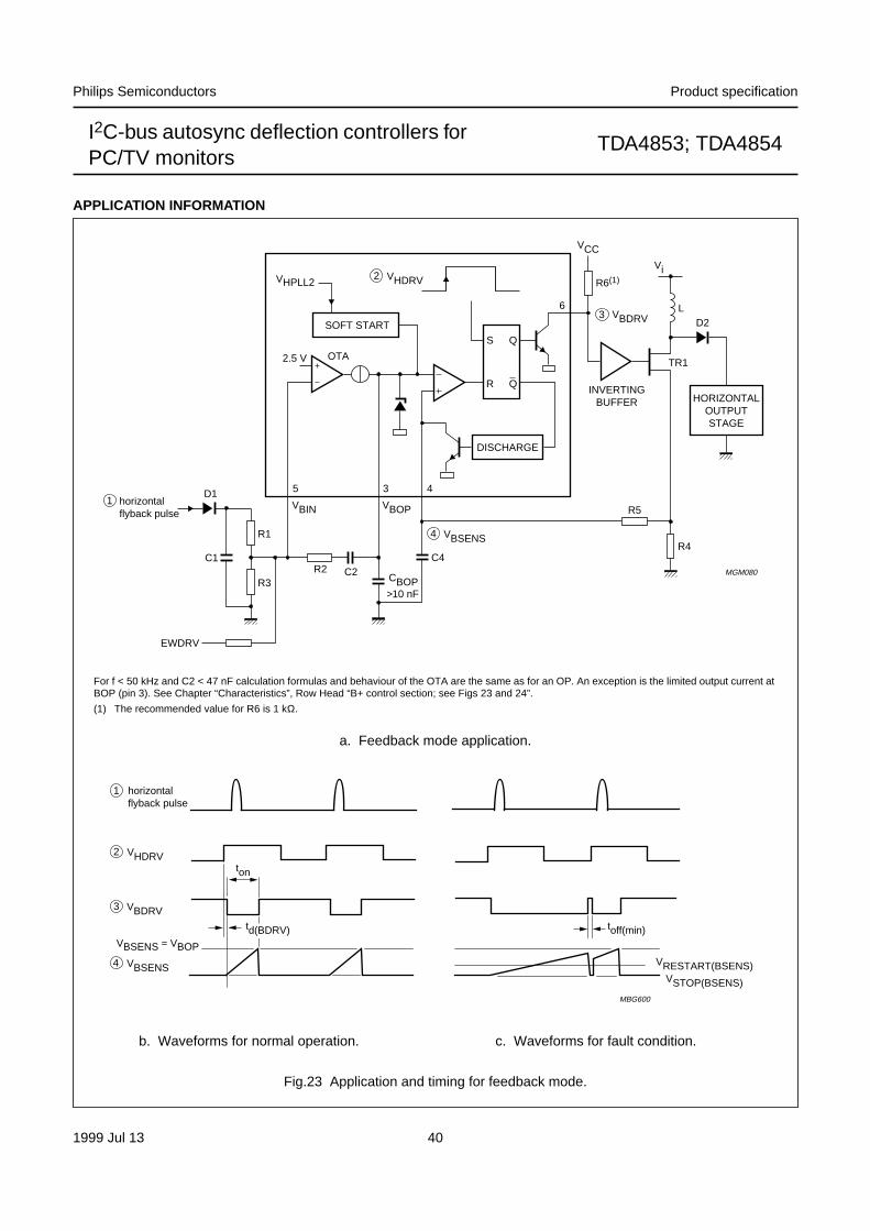
1999 Jul 13 40
Philips Semiconductors Product specification
I2C-bus autosync deflection controllers forPC/TV monitors
TDA4853; TDA4854
APPLICATION INFORMATION
Fig.23 Application and timing for feedback mode.
For f < 50 kHz and C2 < 47 nF calculation formulas and behaviour of the OTA are the same as for an OP. An exception is the limited output current atBOP (pin 3). See Chapter “Characteristics”, Row Head “B+ control section; see Figs 23 and 24”.
(1) The recommended value for R6 is 1 kΩ.
a. Feedback mode application.
b. Waveforms for normal operation. c. Waveforms for fault condition.
handbook, full pagewidth
VHDRV
VBSENS
VBSENS = VBOP
VBDRVtoff(min)
ton
horizontalflyback pulse
VRESTART(BSENS)VSTOP(BSENS)
2
3
4
1
MBG600
td(BDRV)
handbook, full pagewidth
SOFT START
S
R
Q
QHORIZONTAL
OUTPUTSTAGE
VHDRV
VCC
Vi
6
D2
TR1
R5
C4R4
R6(1)
L
OTA2.5 V
VHPLL2
5
VBIN VBOP
VBSENS
VBDRV
CBOP
D1
R1
R3
EWDRV
C1R2 C2
3 4
>10 nF
horizontalflyback pulse
INVERTINGBUFFER
3
2
4
1
MGM080
DISCHARGE
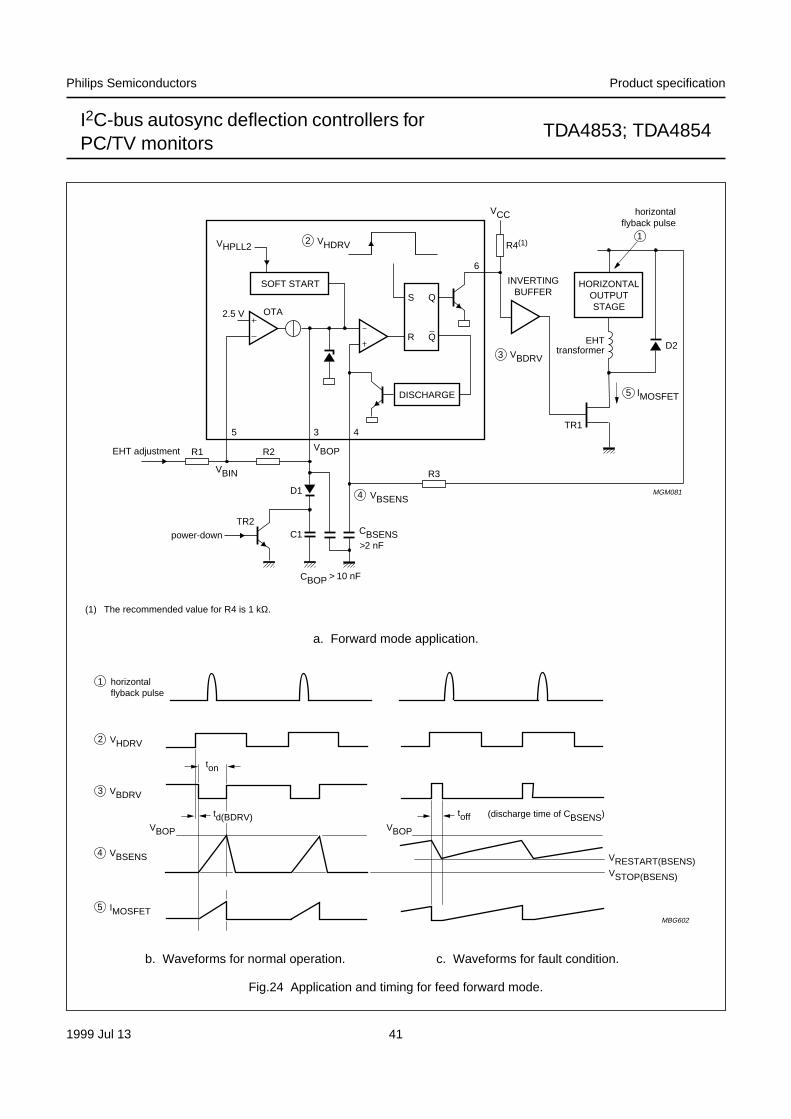
1999 Jul 13 41
Philips Semiconductors Product specification
I2C-bus autosync deflection controllers forPC/TV monitors
TDA4853; TDA4854
Fig.24 Application and timing for feed forward mode.
a. Forward mode application.
b. Waveforms for normal operation. c. Waveforms for fault condition.
handbook, full pagewidth
VBOP VBOP
VSTOP(BSENS)
toff
VRESTART(BSENS)
VHDRV
VBSENS
VBDRV
horizontalflyback pulse
2
3
4
IMOSFET5
1
ton
(discharge time of CBSENS)
MBG602
td(BDRV)
SOFT START
S
R
Q
Q
VHDRV
VCC
6
R4(1)
OTA2.5 V
VHPLL2
5
VBOP
VBSENS
VBDRV
3 4
INVERTINGBUFFER
3
2
4
DISCHARGE
HORIZONTALOUTPUTSTAGE
D2
TR1
R3VBIN
CBSENS
CBOP
R1 R2
C1
D1
TR2
> 10 nF
>2 nF
horizontalflyback pulse
1
IMOSFET5
EHTtransformer
EHT adjustment
power-down
MGM081
(1) The recommended value for R4 is 1 kΩ.
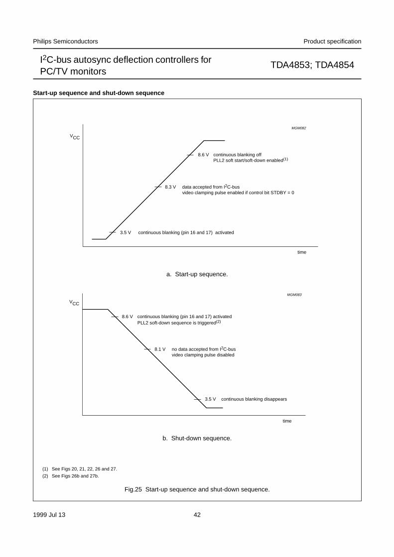
1999 Jul 13 42
Philips Semiconductors Product specification
I2C-bus autosync deflection controllers forPC/TV monitors
TDA4853; TDA4854
Start-up sequence and shut-down sequence
Fig.25 Start-up sequence and shut-down sequence.
a. Start-up sequence.
b. Shut-down sequence.
handbook, full pagewidth
VCC
continuous blanking offPLL2 soft start/soft-down enabled(1)
8.6 V
3.5 V continuous blanking (pin 16 and 17) activated
time
8.3 V data accepted from I2C-busvideo clamping pulse enabled if control bit STDBY = 0
MGM082
handbook, full pagewidth
VCC
MGM083
continuous blanking (pin 16 and 17) activatedPLL2 soft-down sequence is triggered(2)
8.6 V
8.1 V
3.5 V continuous blanking disappears
time
no data accepted from I2C-busvideo clamping pulse disabled
(1) See Figs 20, 21, 22, 26 and 27.
(2) See Figs 26b and 27b.
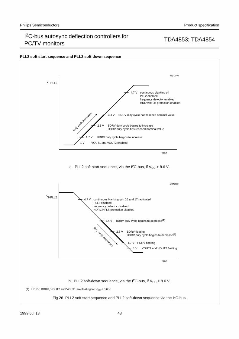
1999 Jul 13 43
Philips Semiconductors Product specification
I2C-bus autosync deflection controllers forPC/TV monitors
TDA4853; TDA4854
PLL2 soft start sequence and PLL2 soft-down sequence
Fig.26 PLL2 soft start sequence and PLL2 soft-down sequence via the I2C-bus.
a. PLL2 soft start sequence, via the I2C-bus, if VCC > 8.6 V.
b. PLL2 soft-down sequence, via the I2C-bus, if VCC > 8.6 V.
(1) HDRV, BDRV, VOUT2 and VOUT1 are floating for VCC < 8.6 V.
handbook, full pagewidth
VHPLL2
continuous blanking offPLL2 enabledfrequency detector enabledHDRV/HFLB protection enabled
4.7 V
3.4 V
1.7 V
time
HDRV duty cycle begins to increase
1 V VOUT1 and VOUT2 enabled
BDRV duty cycle begins to increaseHDRV duty cycle has reached nominal value
2.8 V
BDRV duty cycle has reached nominal value
duty
cycle
incr
ease
s
MGM084
handbook, full pagewidth
VHPLL2continuous blanking (pin 16 and 17) activatedPLL2 disabledfrequency detector disabledHDRV/HFLB protection disabled
4.7 V
3.4 V
1.7 V
time
HDRV floating
1 V VOUT1 and VOUT2 floating
BDRV duty cycle begins to decrease(1)
2.8 V BDRV floatingHDRV duty cycle begins to decrease(1)
duty cycle decreases
MGM085
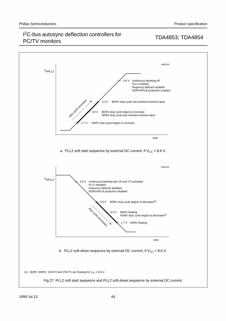
1999 Jul 13 44
Philips Semiconductors Product specification
I2C-bus autosync deflection controllers forPC/TV monitors
TDA4853; TDA4854
Fig.27 PLL2 soft start sequence and PLL2 soft-down sequence by external DC current.
a. PLL2 soft start sequence by external DC current, if VCC > 8.6 V.
b. PLL2 soft-down sequence by external DC current, if VCC > 8.6 V.
(1) HDRV, BDRV, VOUT2 and VOUT1 are floating for VCC < 8.6 V.
handbook, full pagewidth
VHPLL2
continuous blanking offPLL2 enabledfrequency detector enabledHDRV/HFLB protection enabled
4.6 V
3.3 V
1.7 V
time
HDRV duty cycle begins to increase
BDRV duty cycle begins to increaseHDRV duty cycle has reached nominal value
3.0 V
BDRV duty cycle has reached nominal value
duty
cycle
incr
ease
s
MHB108
handbook, full pagewidth
VHPLL2continuous blanking (pin 16 and 17) activatedPLL2 disabledfrequency detector disabledHDRV/HFLB protection disabled
4.6 V
3.3 V
1.7 V
time
HDRV floating
BDRV duty cycle begins to decrease(1)
3.0 V BDRV floatingHDRV duty cycle begins to decrease(1)
duty cycle decreases
MHB109
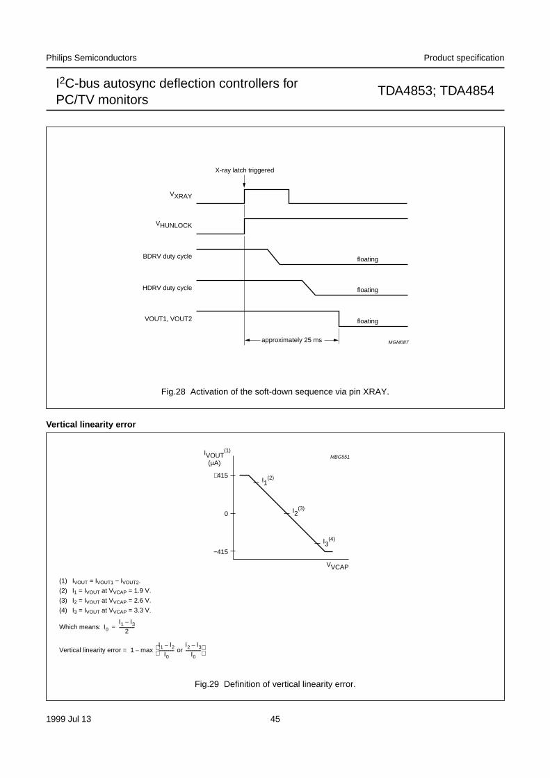
1999 Jul 13 45
Philips Semiconductors Product specification
I2C-bus autosync deflection controllers forPC/TV monitors
TDA4853; TDA4854
handbook, full pagewidth
MGM087
floating
floating
floating
X-ray latch triggered
VXRAY
VHUNLOCK
BDRV duty cycle
HDRV duty cycle
VOUT1, VOUT2
approximately 25 ms
Fig.28 Activation of the soft-down sequence via pin XRAY.
Vertical linearity error
Fig.29 Definition of vertical linearity error.
(1) IVOUT = IVOUT1 − IVOUT2.
(2) I1 = IVOUT at VVCAP = 1.9 V.
(3) I2 = IVOUT at VVCAP = 2.6 V.
(4) I3 = IVOUT at VVCAP = 3.3 V.
Which means:
Vertical linearity error =
I0I1 I3–
2--------------=
1 maxI1 I2–
I0-------------- or
I2 I3–
I0--------------
–
handbook, halfpage
I1(2)
I2(3)
I3(4)
IVOUT(1)
(µA)
+415
−415
0
VVCAP
MBG551
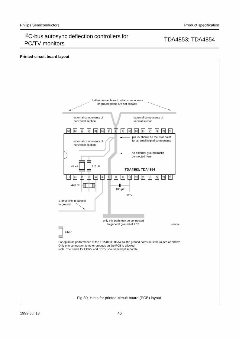
1999 Jul 13 46
Philips Semiconductors Product specification
I2C-bus autosync deflection controllers forPC/TV monitors
TDA4853; TDA4854
Printed-circuit board layout
Fig.30 Hints for printed-circuit board (PCB) layout.
handbook, full pagewidth
TDA4853; TDA4854
1 2 3 5 6 7 8 9 10 11 12 13 14 15 16
32 31 30 29 28 27 26 25 24 23 22 21 20 19 18 17
external components ofhorizontal section
external components ofhorizontal section
B-drive line in parallelto ground
470 pF
2.2 nF47 nF
100 µF
12 V
external components ofvertical section
further connections to other componentsor ground paths are not allowed
only this path may be connectedto general ground of PCB
For optimum performance of the TDA4853; TDA4854 the ground paths must be routed as shown.Only one connection to other grounds on the PCB is allowed.Note: The tracks for HDRV and BDRV should be kept separate.
pin 25 should be the 'star point'for all small signal components
no external ground tracksconnected here
MGM086
SMD
4
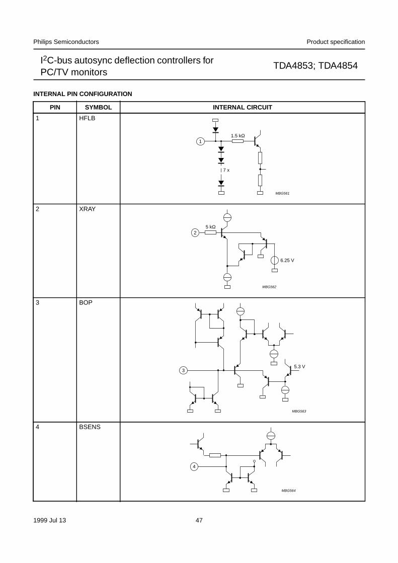
1999 Jul 13 47
Philips Semiconductors Product specification
I2C-bus autosync deflection controllers forPC/TV monitors
TDA4853; TDA4854
INTERNAL PIN CONFIGURATION
PIN SYMBOL INTERNAL CIRCUIT
1 HFLB
2 XRAY
3 BOP
4 BSENS
1.5 kΩ
7 x
1
MBG561
5 kΩ
6.25 V
2
MBG562
5.3 V3
MBG563
4
MBG564
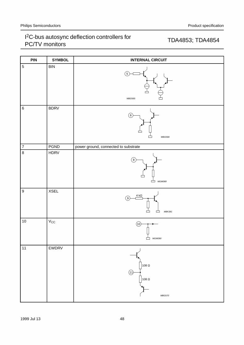
1999 Jul 13 48
Philips Semiconductors Product specification
I2C-bus autosync deflection controllers forPC/TV monitors
TDA4853; TDA4854
5 BIN
6 BDRV
7 PGND power ground, connected to substrate
8 HDRV
9 XSEL
10 VCC
11 EWDRV
PIN SYMBOL INTERNAL CIRCUIT
5
MBG565
6
MBG566
8
MGM089
9
MBK381
4 kΩ
10
MGM090
108 Ω
108 Ω
11
MBG570
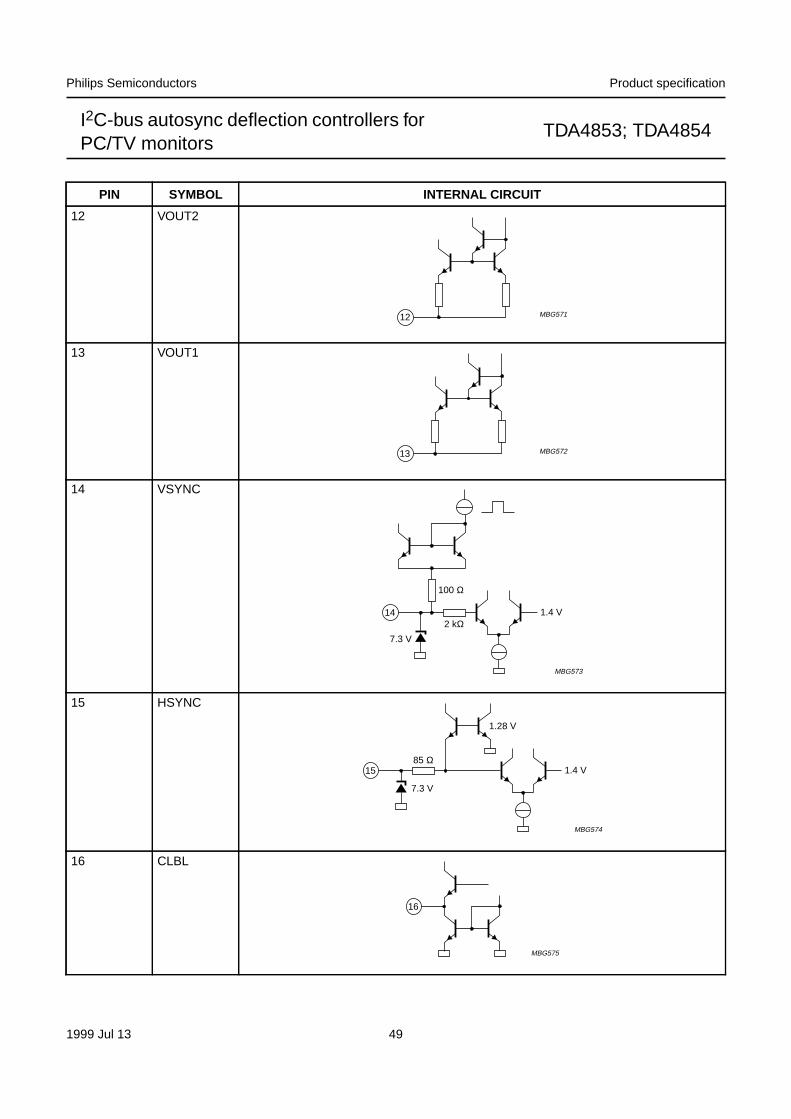
1999 Jul 13 49
Philips Semiconductors Product specification
I2C-bus autosync deflection controllers forPC/TV monitors
TDA4853; TDA4854
12 VOUT2
13 VOUT1
14 VSYNC
15 HSYNC
16 CLBL
PIN SYMBOL INTERNAL CIRCUIT
12 MBG571
13 MBG572
100 Ω
2 kΩ14
7.3 V
1.4 V
MBG573
85 Ω15 1.4 V
1.28 V
7.3 V
MBG574
16
MBG575
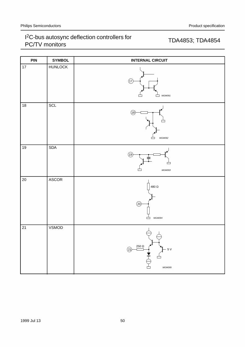
1999 Jul 13 50
Philips Semiconductors Product specification
I2C-bus autosync deflection controllers forPC/TV monitors
TDA4853; TDA4854
17 HUNLOCK
18 SCL
19 SDA
20 ASCOR
21 VSMOD
PIN SYMBOL INTERNAL CIRCUIT
17
MGM091
18
MGM092
19
MGM093
20
480 Ω
MGM094
21250 Ω
5 V
MGM095
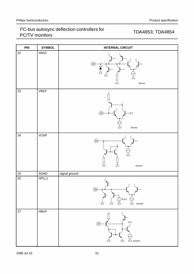
1999 Jul 13 51
Philips Semiconductors Product specification
I2C-bus autosync deflection controllers forPC/TV monitors
TDA4853; TDA4854
22 VAGC
23 VREF
24 VCAP
25 SGND signal ground
26 HPLL1
27 HBUF
PIN SYMBOL INTERNAL CIRCUIT
22
MBG581
23 3 V
MBG582
24
MBG583
26
4.3 V
MGM096
27
MGM097
5 V
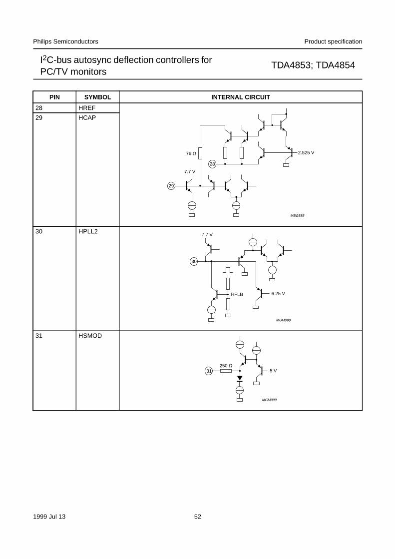
1999 Jul 13 52
Philips Semiconductors Product specification
I2C-bus autosync deflection controllers forPC/TV monitors
TDA4853; TDA4854
28 HREF
29 HCAP
30 HPLL2
31 HSMOD
PIN SYMBOL INTERNAL CIRCUIT
76 Ω
28
2.525 V
29
7.7 V
MBG585
30
7.7 V
6.25 VHFLB
MGM098
31250 Ω
5 V
MGM099
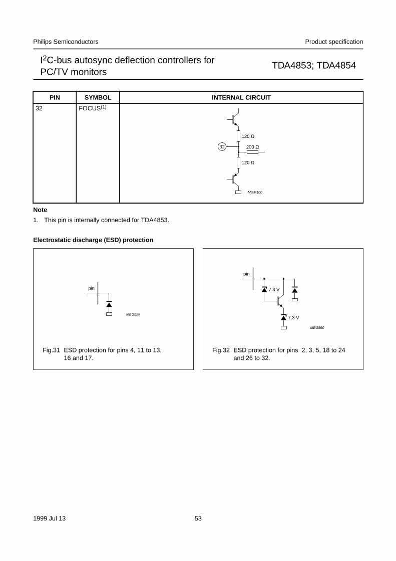
1999 Jul 13 53
Philips Semiconductors Product specification
I2C-bus autosync deflection controllers forPC/TV monitors
TDA4853; TDA4854
Note
1. This pin is internally connected for TDA4853.
32 FOCUS(1)
PIN SYMBOL INTERNAL CIRCUIT
32 200 Ω
120 Ω
120 Ω
MGM100
Electrostatic discharge (ESD) protection
Fig.31 ESD protection for pins 4, 11 to 13,16 and 17.
pin
MBG559
Fig.32 ESD protection for pins 2, 3, 5, 18 to 24and 26 to 32.
pin
7.3 V
7.3 V
MBG560
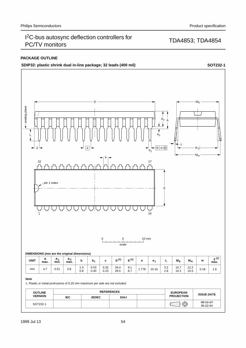
1999 Jul 13 54
Philips Semiconductors Product specification
I2C-bus autosync deflection controllers forPC/TV monitors
TDA4853; TDA4854
PACKAGE OUTLINE
UNIT b1 c E e MHL
REFERENCESOUTLINEVERSION
EUROPEANPROJECTION ISSUE DATE
IEC JEDEC EIAJ
mm
DIMENSIONS (mm are the original dimensions)
SOT232-192-11-1795-02-04
b max.wMEe1
1.30.8
0.530.40
0.320.23
29.428.5
9.18.7
3.22.8 0.181.778 10.16
10.710.2
12.210.5 1.64.7 0.51 3.8
MH
c(e )1
ME
A
L
seat
ing
plan
e
A1
w Mb1
e
D
A2
Z
32
1
17
16
b
E
pin 1 index
0 5 10 mm
scale
Note
1. Plastic or metal protrusions of 0.25 mm maximum per side are not included.
(1) (1)D(1)ZA
max.1 2A
min.A
max.
SDIP32: plastic shrink dual in-line package; 32 leads (400 mil) SOT232-1
1999 Jul 13 55
Philips Semiconductors Product specification
I2C-bus autosync deflection controllers forPC/TV monitors
TDA4853; TDA4854
SOLDERING
Introduction to soldering through-hole mountpackages
This text gives a brief insight to wave, dip and manualsoldering. A more in-depth account of soldering ICs can befound in our “Data Handbook IC26; Integrated CircuitPackages” (document order number 9398 652 90011).
Wave soldering is the preferred method for mounting ofthrough-hole mount IC packages on a printed-circuitboard.
Soldering by dipping or by solder wave
The maximum permissible temperature of the solder is260 °C; solder at this temperature must not be in contactwith the joints for more than 5 seconds.
The total contact time of successive solder waves must notexceed 5 seconds.
The device may be mounted up to the seating plane, butthe temperature of the plastic body must not exceed thespecified maximum storage temperature (Tstg(max)). If theprinted-circuit board has been pre-heated, forced coolingmay be necessary immediately after soldering to keep thetemperature within the permissible limit.
Manual soldering
Apply the soldering iron (24 V or less) to the lead(s) of thepackage, either below the seating plane or not more than2 mm above it. If the temperature of the soldering iron bitis less than 300 °C it may remain in contact for up to10 seconds. If the bit temperature is between300 and 400 °C, contact may be up to 5 seconds.
Suitability of through-hole mount IC packages for dipping and wave soldering methods
Note
1. For SDIP packages, the longitudinal axis must be parallel to the transport direction of the printed-circuit board.
PACKAGESOLDERING METHOD
DIPPING WAVE
DBS, DIP, HDIP, SDIP, SIL suitable suitable(1)
1999 Jul 13 56
Philips Semiconductors Product specification
I2C-bus autosync deflection controllers forPC/TV monitors
TDA4853; TDA4854
DEFINITIONS
LIFE SUPPORT APPLICATIONS
These products are not designed for use in life support appliances, devices, or systems where malfunction of theseproducts can reasonably be expected to result in personal injury. Philips customers using or selling these products foruse in such applications do so at their own risk and agree to fully indemnify Philips for any damages resulting from suchimproper use or sale.
PURCHASE OF PHILIPS I2C COMPONENTS
Data sheet status
Objective specification This data sheet contains target or goal specifications for product development.Preliminary specification This data sheet contains preliminary data; supplementary data may be published later.Product specification This data sheet contains final product specifications.
Limiting values
Limiting values given are in accordance with the Absolute Maximum Rating System (IEC 134). Stress above one ormore of the limiting values may cause permanent damage to the device. These are stress ratings only and operationof the device at these or at any other conditions above those given in the Characteristics sections of the specificationis not implied. Exposure to limiting values for extended periods may affect device reliability.
Application information
Where application information is given, it is advisory and does not form part of the specification.
Purchase of Philips I2C components conveys a license under the Philips’ I2C patent to use thecomponents in the I2C system provided the system conforms to the I2C specification defined byPhilips. This specification can be ordered using the code 9398 393 40011.

1999 Jul 13 57
Philips Semiconductors Product specification
I2C-bus autosync deflection controllers forPC/TV monitors
TDA4853; TDA4854
NOTES

1999 Jul 13 58
Philips Semiconductors Product specification
I2C-bus autosync deflection controllers forPC/TV monitors
TDA4853; TDA4854
NOTES

1999 Jul 13 59
Philips Semiconductors Product specification
I2C-bus autosync deflection controllers forPC/TV monitors
TDA4853; TDA4854
NOTES

© Philips Electronics N.V. SCA
All rights are reserved. Reproduction in whole or in part is prohibited without the prior written consent of the copyright owner.
The information presented in this document does not form part of any quotation or contract, is believed to be accurate and reliable and may be changedwithout notice. No liability will be accepted by the publisher for any consequence of its use. Publication thereof does not convey nor imply any licenseunder patent- or other industrial or intellectual property rights.
Internet: http://www.semiconductors.philips.com
1999 67
Philips Semiconductors – a worldwide company
For all other countries apply to: Philips Semiconductors,International Marketing & Sales Communications, Building BE-p, P.O. Box 218,5600 MD EINDHOVEN, The Netherlands, Fax. +31 40 27 24825
Argentina: see South America
Australia: 3 Figtree Drive, HOMEBUSH, NSW 2140,Tel. +61 2 9704 8141, Fax. +61 2 9704 8139
Austria: Computerstr. 6, A-1101 WIEN, P.O. Box 213,Tel. +43 1 60 101 1248, Fax. +43 1 60 101 1210
Belarus: Hotel Minsk Business Center, Bld. 3, r. 1211, Volodarski Str. 6,220050 MINSK, Tel. +375 172 20 0733, Fax. +375 172 20 0773
Belgium: see The Netherlands
Brazil: see South America
Bulgaria: Philips Bulgaria Ltd., Energoproject, 15th floor,51 James Bourchier Blvd., 1407 SOFIA,Tel. +359 2 68 9211, Fax. +359 2 68 9102
Canada: PHILIPS SEMICONDUCTORS/COMPONENTS,Tel. +1 800 234 7381, Fax. +1 800 943 0087
China/Hong Kong: 501 Hong Kong Industrial Technology Centre,72 Tat Chee Avenue, Kowloon Tong, HONG KONG,Tel. +852 2319 7888, Fax. +852 2319 7700
Colombia: see South America
Czech Republic: see Austria
Denmark: Sydhavnsgade 23, 1780 COPENHAGEN V,Tel. +45 33 29 3333, Fax. +45 33 29 3905
Finland: Sinikalliontie 3, FIN-02630 ESPOO,Tel. +358 9 615 800, Fax. +358 9 6158 0920
France: 51 Rue Carnot, BP317, 92156 SURESNES Cedex,Tel. +33 1 4099 6161, Fax. +33 1 4099 6427
Germany: Hammerbrookstraße 69, D-20097 HAMBURG,Tel. +49 40 2353 60, Fax. +49 40 2353 6300
Hungary: see Austria
India: Philips INDIA Ltd, Band Box Building, 2nd floor,254-D, Dr. Annie Besant Road, Worli, MUMBAI 400 025,Tel. +91 22 493 8541, Fax. +91 22 493 0966
Indonesia: PT Philips Development Corporation, Semiconductors Division,Gedung Philips, Jl. Buncit Raya Kav.99-100, JAKARTA 12510,Tel. +62 21 794 0040 ext. 2501, Fax. +62 21 794 0080
Ireland: Newstead, Clonskeagh, DUBLIN 14,Tel. +353 1 7640 000, Fax. +353 1 7640 200
Israel: RAPAC Electronics, 7 Kehilat Saloniki St, PO Box 18053,TEL AVIV 61180, Tel. +972 3 645 0444, Fax. +972 3 649 1007
Italy: PHILIPS SEMICONDUCTORS, Via Casati, 23 - 20052 MONZA (MI),Tel. +39 039 203 6838, Fax +39 039 203 6800
Japan: Philips Bldg 13-37, Kohnan 2-chome, Minato-ku,TOKYO 108-8507, Tel. +81 3 3740 5130, Fax. +81 3 3740 5057
Korea: Philips House, 260-199 Itaewon-dong, Yongsan-ku, SEOUL,Tel. +82 2 709 1412, Fax. +82 2 709 1415
Malaysia: No. 76 Jalan Universiti, 46200 PETALING JAYA, SELANGOR,Tel. +60 3 750 5214, Fax. +60 3 757 4880
Mexico: 5900 Gateway East, Suite 200, EL PASO, TEXAS 79905,Tel. +9-5 800 234 7381, Fax +9-5 800 943 0087
Middle East: see Italy
Netherlands: Postbus 90050, 5600 PB EINDHOVEN, Bldg. VB,Tel. +31 40 27 82785, Fax. +31 40 27 88399
New Zealand: 2 Wagener Place, C.P.O. Box 1041, AUCKLAND,Tel. +64 9 849 4160, Fax. +64 9 849 7811
Norway: Box 1, Manglerud 0612, OSLO,Tel. +47 22 74 8000, Fax. +47 22 74 8341
Pakistan: see Singapore
Philippines: Philips Semiconductors Philippines Inc.,106 Valero St. Salcedo Village, P.O. Box 2108 MCC, MAKATI,Metro MANILA, Tel. +63 2 816 6380, Fax. +63 2 817 3474
Poland: Ul. Lukiska 10, PL 04-123 WARSZAWA,Tel. +48 22 612 2831, Fax. +48 22 612 2327
Portugal: see Spain
Romania: see Italy
Russia: Philips Russia, Ul. Usatcheva 35A, 119048 MOSCOW,Tel. +7 095 755 6918, Fax. +7 095 755 6919
Singapore: Lorong 1, Toa Payoh, SINGAPORE 319762,Tel. +65 350 2538, Fax. +65 251 6500
Slovakia: see Austria
Slovenia: see Italy
South Africa: S.A. PHILIPS Pty Ltd., 195-215 Main Road Martindale,2092 JOHANNESBURG, P.O. Box 58088 Newville 2114,Tel. +27 11 471 5401, Fax. +27 11 471 5398
South America: Al. Vicente Pinzon, 173, 6th floor,04547-130 SÃO PAULO, SP, Brazil,Tel. +55 11 821 2333, Fax. +55 11 821 2382
Spain: Balmes 22, 08007 BARCELONA,Tel. +34 93 301 6312, Fax. +34 93 301 4107
Sweden: Kottbygatan 7, Akalla, S-16485 STOCKHOLM,Tel. +46 8 5985 2000, Fax. +46 8 5985 2745
Switzerland: Allmendstrasse 140, CH-8027 ZÜRICH,Tel. +41 1 488 2741 Fax. +41 1 488 3263
Taiwan: Philips Semiconductors, 6F, No. 96, Chien Kuo N. Rd., Sec. 1,TAIPEI, Taiwan Tel. +886 2 2134 2886, Fax. +886 2 2134 2874
Thailand: PHILIPS ELECTRONICS (THAILAND) Ltd.,209/2 Sanpavuth-Bangna Road Prakanong, BANGKOK 10260,Tel. +66 2 745 4090, Fax. +66 2 398 0793
Turkey: Yukari Dudullu, Org. San. Blg., 2.Cad. Nr. 28 81260 Umraniye,ISTANBUL, Tel. +90 216 522 1500, Fax. +90 216 522 1813
Ukraine : PHILIPS UKRAINE, 4 Patrice Lumumba str., Building B, Floor 7,252042 KIEV, Tel. +380 44 264 2776, Fax. +380 44 268 0461
United Kingdom: Philips Semiconductors Ltd., 276 Bath Road, Hayes,MIDDLESEX UB3 5BX, Tel. +44 208 730 5000, Fax. +44 208 754 8421
United States: 811 East Arques Avenue, SUNNYVALE, CA 94088-3409,Tel. +1 800 234 7381, Fax. +1 800 943 0087
Uruguay: see South America
Vietnam: see Singapore
Yugoslavia: PHILIPS, Trg N. Pasica 5/v, 11000 BEOGRAD,Tel. +381 11 62 5344, Fax.+381 11 63 5777
Printed in The Netherlands 545004/02/pp60 Date of release: 1999 Jul 13 Document order number: 9397 750 05275

This datasheet has been download from:
www.datasheetcatalog.com
Datasheets for electronics components.