Embed Size (px)
Citation preview
DATA SHEET
Product specificationSupersedes data of 2004 Oct 21
2004 Nov 12
INTEGRATED CIRCUITS
TEA6848HNew In Car Entertainment car radiotuner IC with Precision AdjacentChannel Suppression(NICE-PACS)
2004 Nov 12 2
Philips Semiconductors Product specification
New In Car Entertainment car radio tuner IC withPrecision Adjacent Channel Suppression (NICE-PACS)
TEA6848H
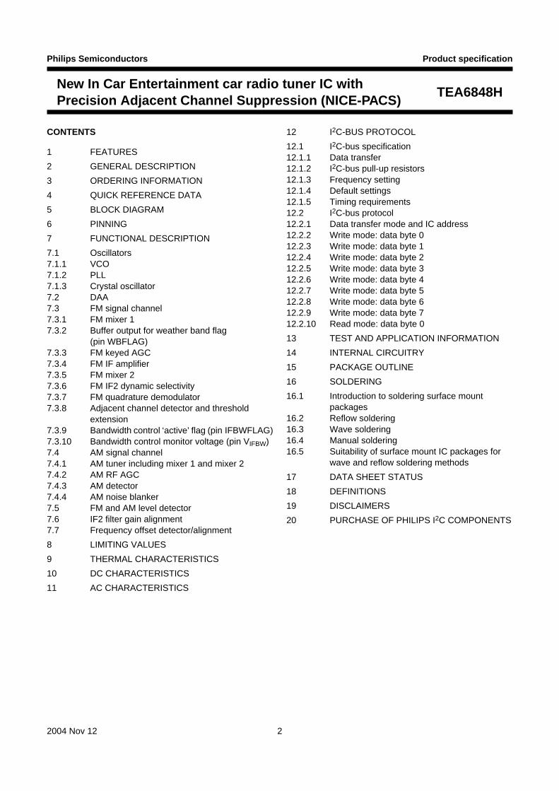
CONTENTS
1 FEATURES
2 GENERAL DESCRIPTION
3 ORDERING INFORMATION
4 QUICK REFERENCE DATA
5 BLOCK DIAGRAM
6 PINNING
7 FUNCTIONAL DESCRIPTION
7.1 Oscillators7.1.1 VCO7.1.2 PLL7.1.3 Crystal oscillator7.2 DAA7.3 FM signal channel7.3.1 FM mixer 17.3.2 Buffer output for weather band flag
(pin WBFLAG)7.3.3 FM keyed AGC7.3.4 FM IF amplifier7.3.5 FM mixer 27.3.6 FM IF2 dynamic selectivity7.3.7 FM quadrature demodulator7.3.8 Adjacent channel detector and threshold
extension7.3.9 Bandwidth control ‘active’ flag (pin IFBWFLAG)7.3.10 Bandwidth control monitor voltage (pin VIFBW)7.4 AM signal channel7.4.1 AM tuner including mixer 1 and mixer 27.4.2 AM RF AGC7.4.3 AM detector7.4.4 AM noise blanker7.5 FM and AM level detector7.6 IF2 filter gain alignment7.7 Frequency offset detector/alignment
8 LIMITING VALUES
9 THERMAL CHARACTERISTICS
10 DC CHARACTERISTICS
11 AC CHARACTERISTICS
12 I2C-BUS PROTOCOL
12.1 I2C-bus specification12.1.1 Data transfer12.1.2 I2C-bus pull-up resistors12.1.3 Frequency setting12.1.4 Default settings12.1.5 Timing requirements12.2 I2C-bus protocol12.2.1 Data transfer mode and IC address12.2.2 Write mode: data byte 012.2.3 Write mode: data byte 112.2.4 Write mode: data byte 212.2.5 Write mode: data byte 312.2.6 Write mode: data byte 412.2.7 Write mode: data byte 512.2.8 Write mode: data byte 612.2.9 Write mode: data byte 712.2.10 Read mode: data byte 0
13 TEST AND APPLICATION INFORMATION
14 INTERNAL CIRCUITRY
15 PACKAGE OUTLINE
16 SOLDERING
16.1 Introduction to soldering surface mountpackages
16.2 Reflow soldering16.3 Wave soldering16.4 Manual soldering16.5 Suitability of surface mount IC packages for
wave and reflow soldering methods
17 DATA SHEET STATUS
18 DEFINITIONS
19 DISCLAIMERS
20 PURCHASE OF PHILIPS I2C COMPONENTS
2004 Nov 12 3
Philips Semiconductors Product specification
New In Car Entertainment car radio tuner IC withPrecision Adjacent Channel Suppression (NICE-PACS)
TEA6848H
1 FEATURES
• FM mixer 1 for conversion of FM RF (65 to 108 MHzand US weather band) to IF of 10.7 MHz; the mixerprovides inherent image rejection; for European andUS FM band/WB (weather band) the mixer is driven witha ‘high’ injection Local Oscillator (LO); in JapanFM band and East Europe FM band the mixer is drivenwith a ‘low’ injection LO
• AM mixer 1 for conversion of AM RF to AM IF1 of10.7 MHz
• LC tuner oscillator providing mixer frequencies forFM mixer and AM mixer 1
• AM mixer 2 for conversion of AM IF1 to AM IF2 of450 kHz
• Crystal oscillator providing mixer frequencies forAM mixer 2 and FM mixer 2 and reference forsynthesizer PLL, IF count, timing for Radio Data System(RDS) update and reference frequency for car audiosignal processor ICs
• Fast synthesizer PLL tuning system with local control forinaudible RDS updating
• Timing function for RDS update algorithm and controlsignal output for car audio signal processor ICs(TEA688x, SAA77xx, TEF689x)
• Digital alignment circuit for bus controlled matching ofoscillator tuning voltage to FM antenna tank circuittuning voltage
• AGC PIN diode drive circuit for FM RF AGC; AGCdetection at FM mixer input; the AGC PIN diode drivecan be activated by the I2C-bus as a local function forsearch tuning; AGC threshold is a programmable andkeyed function switchable via the I2C-bus
• FM IF linear amplifier with high dynamic input range
• FM mixer 2 for conversion of FM IF1 to FM IF2 of450 kHz with inherent image rejection
• Fully integrated dynamic selectivity andFM demodulator at IF2; improved sensitivity withdynamic threshold extension; centre frequency of IF2selectivity alignment via the I2C-bus
• Level detector for AM and FM with temperaturecompensated output voltage; starting point and slope oflevel output is programmable via the I2C-bus
• AM cascode AGC stage and RF PIN diode drive circuit;AGC threshold detection at AM mixer 1 and IF2 AGCinput; threshold for detection at mixer 1 input isprogrammable via the I2C-bus
• AM IF2 AGC and demodulator
• AM AF output switchable to provide AM IF2 forAM stereo decoder
• AM noise blanker with detection at IF1 and blanking atAM IF2
• Software controlled flag output
• Buffer output for weather band flag
• Adjacent channel detector, modulation detector andfrequency offset for instantaneous bandwidth control ofthe integrated filter
• Flag and voltage output indicating the actual bandwidth
• I2C-bus alignment of centre frequency and gain variationas functions of bandwidth of the IF2 filter and centrefrequency of the offset detector.
2 GENERAL DESCRIPTION
The TEA6848H is a single IC with car radio tuner for AM,FM and Weather Band (WB) intended for microcontrollertuning with the I2C-bus. It provides the following functions:
• AM double conversion receiver for LW, MW and SW(31 m, 41 m and 49 m bands) with IF1 = 10.7 MHz andIF2 = 450 kHz
• FM double conversion receiver with integrated imagerejection for IF1 and for IF2 capable of selecting US FM,US weather, Europe FM, East Europe FM andJapan FM bands; fully integrated dynamic selectivity at450 kHz FM IF2; FM demodulator with dynamicthreshold extension; centre frequency alignment of IF2selectivity via the I2C-bus
• The tuning system includes VCO, crystal oscillator andPLL synthesizer on one chip.
3 ORDERING INFORMATION
TYPE NUMBERPACKAGE
NAME DESCRIPTION VERSION
TEA6848H LQFP80 plastic low profile quad flat package; 80 leads; body 12 × 12 × 1.4 mm SOT315-1
2004 Nov 12 4
Philips Semiconductors Product specification
New In Car Entertainment car radio tuner IC withPrecision Adjacent Channel Suppression (NICE-PACS)
TEA6848H
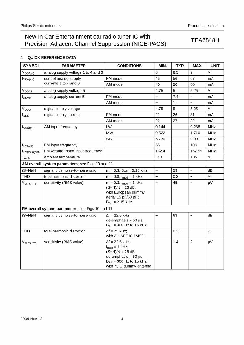
4 QUICK REFERENCE DATA
SYMBOL PARAMETER CONDITIONS MIN. TYP. MAX. UNIT
VDDA(n) analog supply voltage 1 to 4 and 6 8 8.5 9 V
IDDA(tot) sum of analog supplycurrents 1 to 4 and 6
FM mode 45 56 67 mA
AM mode 40 50 60 mA
VDDA5 analog supply voltage 5 4.75 5 5.25 V
IDDA5 analog supply current 5 FM mode − 7.4 − mA
AM mode − 11 − mA
VDDD digital supply voltage 4.75 5 5.25 V
IDDD digital supply current FM mode 21 26 31 mA
AM mode 22 27 32 mA
fAM(ant) AM input frequency LW 0.144 − 0.288 MHz
MW 0.522 − 1.710 MHz
SW 5.730 − 9.99 MHz
fFM(ant) FM input frequency 65 − 108 MHz
fFM(WB)(ant) FM weather band input frequency 162.4 − 162.55 MHz
Tamb ambient temperature −40 − +85 °C
AM overall system parameters ; see Figs 10 and 11
(S+N)/N signal plus noise-to-noise ratio m = 0.3; BAF = 2.15 kHz − 59 − dB
THD total harmonic distortion m = 0.8; fmod = 1 kHz − 0.3 − %
Vsens(rms) sensitivity (RMS value) m = 0.3; fmod = 1 kHz;(S+N)/N = 26 dB;with European dummyaerial 15 pF/60 pF;BAF = 2.15 kHz
− 45 − µV
FM overall system parameters ; see Figs 10 and 11
(S+N)/N signal plus noise-to-noise ratio ∆f = 22.5 kHz;de-emphasis = 50 µs;BAF = 300 Hz to 15 kHz
− 63 − dB
THD total harmonic distortion ∆f = 75 kHz;with 2 × SFE10.7MS3
− 0.35 − %
Vsens(rms) sensitivity (RMS value) ∆f = 22.5 kHz;fmod = 1 kHz;(S+N)/N = 26 dB;de-emphasis = 50 µs;BAF = 300 Hz to 15 kHz;with 75 Ω dummy antenna
− 1.4 2 µV
2004N
ov12
5
Philips S
emiconductors
Product specification
New
In Car E
ntertainment car radio tuner IC
with
Precision
AdjacentC
hannelSuppression
(NIC
E-PA
CS
)T
EA
6848H
This text is here in white to force landscape pages to be rotated correctly when browsing through the pdf in the Acrobat reader.This text is here in_white to force landscape pages to be rotated correctly when browsing through the pdf in the Acrobat reader.This text is here inThis text is here inwhite to force landscape pages to be rotated correctly when browsing through the pdf in the Acrobat reader. white to force landscape pages to be ...
5B
LOC
K D
IAG
RA
M
hand
book
, ful
l pag
ewid
th
DAA
RDSUPDATE
CRYSTALOSCILLATOR
POWERSUPPLYVCO
AMMIXER 1
AMMIXER 2
AM
AGC
90°
FMI/Q MIXER 1
FMAGC
TUNING SYSTEM
AM NOISEDETECTOR
PEAK/AVERAGE
BLANKPULSE
LEVELDAA
÷10/÷20
÷1/ ÷2/÷3
90°
IFCOUNT
TEA6848H
AMDEMOD
FMMIXER 2
÷2
MUX
IFFILTER
FMDEMOD
STABI
BUFFER
BANDWIDTHCONTROL
x1/ x15AMPLIFIER
MPXOUT
19 18 15 14 13 12 11 10 9 8 7 6 5 4 3 2 120
22
23
24
25
26
2728
29
303132
3334
35
36
37
38
39
40DAAIN
DAATD
DAAOUT
TKEYEDAGC
TFMAGC
IFMAGC
WBFLAG
FMMIXIN2
FMMIXIN1
Vref(MIX)
i.c.RFGND
IAMAGC
VAMCAS
VAMCASFB
AMMIX1IN
AMMIX1DEC
SWFLAG
VDDA2
MIX1OUT2
MIX1OUT1
FMLIMDCFDB1AMIF2DECAMNBHOLD
IFAMPOUT
IFCDAATEST
FMMIX2DEC
COFFSET
FMMIX2IN
IF1GND
AMIF2IN
VDDA1IFAMPIN
IFAMPDEC
IF2FILQ
IF2FILI
FMLIMDCFDB2IREFFMIF2
THFAMAGC
TAFAMAGC
41 42 43 44 45 46 47 48 49 50 5251 53 54 55 56 57 58 59 60
MODDETVDDA5FMMPXRDSMPXAMAFIF2
TRDSMUTE
AFHOLD
AFSAMPLE
MPXDCFDB
VDDA4
OSCTNK
OSCFDB
VCOGND
DGNDVDDD
FREFVDDA3
CPOUTVtunei.c.
61VDDA6
IFBWFLAG
SDA
SCL
VIFBWIF2GND
CINT
MODETOUT
TACDVlevel(AMFM)
XTAL1
XTALGND
XTAL2
Vlevel(ACD)
ACDTHRES
IREFAMMIX2OUT1
AMMIX2OUT2
CAGCVref(lim)
62
63
64
65
66
67
68
69
70
71
72
73
74
75
76
77
78
7980
AM
LEVEL
LEVEL
WB
LEVEL
20.5 MHz
FM AMWB/JAPAN/OIRT
21
17 16
ANTENNA
AM STEREO
MUTERDS
I2C-bus
I2C-bus
I2C-bus
I2C-bus
I2C-bus
I2C-bus
I2C-BUS
I2C-bus
MHC436
×
×
×
×
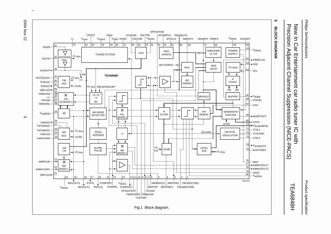
Fig.1 Block diagram.
2004 Nov 12 6
Philips Semiconductors Product specification
New In Car Entertainment car radio tuner IC withPrecision Adjacent Channel Suppression (NICE-PACS)
TEA6848H
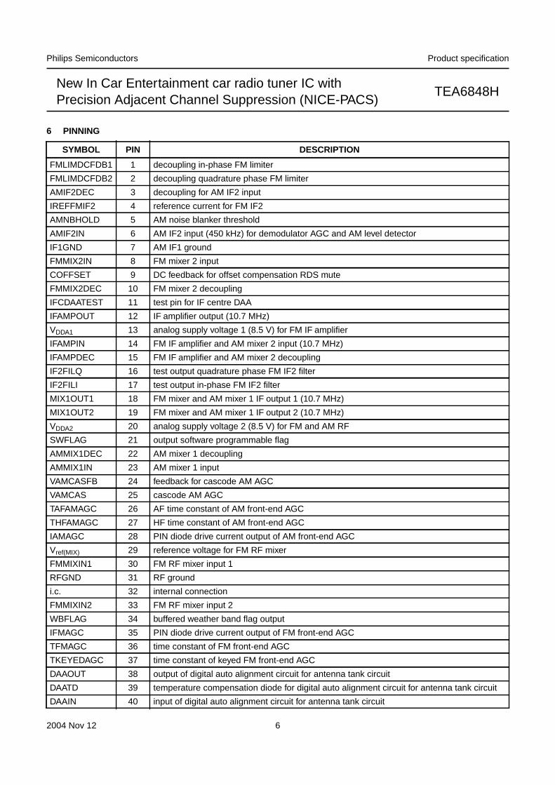
6 PINNING
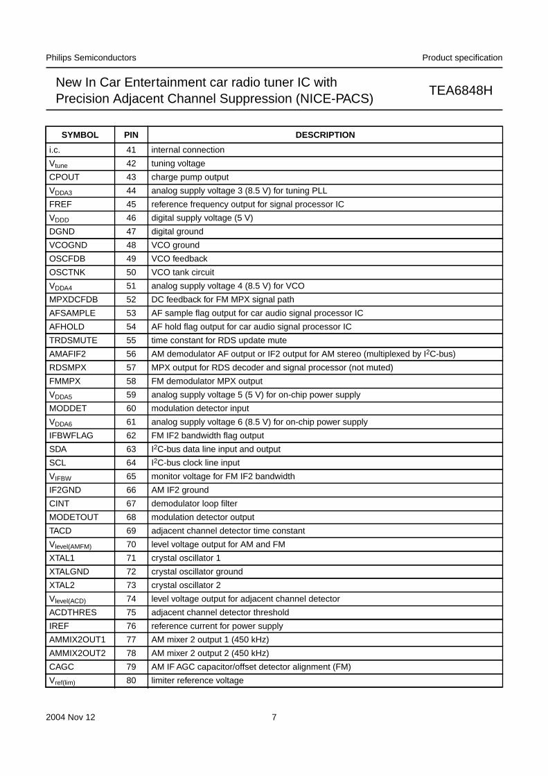
SYMBOL PIN DESCRIPTION
FMLIMDCFDB1 1 decoupling in-phase FM limiter
FMLIMDCFDB2 2 decoupling quadrature phase FM limiter
AMIF2DEC 3 decoupling for AM IF2 input
IREFFMIF2 4 reference current for FM IF2
AMNBHOLD 5 AM noise blanker threshold
AMIF2IN 6 AM IF2 input (450 kHz) for demodulator AGC and AM level detector
IF1GND 7 AM IF1 ground
FMMIX2IN 8 FM mixer 2 input
COFFSET 9 DC feedback for offset compensation RDS mute
FMMIX2DEC 10 FM mixer 2 decoupling
IFCDAATEST 11 test pin for IF centre DAA
IFAMPOUT 12 IF amplifier output (10.7 MHz)
VDDA1 13 analog supply voltage 1 (8.5 V) for FM IF amplifier
IFAMPIN 14 FM IF amplifier and AM mixer 2 input (10.7 MHz)
IFAMPDEC 15 FM IF amplifier and AM mixer 2 decoupling
IF2FILQ 16 test output quadrature phase FM IF2 filter
IF2FILI 17 test output in-phase FM IF2 filter
MIX1OUT1 18 FM mixer and AM mixer 1 IF output 1 (10.7 MHz)
MIX1OUT2 19 FM mixer and AM mixer 1 IF output 2 (10.7 MHz)
VDDA2 20 analog supply voltage 2 (8.5 V) for FM and AM RF
SWFLAG 21 output software programmable flag
AMMIX1DEC 22 AM mixer 1 decoupling
AMMIX1IN 23 AM mixer 1 input
VAMCASFB 24 feedback for cascode AM AGC
VAMCAS 25 cascode AM AGC
TAFAMAGC 26 AF time constant of AM front-end AGC
THFAMAGC 27 HF time constant of AM front-end AGC
IAMAGC 28 PIN diode drive current output of AM front-end AGC
Vref(MIX) 29 reference voltage for FM RF mixer
FMMIXIN1 30 FM RF mixer input 1
RFGND 31 RF ground
i.c. 32 internal connection
FMMIXIN2 33 FM RF mixer input 2
WBFLAG 34 buffered weather band flag output
IFMAGC 35 PIN diode drive current output of FM front-end AGC
TFMAGC 36 time constant of FM front-end AGC
TKEYEDAGC 37 time constant of keyed FM front-end AGC
DAAOUT 38 output of digital auto alignment circuit for antenna tank circuit
DAATD 39 temperature compensation diode for digital auto alignment circuit for antenna tank circuit
DAAIN 40 input of digital auto alignment circuit for antenna tank circuit
2004 Nov 12 7
Philips Semiconductors Product specification
New In Car Entertainment car radio tuner IC withPrecision Adjacent Channel Suppression (NICE-PACS)
TEA6848H
i.c. 41 internal connection
Vtune 42 tuning voltage
CPOUT 43 charge pump output
VDDA3 44 analog supply voltage 3 (8.5 V) for tuning PLL
FREF 45 reference frequency output for signal processor IC
VDDD 46 digital supply voltage (5 V)
DGND 47 digital ground
VCOGND 48 VCO ground
OSCFDB 49 VCO feedback
OSCTNK 50 VCO tank circuit
VDDA4 51 analog supply voltage 4 (8.5 V) for VCO
MPXDCFDB 52 DC feedback for FM MPX signal path
AFSAMPLE 53 AF sample flag output for car audio signal processor IC
AFHOLD 54 AF hold flag output for car audio signal processor IC
TRDSMUTE 55 time constant for RDS update mute
AMAFIF2 56 AM demodulator AF output or IF2 output for AM stereo (multiplexed by I2C-bus)
RDSMPX 57 MPX output for RDS decoder and signal processor (not muted)
FMMPX 58 FM demodulator MPX output
VDDA5 59 analog supply voltage 5 (5 V) for on-chip power supply
MODDET 60 modulation detector input
VDDA6 61 analog supply voltage 6 (8.5 V) for on-chip power supply
IFBWFLAG 62 FM IF2 bandwidth flag output
SDA 63 I2C-bus data line input and output
SCL 64 I2C-bus clock line input
VIFBW 65 monitor voltage for FM IF2 bandwidth
IF2GND 66 AM IF2 ground
CINT 67 demodulator loop filter
MODETOUT 68 modulation detector output
TACD 69 adjacent channel detector time constant
Vlevel(AMFM) 70 level voltage output for AM and FM
XTAL1 71 crystal oscillator 1
XTALGND 72 crystal oscillator ground
XTAL2 73 crystal oscillator 2
Vlevel(ACD) 74 level voltage output for adjacent channel detector
ACDTHRES 75 adjacent channel detector threshold
IREF 76 reference current for power supply
AMMIX2OUT1 77 AM mixer 2 output 1 (450 kHz)
AMMIX2OUT2 78 AM mixer 2 output 2 (450 kHz)
CAGC 79 AM IF AGC capacitor/offset detector alignment (FM)
Vref(lim) 80 limiter reference voltage
SYMBOL PIN DESCRIPTION

2004 Nov 12 8
Philips Semiconductors Product specification
New In Car Entertainment car radio tuner IC withPrecision Adjacent Channel Suppression (NICE-PACS)
TEA6848H
handbook, full pagewidth
TEA6848H
MHC437
1
2
3
4
5
6
7
8
9
10
11
12
13
14
15
16
17
18
19
20
60
59
58
57
56
55
54
53
52
51
50
49
48
47
46
45
44
43
42
41
21 22 23 24 25 26 27 28 29 30 31 32 33 34 35 36 37 38 39 40
80 79 78 77 76 75 74 73 72 71 70 69 68 67 66 65 64 63 62 61
Vre
f(lim
)
CA
GC
AM
MIX
2OU
T2
AM
MIX
2OU
T1
IRE
F
AC
DT
HR
ES
Vle
vel(A
CD
)
XT
AL2
XT
ALG
ND
XT
AL1
Vle
vel(A
MF
M)
TA
CD
MO
DE
TO
UT
CIN
T
IF2G
ND
VIF
BW
SC
L
SD
A
IFB
WF
LAG
VD
DA
6
SW
FLA
G
AM
MIX
1DE
C
AM
MIX
1IN
VA
MC
AS
FB
VA
MC
AS
TA
FA
MA
GC
TH
FA
MA
GC
IAM
AG
C
Vre
f(M
IX)
FM
MIX
IN1
RF
GN
D i.c.
FM
MIX
IN2
WB
FLA
G
IFM
AG
C
TF
MA
GC
TK
EY
ED
AG
C
DA
AO
UT
DA
AT
D
DA
AIN
FMLIMDCFDB1
FMLIMDCFDB2
AMIF2DEC
IREFFMIF2
AMNBHOLD
AMIF2IN
IF1GND
FMMIX2IN
COFFSET
FMMIX2DEC
IFCDAATEST
IFAMPOUT
VDDA1
IFAMPIN
IFAMPDEC
IF2FILQ
IF2FILI
MIX1OUT1
MIX1OUT2
VDDA2
MODDET
VDDA5
FMMPX
RDSMPX
AMAFIF2
TRDSMUTE
AFHOLD
AFSAMPLE
MPXDCFDB
VDDA4
OSCTNK
OSCFDB
VCOGND
DGND
VDDD
FREF
VDDA3
CPOUT
Vtune
i.c.
Fig.2 Pin configuration.

2004 Nov 12 9
Philips Semiconductors Product specification
New In Car Entertainment car radio tuner IC withPrecision Adjacent Channel Suppression (NICE-PACS)
TEA6848H
7 FUNCTIONAL DESCRIPTION
7.1 Oscillators
7.1.1 VCO
The varactor tuned VCO provides the local oscillator signalfor both FM and AM mixer 1. It has a frequency range of162.9 to 248.2 MHz.
7.1.2 PLL
Fast synthesizer PLL tuning system with local control forinaudible RDS updating.
7.1.3 CRYSTAL OSCILLATOR
The crystal oscillator provides a 20.5 MHz signal that isused for:
• Reference frequency for frequency synthesizer PLL
• Local oscillator for AM mixer 2 and FM mixer 2
• Reference frequency for the IF counter
• Timing signal for the RDS update algorithm
• Reference frequency (75.368 kHz) for the TEA688x (caraudio signal processor - CASP) or TEF689x (car radiointegrated signal processor - CRISP).
7.2 DAA
To reduce the number of manual alignments in productionthe following I2C-bus controlled Digital Auto Alignment(DAA) functions are included:
• FM RF DAA
– 7-bit DAA circuitry for the conversion of the VCOtuning voltage to a controlled alignment voltage forthe FM antenna tank circuit
• FM and AM level DAA
– Level DAA circuitry for alignment of slope (3-bit) andstarting point (5-bit) of the level curve
• IF2 centre DAA
– Centre frequency alignment (7-bit) of integratedFM IF2 dynamic selectivity.
7.3 FM signal channel
7.3.1 FM MIXER 1
FM quadrature mixer converts FM RF (65 to 108 MHz andweather band) to IF of 10.7 MHz. The FM mixer providesinherent image rejection and high RF sensitivity.
It is capable of tuning the US FM, US weather,Europe FM, Japan FM and East Europe FM bands:
• US FM = 87.9 to 107.9 MHz
• US weather FM = 162.4 to 162.55 MHz
• Europe FM = 87.5 to 108 MHz
• Japan FM = 76 to 91 MHz
• East Europe FM = 65 to 74 MHz.
7.3.2 BUFFER OUTPUT FOR WEATHER BAND FLAG
(PIN WBFLAG)
The buffer output on pin WBFLAG is HIGH for weatherband mode.
7.3.3 FM KEYED AGC
The AGC threshold is programmable and the keyed AGCfunction is switchable via the I2C-bus. AGC detectionoccurs at the input of the first FM mixer. If the keyed AGCfunction is activated, the AGC is keyed only by the narrowband level. The AGC PIN diode drive can be activated viathe I2C-bus as a local function for search tuning. The AGCsources a constant 10 mA current into the FM PIN diode inAM mode.
7.3.4 FM IF AMPLIFIER
The FM IF amplifier provides 18 dB amplification with highlinearity over a wide dynamic range.
7.3.5 FM MIXER 2
The FM mixer 2 converts 10.7 MHz FM IF1 to 450 kHzFM IF2 in I and Q phase to achieve image rejection in thedemodulator.
2004 Nov 12 10
Philips Semiconductors Product specification
New In Car Entertainment car radio tuner IC withPrecision Adjacent Channel Suppression (NICE-PACS)
TEA6848H
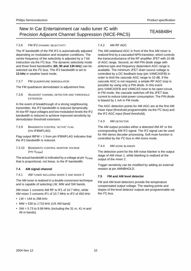
7.3.6 FM IF2 DYNAMIC SELECTIVITY
The IF bandwidth of the FM IF2 is automatically adjusteddepending on modulation and reception conditions. Thecentre frequency of the selectivity is adjusted by a 7-bitinstruction via the I2C-bus. The dynamic selectivity modeand three fixed bandwidths (60, 90 and 130 kHz ) can beselected via the I2C-bus. The IF2 bandwidth is set to13 kHz in weather band mode.
7.3.7 FM QUADRATURE DEMODULATOR
The FM quadrature demodulator is adjustment free.
7.3.8 ADJACENT CHANNEL DETECTOR AND THRESHOLD
EXTENSION
In the event of breakthrough of a strong neighbouringtransmitter, the IF2 bandwidth is reduced dynamically.At low RF input voltages and low modulation levels the IF2bandwidth is reduced to achieve improved sensitivity bydemodulator threshold extension.
7.3.9 BANDWIDTH CONTROL ‘ACTIVE’ FLAG
(PIN IFBWFLAG)
Flag output IBFW = 1 from pin IFBWFLAG indicates thatthe IF2 bandwidth is reduced.
7.3.10 BANDWIDTH CONTROL MONITOR VOLTAGE
(PIN VIFBW)
The actual bandwidth is indicated by a voltage at pin VIFBWthat is proportional, not linear, to the IF bandwidth.
7.4 AM signal channel
7.4.1 AM TUNER INCLUDING MIXER 1 AND MIXER 2
The AM tuner is realized in a double conversion techniqueand is capable of selecting LW, MW and SW bands.
AM mixer 1 converts AM RF to IF1 of 10.7 MHz, whileAM mixer 2 converts IF1 of 10.7 MHz to IF2 of 450 kHz:
• LW = 144 to 288 kHz
• MW = 530 to 1710 kHz (US AM band)
• SW = 5.73 to 9.99 MHz (including the 31 m, 41 m and49 m bands).
7.4.2 AM RF AGC
The AM wideband AGC in front of the first AM mixer isrealized first by a cascaded NPN transistor, which controlsthe transconductance of the RF amplifier JFET with 10 dBof AGC range. Second, an AM PIN diode stage withantenna type and frequency dependent AGC range isavailable. The minimum JFET drain source voltage iscontrolled by a DC feedback loop (pin VAMCASFB) inorder to limit the cascode AGC range to 10 dB. If thecascode AGC is not required, a simple RF AGC loop ispossible by using only a PIN diode. In this eventpins VAMCASFB and VAMCAS have to be open-circuit.In FM mode, the cascade switches off the JFET biascurrent to reduce total power consumption. The PIN diodeis biased by 1 mA in FM mode.
The AGC detection points for AM AGC are at the first AMmixer input (threshold programmable via the I2C-bus) andthe IF2 AGC input (fixed threshold).
7.4.3 AM DETECTOR
The AM output provides either a detected AM AF or thecorresponding AM IF2 signal. The IF2 signal can be usedfor AM stereo decoder processing. Soft mute function iscontrolled by the I2C-bus in AM mono mode.
7.4.4 AM NOISE BLANKER
The detection point for the AM noise blanker is the outputstage of AM mixer 1, while blanking is realized at theoutput of the mixer 2.
Trigger sensitivity can be modified by adding an externalresistor at pin AMNBHOLD.
7.5 FM and AM level detector
FM and AM level detectors provide the temperaturecompensated output voltage. The starting points andslopes of the level detector outputs are programmable viathe I2C-bus.
2004 Nov 12 11
Philips Semiconductors Product specification
New In Car Entertainment car radio tuner IC withPrecision Adjacent Channel Suppression (NICE-PACS)
TEA6848H
7.6 IF2 filter gain alignment
The 4-bit filter gain alignment reduces the change inIF filter gain spread when the bandwidth is changed indynamic mode from 155 kHz (maximum) to 25 kHz(minimum).
A frequency has to be chosen in the middle ofEuropean/US FM band, Japan band or OIRT band (forEast Europe) and the IC has to be set into dynamicbandwidth mode (IF2 bandwidth is 155 kHz).
Setting and clearing the FMBW bit continuously allows theadjustment of the gain alignment to minimum change inAM/FM DC level.
7.7 Frequency offset detector/alignment
A very strong undesired neighbouring signal causes offsetin the demodulator in case of weak desired input signal.
The frequency offset detector reduces the bandwidth ofthe IF2 filter when the detected offset in the demodulatoris too large.
There are four bits available for frequency offset detectoralignment. Every band has to be aligned separately.Tuning has to be set to middle of the band, input signalunmodulated, bit IFBW = 1 (alignment voltage will begiven to pin IFBWFLAG). The DC voltage atpin IFBWFLAG has to be aligned to the minimum value.
8 LIMITING VALUESIn accordance with the Absolute Maximum Rating System (IEC 60134).
Notes
1. To avoid damage and wrong operation it is necessary to keep all 8.5 V supply voltages at a higher level than any 5 Vsupply voltage. This is also necessary during power-on and power-down sequences. Precautions have to beprovided in such a way that interference cannot pull down the 8.5 V supply below the 5 V supply.
2. Machine model (R = 0 Ω, C = 200 pF).
3. Human body model (R = 1.5 kΩ, C = 100 pF).
9 THERMAL CHARACTERISTICS
SYMBOL PARAMETER CONDITIONS MIN. MAX. UNIT
VDDA1 analog supply voltage 1 for FM IF amplifier −0.3 +10 V
VDDA2 analog supply voltage 2 for FM and AM RF −0.3 +10 V
VDDA3 analog supply voltage 3 for tuning PLL −0.3 +10 V
VDDA4 analog supply voltage 4 for voltage controlledoscillator
−0.3 +10 V
VDDA5 analog supply voltage 5 for on-chip power supply −0.3 +6.5 V
VDDA6 analog supply voltage 6 for on-chip power supply −0.3 +10 V
VDDD digital supply voltage −0.3 +6.5 V
∆VDD8.5-DD5 difference between any 8.5 V supply voltage andany 5 V supply voltage
note 1 −0.3 − V
Tstg storage temperature −55 +150 °CTamb ambient temperature −40 +85 °CVes electrostatic handling voltage note 2 −200 +200 V
note 3 −2000 +2000 V
SYMBOL PARAMETER CONDITIONS VALUE UNIT
Rth(j-a) thermal resistance from junction to ambient in free air 54 K/W
Rth(j-c) thermal resistance from junction to case 9 K/W
2004 Nov 12 12
Philips Semiconductors Product specification
New In Car Entertainment car radio tuner IC withPrecision Adjacent Channel Suppression (NICE-PACS)
TEA6848H
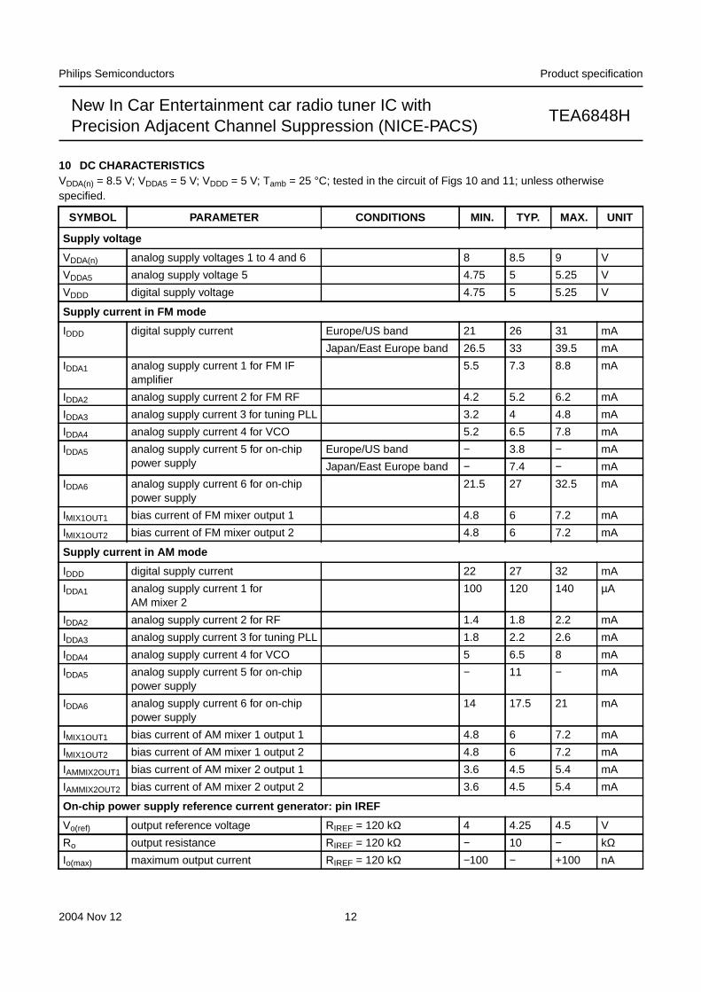
10 DC CHARACTERISTICSVDDA(n) = 8.5 V; VDDA5 = 5 V; VDDD = 5 V; Tamb = 25 °C; tested in the circuit of Figs 10 and 11; unless otherwisespecified.
SYMBOL PARAMETER CONDITIONS MIN. TYP. MAX. UNIT
Supply voltage
VDDA(n) analog supply voltages 1 to 4 and 6 8 8.5 9 V
VDDA5 analog supply voltage 5 4.75 5 5.25 V
VDDD digital supply voltage 4.75 5 5.25 V
Supply current in FM mode
IDDD digital supply current Europe/US band 21 26 31 mA
Japan/East Europe band 26.5 33 39.5 mA
IDDA1 analog supply current 1 for FM IFamplifier
5.5 7.3 8.8 mA
IDDA2 analog supply current 2 for FM RF 4.2 5.2 6.2 mA
IDDA3 analog supply current 3 for tuning PLL 3.2 4 4.8 mA
IDDA4 analog supply current 4 for VCO 5.2 6.5 7.8 mA
IDDA5 analog supply current 5 for on-chippower supply
Europe/US band − 3.8 − mA
Japan/East Europe band − 7.4 − mA
IDDA6 analog supply current 6 for on-chippower supply
21.5 27 32.5 mA
IMIX1OUT1 bias current of FM mixer output 1 4.8 6 7.2 mA
IMIX1OUT2 bias current of FM mixer output 2 4.8 6 7.2 mA
Supply current in AM mode
IDDD digital supply current 22 27 32 mA
IDDA1 analog supply current 1 forAM mixer 2
100 120 140 µA
IDDA2 analog supply current 2 for RF 1.4 1.8 2.2 mA
IDDA3 analog supply current 3 for tuning PLL 1.8 2.2 2.6 mA
IDDA4 analog supply current 4 for VCO 5 6.5 8 mA
IDDA5 analog supply current 5 for on-chippower supply
− 11 − mA
IDDA6 analog supply current 6 for on-chippower supply
14 17.5 21 mA
IMIX1OUT1 bias current of AM mixer 1 output 1 4.8 6 7.2 mA
IMIX1OUT2 bias current of AM mixer 1 output 2 4.8 6 7.2 mA
IAMMIX2OUT1 bias current of AM mixer 2 output 1 3.6 4.5 5.4 mA
IAMMIX2OUT2 bias current of AM mixer 2 output 2 3.6 4.5 5.4 mA
On-chip power supply reference current generator: pin IREF
Vo(ref) output reference voltage RIREF = 120 kΩ 4 4.25 4.5 V
Ro output resistance RIREF = 120 kΩ − 10 − kΩIo(max) maximum output current RIREF = 120 kΩ −100 − +100 nA

2004 Nov 12 13
Philips Semiconductors Product specification
New In Car Entertainment car radio tuner IC withPrecision Adjacent Channel Suppression (NICE-PACS)
TEA6848H
11 AC CHARACTERISTICSVDDA(n) = VMIX1OUT1 = VMIX1OUT2 = VAMMIX2OUT1 = VAMMIX2OUT2 = 8.5 V; VDDD = VDDA5 = 5 V; Tamb = 25 °C; tested in thecircuit of Figs 10 and 11; all AC values are given in RMS; unless otherwise specified.
SYMBOL PARAMETER CONDITIONS MIN. TYP. MAX. UNIT
Voltage controlled oscillator
fosc oscillator frequency 162.9 − 248.2 MHz
C/N carrier-to-noise ratio fosc = 200 MHz; ∆f = 10 kHz − 97 −
RRripple rejection
fripple = 100 Hz;VDDA4(ripple) = 100 mV (RMS);fosc = 200 MHz
92 99 − dB
Crystal oscillator
fxtal crystal frequency − 20.5 − MHz
C/N carrier-to-noise ratio fxtal = 20.5 MHz; ∆f = 10 kHz − 112 −
CIRCUIT INPUTS: PINS XTAL1, XTALGND AND XTAL2
Vo(osc)(rms) oscillator output voltage(RMS value)
note 1 80 100 160 mV
VXTAL1, VXTAL2 DC bias voltage 1.7 2.1 2.5 V
Ri real part of inputimpedance
VXTAL1 − VXTAL2 = 1 mV; note 1 −250 − − Ω
Ci input capacitance note 1 8 10 12 pF
Synthesizer
PROGRAMMABLE DIVIDER
Nprog programmable divider ratio 512 − 32767
∆Nstep programmable divider stepsize
− 1 −
CHARGE PUMP: PIN CPOUT
Isink(cp1)l low charge pump 1 sinkcurrent
0.4 V < VCPOUT < 7.6 V;data byte 3: bit 0 = 0, bit 1 = 1,bit 2 = 1 for FM weather band;fVCO > fref × divider ratio
− 300 − µA
Isource(cp1)l low charge pump 1 sourcecurrent
0.4 V < VCPOUT < 7.6 V;data byte 3: bit 0 = 0, bit 1 = 1,bit 2 = 1 for FM weather band;fVCO < fref × divider ratio
− −300 − µA
Isink(cp1)h high charge pump 1 sinkcurrent
0.4 V < VCPOUT < 7.6 V;data byte 3: bit 0 = 1, bit 1 = 1,bit 2 = 1; AM stereo mode;VCO divider = 10 (LW and MW);fVCO > fref × divider ratio
− 1 − mA
dBc
Hz------------
fosc∆fosc
------------
dBc
Hz------------
2004 Nov 12 14
Philips Semiconductors Product specification
New In Car Entertainment car radio tuner IC withPrecision Adjacent Channel Suppression (NICE-PACS)
TEA6848H
Isource(cp1)h high charge pump 1 sourcecurrent
0.4 V < VCPOUT < 7.6 V;data byte 3: bit 0 = 1, bit 1 = 1,bit 2 = 1; AM stereo mode;VCO divider = 10 (LW and MW);fVCO < fref × divider ratio
− −1 − mA
Isink(cp2) charge pump 2 sink current 0.3 V < VCPOUT < 7.1 V;data byte 3: bit 0 = 0, bit 1 = 0,bit 2 = 0; FM standard mode;fVCO > fref × divider ratio
− 130 − µA
Isource(cp2) charge pump 2 sourcecurrent
0.3 V < VCPOUT < 7.1 V;data byte 3: bit 0 = 0, bit 1 = 0,bit 2 = 0; FM standard mode;fVCO < fref × divider ratio
− −130 − µA
CHARGE PUMP: PIN Vtune
Isink(cp3) charge pump 3 sink current 0.4 V < Vtune < 7.6 V;data byte 3: bit 0 = 0, bit 1 = 0,bit 2 = 0; FM standard mode;fVCO > fref × divider ratio
− 3 − mA
Isource(cp3) charge pump 3 sourcecurrent
0.4 V < Vtune < 7.6 V;data byte 3: bit 0 = 0, bit 1 = 0,bit 2 = 0; FM standard mode;fVCO < fref × divider ratio
− −3 − mA
Antenna Digital Auto Alignment (DAA)
DAA INPUT: PIN DAAIN
Ibias(cp) charge pump buffer inputbias current
VDAAIN = 0.4 to 8 V −10 − +10 nA
Vi(cp) charge pump buffer inputvoltage
0 − 8.5 V
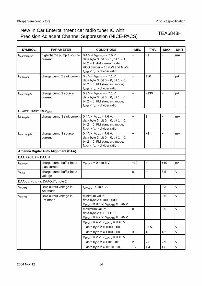
DAA OUTPUT: PIN DAAOUT; note 2
Vo(AM) DAA output voltage inAM mode
IDAAOUT < 100 µA − − 0.3 V
Vo(FM) DAA output voltage inFM mode
minimum value;data byte 2 = 10000000;VDAAIN = 0.5 V; VDAATD = 0.45 V
− − 0.5 V
maximum value;data byte 2 = 11111111;VDAAIN = 4.7 V; VDAATD = 0.45 V
8 − 8.5 V
VDAAIN = 4 V; VDAATD = 0.45 V
data byte 2 = 10000000 − 0.65 − V
data byte 2 = 11000000 3.8 4 4.2 V
VDAAIN = 2 V; VDAATD = 0.45 V
data byte 2 = 11010101 2.3 2.6 2.9 V
data byte 2 = 10101010 1.2 1.4 1.6 V
SYMBOL PARAMETER CONDITIONS MIN. TYP. MAX. UNIT
2004 Nov 12 15
Philips Semiconductors Product specification
New In Car Entertainment car radio tuner IC withPrecision Adjacent Channel Suppression (NICE-PACS)
TEA6848H
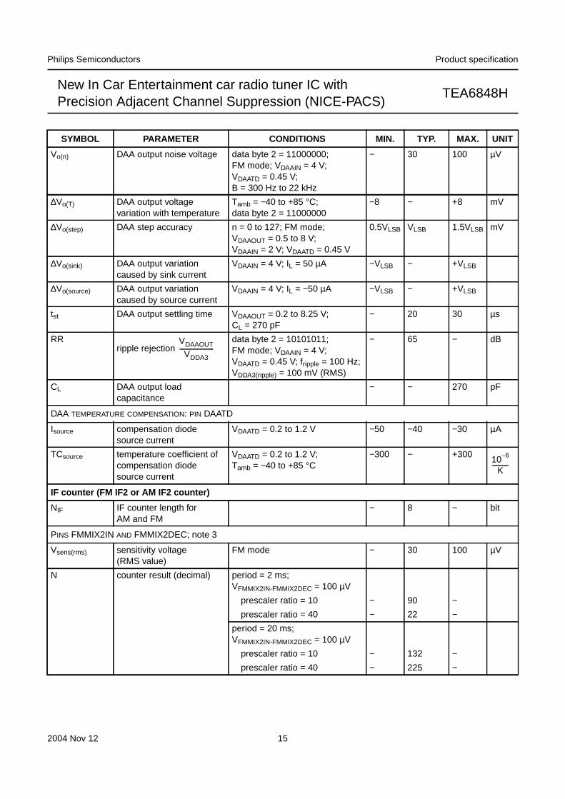
Vo(n) DAA output noise voltage data byte 2 = 11000000;FM mode; VDAAIN = 4 V;VDAATD = 0.45 V;B = 300 Hz to 22 kHz
− 30 100 µV
∆Vo(T) DAA output voltagevariation with temperature
Tamb = −40 to +85 °C;data byte 2 = 11000000
−8 − +8 mV
∆Vo(step) DAA step accuracy n = 0 to 127; FM mode;VDAAOUT = 0.5 to 8 V;VDAAIN = 2 V; VDAATD = 0.45 V
0.5VLSB VLSB 1.5VLSB mV
∆Vo(sink) DAA output variationcaused by sink current
VDAAIN = 4 V; IL = 50 µA −VLSB − +VLSB
∆Vo(source) DAA output variationcaused by source current
VDAAIN = 4 V; IL = −50 µA −VLSB − +VLSB
tst DAA output settling time VDAAOUT = 0.2 to 8.25 V;CL = 270 pF
− 20 30 µs
RRripple rejection
data byte 2 = 10101011;FM mode; VDAAIN = 4 V;VDAATD = 0.45 V; fripple = 100 Hz;VDDA3(ripple) = 100 mV (RMS)
− 65 − dB
CL DAA output loadcapacitance
− − 270 pF
DAA TEMPERATURE COMPENSATION: PIN DAATD
Isource compensation diodesource current
VDAATD = 0.2 to 1.2 V −50 −40 −30 µA
TCsource temperature coefficient ofcompensation diodesource current
VDAATD = 0.2 to 1.2 V;Tamb = −40 to +85 °C
−300 − +300
IF counter (FM IF2 or AM IF2 counter)
NIF IF counter length forAM and FM
− 8 − bit
PINS FMMIX2IN AND FMMIX2DEC; note 3
Vsens(rms) sensitivity voltage(RMS value)
FM mode − 30 100 µV
N counter result (decimal) period = 2 ms;VFMMIX2IN-FMMIX2DEC = 100 µV
prescaler ratio = 10 − 90 −prescaler ratio = 40 − 22 −
period = 20 ms;VFMMIX2IN-FMMIX2DEC = 100 µV
prescaler ratio = 10 − 132 −prescaler ratio = 40 − 225 −
SYMBOL PARAMETER CONDITIONS MIN. TYP. MAX. UNIT
VDAAOUT
VDDA3-----------------------
10 6–
K-----------
2004 Nov 12 16
Philips Semiconductors Product specification
New In Car Entertainment car radio tuner IC withPrecision Adjacent Channel Suppression (NICE-PACS)
TEA6848H
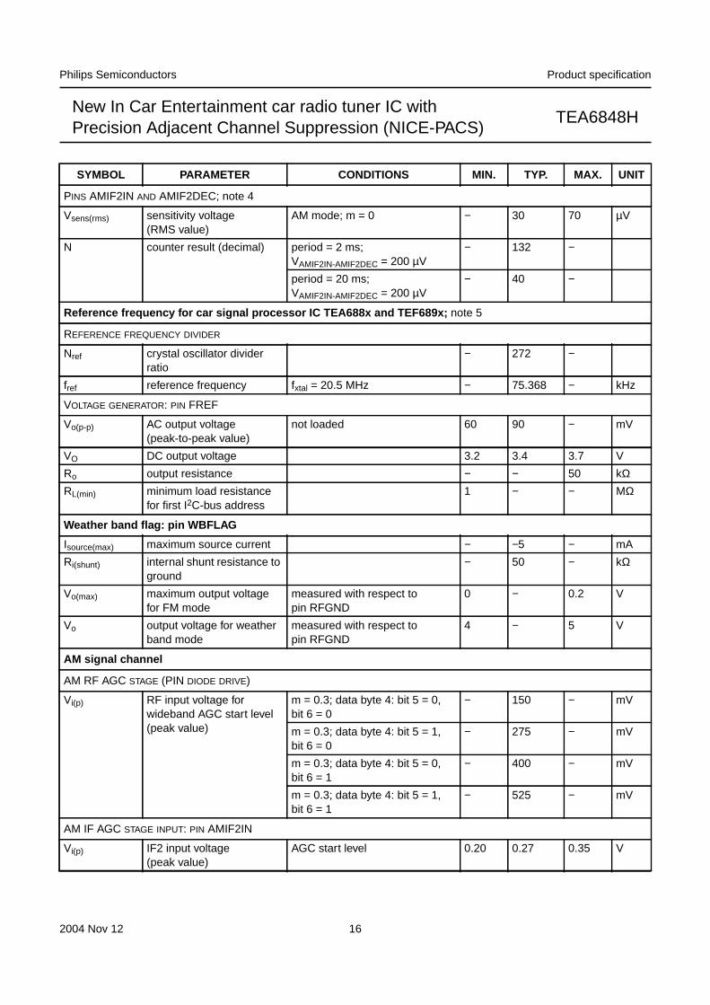
PINS AMIF2IN AND AMIF2DEC; note 4
Vsens(rms) sensitivity voltage(RMS value)
AM mode; m = 0 − 30 70 µV
N counter result (decimal) period = 2 ms;VAMIF2IN-AMIF2DEC = 200 µV
− 132 −
period = 20 ms;VAMIF2IN-AMIF2DEC = 200 µV
− 40 −
Reference frequency for car signal processor IC TEA688x and TEF689x; note 5
REFERENCE FREQUENCY DIVIDER
Nref crystal oscillator dividerratio
− 272 −
fref reference frequency fxtal = 20.5 MHz − 75.368 − kHz
VOLTAGE GENERATOR: PIN FREF
Vo(p-p) AC output voltage(peak-to-peak value)
not loaded 60 90 − mV
VO DC output voltage 3.2 3.4 3.7 V
Ro output resistance − − 50 kΩRL(min) minimum load resistance
for first I2C-bus address1 − − MΩ
Weather band flag: pin WBFLAG
Isource(max) maximum source current − −5 − mA
Ri(shunt) internal shunt resistance toground
− 50 − kΩ
Vo(max) maximum output voltagefor FM mode
measured with respect topin RFGND
0 − 0.2 V
Vo output voltage for weatherband mode
measured with respect topin RFGND
4 − 5 V
AM signal channel
AM RF AGC STAGE (PIN DIODE DRIVE)
Vi(p) RF input voltage forwideband AGC start level(peak value)
m = 0.3; data byte 4: bit 5 = 0,bit 6 = 0
− 150 − mV
m = 0.3; data byte 4: bit 5 = 1,bit 6 = 0
− 275 − mV
m = 0.3; data byte 4: bit 5 = 0,bit 6 = 1
− 400 − mV
m = 0.3; data byte 4: bit 5 = 1,bit 6 = 1
− 525 − mV
AM IF AGC STAGE INPUT: PIN AMIF2IN
Vi(p) IF2 input voltage(peak value)
AGC start level 0.20 0.27 0.35 V
SYMBOL PARAMETER CONDITIONS MIN. TYP. MAX. UNIT
2004 Nov 12 17
Philips Semiconductors Product specification
New In Car Entertainment car radio tuner IC withPrecision Adjacent Channel Suppression (NICE-PACS)
TEA6848H
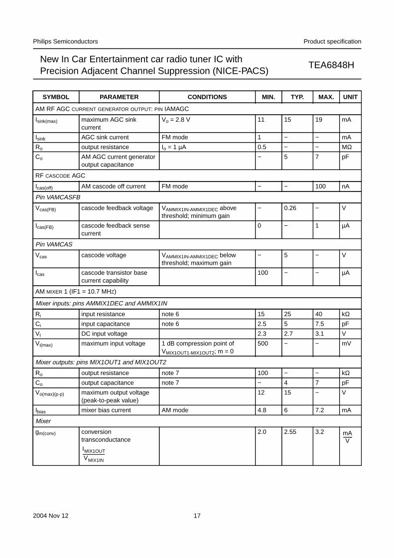
AM RF AGC CURRENT GENERATOR OUTPUT: PIN IAMAGC
Isink(max) maximum AGC sinkcurrent
Vo = 2.8 V 11 15 19 mA
Isink AGC sink current FM mode 1 − − mA
Ro output resistance Io = 1 µA 0.5 − − MΩCo AM AGC current generator
output capacitance− 5 7 pF
RF CASCODE AGC
Icas(off) AM cascode off current FM mode − − 100 nA
Pin VAMCASFB
Vcas(FB) cascode feedback voltage VAMMIX1IN-AMMIX1DEC abovethreshold; minimum gain
− 0.26 − V
Icas(FB) cascode feedback sensecurrent
0 − 1 µA
Pin VAMCAS
Vcas cascode voltage VAMMIX1IN-AMMIX1DEC belowthreshold; maximum gain
− 5 − V
Icas cascode transistor basecurrent capability
100 − − µA
AM MIXER 1 (IF1 = 10.7 MHZ)
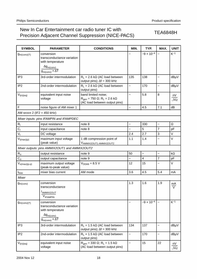
Mixer inputs: pins AMMIX1DEC and AMMIX1IN
Ri input resistance note 6 15 25 40 kΩCi input capacitance note 6 2.5 5 7.5 pF
VI DC input voltage 2.3 2.7 3.1 V
Vi(max) maximum input voltage 1 dB compression point ofVMIX1OUT1-MIX1OUT2; m = 0
500 − − mV
Mixer outputs: pins MIX1OUT1 and MIX1OUT2
Ro output resistance note 7 100 − − kΩCo output capacitance note 7 − 4 7 pF
Vo(max)(p-p) maximum output voltage(peak-to-peak value)
12 15 − V
Ibias mixer bias current AM mode 4.8 6 7.2 mA
Mixer
gm(conv) conversiontransconductance
2.0 2.55 3.2
SYMBOL PARAMETER CONDITIONS MIN. TYP. MAX. UNIT
IMIX1OUT
VMIX1IN---------------------
mAV
---------
2004 Nov 12 18
Philips Semiconductors Product specification
New In Car Entertainment car radio tuner IC withPrecision Adjacent Channel Suppression (NICE-PACS)
TEA6848H
gm(conv)(T) conversiontransconductance variationwith temperature
− −9 × 10⁻⁴ − K−1
IP3 3rd-order intermodulation RL = 2.6 kΩ (AC load betweenoutput pins); ∆f = 300 kHz
135 138 − dBµV
IP2 2nd-order intermodulation RL = 2.6 kΩ (AC load betweenoutput pins)
− 170 − dBµV
Vi(n)(eq) equivalent input noisevoltage
band limited noise;Rgen = 750 Ω; RL = 2.6 kΩ(AC load between output pins)
− 5.8 8
F noise figure of AM mixer 1 − 4.5 7.1 dB
AM MIXER 2 (IF2 = 450 kHz)
Mixer inputs: pins IFAMPIN and IFAMPDEC
Ri input resistance note 8 − 330 − ΩCi input capacitance note 8 − 5 7 pF
VI DC voltage 2.4 2.7 3 V
Vi(max)(p) maximum input voltage(peak value)
1 dB compression point ofVAMMIX2OUT1-AMMIX2OUT2
1.1 1.4 − V
Mixer outputs: pins AMMIX2OUT1 and AMMIX2OUT2
Ro output resistance note 9 50 − − kΩCo output capacitance note 9 − 4 7 pF
Vo(max)(p-p) maximum output voltage(peak-to-peak value)
VDDA6 = 8.5 V 12 15 − V
Ibias mixer bias current AM mode 3.6 4.5 5.4 mA
Mixer
gm(conv) conversiontransconductance
1.3 1.6 1.9
gm(conv)(T) conversiontransconductance variationwith temperature
− −9 × 10⁻⁴ − K−1
IP3 3rd-order intermodulation RL = 1.5 kΩ (AC load betweenoutput pins); ∆f = 300 kHz
134 137 − dBµV
IP2 2nd-order intermodulation RL = 1.5 kΩ (AC load betweenoutput pins)
− 170 − dBµV
Vi(n)(eq) equivalent input noisevoltage
Rgen = 330 Ω; RL = 1.5 kΩ(AC load between output pins)
− 15 22
SYMBOL PARAMETER CONDITIONS MIN. TYP. MAX. UNIT
gm(conv)∆gm(conv) T∆×---------------------------------
nV
Hz------------
IAMMIX2OUT
VIFAMPIN----------------------------
mAV
---------
gm(conv)∆gm(conv) T∆×---------------------------------
nV
Hz------------
2004 Nov 12 19
Philips Semiconductors Product specification
New In Car Entertainment car radio tuner IC withPrecision Adjacent Channel Suppression (NICE-PACS)
TEA6848H
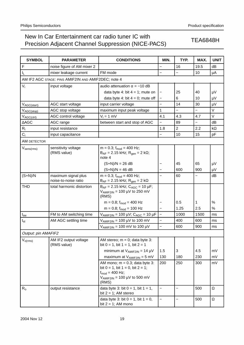
F noise figure of AM mixer 2 − 16 19.5 dB
IL mixer leakage current FM mode − − 10 µA
AM IF2 AGC STAGE: PINS AMIF2IN AND AMIF2DEC; note 4
Vi input voltage audio attenuation α = −10 dB
data byte 4: bit 4 = 1; mute on − 25 40 µV
data byte 4: bit 4 = 0; mute off − 6 10 µV
VAGC(start) AGC start voltage input carrier voltage − 14 30 µV
VAGC(stop) AGC stop voltage maximum input peak voltage 1 − − V
VAGC(ctrl) AGC control voltage Vi = 1 mV 4.1 4.3 4.7 V
∆AGC AGC range between start and stop of AGC − 89 − dB
Ri input resistance 1.8 2 2.2 kΩCi input capacitance − 10 15 pF
AM DETECTOR
Vsens(rms) sensitivity voltage(RMS value)
m = 0.3; fmod = 400 Hz;BAF = 2.15 kHz; Rgen = 2 kΩ;note 4
(S+N)/N = 26 dB − 45 65 µV
(S+N)/N = 46 dB − 600 900 µV
(S+N)/N maximum signal plusnoise-to-noise ratio
m = 0.3; fmod = 400 Hz;BAF = 2.15 kHz; Rgen = 2 kΩ
− 60 − dB
THD total harmonic distortion BAF = 2.15 kHz; CAGC = 10 µF;VAMIF2IN = 100 µV to 250 mV(RMS)
m = 0.8; fmod = 400 Hz − 0.5 1 %
m = 0.8; fmod = 100 Hz − 1.25 2.5 %
tsw FM to AM switching time VAMIF2IN = 100 µV; CAGC = 10 µF − 1000 1500 ms
tst AM AGC settling time VAMIF2IN = 100 µV to 100 mV − 400 600 ms
VAMIF2IN = 100 mV to 100 µV − 600 900 ms
Output: pin AMAFIF2
Vo(rms) AM IF2 output voltage(RMS value)
AM stereo; m = 0; data byte 3:bit 0 = 1, bit 1 = 1, bit 2 = 1
minimum at VAMIF2IN = 14 µV 1.5 3 4.5 mV
maximum at VAMIF2IN = 5 mV 130 180 230 mV
AM mono; m = 0.3; data byte 3:bit 0 = 1, bit 1 = 0, bit 2 = 1;fmod = 400 Hz;VAMIF2IN = 100 µV to 500 mV(RMS)
200 250 300 mV
Ro output resistance data byte 3: bit 0 = 1, bit 1 = 1,bit 2 = 1; AM stereo
− − 500 Ω
data byte 3: bit 0 = 1, bit 1 = 0,bit 2 = 1; AM mono
− − 500 Ω
SYMBOL PARAMETER CONDITIONS MIN. TYP. MAX. UNIT
2004 Nov 12 20
Philips Semiconductors Product specification
New In Car Entertainment car radio tuner IC withPrecision Adjacent Channel Suppression (NICE-PACS)
TEA6848H
Co output capacitance data byte 3: bit 0 = 1, bit 1 = 0,bit 2 = 1
− 5 7 pF
ZL load impedance data byte 3: bit 0 = 1, bit 1 = 0,bit 2 = 1; AM mono
100 − − kΩ
data byte 3: bit 0 = 1, bit 1 = 1,bit 2 = 1; AM stereo
10 − − kΩ
RR ripple rejection VDDA5(ripple) = 100 mV (RMS);fripple = 100 Hz
− 24 − dB
VDDA6(ripple) = 100 mV (RMS);fripple = 100 Hz
− 26 − dB
AM IF2 LEVEL DETECTOR OUTPUT: PIN Vlevel(AMFM); see Fig.4
Vlevel(AMFM) DC output voltage VAMIF2IN = 10 µV to 1 V 0 − 7 V
VAMIF2IN < 1 µV; standard settingof level DAA
0.1 0.5 0.9 V
VAMIF2IN = 1.4 mV; standardsetting of level DAA
1.6 2.2 2.8 V
∆Vlevel(AMFM) step size for adjustment oflevel starting point
VAMIF2IN = 0 V; standard settingof level slope
30 40 50 mV
Vlevel(slope) slope of level voltage VAMIF2IN = 140 µV to 140 mV;standard setting of level slope
650 800 950
∆Vstep step size for adjustment oflevel slope
VAMIF2IN = 1.4 mV 45 60 75
Blevel(AMFM) bandwidth of level outputvoltage
VAMIF2IN = 15 mV; standardsetting of level DAA
200 300 − kHz
Ro output resistance − − 500 ΩRR
ripple rejectionVDDA6(ripple) = 100 mV (RMS);fripple = 100 Hz
− 36 − dB
AM NOISE BLANKER; TEST SIGNAL AND TEST CIRCUIT; see Fig.5
Threshold: pin AMNBHOLD
VO DC output voltage 4.3 4.6 5.1 V
tsup suppression time Vpulse = 200 mV (peak);Vlevel(AMFM) < 1.8 V
6 7.5 10 µs
ftrigger trigger sensitivity frequency Vpulse = 200 mV (peak);Vleve(AMFM)l < 1.8 V
− 1000 − Hz
Vpulse = 200 mV (peak);Vlevel(AMFM) > 2.2 V
− − 100 Hz
Vpulse = 20 mV (peak);Vlevel(AMFM) < 1.8 V
− − 100 Hz
Noise detector output: pin TRDSMUTE
Isink(AGC) AM noise blanker AGC sinkcurrent
VTRDSMUTE = 3 V 35 50 65 µA
SYMBOL PARAMETER CONDITIONS MIN. TYP. MAX. UNIT
mV20 dB---------------
mV20 dB---------------
Vlevel
VDDA6----------------
2004 Nov 12 21
Philips Semiconductors Product specification
New In Car Entertainment car radio tuner IC withPrecision Adjacent Channel Suppression (NICE-PACS)
TEA6848H
VAGC AM noise blanker AGCvoltage
AM mixer 1 input Vi = 0 V 1.9 2.2 2.5 V
FM signal channel
FM RF AGC (FM DISTANCE MODE; DATA BYTE 4: BIT 3 = 0)
Inputs: pins FMMIXIN1 and FMMIXIN2; note 10
Vi(RF)(rms) RF input voltage for start ofwideband AGC(RMS value)
data byte 4: bit 5 = 1, bit 6 = 1 − 3 − mV
data byte 4: bit 5 = 0, bit 6 = 1 − 6 − mV
data byte 4: bit 5 = 1, bit 6 = 0 − 9 − mV
data byte 4: bit 5 = 0, bit 6 = 0 − 12 − mV
Pin TFMAGC
Rsource source resistance 4 5 6 kΩVO(ref) DC output reference
voltagedata byte 4: bit 5 = 0, bit 6 = 0;VFMMIXIN1-FMMIXIN2 = 0 V
4.1 4.6 5.1 V
PIN diode drive output: pin IFMAGC
Isink(AGC)(max) maximum AGC sinkcurrent
VIFMAGC = 2.5 V;VTFMAGC = VO(ref) − 0.5 V;data byte 4: bit 5 = 0, bit 6 = 0,bit 7 = 0
8 11.5 15 mA
Isource(AGC)(max) maximum AGC sourcecurrent
VIFMAGC = 2.5 V;VTFMAGC = VO(ref) + 0.5 V;data byte 4: bit 5 = 0, bit 6 = 0,bit 7 = 0
−15 −11.5 −8 mA
Isource(AGC) AGC source current AM mode −15 −11.5 −8 mA
VIFMAGC = 2.5 V; data byte 4:bit 3 = 1 (FM local)
−0.65 −0.5 −0.35 mA
Level voltage output: pin Vlevel(AMFM)
Vth threshold voltage fornarrow-band AGC
data byte 4: bit 5 = 0, bit 6 = 0,bit 7 = 1; keyed AGC
500 950 1400 mV
FM RF MIXER
Reference voltage: pin Vref(MIX)
Vref reference voltage FM mode 6.5 7.1 7.9 V
AM mode 2.7 3.1 3.4 V
Inputs: pins FMMIXIN1 and FMMIXIN2; note 10
Vi(RF)(max) maximum RF input voltage 1 dB compression point ofFM mixer output voltage(peak-to-peak value)
70 100 − mV
Vi(n)(eq) equivalent input noisevoltage
Rgen = 200 Ω; RL = 2.6 kΩ − 2.6 3.1
Ri input resistance 1.4 2.8 4.2 kΩCi input capacitance − 5 7 pF
SYMBOL PARAMETER CONDITIONS MIN. TYP. MAX. UNIT
nV
Hz------------
2004 Nov 12 22
Philips Semiconductors Product specification
New In Car Entertainment car radio tuner IC withPrecision Adjacent Channel Suppression (NICE-PACS)
TEA6848H
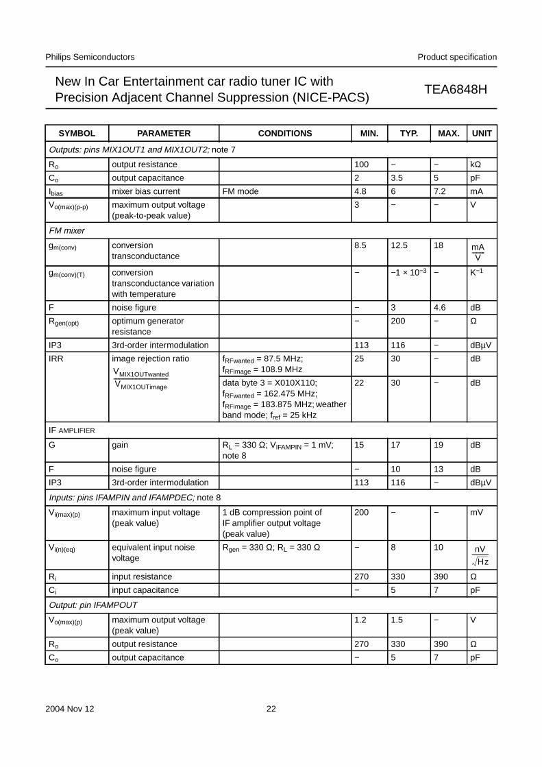
Outputs: pins MIX1OUT1 and MIX1OUT2; note 7
Ro output resistance 100 − − kΩCo output capacitance 2 3.5 5 pF
Ibias mixer bias current FM mode 4.8 6 7.2 mA
Vo(max)(p-p) maximum output voltage(peak-to-peak value)
3 − − V
FM mixer
gm(conv) conversiontransconductance
8.5 12.5 18
gm(conv)(T) conversiontransconductance variationwith temperature
− −1 × 10⁻³ − K−1
F noise figure − 3 4.6 dB
Rgen(opt) optimum generatorresistance
− 200 − Ω
IP3 3rd-order intermodulation 113 116 − dBµV
IRR image rejection ratio fRFwanted = 87.5 MHz;fRFimage = 108.9 MHz
25 30 − dB
data byte 3 = X010X110;fRFwanted = 162.475 MHz;fRFimage = 183.875 MHz; weatherband mode; fref = 25 kHz
22 30 − dB
IF AMPLIFIER
G gain RL = 330 Ω; VIFAMPIN = 1 mV;note 8
15 17 19 dB
F noise figure − 10 13 dB
IP3 3rd-order intermodulation 113 116 − dBµV
Inputs: pins IFAMPIN and IFAMPDEC; note 8
Vi(max)(p) maximum input voltage(peak value)
1 dB compression point ofIF amplifier output voltage(peak value)
200 − − mV
Vi(n)(eq) equivalent input noisevoltage
Rgen = 330 Ω; RL = 330 Ω − 8 10
Ri input resistance 270 330 390 ΩCi input capacitance − 5 7 pF
Output: pin IFAMPOUT
Vo(max)(p) maximum output voltage(peak value)
1.2 1.5 − V
Ro output resistance 270 330 390 ΩCo output capacitance − 5 7 pF
SYMBOL PARAMETER CONDITIONS MIN. TYP. MAX. UNIT
mAV
---------
VMIX1OUTwanted
VMIX1OUTimage--------------------------------------
nV
Hz------------
2004 Nov 12 23
Philips Semiconductors Product specification
New In Car Entertainment car radio tuner IC withPrecision Adjacent Channel Suppression (NICE-PACS)
TEA6848H
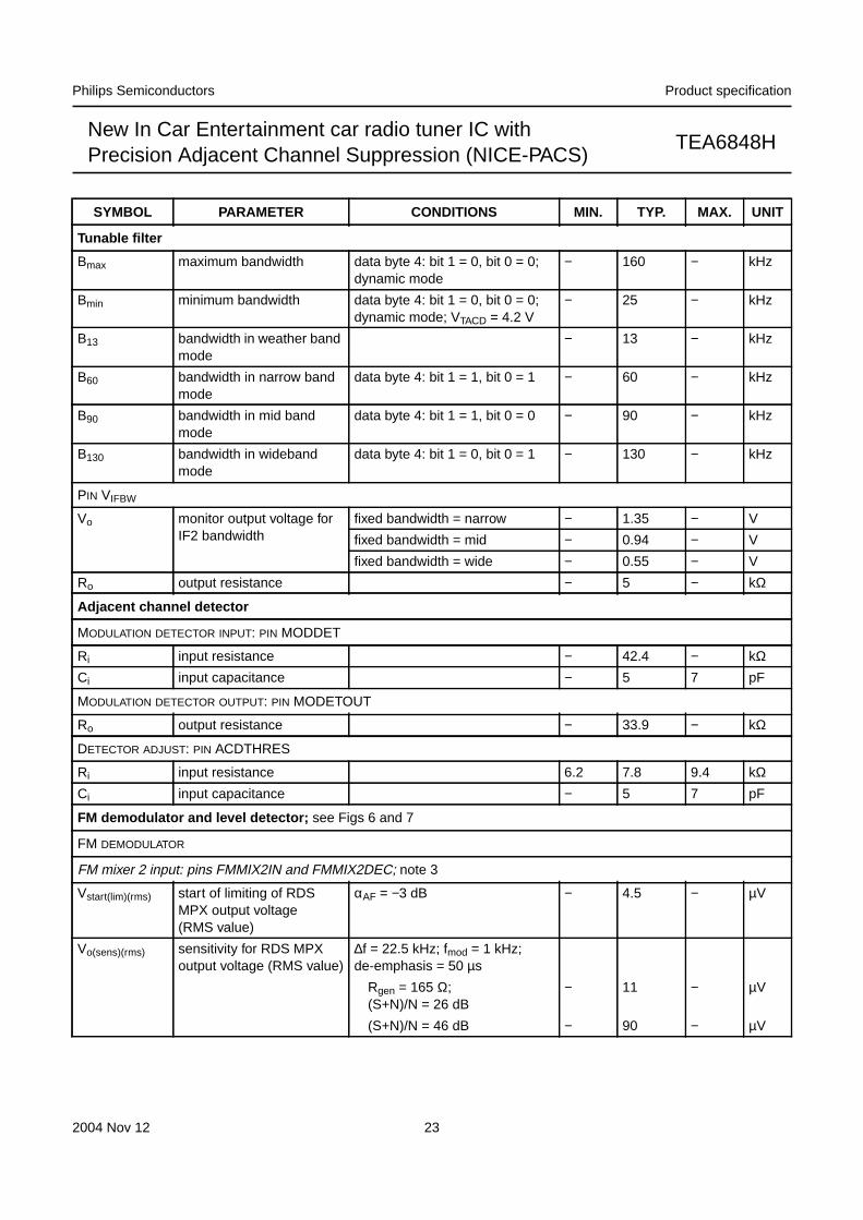
Tunable filter
Bmax maximum bandwidth data byte 4: bit 1 = 0, bit 0 = 0;dynamic mode
− 160 − kHz
Bmin minimum bandwidth data byte 4: bit 1 = 0, bit 0 = 0;dynamic mode; VTACD = 4.2 V
− 25 − kHz
B13 bandwidth in weather bandmode
− 13 − kHz
B60 bandwidth in narrow bandmode
data byte 4: bit 1 = 1, bit 0 = 1 − 60 − kHz
B90 bandwidth in mid bandmode
data byte 4: bit 1 = 1, bit 0 = 0 − 90 − kHz
B130 bandwidth in widebandmode
data byte 4: bit 1 = 0, bit 0 = 1 − 130 − kHz
PIN VIFBW
Vo monitor output voltage forIF2 bandwidth
fixed bandwidth = narrow − 1.35 − V
fixed bandwidth = mid − 0.94 − V
fixed bandwidth = wide − 0.55 − V
Ro output resistance − 5 − kΩ
Adjacent channel detector
MODULATION DETECTOR INPUT: PIN MODDET
Ri input resistance − 42.4 − kΩCi input capacitance − 5 7 pF
MODULATION DETECTOR OUTPUT: PIN MODETOUT
Ro output resistance − 33.9 − kΩ
DETECTOR ADJUST: PIN ACDTHRES
Ri input resistance 6.2 7.8 9.4 kΩCi input capacitance − 5 7 pF
FM demodulator and level detector; see Figs 6 and 7
FM DEMODULATOR
FM mixer 2 input: pins FMMIX2IN and FMMIX2DEC; note 3
Vstart(lim)(rms) start of limiting of RDSMPX output voltage(RMS value)
αAF = −3 dB − 4.5 − µV
Vo(sens)(rms) sensitivity for RDS MPXoutput voltage (RMS value)
∆f = 22.5 kHz; fmod = 1 kHz;de-emphasis = 50 µs
Rgen = 165 Ω;(S+N)/N = 26 dB
− 11 − µV
(S+N)/N = 46 dB − 90 − µV
SYMBOL PARAMETER CONDITIONS MIN. TYP. MAX. UNIT
2004 Nov 12 24
Philips Semiconductors Product specification
New In Car Entertainment car radio tuner IC withPrecision Adjacent Channel Suppression (NICE-PACS)
TEA6848H
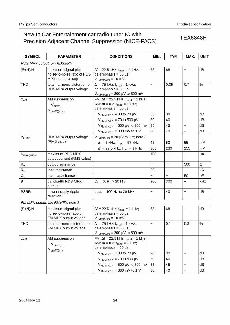
RDS MPX output: pin RDSMPX
(S+N)/N maximum signal plusnoise-to-noise ratio of RDSMPX output voltage
∆f = 22.5 kHz; fmod = 1 kHz;de-emphasis = 50 µs;VFMMIX2IN = 10 mV
65 68 − dB
THD total harmonic distortion ofRDS MPX output voltage
∆f = 75 kHz; fmod = 1 kHz;de-emphasis = 50 µs;VFMMIX2IN = 200 µV to 800 mV
− 0.35 0.7 %
αAM AM suppression FM: ∆f = 22.5 kHz; fmod = 1 kHz;AM: m = 0.3; fmod = 1 kHz;de-emphasis = 50 µs
VFMMIX2IN = 30 to 70 µV 20 30 − dB
VFMMIX2IN = 70 to 500 µV 30 40 − dB
VFMMIX2IN = 500 µV to 300 mV 35 45 − dB
VFMMIX2IN = 300 mV to 1 V 30 40 − dB
Vo(rms) RDS MPX output voltage(RMS value)
VFMMIX2IN = 20 µV to 1 V; note 3
∆f = 5 kHz; fmod = 57 kHz 45 50 55 mV
∆f = 22.5 kHz; fmod = 1 kHz 205 230 255 mV
Io(max)(rms) maximum RDS MPXoutput current (RMS value)
100 − − µA
Ro output resistance − − 500 ΩRL load resistance 20 − − kΩCL load capacitance − − 50 pF
B bandwidth RDS MPXoutput
CL = 0; RL > 20 kΩ 200 300 − kHz
PSRR power supply ripplerejection
fripple = 100 Hz to 20 kHz − 40 − dB
FM MPX output: pin FMMPX; note 3
(S+N)/N maximum signal plusnoise-to-noise ratio ofFM MPX output voltage
∆f = 22.5 kHz; fmod = 1 kHz;de-emphasis = 50 µs;VFMMIX2IN = 10 mV
65 68 − dB
THD total harmonic distortion ofFM MPX output voltage
∆f = 75 kHz; fmod = 1 kHz;de-emphasis = 50 µs;VFMMIX2IN = 200 µV to 800 mV
− 0.1 0.3 %
αAM AM suppression FM: ∆f = 22.5 kHz; fmod = 1 kHz;AM: m = 0.3; fmod = 1 kHz;de-emphasis = 50 µs
VFMMIX2IN = 30 to 70 µV 20 30 − dB
VFMMIX2IN = 70 to 500 µV 30 40 − dB
VFMMIX2IN = 500 µV to 300 mV 35 45 − dB
VFMMIX2IN = 300 mV to 1 V 30 40 − dB
SYMBOL PARAMETER CONDITIONS MIN. TYP. MAX. UNIT
Vo(rms)
Vo(AM)(rms)---------------------------
Vo(rms)
Vo(AM)(rms)---------------------------
2004 Nov 12 25
Philips Semiconductors Product specification
New In Car Entertainment car radio tuner IC withPrecision Adjacent Channel Suppression (NICE-PACS)
TEA6848H
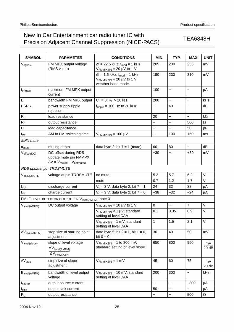
Vo(rms) FM MPX output voltage(RMS value)
∆f = 22.5 kHz; fmod = 1 kHz;VFMMIX2IN = 20 µV to 1 V
205 230 255 mV
∆f = 1.5 kHz; fmod = 1 kHz;VFMMIX2IN = 20 µV to 1 V;weather band mode
150 230 310 mV
Io(max) maximum FM MPX outputcurrent
100 − − µA
B bandwidth FM MPX output CL = 0; RL > 20 kΩ 200 − − kHz
PSRR power supply ripplerejection
fripple = 100 Hz to 20 kHz − 40 − dB
RL load resistance 20 − − kΩRo output resistance − − 500 ΩCL load capacitance − − 50 pF
tsw AM to FM switching time VFMMIX2IN = 100 µV − 100 150 ms
MPX mute
αmute muting depth data byte 2: bit 7 = 1 (mute) 60 80 − dB
Voffset(DC) DC offset during RDSupdate mute pin FMMPX∆V = Vmuted − Vnotmuted
−30 − +30 mV
RDS update: pin TRDSMUTE
VTRDSMUTE voltage at pin TRDSMUTE no mute 5.2 5.7 6.2 V
mute 0.7 1.2 1.7 V
Idch discharge current Vo = 3 V; data byte 2: bit 7 = 1 24 32 38 µA
Ich charge current Vo = 3 V; data byte 2: bit 7 = 0 −38 −32 −24 µA
FM IF LEVEL DETECTOR OUTPUT: PIN Vlevel(AMFM); note 3
Vlevel(AMFM) DC output voltage VFMMIX2IN = 10 µV to 1 V 0 − 7 V
VFMMIX2IN < 1 µV; standardsetting of level DAA
0.1 0.35 0.9 V
VFMMIX2IN = 1 mV; standardsetting of level DAA
1 1.5 2.1 V
∆Vlevel(AMFM) step size of starting pointadjustment
data byte 5: bit 2 = 1, bit 1 = 0,bit 0 = 0
30 40 50 mV
Vlevel(slope) slope of level voltage VFMMIX2IN = 1 to 300 mV;standard setting of level slope
650 800 950
∆Vstep step size of slopeadjustment
VFMMIX2IN = 1 mV 45 60 75
Blevel(AMFM) bandwidth of level outputvoltage
VFMMIX2IN = 10 mV; standardsetting of level DAA
200 300 − kHz
Isource output source current − − −300 µA
Isink output sink current 50 − − µA
Ro output resistance − − 500 Ω
SYMBOL PARAMETER CONDITIONS MIN. TYP. MAX. UNIT
∆Vlevel(AMFM)
∆VFMMIX2IN---------------------------------
mV20 dB---------------
mV20 dB---------------
2004 Nov 12 26
Philips Semiconductors Product specification
New In Car Entertainment car radio tuner IC withPrecision Adjacent Channel Suppression (NICE-PACS)
TEA6848H
Notes
1. Measured between pins XTAL1 and XTAL2.
2. DAA conversion gain formula: ; where
n = 0 to 127.
3. Input parameters of FM mixer 2 measured between pins FMMIX2IN and FMMIX2DEC.
4. Input parameters of AM IF2 measured between pins AMIF2IN and AMIF2DEC.
5. Reference frequency pin FREF: Rext = 68 kΩ connected to ground activates the 2nd I2C-bus address.
6. Input parameters of AM mixer 1 measured between pins AMMIX1DEC and AMMIX1IN.
7. Output parameters of FM mixer and AM mixer 1 measured between pins MIX1OUT1 and MIX1OUT2.
8. Input parameters of AM mixer 2 measured between pins IFAMPIN and IFAMPDEC.
9. Output parameters of AM mixer 2 measured between pins AMMIX2OUT1 and AMMIX2OUT2.
10. Input parameters of FM mixer measured between pins FMMIXIN1 and FMMIXIN2.
RR ripple rejection fripple = 100 Hz;VDDA6(ripple) = 100 mV (RMS)
− 40 − dB
PIN Vlevel(ACD)
Ro output resistance 6.4 8 9.6 kΩ
RDS update
Output: pin AFHOLD
Isink(max) maximum sink current after first bus transmission withdata byte 0: bit 7 = 1 (start ofRDS update); Vo = 0.5 V
1.0 1.2 1.4 mA
Output: pin AFSAMPLE
Isink(max) maximum sink current no RDS update in progress;Vo = 0.5 V
1.0 1.2 1.4 mA
SYMBOL PARAMETER CONDITIONS MIN. TYP. MAX. UNIT
VDAAOUT 2 0.75 n128---------- 0.125+×
× VDAAIN VDAATD+( )× VDAATD–=
2004 Nov 12 27
Philips Semiconductors Product specification
New In Car Entertainment car radio tuner IC withPrecision Adjacent Channel Suppression (NICE-PACS)
TEA6848H
handbook, full pagewidth10
0
8
THD(%)
7
6
5
4
3
2
1
0−70
−60
−50
−40
−30
−20
−10
MHC438
10−3 10−2 10−1
VAMIF2IN (mV)1
(1)
(6)
10 102 103
VAMAFIF2(dB)
(3)
(5)
(4)
(2)
Vlevel(AMFM) (V)
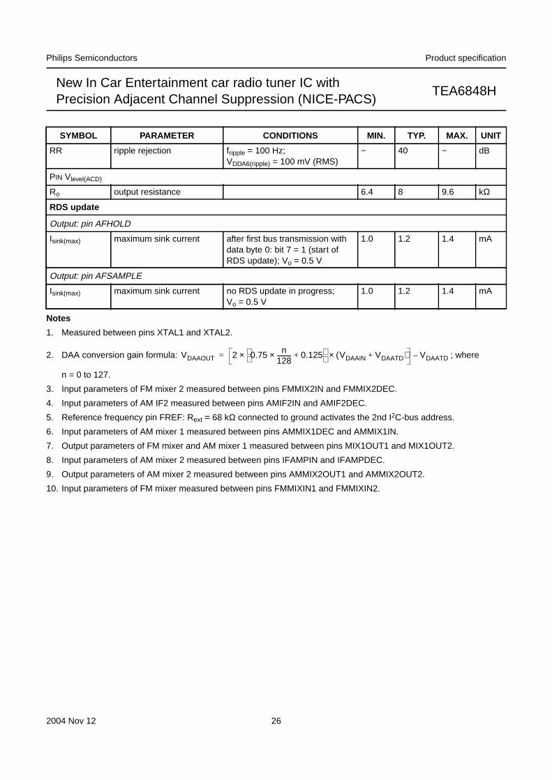
Fig.3 AM detector and level output.
(1) AF: fIF = 450 kHz; m = 0.3; fmod = 1 kHz; soft mute off.
(2) AF: fIF = 450 kHz; m = 0.3; fmod = 1 kHz; soft mute on.
(3) Noise: unweighted B = 2.15 kHz; soft mute off.
(4) Noise: unweighted B = 2.15 kHz; soft mute on.
(5) Level detector output voltage, default setting.
(6) THD: m = 0.8.
2004 Nov 12 28
Philips Semiconductors Product specification
New In Car Entertainment car radio tuner IC withPrecision Adjacent Channel Suppression (NICE-PACS)
TEA6848H
handbook, full pagewidth6
2
010−3 10−2 10−1 1 10 102 103
MHC439
4
3
1
5
VAMIF2IN (mV)
(2)
(3)
(1)
Vlevel(AMFM)(V)
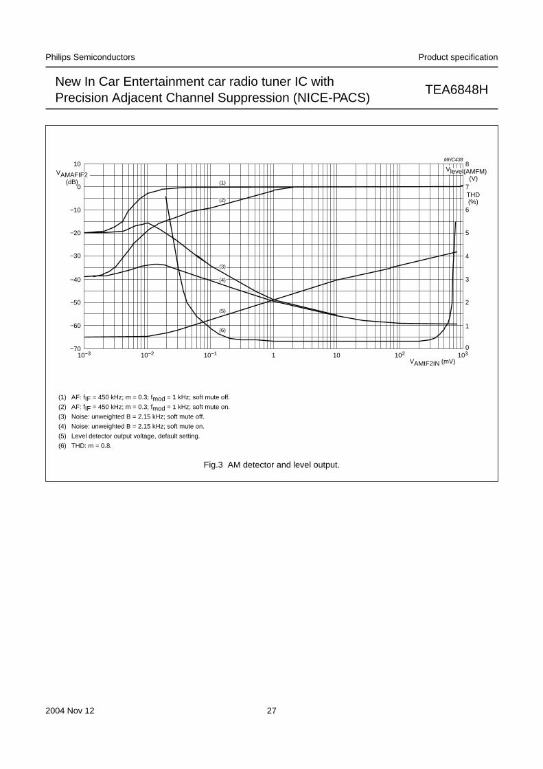
Fig.4 AM level voltage.
(1) Level DAA setting byte 5 = FFH.
(2) Level DAA setting byte 5 = 84H (standard setting).
(3) Level DAA setting byte 5 = 00H.
handbook, full pagewidth
MHC440
1 kΩ
1 kΩ
100 Ω
50 Ω
100 Ω
70
71
73
77
7814
VIFAMPIN
18
oscilloscope,counter
8.5 V
8.5 V
test signal
4.7 nF
19
TEA6848H
Vlevel(AMFM)
Trep
VXTAL2
Vpulse
Vpulse
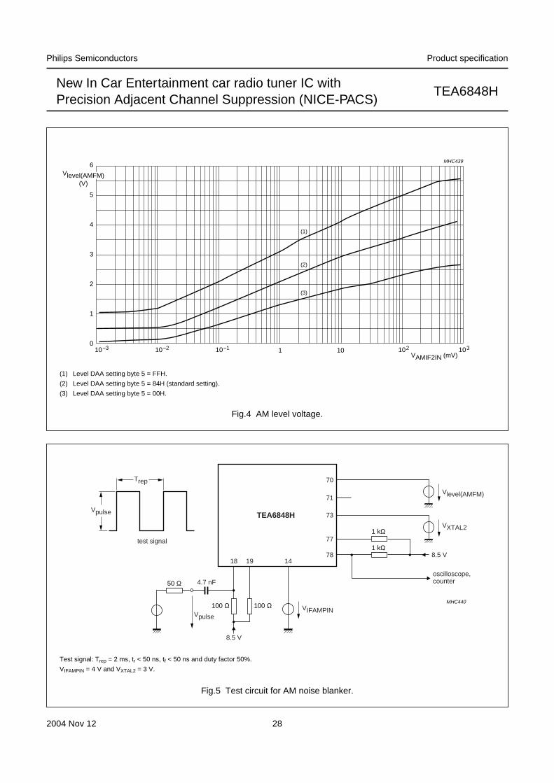
Fig.5 Test circuit for AM noise blanker.
Test signal: Trep = 2 ms, tr < 50 ns, tf < 50 ns and duty factor 50%.
VIFAMPIN = 4 V and VXTAL2 = 3 V.

2004 Nov 12 29
Philips Semiconductors Product specification
New In Car Entertainment car radio tuner IC withPrecision Adjacent Channel Suppression (NICE-PACS)
TEA6848H
handbook, full pagewidth6
0
2
1
3
5
4
MHC441
10−3 10−2 10−1 1 10VFMMIX2IN (mV)
102 103
(2)
(3)
Vlevel(AMFM)(V)
(1)
Fig.6 FM level voltage.
(1) Level DAA setting byte 5 = FFH.
(2) Level DAA setting byte 5 = 84H (standard setting).
(3) Level DAA setting byte 5 = 00H.
2004 Nov 12 30
Philips Semiconductors Product specification
New In Car Entertainment car radio tuner IC withPrecision Adjacent Channel Suppression (NICE-PACS)
TEA6848H
handbook, full pagewidth10
0
−80
−70
−60
−50
−40
−30
−20
−10
MHC442
10−3 10−2 10−1
VFMMIX2IN (mV)1 10 102 103
VFMMPX;VRDSMPX
(dB)
(2)
(1)
(4)
(3)
6
7
THD(%)
8
9
0
2
1
3
5
4
(5)
Vlevel(AMFM) (V)
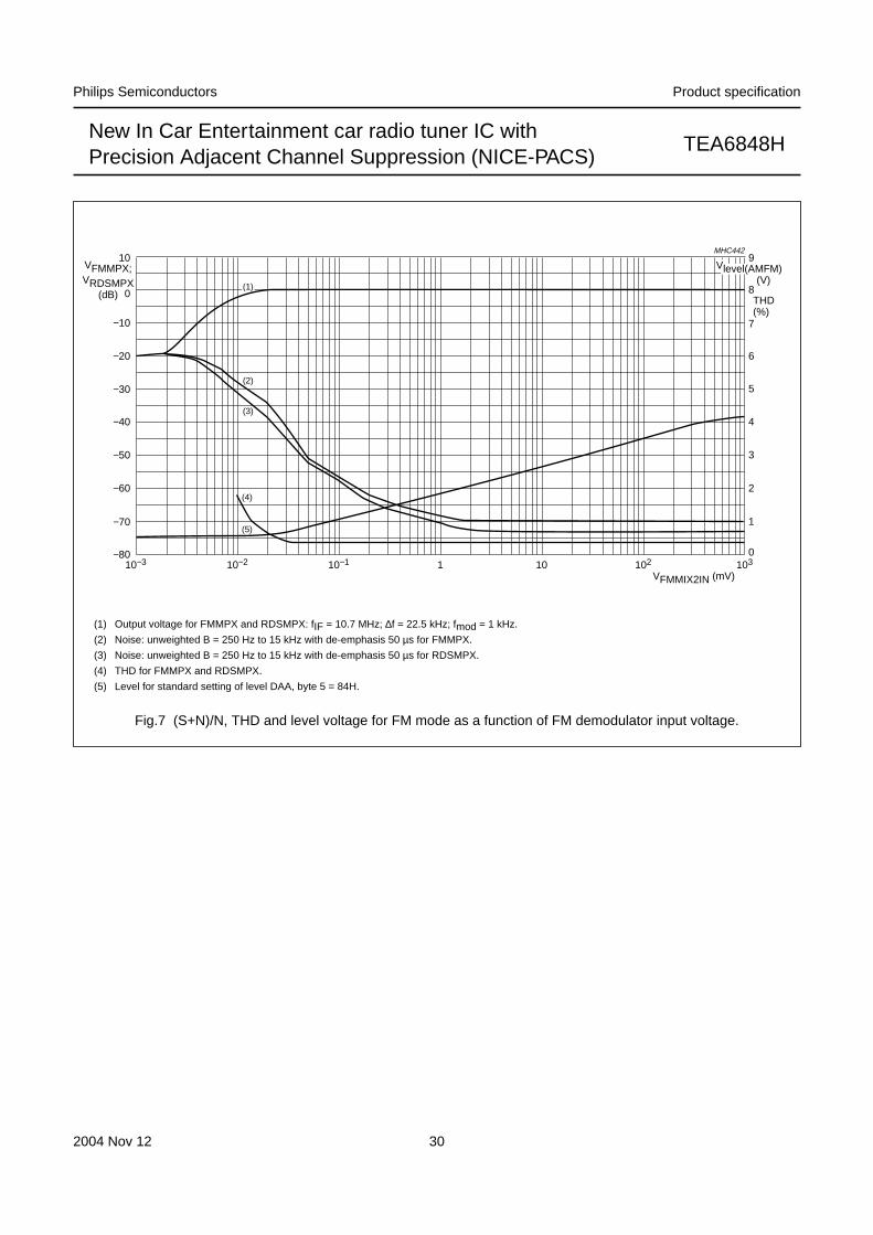
Fig.7 (S+N)/N, THD and level voltage for FM mode as a function of FM demodulator input voltage.
(1) Output voltage for FMMPX and RDSMPX: fIF = 10.7 MHz; ∆f = 22.5 kHz; fmod = 1 kHz.
(2) Noise: unweighted B = 250 Hz to 15 kHz with de-emphasis 50 µs for FMMPX.
(3) Noise: unweighted B = 250 Hz to 15 kHz with de-emphasis 50 µs for RDSMPX.
(4) THD for FMMPX and RDSMPX.
(5) Level for standard setting of level DAA, byte 5 = 84H.
2004 Nov 12 31
Philips Semiconductors Product specification
New In Car Entertainment car radio tuner IC withPrecision Adjacent Channel Suppression (NICE-PACS)
TEA6848H
12 I2C-BUS PROTOCOL
12.1 I2C-bus specification
Information about the I2C-bus can be found in the brochure“The I2C-bus and how to use it” (order number9398 393 40011).
The standard I2C-bus specification is expanded by thefollowing definitions.
IC addresses:
• 1st IC address C2H: 1100001 R/W
• 2nd IC address C0H: 1100000 R/W.
Structure of the I2C-bus logic: slave transceiver with autoincrement.
Subaddresses are not used.
A second I2C-bus address can be selected by connectingpin FREF via a 68 kΩ resistor to GND.
12.1.1 DATA TRANSFER
Data sequence: address, byte 0, byte 1, byte 2, byte 3,byte 4, byte 5, byte 6, and byte 7. The data transfer has tobe in this order. The LSB = 0 indicates a WRITE operationto the TEA6848H.
Bit 7 of each byte is considered the MSB and has to betransferred as the first bit of the byte.
The data becomes valid at the output of the internallatches with the acknowledge of each byte. A STOPcondition after any byte can shorten transmission times.
When writing to the transceiver by using the STOPcondition before completion of the whole transfer:
• The remaining bytes will contain the old information
• If the transfer of a byte is not completed, this byte is lostand the previous information is available.
12.1.2 I2C-BUS PULL-UP RESISTORS
When the IC is used together with the TEA688x orTEF689x and both SCL and SDA lines are connected viathe I2C-bus to the TEA688x or TEF689x, the pull-upresistors of the tuner IC should be connected to the digitalsupply voltage of the TEA688x or TEF689x. Otherwise anI2C-bus pull-down can occur switching off the tuner ICsupply when the I2C-bus buffer interface of the TEA688xor TEF689x is enabled for data transfer to the tuner IC.
12.1.3 FREQUENCY SETTING
For new frequency setting, in both AM and FM mode, theprogrammable divider is enabled by setting bit MUTE = 1.To select an FM frequency, two I2C-bus transmissions arenecessary:
• First: bit MUTE = 1
• Second: bit MUTE = 0.
12.1.4 DEFAULT SETTINGS
No default settings at power-on reset. One I2C-bustransmission is required to program the IC.
12.1.5 TIMING REQUIREMENTS
Table 1 Timing requirements of I2C-bus software
FUNCTION TIMING
Switching fromFM to AM
400 ms (10 µF at pin CAGC)
Switching fromAM to FM
100 ms (10 µF at pin CAGC; widebandposition has to be set for at least100 ms to activate speed-up circuitry)
Start-up in FMmode
wideband position has to be set for atleast 100 ms to activate speed-upcircuitry
Switching todynamic mode
500 µs (18 nF at pin TACD; widebandposition has to be set for at least500 µs to activate clamping circuitry atpin TACD)

2004 Nov 12 32
Philips Semiconductors Product specification
New In Car Entertainment car radio tuner IC withPrecision Adjacent Channel Suppression (NICE-PACS)
TEA6848H
12.2 I2C-bus protocol
12.2.1 DATA TRANSFER MODE AND IC ADDRESS
Table 2 Write mode
Notes
1. S = START condition.
2. A = acknowledge.
3. P = STOP condition.
Table 3 Read mode
Notes
1. S = START condition.
2. A = acknowledge.
Table 4 IC address byte
Notes
1. Defined by address pin FREF:
a) 1 = 1st IC address
b) 0 = 2nd IC address.
2. Read or write mode:
a) 0 = write operation to TEA6848H
b) 1 = read operation from TEA6848H.
12.2.2 WRITE MODE: DATA BYTE 0
Table 5 Format of data byte 0
Table 6 Description of data byte 0 bits
S(1) address (write) A(2) data byte(s) A(2) P(3)
S(1) address (read) A(2) data byte 1
IC ADDRESS MODE
1 1 0 0 0 0 0/1(1) R/W(2)
BIT 7 BIT 6 BIT 5 BIT 4 BIT 3 BIT 2 BIT 1 BIT 0
AF PLL14 PLL13 PLL12 PLL11 PLL10 PLL9 PLL8
BIT SYMBOL DESCRIPTION
7 AF Alternative frequency. If AF = 0, then normal operation. If AF = 1, then AF (RDS)update mode.
6 to 0 PLL[14:8] Setting of programmable counter of synthesizer PLL. Upper byte of PLL dividerword.
2004 Nov 12 33
Philips Semiconductors Product specification
New In Car Entertainment car radio tuner IC withPrecision Adjacent Channel Suppression (NICE-PACS)
TEA6848H
12.2.3 WRITE MODE: DATA BYTE 1
Table 7 Format of data byte 1
Table 8 Description of data byte 1 bits
12.2.4 WRITE MODE: DATA BYTE 2
Table 9 Format of data byte 2
Table 10 Description of data byte 2 bits
12.2.5 WRITE MODE: DATA BYTE 3
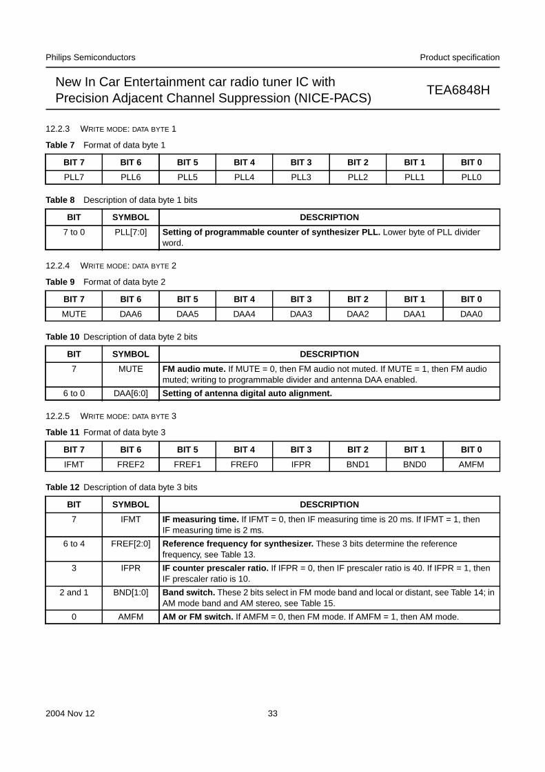
Table 11 Format of data byte 3
Table 12 Description of data byte 3 bits
BIT 7 BIT 6 BIT 5 BIT 4 BIT 3 BIT 2 BIT 1 BIT 0
PLL7 PLL6 PLL5 PLL4 PLL3 PLL2 PLL1 PLL0
BIT SYMBOL DESCRIPTION
7 to 0 PLL[7:0] Setting of programmable counter of synthesizer PLL. Lower byte of PLL dividerword.
BIT 7 BIT 6 BIT 5 BIT 4 BIT 3 BIT 2 BIT 1 BIT 0
MUTE DAA6 DAA5 DAA4 DAA3 DAA2 DAA1 DAA0
BIT SYMBOL DESCRIPTION
7 MUTE FM audio mute. If MUTE = 0, then FM audio not muted. If MUTE = 1, then FM audiomuted; writing to programmable divider and antenna DAA enabled.
6 to 0 DAA[6:0] Setting of antenna digital auto alignment.
BIT 7 BIT 6 BIT 5 BIT 4 BIT 3 BIT 2 BIT 1 BIT 0
IFMT FREF2 FREF1 FREF0 IFPR BND1 BND0 AMFM
BIT SYMBOL DESCRIPTION
7 IFMT IF measuring time. If IFMT = 0, then IF measuring time is 20 ms. If IFMT = 1, thenIF measuring time is 2 ms.
6 to 4 FREF[2:0] Reference frequency for synthesizer. These 3 bits determine the referencefrequency, see Table 13.
3 IFPR IF counter prescaler ratio. If IFPR = 0, then IF prescaler ratio is 40. If IFPR = 1, thenIF prescaler ratio is 10.
2 and 1 BND[1:0] Band switch. These 2 bits select in FM mode band and local or distant, see Table 14; inAM mode band and AM stereo, see Table 15.
0 AMFM AM or FM switch. If AMFM = 0, then FM mode. If AMFM = 1, then AM mode.
2004 Nov 12 34
Philips Semiconductors Product specification
New In Car Entertainment car radio tuner IC withPrecision Adjacent Channel Suppression (NICE-PACS)
TEA6848H
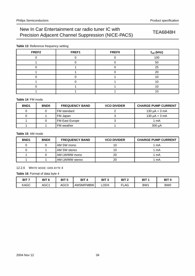
Table 13 Reference frequency setting
Table 14 FM mode
Table 15 AM mode
12.2.6 WRITE MODE: DATA BYTE 4
Table 16 Format of data byte 4
FREF2 FREF1 FREF0 fref (kHz)
0 0 0 100
1 0 0 50
0 1 0 25
1 1 0 20
0 0 1 10
1 0 1 10
0 1 1 10
1 1 1 10
BND1 BND0 FREQUENCY BAND VCO DIVIDER CHARGE PUMP CURRENT
0 0 FM standard 2 130 µA + 3 mA
0 1 FM Japan 3 130 µA + 3 mA
1 0 FM East Europe 3 1 mA
1 1 FM weather 1 300 µA
BND1 BND0 FREQUENCY BAND VCO DIVIDER CHARGE PUMP CURRENT
0 0 AM SW mono 10 1 mA
0 1 AM SW stereo 10 1 mA
1 0 AM LW/MW mono 20 1 mA
1 1 AM LW/MW stereo 20 1 mA
BIT 7 BIT 6 BIT 5 BIT 4 BIT 3 BIT 2 BIT 1 BIT 0
KAGC AGC1 AGC0 AMSM/FMBW LODX FLAG BW1 BW0
2004 Nov 12 35
Philips Semiconductors Product specification
New In Car Entertainment car radio tuner IC withPrecision Adjacent Channel Suppression (NICE-PACS)
TEA6848H
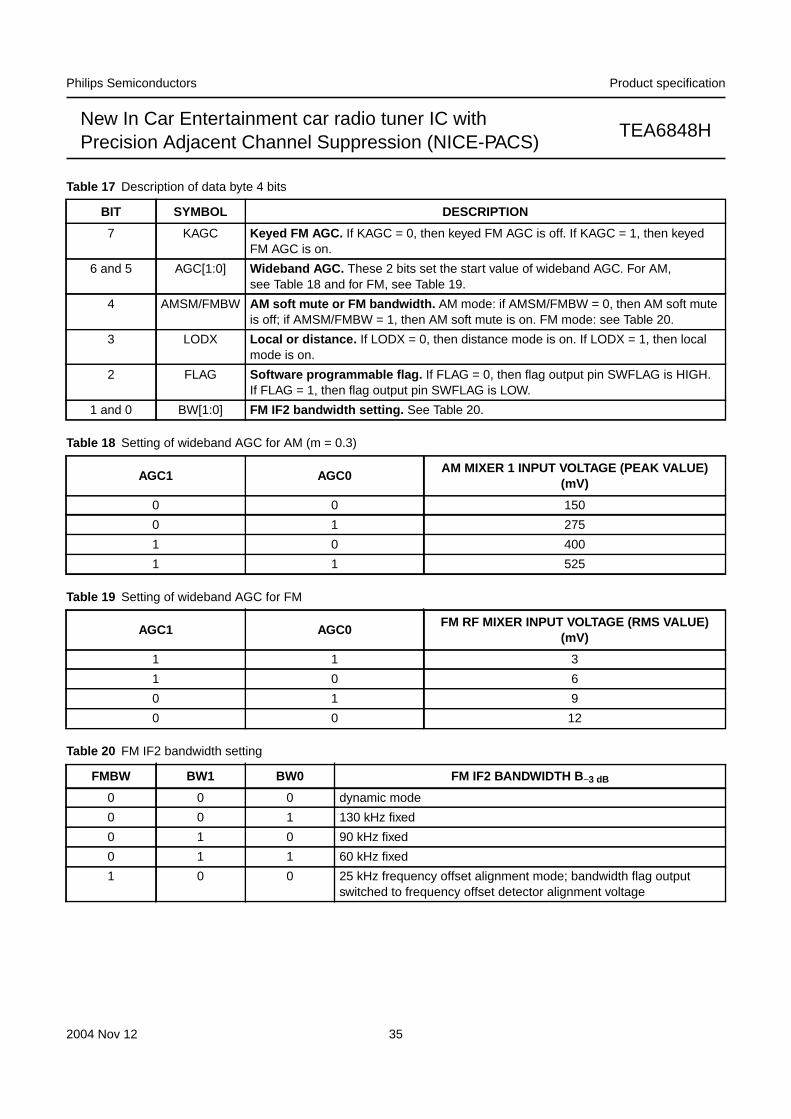
Table 17 Description of data byte 4 bits
Table 18 Setting of wideband AGC for AM (m = 0.3)
Table 19 Setting of wideband AGC for FM
Table 20 FM IF2 bandwidth setting
BIT SYMBOL DESCRIPTION
7 KAGC Keyed FM AGC. If KAGC = 0, then keyed FM AGC is off. If KAGC = 1, then keyedFM AGC is on.
6 and 5 AGC[1:0] Wideband AGC. These 2 bits set the start value of wideband AGC. For AM,see Table 18 and for FM, see Table 19.
4 AMSM/FMBW AM soft mute or FM bandwidth. AM mode: if AMSM/FMBW = 0, then AM soft muteis off; if AMSM/FMBW = 1, then AM soft mute is on. FM mode: see Table 20.
3 LODX Local or distance. If LODX = 0, then distance mode is on. If LODX = 1, then localmode is on.
2 FLAG Software programmable flag. If FLAG = 0, then flag output pin SWFLAG is HIGH.If FLAG = 1, then flag output pin SWFLAG is LOW.
1 and 0 BW[1:0] FM IF2 bandwidth setting. See Table 20.
AGC1 AGC0AM MIXER 1 INPUT VOLTAGE (PEAK VALUE)
(mV)
0 0 150
0 1 275
1 0 400
1 1 525
AGC1 AGC0FM RF MIXER INPUT VOLTAGE (RMS VALUE)
(mV)
1 1 3
1 0 6
0 1 9
0 0 12
FMBW BW1 BW0 FM IF2 BANDWIDTH B −3 dB
0 0 0 dynamic mode
0 0 1 130 kHz fixed
0 1 0 90 kHz fixed
0 1 1 60 kHz fixed
1 0 0 25 kHz frequency offset alignment mode; bandwidth flag outputswitched to frequency offset detector alignment voltage
2004 Nov 12 36
Philips Semiconductors Product specification
New In Car Entertainment car radio tuner IC withPrecision Adjacent Channel Suppression (NICE-PACS)
TEA6848H
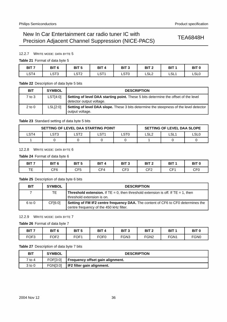
12.2.7 WRITE MODE: DATA BYTE 5
Table 21 Format of data byte 5
Table 22 Description of data byte 5 bits
Table 23 Standard setting of data byte 5 bits
12.2.8 WRITE MODE: DATA BYTE 6
Table 24 Format of data byte 6
Table 25 Description of data byte 6 bits
12.2.9 WRITE MODE: DATA BYTE 7
Table 26 Format of data byte 7
Table 27 Description of data byte 7 bits
BIT 7 BIT 6 BIT 5 BIT 4 BIT 3 BIT 2 BIT 1 BIT 0
LST4 LST3 LST2 LST1 LST0 LSL2 LSL1 LSL0
BIT SYMBOL DESCRIPTION
7 to 3 LST[4:0] Setting of level DAA starting point. These 5 bits determine the offset of the leveldetector output voltage.
2 to 0 LSL[2:0] Setting of level DAA slope. These 3 bits determine the steepness of the level detectoroutput voltage.
SETTING OF LEVEL DAA STARTING POINT SETTING OF LEVEL DAA SLOPE
LST4 LST3 LST2 LST1 LST0 LSL2 LSL1 LSL0
1 0 0 0 0 1 0 0
BIT 7 BIT 6 BIT 5 BIT 4 BIT 3 BIT 2 BIT 1 BIT 0
TE CF6 CF5 CF4 CF3 CF2 CF1 CF0
BIT SYMBOL DESCRIPTION
7 TE Threshold extension. If TE = 0, then threshold extension is off. If TE = 1, thenthreshold extension is on.
6 to 0 CF[6:0] Setting of FM IF2 centre frequency DAA. The content of CF6 to CF0 determines thecentre frequency of the 450 kHz filter.
BIT 7 BIT 6 BIT 5 BIT 4 BIT 3 BIT 2 BIT 1 BIT 0
FOF3 FOF2 FOF1 FOF0 FGN3 FGN2 FGN1 FGN0
BIT SYMBOL DESCRIPTION
7 to 4 FOF[3:0] Frequency offset gain alignment.
3 to 0 FGN[3:0] IF2 filter gain alignment.

2004 Nov 12 37
Philips Semiconductors Product specification
New In Car Entertainment car radio tuner IC withPrecision Adjacent Channel Suppression (NICE-PACS)
TEA6848H
12.2.10 READ MODE: DATA BYTE 0
Table 28 Format of 1st data byte
Table 29 Description of data byte 0 bits
13 TEST AND APPLICATION INFORMATION
Table 30 List of components for test and application circuits (Figs 8, 9, 10 and 11)
BIT 7 BIT 6 BIT 5 BIT 4 BIT 3 BIT 2 BIT 1 BIT 0
IFC7 IFC6 IFC5 IFC4 IFC3 IFC2 IFC1 IFC0
BIT SYMBOL DESCRIPTION
7 to 0 IFC[7:0] IF counter result. These bits contain the least significant eight bits of the IF counterresult.
SYMBOL PARAMETER TYPE MANUFACTURER
C1 capacitor for VCO tuning 270 pF; type NP0 −L1 10.7 MHz IF coil P7 PSG P826RC 5134N=S TOKO
L2 450 kHz IF coil P7PSGAE-5078D=S TOKO
L3 oscillator coil E543SNAS-02010 TOKO
L4 FM image rejection 611SNS-1066Y TOKO
L5 FM input transformer 369INS-3076X TOKO
L6 FM antenna coil LQN1HR50; 215 nH MURATA
L7 PIN diode bias LQN1HR21; 500 nH MURATA
L8 connection image reject wire 10 mm/printed coil −L9 AM input 388BN-1211Z TOKO
R4 resistor for stabilizer 3.3 kΩ; RC12G BC Components
− crystal 20.5 MHz LN-G102-587 NDK
2004 Nov 12 38
Philips Semiconductors Product specification
New In Car Entertainment car radio tuner IC withPrecision Adjacent Channel Suppression (NICE-PACS)
TEA6848H
handbook, full pagewidth
DAA
VCO
AMMIXER 1
AMMIXER 2
AM
AGC
90°
FMI/Q MIXER 1
FMAGC
TUNING SYSTEM
AM-NOISEDETECTOR
PEAK/AVERAGE
BLANKPULSE
÷10/÷20
÷1/ ÷2/÷3
90°
TEA6848H
FMMIXER 2
÷2
19 18 15 14 13 12 11 10 9 8 7 6 520
22
23
24
25
26
27
28
29
30
3132
3334
35
36
37
38
39
40 41 42 43 44 45 46 47 48 49 50 51
AM
LEVEL
LEVEL
BB156
Vtune
frefPLL
DGND
22 Ω
1nF
C14.7 kΩ
100 nF
10 kΩ
2.2 kΩ
1.2 kΩ3.9nF
100 nF1.8pF
2.7pF
22Ω
22nF
L33.3nF
SFE 10.7MS322
Ω22 nF
L1 SFE 10.7MS3
WB/JAPAN/OIRT
21
SW CONTROLFLAG
17 16
47µF
100nF
220nF22
nF
22Ω
22nF
22 nF
22Ω
22 nF
VDDD
ANTENNA
RFGND
4:6
22Ω
L5
BB814
22 kΩ
L4
BAS16
WB FLAG
BAV99
10 nF
1 nF
270 Ω
BAQ806
220nF
antenna
2.2 MΩ
5 V
L8
18 pF
215nH
6.8 pF1pF
12pF
500 nH
1nF
10µF
1nF
1nF
2.2kΩ
330Ω
BA595
100 nF
22 Ω
220nF
BC847C
1.8 MΩ
150pF
820µH
560Ω
2.2 nF
56µH
470µH
100 nF
BF862
2.2MΩ
10 nF
6.8µH
1 µF
1 µF
L9
10kΩ
22 nF
22 µF
220 nF
270pF
100 kΩ
L7
L6
+
++
I2C-bus
I2C-bus
I2C-bus
I2C-bus
I2C-bus
+
+
×
×
×
×
MHC443
A
B
C
D
E
F
G
H
I
L
M
N
K
J
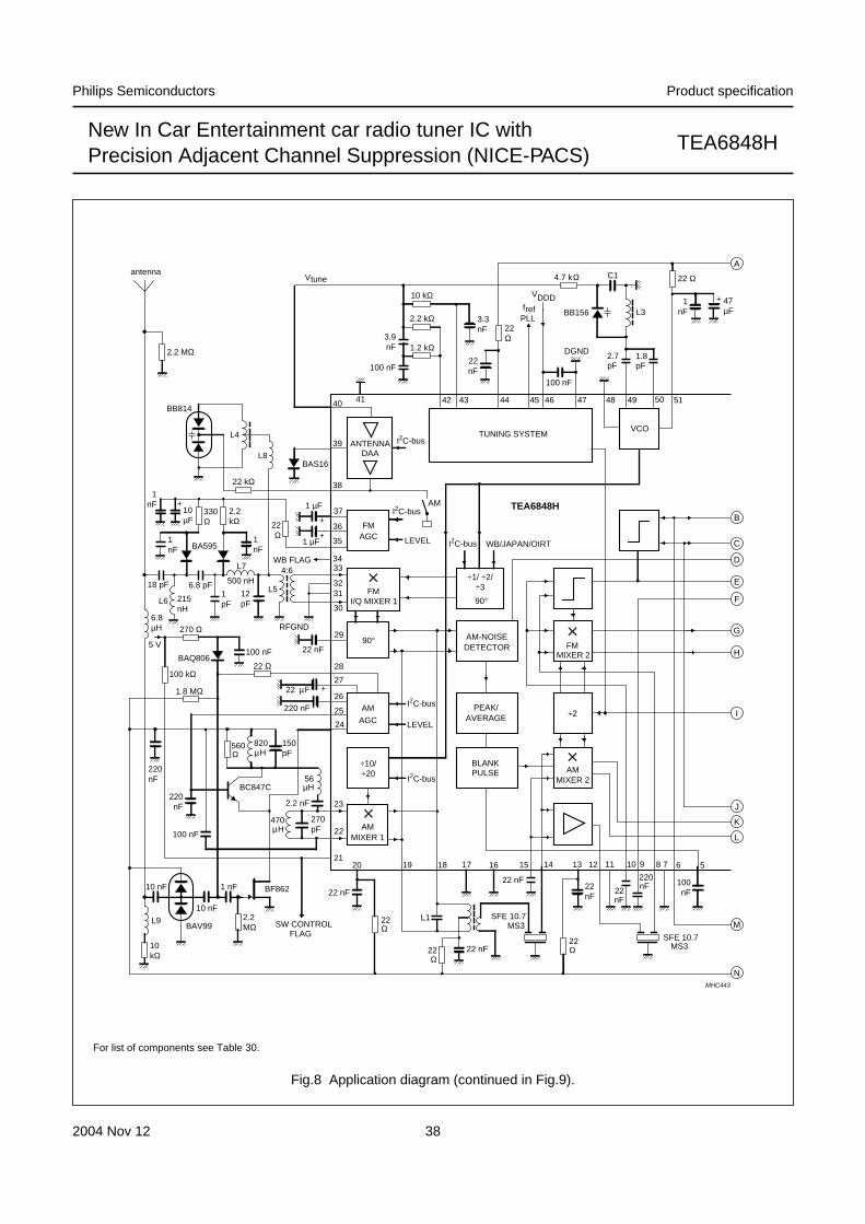
Fig.8 Application diagram (continued in Fig.9).
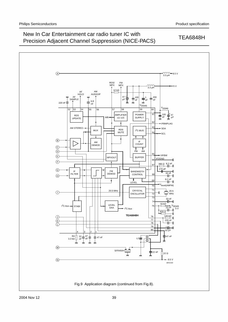
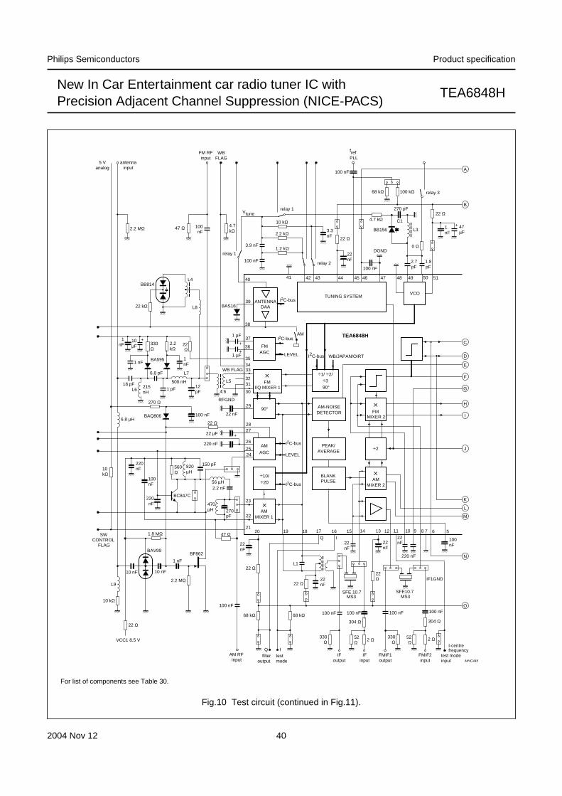
For list of components see Table 30.
2004 Nov 12 39
Philips Semiconductors Product specification
New In Car Entertainment car radio tuner IC withPrecision Adjacent Channel Suppression (NICE-PACS)
TEA6848H
handbook, full pagewidth
RDSUPDATE
CRYSTALOSCILLATOR
POWERSUPPLY
LEVELDAA
IFCOUNT
AMDEMOD
MUX
IFFILTER
FMDEMOD
STABI
BUFFER
BANDWIDTHCONTROL
x1/ x15AMPLIFIER
MPXOUT
20.5 MHz
4 3 2 1
52 53 54 55 56 57 58 59 60
61
62
63
64
65
66
67
68
69
70
71
72
73
74
75
76
77
78
79
80
WB
LEVEL
FM AM
SAMPLEAF
HOLDAF
5 V
AUDIO/IFAM
RDS/MPX MPX
FM
3.3 µH
3.3 µH
100nF
100nF
8.5 V
IFBWFLAG
SCL
SDA
VIFBW
Vlevel(AMFM)
20.5MHz
22 Ω22 nF
L2
SFR450H
8.5 V
IF2GND
VDDA55 V
220 nF6.8nF
12 kΩ
47µF
1nF
200nF
47µF
390 Ω 8.2 nF
33 nF
8.2 nF
33 nF
10 kΩ
820 Ω
120 kΩ
22 nF
10 µF
220 nF
47 nF4747 nFnF
22nF
R43.3 kΩ
VDDA6
VDDA5
AM STEREO
MUTERDS
270 pF
I2C-bus
I2C-BUS
I2C-bus
+
+
+
MHC444
A
B
C
D
E
F
G
H
I
L
M
N
K
JTEA6848H
Fig.9 Application diagram (continued from Fig.8).
2004 Nov 12 40
Philips Semiconductors Product specification
New In Car Entertainment car radio tuner IC withPrecision Adjacent Channel Suppression (NICE-PACS)
TEA6848H
handbook, full pagewidth
DAA
VCO
AMMIXER 1
AMMIXER 2
AM
AGC
90°
FMI/Q MIXER 1
FMAGC
TUNING SYSTEM
AM-NOISEDETECTOR
PEAK/AVERAGE
BLANKPULSE
÷10/÷20
÷1/ ÷2/÷3
90°
TEA6848H
FMMIXER 2
÷2
19 18 15 14 13 12 11 10 9 8 7 6 520
22
23
2425
26
2728
29
30
3132
333435
36
37
38
39
40 41 42 43 44 45 46 47 48 49 50 51
AM
LEVEL
LEVEL
WB/JAPAN/OIRT
2117 16
ANTENNA
I2C-bus
I2C-bus
I2C-bus
I2C-bus
I2C-bus
×
×
×
×
MHC445
A
B
C
D
E
F
G
H
I
L
M
N
O
K
J
BB156
Vtune
DGND
22 Ω4.7 kΩ
22 Ω
1.2 kΩ
2.2 kΩ
10 kΩ4.7kΩ
0 Ω
1nF
270 pF
100 nF
3.9 nF
100 nF 1.8pF
2.7pF
22nF
L3
C1
3.3nF
SFE10.7MS3
I-centre
test modefrequency
22nF
L1
SFE 10.7MS3
filter
Q I
IF1GND
47µF
100nF
220 nF
22Ω
22nF
22nF22
nF22nF
frefPLL
100 nF 100 nF 100 nF 100 nF
2 Ω2 Ω
304 Ω304 Ω
52Ω
52Ω
330Ω
330Ω
AM RF FMIF1output
IFoutput
FMIF2input
IFinput
100 nF
100 kΩ68 kΩ relay 3
relay 2
relay 1
relay 1
RFGND
4:6
L5
BB814L4
L8 BAS16
WB FLAG
antennainput
FM RFinput
100nF
WBFLAG
1 µF
1 µF
10kΩ
VCC1 8.5 V
5 Vanalog
BAV99
10 nF
1 nF
270 Ω
22 ΩBAQ806
220nF
SW
FLAG
100 nF
220nF
BC847C
1.8 MΩ
2.2 MΩ
10 kΩ
22 Ω
68 kΩ
22 Ω
22 Ω
68 kΩ
150 pF820µH
56 µH
470µH
560Ω
47 Ω
2.2 nF
BF862
10 nF
L9
22 nF
22 µF
220 nF
270pF
CONTROL
18 pF215nH
6.8 pF
1 pF12pF
500 nH
1nF
10µF
1nF1 nF
2.2kΩ
330Ω
22Ω
BA595
L7
L6
6.8 µH
100nF
100 nF
Q I
+ ++
+
input outputtestmode input
+2.2 MΩ
22 kΩ
47 Ω
Fig.10 Test circuit (continued in Fig.11).
For list of components see Table 30.
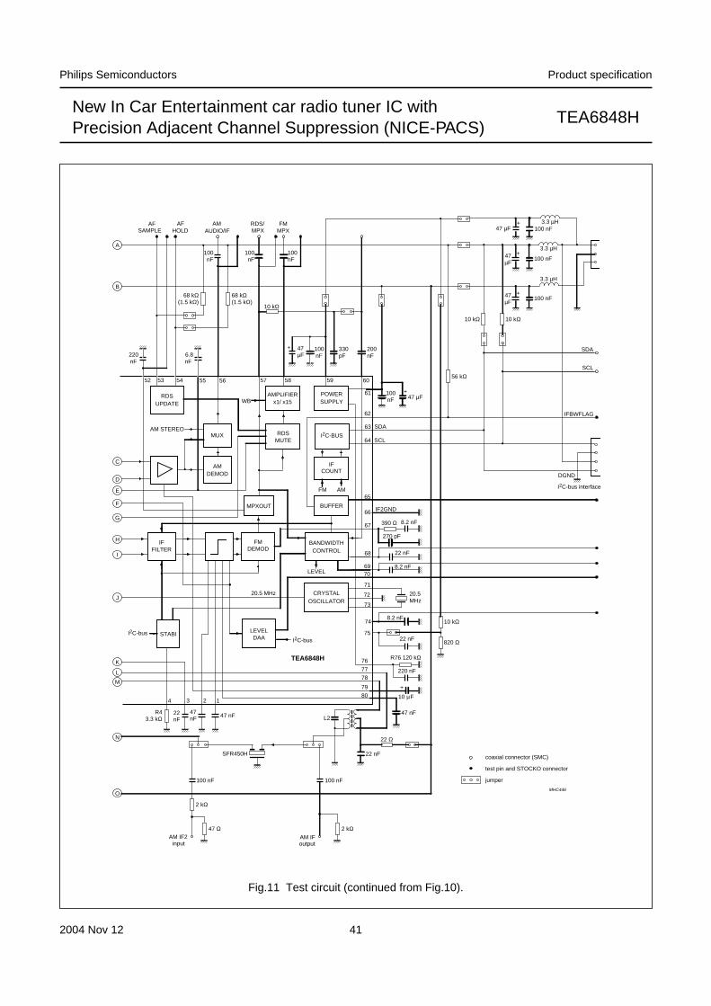
2004 Nov 12 41
Philips Semiconductors Product specification
New In Car Entertainment car radio tuner IC withPrecision Adjacent Channel Suppression (NICE-PACS)
TEA6848H
handbook, full pagewidth
RDSUPDATE
CRYSTALOSCILLATOR
POWERSUPPLY
LEVELDAA
IFCOUNT
AMDEMOD
MUX
IFFILTER
FMDEMOD
STABI
BUFFER
BANDWIDTHCONTROL
x1/ x15AMPLIFIER
MPXOUT
20.5 MHz
4 3 2 1
52 53 54 55 56 57 58 59 60
61
62
63
64
65
66
67
68
6970
71
72
73
74
75
76
77
78
79
80
WB
LEVEL
FM AM
IFBWFLAG
SCL
SDA
20.5MHz
22 Ω
22 nF
L2
100 nF jumper
test pin and STOCKO connector
coaxial connector (SMC)
100 nF
2 kΩ
47 Ω
SFR450H
IF2GND
390 Ω 8.2 nF
22 nF
22 nF
8.2 nF
8.2 nF
R76 120 kΩ
10 µF
220 nF
47 nF4747 nFnF
22nF
R43.3 kΩ
AM STEREO
MUTERDS
270 pF
I2C-bus
I2C-BUS
I2C-bus
+
+
MHC446
68 kΩ(1.5 kΩ)
100nF
100nF
100nF
68 kΩ(1.5 kΩ)
10 kΩ
10 kΩ
56 kΩ
10 kΩ
820 Ω
10 kΩ
47µF
47 µF
220nF
6.8nF
100nF
100nF
47µF
47µF
47 µF3.3 µH
3.3 µH
3.3 µH
100 nF
100 nF
100 nF
SDA
SCL
DGND
I2C-bus interface
330pF
200nF
2 kΩ
B
A
C
D
E
F
G
H
I
J
M
N
O
L
K
AM IF2 AM IFoutputinput
SAMPLEAF
HOLDAF
AUDIO/IFAM RDS/
MPX MPXFM
+
+
+
+
TEA6848H
Fig.11 Test circuit (continued from Fig.10).
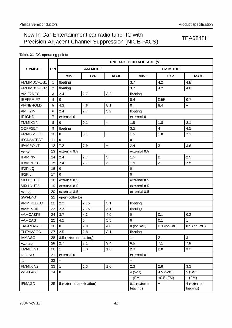
2004 Nov 12 42
Philips Semiconductors Product specification
New In Car Entertainment car radio tuner IC withPrecision Adjacent Channel Suppression (NICE-PACS)
TEA6848H
Table 31 DC operating points
SYMBOL PIN
UNLOADED DC VOLTAGE (V)
AM MODE FM MODE
MIN. TYP. MAX. MIN. TYP. MAX.
FMLIMDCFDB1 1 floating 3.7 4.2 4.8
FMLIMDCFDB2 2 floating 3.7 4.2 4.8
AMIF2DEC 3 2.4 2.7 3.2 floating
IREFFMIF2 4 0 0.4 0.55 0.7
AMNBHOLD 5 4.3 4.6 5.1 8 8.4 −AMIF2IN 6 2.4 2.7 3.2 floating
IF1GND 7 external 0 external 0
FMMIX2IN 8 0 0.1 − 1.5 1.8 2.1
COFFSET 9 floating 3.5 4 4.5
FMMIX2DEC 10 0 0.1 − 1.5 1.8 2.1
IFCDAATEST 11 0 0
IFAMPOUT 12 7.2 7.9 − 2.4 3 3.6
VDDA1 13 external 8.5 external 8.5
IFAMPIN 14 2.4 2.7 3 1.5 2 2.5
IFAMPDEC 15 2.4 2.7 3 1.5 2 2.5
IF2FILQ 16 0 0
IF2FILI 17 0 0
MIX1OUT1 18 external 8.5 external 8.5
MIX1OUT2 19 external 8.5 external 8.5
VDDA2 20 external 8.5 external 8.5
SWFLAG 21 open-collector
AMMIX1DEC 22 2.3 2.75 3.1 floating
AMMIX1IN 23 2.3 2.75 3.1 floating
VAMCASFB 24 3.7 4.3 4.9 0 0.1 0.2
VAMCAS 25 4.5 5 5.5 0 0.1 1
TAFAMAGC 26 0 2.8 4.6 0 (no WB) 0.3 (no WB) 0.5 (no WB)
THFAMAGC 27 2.5 2.8 3.1 floating
IAMAGC 28 8.5 (external biasing) 1 2 3
Vref(MIX) 29 2.7 3.1 3.4 6.5 7.1 7.9
FMMIXIN1 30 1 1.3 1.6 2.3 2.8 3.3
RFGND 31 external 0 external 0
i.c. 32 − −FMMIXIN2 33 1 1.3 1.6 2.3 2.8 3.3
WBFLAG 34 0 4 (WB) 4.5 (WB) 5 (WB)
− (FM) <0.5 (FM) − (FM)
IFMAGC 35 5 (external application) 0.1 (externalbiasing)
− 4 (externalbiasing)
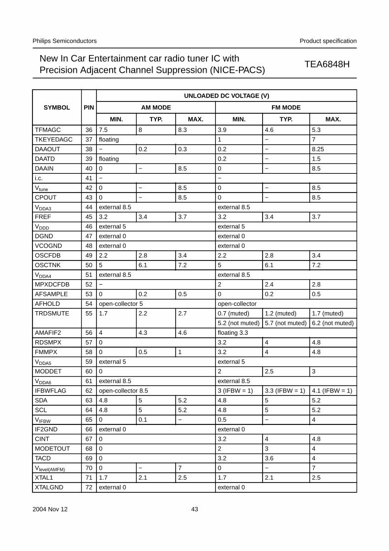
2004 Nov 12 43
Philips Semiconductors Product specification
New In Car Entertainment car radio tuner IC withPrecision Adjacent Channel Suppression (NICE-PACS)
TEA6848H
TFMAGC 36 7.5 8 8.3 3.9 4.6 5.3
TKEYEDAGC 37 floating 1 − 7
DAAOUT 38 − 0.2 0.3 0.2 − 8.25
DAATD 39 floating 0.2 − 1.5
DAAIN 40 0 − 8.5 0 − 8.5
i.c. 41 − −Vtune 42 0 − 8.5 0 − 8.5
CPOUT 43 0 − 8.5 0 − 8.5
VDDA3 44 external 8.5 external 8.5
FREF 45 3.2 3.4 3.7 3.2 3.4 3.7
VDDD 46 external 5 external 5
DGND 47 external 0 external 0
VCOGND 48 external 0 external 0
OSCFDB 49 2.2 2.8 3.4 2.2 2.8 3.4
OSCTNK 50 5 6.1 7.2 5 6.1 7.2
VDDA4 51 external 8.5 external 8.5
MPXDCFDB 52 − 2 2.4 2.8
AFSAMPLE 53 0 0.2 0.5 0 0.2 0.5
AFHOLD 54 open-collector 5 open-collector
TRDSMUTE 55 1.7 2.2 2.7 0.7 (muted) 1.2 (muted) 1.7 (muted)
5.2 (not muted) 5.7 (not muted) 6.2 (not muted)
AMAFIF2 56 4 4.3 4.6 floating 3.3
RDSMPX 57 0 3.2 4 4.8
FMMPX 58 0 0.5 1 3.2 4 4.8
VDDA5 59 external 5 external 5
MODDET 60 0 2 2.5 3
VDDA6 61 external 8.5 external 8.5
IFBWFLAG 62 open-collector 8.5 3 (IFBW = 1) 3.3 (IFBW = 1) 4.1 (IFBW = 1)
SDA 63 4.8 5 5.2 4.8 5 5.2
SCL 64 4.8 5 5.2 4.8 5 5.2
VIFBW 65 0 0.1 − 0.5 − 4
IF2GND 66 external 0 external 0
CINT 67 0 3.2 4 4.8
MODETOUT 68 0 2 3 4
TACD 69 0 3.2 3.6 4
Vlevel(AMFM) 70 0 − 7 0 − 7
XTAL1 71 1.7 2.1 2.5 1.7 2.1 2.5
XTALGND 72 external 0 external 0
SYMBOL PIN
UNLOADED DC VOLTAGE (V)
AM MODE FM MODE
MIN. TYP. MAX. MIN. TYP. MAX.
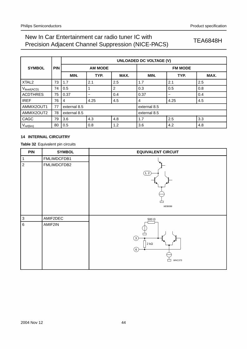
2004 Nov 12 44
Philips Semiconductors Product specification
New In Car Entertainment car radio tuner IC withPrecision Adjacent Channel Suppression (NICE-PACS)
TEA6848H
14 INTERNAL CIRCUITRY
Table 32 Equivalent pin circuits
XTAL2 73 1.7 2.1 2.5 1.7 2.1 2.5
Vlevel(ACD) 74 0.5 1 2 0.3 0.5 0.8
ACDTHRES 75 0.37 − 0.4 0.37 − 0.4
IREF 76 4 4.25 4.5 4 4.25 4.5
AMMIX2OUT1 77 external 8.5 external 8.5
AMMIX2OUT2 78 external 8.5 external 8.5
CAGC 79 3.6 4.3 4.8 1.7 2.5 3.3
Vref(lim) 80 0.5 0.8 1.2 3.6 4.2 4.8
PIN SYMBOL EQUIVALENT CIRCUIT
1 FMLIMDCFDB1
2 FMLIMDCFDB2
3 AMIF2DEC
6 AMIF2IN
SYMBOL PIN
UNLOADED DC VOLTAGE (V)
AM MODE FM MODE
MIN. TYP. MAX. MIN. TYP. MAX.
MDB088
1, 2
2 kΩ
3
6
500 Ω
MHC375
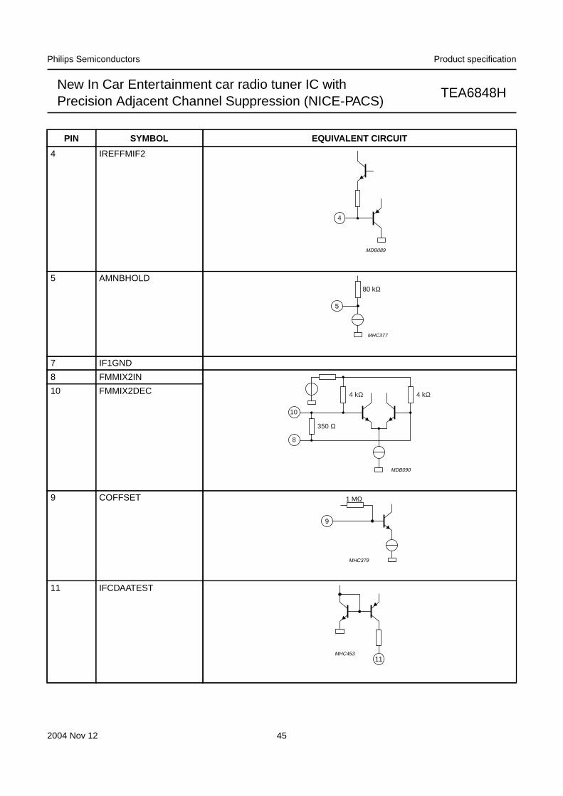
2004 Nov 12 45
Philips Semiconductors Product specification
New In Car Entertainment car radio tuner IC withPrecision Adjacent Channel Suppression (NICE-PACS)
TEA6848H
4 IREFFMIF2
5 AMNBHOLD
7 IF1GND
8 FMMIX2IN
10 FMMIX2DEC
9 COFFSET
11 IFCDAATEST
PIN SYMBOL EQUIVALENT CIRCUIT
MDB089
4
80 kΩ
5
MHC377
MDB090
10
8
350 Ω
4 kΩ 4 kΩ
9
1 MΩ
MHC379
11MHC453

2004 Nov 12 46
Philips Semiconductors Product specification
New In Car Entertainment car radio tuner IC withPrecision Adjacent Channel Suppression (NICE-PACS)
TEA6848H
12 IFAMPOUT
13 VDDA1
14 IFAMPIN
15 IFAMPDEC
16 IF2FILQ
17 IF2FILI
PIN SYMBOL EQUIVALENT CIRCUIT
12330 Ω
MHC381
MDB09114
330 Ω
5kΩ
5kΩ
15
16
MHC455
17 MHC454
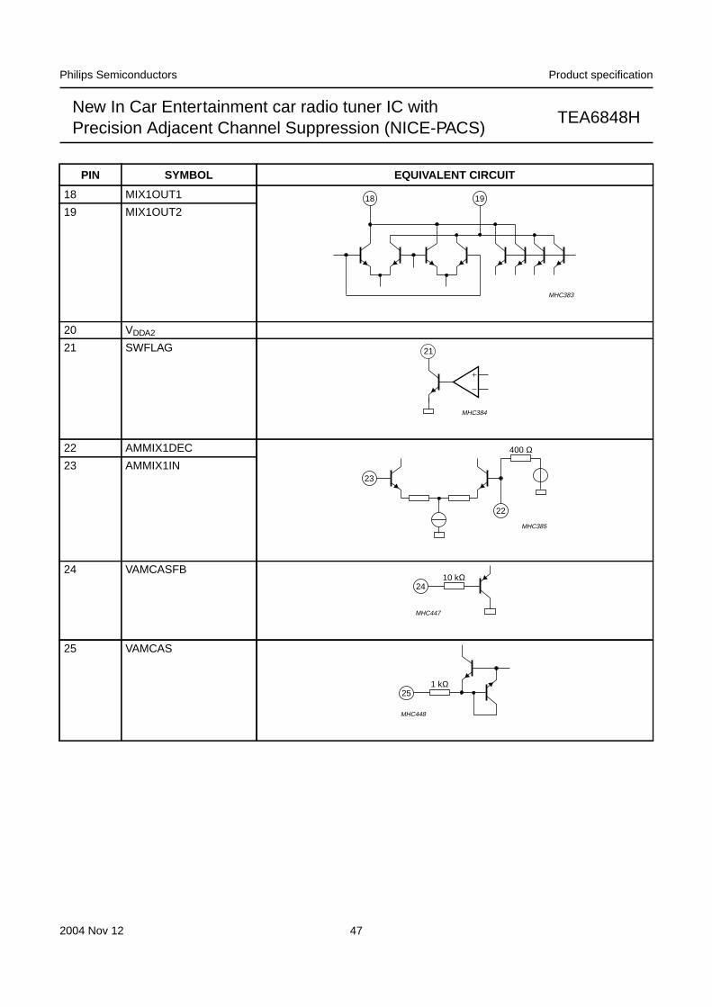
2004 Nov 12 47
Philips Semiconductors Product specification
New In Car Entertainment car radio tuner IC withPrecision Adjacent Channel Suppression (NICE-PACS)
TEA6848H
18 MIX1OUT1
19 MIX1OUT2
20 VDDA2
21 SWFLAG
22 AMMIX1DEC
23 AMMIX1IN
24 VAMCASFB
25 VAMCAS
PIN SYMBOL EQUIVALENT CIRCUIT
1918
MHC383
21
MHC384
23
22
400 Ω
MHC385
2410 kΩ
MHC447
251 kΩ
MHC448
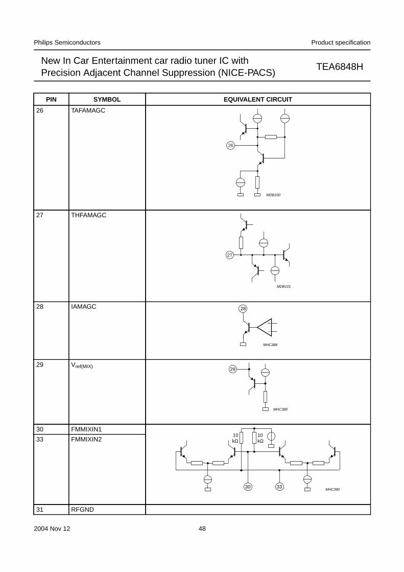
2004 Nov 12 48
Philips Semiconductors Product specification
New In Car Entertainment car radio tuner IC withPrecision Adjacent Channel Suppression (NICE-PACS)
TEA6848H
26 TAFAMAGC
27 THFAMAGC
28 IAMAGC
29 Vref(MIX)
30 FMMIXIN1
33 FMMIXIN2
31 RFGND
PIN SYMBOL EQUIVALENT CIRCUIT
MDB100
26
MDB101
27
28
MHC388
29
MHC389
3330
10kΩ
10kΩ
MHC390
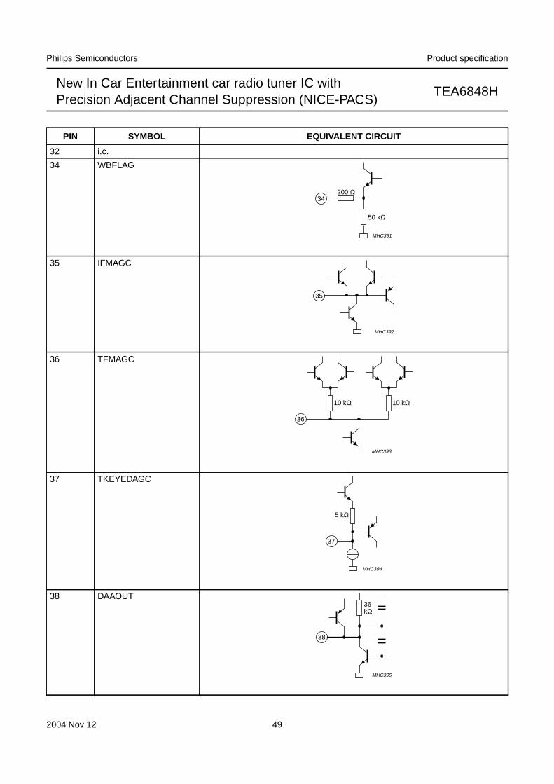
2004 Nov 12 49
Philips Semiconductors Product specification
New In Car Entertainment car radio tuner IC withPrecision Adjacent Channel Suppression (NICE-PACS)
TEA6848H
32 i.c.
34 WBFLAG
35 IFMAGC
36 TFMAGC
37 TKEYEDAGC
38 DAAOUT
PIN SYMBOL EQUIVALENT CIRCUIT
34200 Ω
50 kΩ
MHC391
35
MHC392
10 kΩ
36
10 kΩ
MHC393
5 kΩ
37
MHC394
38
36kΩ
MHC395
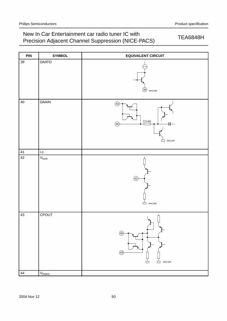
2004 Nov 12 50
Philips Semiconductors Product specification
New In Car Entertainment car radio tuner IC withPrecision Adjacent Channel Suppression (NICE-PACS)
TEA6848H
39 DAATD
40 DAAIN
41 i.c.
42 Vtune
43 CPOUT
44 VDDA3
PIN SYMBOL EQUIVALENT CIRCUIT
39 MHC396
3943
402.5 kΩ
MHC397
42
MHC398
3940
43
MHC399
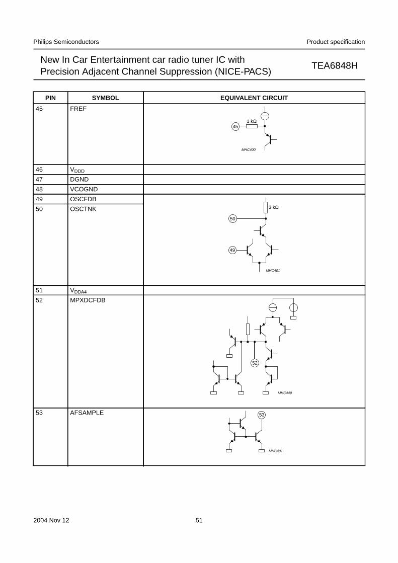
2004 Nov 12 51
Philips Semiconductors Product specification
New In Car Entertainment car radio tuner IC withPrecision Adjacent Channel Suppression (NICE-PACS)
TEA6848H
45 FREF
46 VDDD
47 DGND
48 VCOGND
49 OSCFDB
50 OSCTNK
51 VDDA4
52 MPXDCFDB
53 AFSAMPLE
PIN SYMBOL EQUIVALENT CIRCUIT
451 kΩ
MHC400
49
3 kΩ
50
MHC401
52
MHC449
53
MHC402
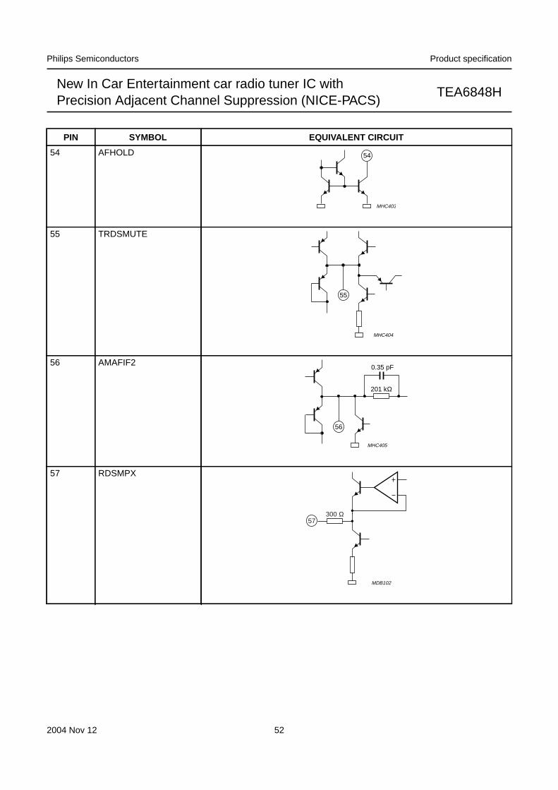
2004 Nov 12 52
Philips Semiconductors Product specification
New In Car Entertainment car radio tuner IC withPrecision Adjacent Channel Suppression (NICE-PACS)
TEA6848H
54 AFHOLD
55 TRDSMUTE
56 AMAFIF2
57 RDSMPX
PIN SYMBOL EQUIVALENT CIRCUIT
54
MHC403
55
MHC404
56
201 kΩ
0.35 pF
MHC405
MDB102
300 Ω57
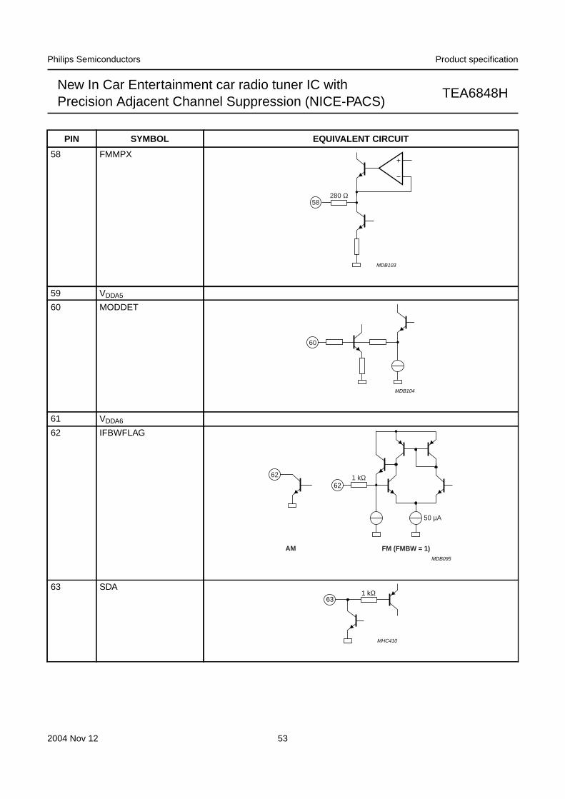
2004 Nov 12 53
Philips Semiconductors Product specification
New In Car Entertainment car radio tuner IC withPrecision Adjacent Channel Suppression (NICE-PACS)
TEA6848H
58 FMMPX
59 VDDA5
60 MODDET
61 VDDA6
62 IFBWFLAG
63 SDA
PIN SYMBOL EQUIVALENT CIRCUIT
MDB103
280 Ω58
MDB104
60
MDB095
1 kΩ
50 µA
62
62
FM (FMBW = 1)AM
631 kΩ
MHC410
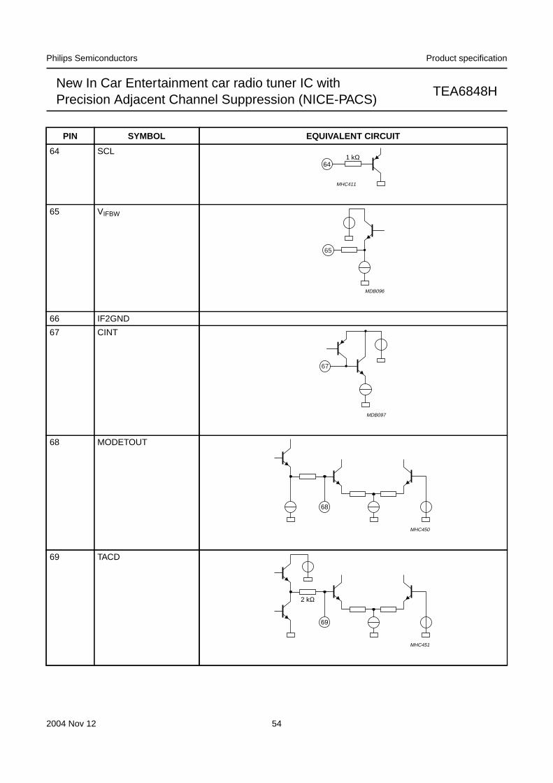
2004 Nov 12 54
Philips Semiconductors Product specification
New In Car Entertainment car radio tuner IC withPrecision Adjacent Channel Suppression (NICE-PACS)
TEA6848H
64 SCL
65 VIFBW
66 IF2GND
67 CINT
68 MODETOUT
69 TACD
PIN SYMBOL EQUIVALENT CIRCUIT
641 kΩ
MHC411
MDB096
65
MDB097
67
68
MHC450
69
2 kΩ
MHC451
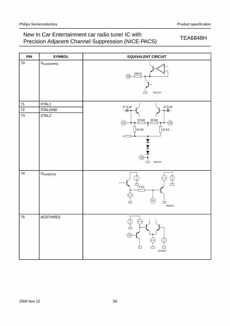
2004 Nov 12 55
Philips Semiconductors Product specification
New In Car Entertainment car radio tuner IC withPrecision Adjacent Channel Suppression (NICE-PACS)
TEA6848H
70 Vlevel(AMFM)
71 XTAL1
72 XTALGND
73 XTAL2
74 Vlevel(ACD)
75 ACDTHRES
PIN SYMBOL EQUIVALENT CIRCUIT
70150 Ω
MHC414
73
72
71
27.6 pF
10 kΩ
20 kΩ
27.6 pF
20 kΩ
10 kΩ
MHC415
MDB212
74
8 kΩ
MDB099
75
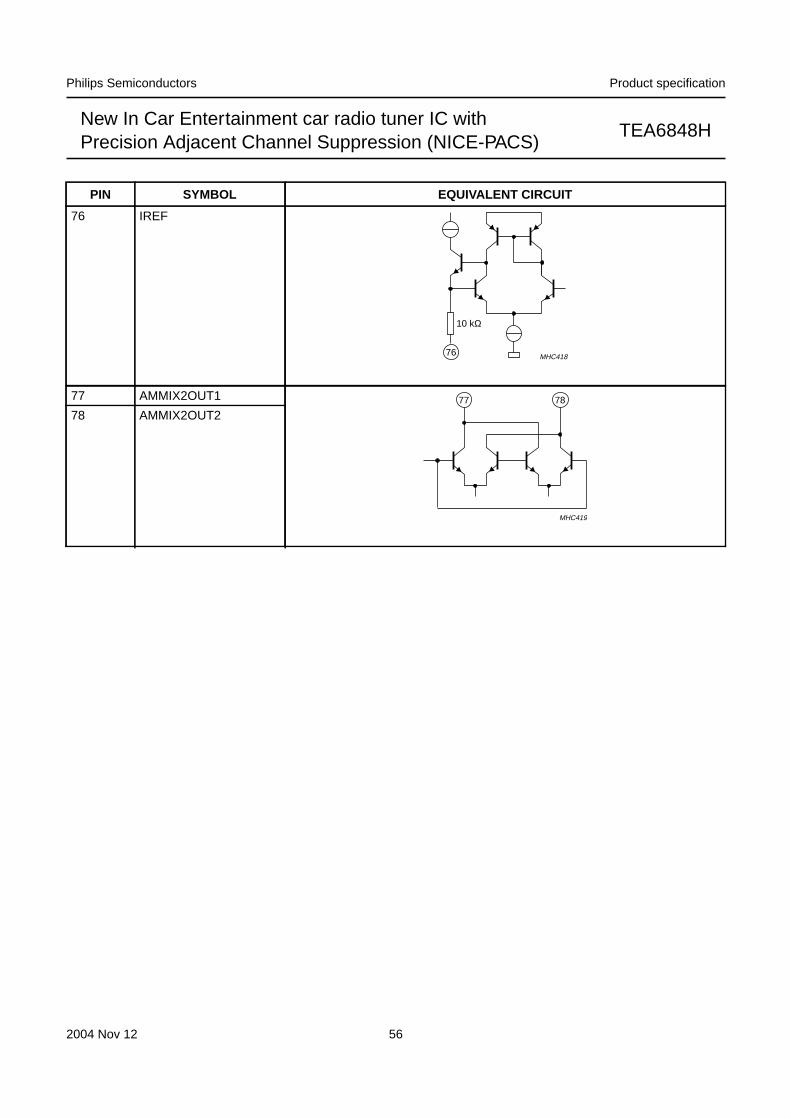
2004 Nov 12 56
Philips Semiconductors Product specification
New In Car Entertainment car radio tuner IC withPrecision Adjacent Channel Suppression (NICE-PACS)
TEA6848H
76 IREF
77 AMMIX2OUT1
78 AMMIX2OUT2
PIN SYMBOL EQUIVALENT CIRCUIT
76
10 kΩ
MHC418
7877
MHC419

2004 Nov 12 57
Philips Semiconductors Product specification
New In Car Entertainment car radio tuner IC withPrecision Adjacent Channel Suppression (NICE-PACS)
TEA6848H
79 CAGC
80 Vref(lim)
PIN SYMBOL EQUIVALENT CIRCUIT
MDB092
79
AM
79
420 Ω
10 kΩ
FM
80
MHC452
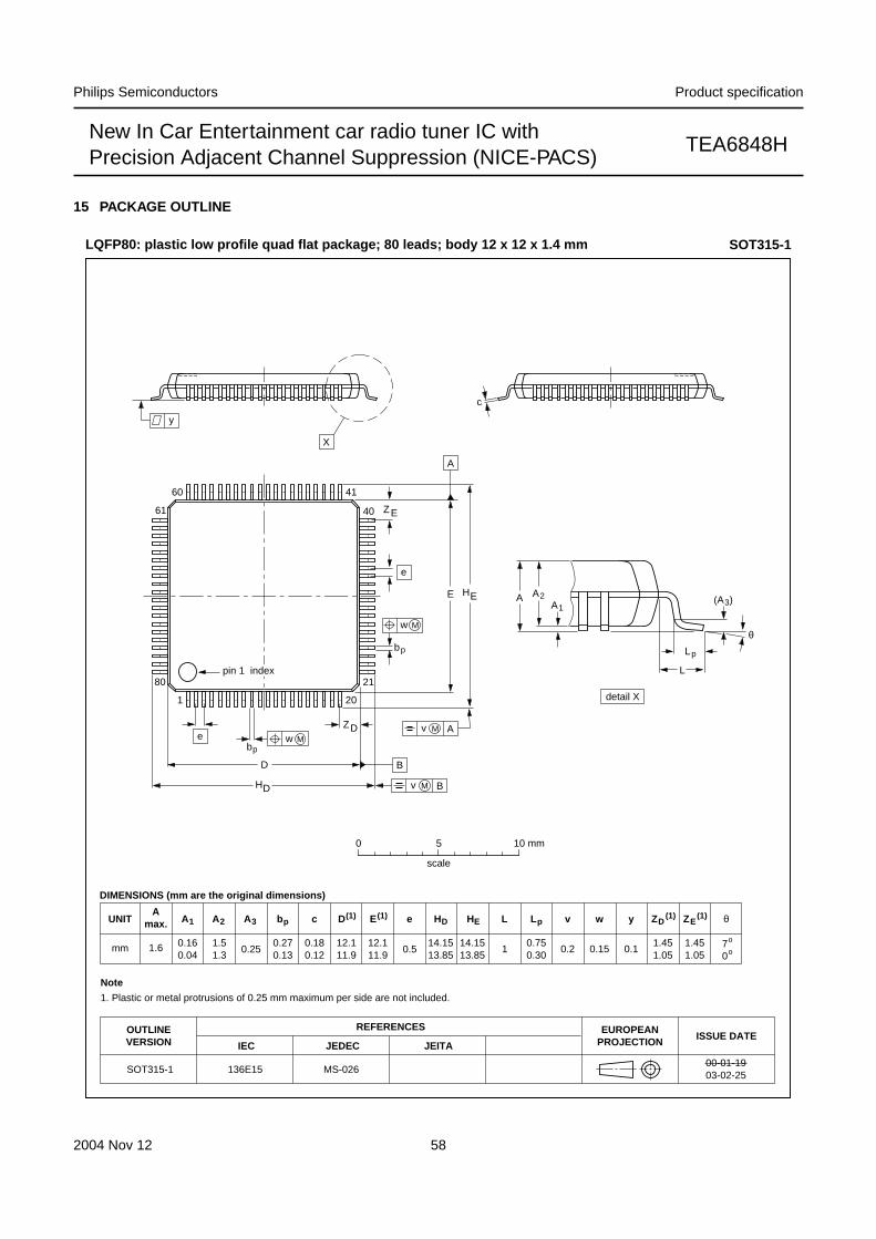
2004 Nov 12 58
Philips Semiconductors Product specification
New In Car Entertainment car radio tuner IC withPrecision Adjacent Channel Suppression (NICE-PACS)
TEA6848H
15 PACKAGE OUTLINE
UNITA
max. A1 A2 A3 bp c E(1) e HE L L p Zywv θ
REFERENCESOUTLINEVERSION
EUROPEANPROJECTION ISSUE DATE
IEC JEDEC JEITA
mm 1.6 0.160.04
1.51.3
0.250.270.13
0.180.12
12.111.9
0.514.1513.85
1.451.05
70
o
o0.15 0.10.21
DIMENSIONS (mm are the original dimensions)
Note
1. Plastic or metal protrusions of 0.25 mm maximum per side are not included.
0.750.30
SOT315-1 136E15 MS-02600-01-1903-02-25
D(1) (1)(1)
12.111.9
HD
14.1513.85
EZ
1.451.05
D
bp
e
θ
EA1
A
Lp
detail X
L
(A )3
B
20
c
DH
bp
EH A2
v M B
D
ZD
A
ZE
e
v M A
X
1
80
61
60 41
40
21
y
pin 1 index
w M
w M
0 5 10 mm
scale
LQFP80: plastic low profile quad flat package; 80 leads; body 12 x 12 x 1.4 mm SOT315-1
2004 Nov 12 59
Philips Semiconductors Product specification
New In Car Entertainment car radio tuner IC withPrecision Adjacent Channel Suppression (NICE-PACS)
TEA6848H
16 SOLDERING
16.1 Introduction to soldering surface mountpackages
This text gives a very brief insight to a complex technology.A more in-depth account of soldering ICs can be found inour “Data Handbook IC26; Integrated Circuit Packages”(document order number 9398 652 90011).
There is no soldering method that is ideal for all surfacemount IC packages. Wave soldering can still be used forcertain surface mount ICs, but it is not suitable for fine pitchSMDs. In these situations reflow soldering isrecommended.
16.2 Reflow soldering
Reflow soldering requires solder paste (a suspension offine solder particles, flux and binding agent) to be appliedto the printed-circuit board by screen printing, stencilling orpressure-syringe dispensing before package placement.Driven by legislation and environmental forces theworldwide use of lead-free solder pastes is increasing.
Several methods exist for reflowing; for example,convection or convection/infrared heating in a conveyortype oven. Throughput times (preheating, soldering andcooling) vary between 100 seconds and 200 secondsdepending on heating method.
Typical reflow peak temperatures range from215 °C to 270 °C depending on solder paste material. Thetop-surface temperature of the packages shouldpreferably be kept:
• below 225 °C (SnPb process) or below 245 °C (Pb-freeprocess)
– for all BGA, HTSSON..T and SSOP..T packages
– for packages with a thickness ≥ 2.5 mm
– for packages with a thickness < 2.5 mm and avolume ≥ 350 mm3 so called thick/large packages.
• below 240 °C (SnPb process) or below 260 °C (Pb-freeprocess) for packages with a thickness < 2.5 mm and avolume < 350 mm3 so called small/thin packages.
Moisture sensitivity precautions, as indicated on packing,must be respected at all times.
16.3 Wave soldering
Conventional single wave soldering is not recommendedfor surface mount devices (SMDs) or printed-circuit boardswith a high component density, as solder bridging andnon-wetting can present major problems.
To overcome these problems the double-wave solderingmethod was specifically developed.
If wave soldering is used the following conditions must beobserved for optimal results:
• Use a double-wave soldering method comprising aturbulent wave with high upward pressure followed by asmooth laminar wave.
• For packages with leads on two sides and a pitch (e):
– larger than or equal to 1.27 mm, the footprintlongitudinal axis is preferred to be parallel to thetransport direction of the printed-circuit board;
– smaller than 1.27 mm, the footprint longitudinal axismust be parallel to the transport direction of theprinted-circuit board.
The footprint must incorporate solder thieves at thedownstream end.
• For packages with leads on four sides, the footprint mustbe placed at a 45° angle to the transport direction of theprinted-circuit board. The footprint must incorporatesolder thieves downstream and at the side corners.
During placement and before soldering, the package mustbe fixed with a droplet of adhesive. The adhesive can beapplied by screen printing, pin transfer or syringedispensing. The package can be soldered after theadhesive is cured.
Typical dwell time of the leads in the wave ranges from3 seconds to 4 seconds at 250 °C or 265 °C, dependingon solder material applied, SnPb or Pb-free respectively.
A mildly-activated flux will eliminate the need for removalof corrosive residues in most applications.
16.4 Manual soldering
Fix the component by first soldering twodiagonally-opposite end leads. Use a low voltage (24 V orless) soldering iron applied to the flat part of the lead.Contact time must be limited to 10 seconds at up to300 °C.
When using a dedicated tool, all other leads can besoldered in one operation within 2 seconds to 5 secondsbetween 270 °C and 320 °C.
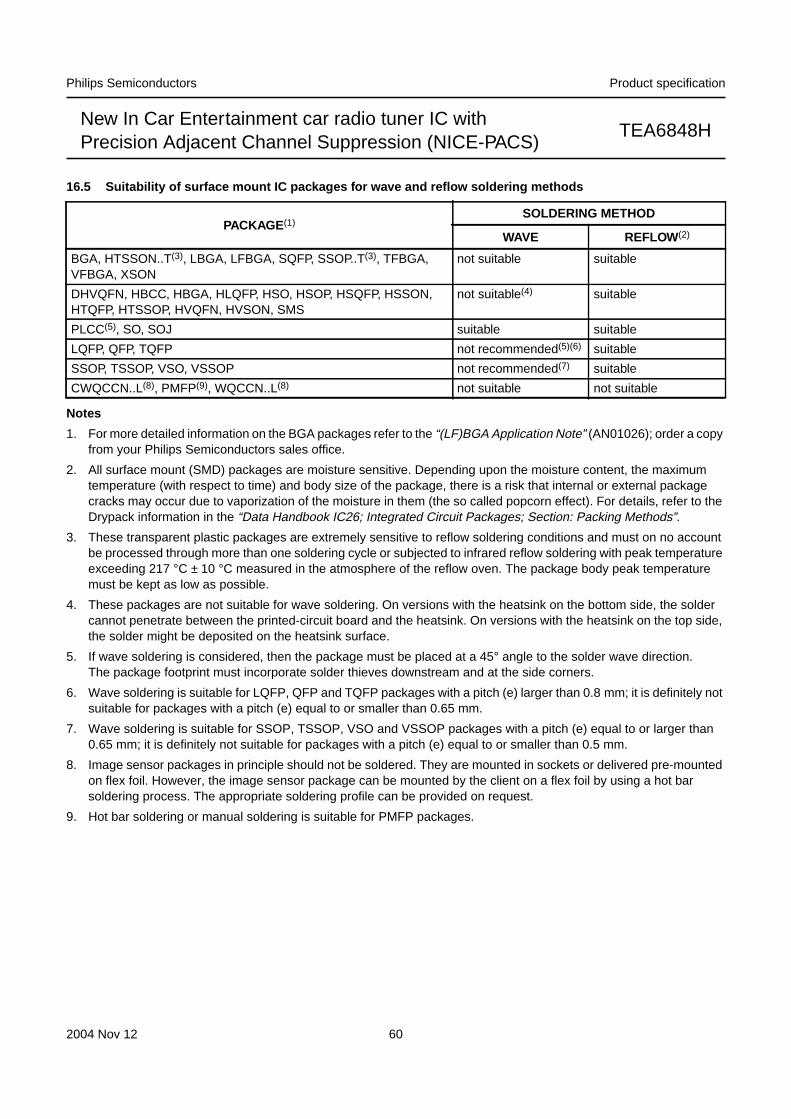
2004 Nov 12 60
Philips Semiconductors Product specification
New In Car Entertainment car radio tuner IC withPrecision Adjacent Channel Suppression (NICE-PACS)
TEA6848H
16.5 Suitability of surface mount IC packages for wave and reflow soldering methods
Notes
1. For more detailed information on the BGA packages refer to the “(LF)BGA Application Note” (AN01026); order a copyfrom your Philips Semiconductors sales office.
2. All surface mount (SMD) packages are moisture sensitive. Depending upon the moisture content, the maximumtemperature (with respect to time) and body size of the package, there is a risk that internal or external packagecracks may occur due to vaporization of the moisture in them (the so called popcorn effect). For details, refer to theDrypack information in the “Data Handbook IC26; Integrated Circuit Packages; Section: Packing Methods”.
3. These transparent plastic packages are extremely sensitive to reflow soldering conditions and must on no accountbe processed through more than one soldering cycle or subjected to infrared reflow soldering with peak temperatureexceeding 217 °C ± 10 °C measured in the atmosphere of the reflow oven. The package body peak temperaturemust be kept as low as possible.
4. These packages are not suitable for wave soldering. On versions with the heatsink on the bottom side, the soldercannot penetrate between the printed-circuit board and the heatsink. On versions with the heatsink on the top side,the solder might be deposited on the heatsink surface.
5. If wave soldering is considered, then the package must be placed at a 45° angle to the solder wave direction.The package footprint must incorporate solder thieves downstream and at the side corners.
6. Wave soldering is suitable for LQFP, QFP and TQFP packages with a pitch (e) larger than 0.8 mm; it is definitely notsuitable for packages with a pitch (e) equal to or smaller than 0.65 mm.
7. Wave soldering is suitable for SSOP, TSSOP, VSO and VSSOP packages with a pitch (e) equal to or larger than0.65 mm; it is definitely not suitable for packages with a pitch (e) equal to or smaller than 0.5 mm.
8. Image sensor packages in principle should not be soldered. They are mounted in sockets or delivered pre-mountedon flex foil. However, the image sensor package can be mounted by the client on a flex foil by using a hot barsoldering process. The appropriate soldering profile can be provided on request.
9. Hot bar soldering or manual soldering is suitable for PMFP packages.
PACKAGE (1)SOLDERING METHOD
WAVE REFLOW (2)
BGA, HTSSON..T(3), LBGA, LFBGA, SQFP, SSOP..T(3), TFBGA,VFBGA, XSON
not suitable suitable
DHVQFN, HBCC, HBGA, HLQFP, HSO, HSOP, HSQFP, HSSON,HTQFP, HTSSOP, HVQFN, HVSON, SMS
not suitable(4) suitable
PLCC(5), SO, SOJ suitable suitable
LQFP, QFP, TQFP not recommended(5)(6) suitable
SSOP, TSSOP, VSO, VSSOP not recommended(7) suitable
CWQCCN..L(8), PMFP(9), WQCCN..L(8) not suitable not suitable
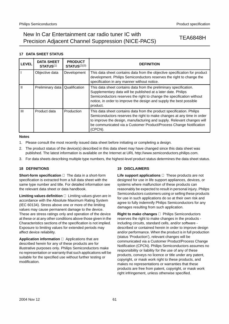
2004 Nov 12 61
Philips Semiconductors Product specification
New In Car Entertainment car radio tuner IC withPrecision Adjacent Channel Suppression (NICE-PACS)
TEA6848H
17 DATA SHEET STATUS
Notes
1. Please consult the most recently issued data sheet before initiating or completing a design.
2. The product status of the device(s) described in this data sheet may have changed since this data sheet waspublished. The latest information is available on the Internet at URL http://www.semiconductors.philips.com.
3. For data sheets describing multiple type numbers, the highest-level product status determines the data sheet status.
LEVELDATA SHEET
STATUS(1)PRODUCT
STATUS(2)(3) DEFINITION
I Objective data Development This data sheet contains data from the objective specification for productdevelopment. Philips Semiconductors reserves the right to change thespecification in any manner without notice.
II Preliminary data Qualification This data sheet contains data from the preliminary specification.Supplementary data will be published at a later date. PhilipsSemiconductors reserves the right to change the specification withoutnotice, in order to improve the design and supply the best possibleproduct.
III Product data Production This data sheet contains data from the product specification. PhilipsSemiconductors reserves the right to make changes at any time in orderto improve the design, manufacturing and supply. Relevant changes willbe communicated via a Customer Product/Process Change Notification(CPCN).
18 DEFINITIONS
Short-form specification The data in a short-formspecification is extracted from a full data sheet with thesame type number and title. For detailed information seethe relevant data sheet or data handbook.
Limiting values definition Limiting values given are inaccordance with the Absolute Maximum Rating System(IEC 60134). Stress above one or more of the limitingvalues may cause permanent damage to the device.These are stress ratings only and operation of the deviceat these or at any other conditions above those given in theCharacteristics sections of the specification is not implied.Exposure to limiting values for extended periods mayaffect device reliability.
Application information Applications that aredescribed herein for any of these products are forillustrative purposes only. Philips Semiconductors makeno representation or warranty that such applications will besuitable for the specified use without further testing ormodification.
19 DISCLAIMERS
Life support applications These products are notdesigned for use in life support appliances, devices, orsystems where malfunction of these products canreasonably be expected to result in personal injury. PhilipsSemiconductors customers using or selling these productsfor use in such applications do so at their own risk andagree to fully indemnify Philips Semiconductors for anydamages resulting from such application.
Right to make changes Philips Semiconductorsreserves the right to make changes in the products -including circuits, standard cells, and/or software -described or contained herein in order to improve designand/or performance. When the product is in full production(status ‘Production’), relevant changes will becommunicated via a Customer Product/Process ChangeNotification (CPCN). Philips Semiconductors assumes noresponsibility or liability for the use of any of theseproducts, conveys no licence or title under any patent,copyright, or mask work right to these products, andmakes no representations or warranties that theseproducts are free from patent, copyright, or mask workright infringement, unless otherwise specified.
2004 Nov 12 62
Philips Semiconductors Product specification
New In Car Entertainment car radio tuner IC withPrecision Adjacent Channel Suppression (NICE-PACS)
TEA6848H
20 PURCHASE OF PHILIPS I2C COMPONENTS
Purchase of Philips I2C components conveys a license under the Philips’ I2C patent to use thecomponents in the I2C system provided the system conforms to the I2C specification defined byPhilips. This specification can be ordered using the code 9398 393 40011.

© Koninklijke Philips Electronics N.V. 2004 SCA76All rights are reserved. Reproduction in whole or in part is prohibited without the prior written consent of the copyright owner.
The information presented in this document does not form part of any quotation or contract, is believed to be accurate and reliable and may be changedwithout notice. No liability will be accepted by the publisher for any consequence of its use. Publication thereof does not convey nor imply any licenseunder patent- or other industrial or intellectual property rights.
Philips Semiconductors – a worldwide company
Contact information
For additional information please visit http://www.semiconductors.philips.com . Fax: +31 40 27 24825For sales offices addresses send e-mail to: [email protected] .
Printed in The Netherlands R32/03/pp63 Date of release: 2004 Nov 12 Document order number: 9397 750 14272