Embed Size (px)
Citation preview
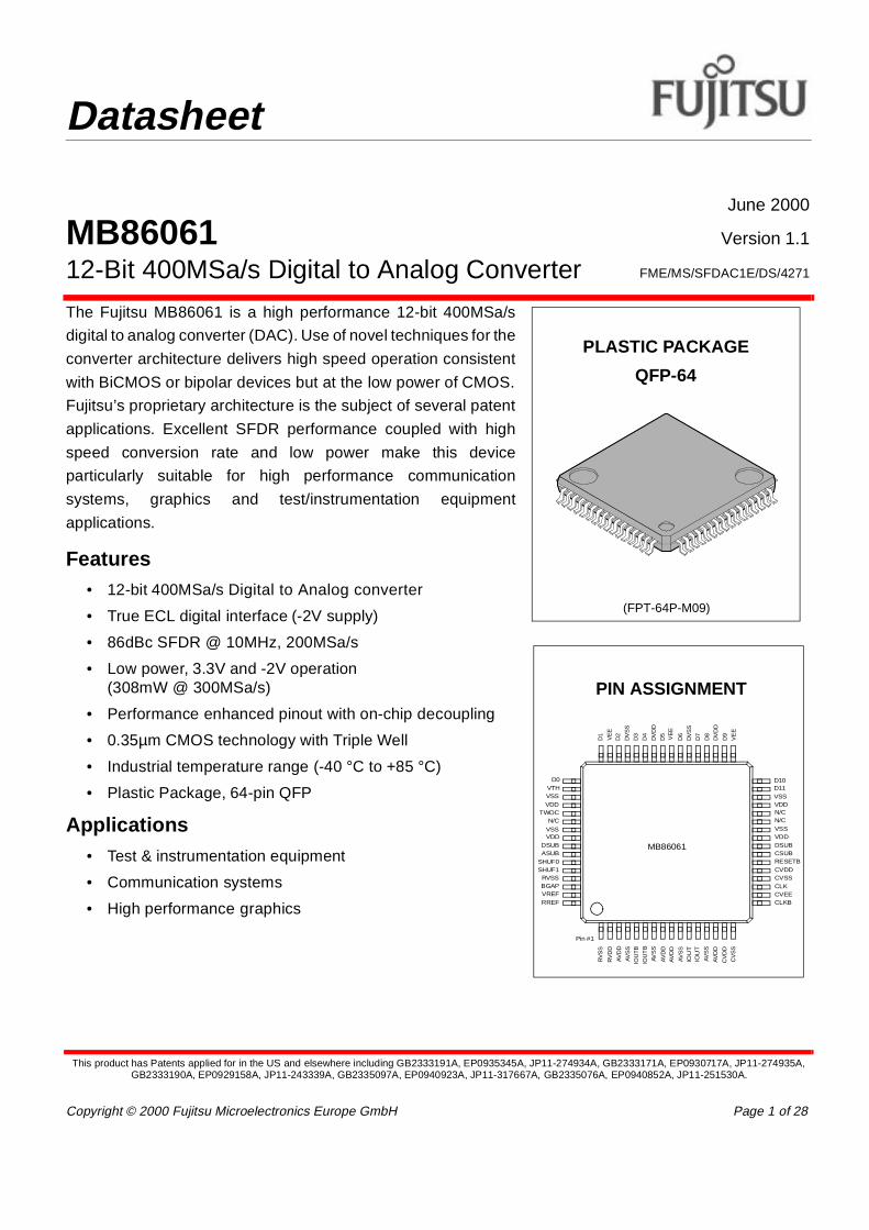
Datasheet
June 2000
MB86061 Version 1.1
12-Bit 400MSa/s Digital to Analog Converter FME/MS/SFDAC1E/DS/4271
This product has Patents applied for in the US and elsewhere including GB2333191A, EP0935345A, JP11-274934A, GB2333171A, EP0930717A, JP11-274935A, GB2333190A, EP0929158A, JP11-243339A, GB2335097A, EP0940923A, JP11-317667A, GB2335076A, EP0940852A, JP11-251530A.
Copyright © 2000 Fujitsu Microelectronics Europe GmbH Page 1 of 28
The Fujitsu MB86061 is a high performance 12-bit 400MSa/s
digital to analog converter (DAC). Use of novel techniques for the
converter architecture delivers high speed operation consistent
with BiCMOS or bipolar devices but at the low power of CMOS.
Fujitsu’s proprietary architecture is the subject of several patent
applications. Excellent SFDR performance coupled with high
speed conversion rate and low power make this device
particularly suitable for high performance communication
systems, graphics and test/instrumentation equipment
applications.
Features• 12-bit 400MSa/s Digital to Analog converter
• True ECL digital interface (-2V supply)
• 86dBc SFDR @ 10MHz, 200MSa/s
• Low power, 3.3V and -2V operation(308mW @ 300MSa/s)
• Performance enhanced pinout with on-chip decoupling
• 0.35µm CMOS technology with Triple Well
• Industrial temperature range (-40 °C to +85 °C)
• Plastic Package, 64-pin QFP
Applications• Test & instrumentation equipment
• Communication systems
• High performance graphics
(FPT-64P-M09)
PLASTIC PACKAGE
QFP-64
PIN ASSIGNMENT
N/CN/CVSSVDDDSUBCSUBRESETBCVDDCVSSCLKCVEECLKB
RV
SS
RV
DD
AV
DD
AV
SS
IOU
TB
IOU
TB
AV
DD
AVS
S
AV
DD
AV
SS
AV
DD
CV
DD
CV
SS
D2
DV
SS
D3
D4
DV
DD
D5
D6
DV
SS
D7
D8
DV
DD
D9
VE
E
VDD
D11VSS
D10
VSSVDD
TWOCN/C
VDDVSS
DSUBASUB
SHUF1SHUF0
RVSSBGAPVREFRREF
Pin #1
D1
VE
E
MB86061
D0VTH
IOU
TIO
UT
AV
SS
VE
E

June 2000 Version 1.1FME/MS/SFDAC1E/DS/4271
MB86061 12-Bit 400MSa/s Digital to Analog Converter
Page 2 of 28 Copyright © 2000 Fujitsu Microelectronics Europe GmbH
Contents
1 Functional Description . . . . . . . . . . . . . . . . . . . . . . . . . . . . . . . . . . . . . .31.1 Operating Modes . . . . . . . . . . . . . . . . . . . . . . . . . . . . . . . . . . . . . . . .3
1.1.1 Segment Shuffling . . . . . . . . . . . . . . . . . . . . . . . . . . . . . . . . .41.2 Voltage Reference . . . . . . . . . . . . . . . . . . . . . . . . . . . . . . . . . . . . . . .41.3 Analog Output . . . . . . . . . . . . . . . . . . . . . . . . . . . . . . . . . . . . . . . . . .4
1.3.1 Analog Output Reference Resistor . . . . . . . . . . . . . . . . . . . .51.3.2 Analog Output Scaling . . . . . . . . . . . . . . . . . . . . . . . . . . . . .51.3.3 Analog Output Pins . . . . . . . . . . . . . . . . . . . . . . . . . . . . . . . .5
1.4 Digital Data Interface . . . . . . . . . . . . . . . . . . . . . . . . . . . . . . . . . . . . .51.5 Power Supplies . . . . . . . . . . . . . . . . . . . . . . . . . . . . . . . . . . . . . . . . .6
1.5.1 Substrate Connections . . . . . . . . . . . . . . . . . . . . . . . . . . . . .61.5.2 Power Dissipation . . . . . . . . . . . . . . . . . . . . . . . . . . . . . . . . .61.5.3 Pinout . . . . . . . . . . . . . . . . . . . . . . . . . . . . . . . . . . . . . . . . . .6
1.6 Reset . . . . . . . . . . . . . . . . . . . . . . . . . . . . . . . . . . . . . . . . . . . . . . . . .7
2 Timing Diagrams . . . . . . . . . . . . . . . . . . . . . . . . . . . . . . . . . . . . . . . . . . .8
3 Electrical Specifications . . . . . . . . . . . . . . . . . . . . . . . . . . . . . . . . . . . . .93.1 Absolute Maximum Ratings . . . . . . . . . . . . . . . . . . . . . . . . . . . . . . . .93.2 Digital Interface Specifications . . . . . . . . . . . . . . . . . . . . . . . . . . . . .103.3 DC Specifications . . . . . . . . . . . . . . . . . . . . . . . . . . . . . . . . . . . . . . .113.4 AC Specifications . . . . . . . . . . . . . . . . . . . . . . . . . . . . . . . . . . . . . . .123.5 Clock Specifications . . . . . . . . . . . . . . . . . . . . . . . . . . . . . . . . . . . . .133.6 Typical Performance Characterisation Graphs . . . . . . . . . . . . . . . .14
4 Application Notes . . . . . . . . . . . . . . . . . . . . . . . . . . . . . . . . . . . . . . . . . .154.1 Power & Ground Plane Regions . . . . . . . . . . . . . . . . . . . . . . . . . . .154.2 Power Supplies . . . . . . . . . . . . . . . . . . . . . . . . . . . . . . . . . . . . . . . .174.3 Decoupling . . . . . . . . . . . . . . . . . . . . . . . . . . . . . . . . . . . . . . . . . . . .184.4 Analog Output . . . . . . . . . . . . . . . . . . . . . . . . . . . . . . . . . . . . . . . . .194.5 Clock Input . . . . . . . . . . . . . . . . . . . . . . . . . . . . . . . . . . . . . . . . . . . .19
5 Pin Description . . . . . . . . . . . . . . . . . . . . . . . . . . . . . . . . . . . . . . . . . . . .215.1 Pin Assignment . . . . . . . . . . . . . . . . . . . . . . . . . . . . . . . . . . . . . . . .215.2 Pin Definition . . . . . . . . . . . . . . . . . . . . . . . . . . . . . . . . . . . . . . . . . .225.3 Package Data . . . . . . . . . . . . . . . . . . . . . . . . . . . . . . . . . . . . . . . . .24
5.3.1 Thermal Characteristics . . . . . . . . . . . . . . . . . . . . . . . . . . .245.4 Ordering Information . . . . . . . . . . . . . . . . . . . . . . . . . . . . . . . . . . . .24
6 Development Kit . . . . . . . . . . . . . . . . . . . . . . . . . . . . . . . . . . . . . . . . . . .25
June 2000 Version 1.1FME/MS/SFDAC1E/DS/4271
MB86061 12-Bit 400MSa/s Digital to Analog Converter
Copyright © 2000 Fujitsu Microelectronics Europe GmbH Page 3 of 28
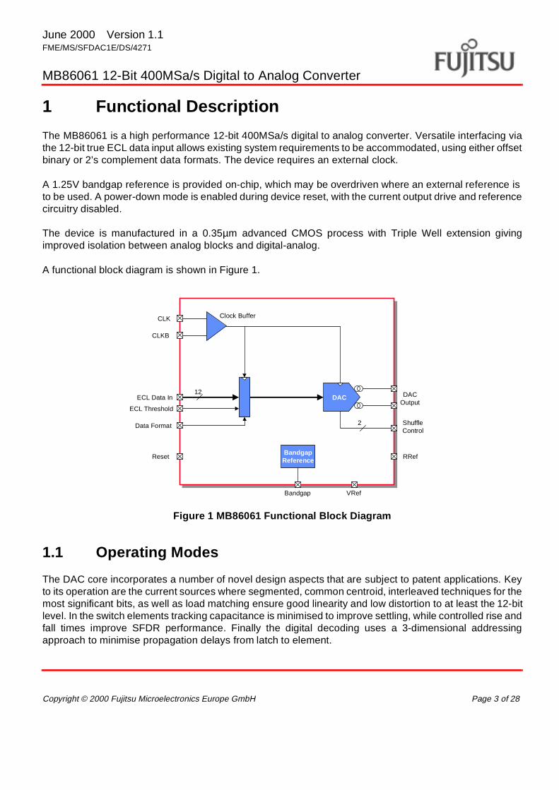
1 Functional Description
The MB86061 is a high performance 12-bit 400MSa/s digital to analog converter. Versatile interfacing viathe 12-bit true ECL data input allows existing system requirements to be accommodated, using either offsetbinary or 2’s complement data formats. The device requires an external clock.
A 1.25V bandgap reference is provided on-chip, which may be overdriven where an external reference isto be used. A power-down mode is enabled during device reset, with the current output drive and referencecircuitry disabled.
The device is manufactured in a 0.35µm advanced CMOS process with Triple Well extension givingimproved isolation between analog blocks and digital-analog.
A functional block diagram is shown in Figure 1.
Figure 1 MB86061 Functional Block Diagram
1.1 Operating Modes
The DAC core incorporates a number of novel design aspects that are subject to patent applications. Keyto its operation are the current sources where segmented, common centroid, interleaved techniques for themost significant bits, as well as load matching ensure good linearity and low distortion to at least the 12-bitlevel. In the switch elements tracking capacitance is minimised to improve settling, while controlled rise andfall times improve SFDR performance. Finally the digital decoding uses a 3-dimensional addressingapproach to minimise propagation delays from latch to element.
FML Mixed Signal
DAC12
ECL Data In
CLK
DACOutput
ResetBandgapReference
Data Format
CLKB
Bandgap
Clock Buffer
ECL Threshold
ShuffleControl
2
RRef
VRef
June 2000 Version 1.1FME/MS/SFDAC1E/DS/4271
MB86061 12-Bit 400MSa/s Digital to Analog Converter
Page 4 of 28 Copyright © 2000 Fujitsu Microelectronics Europe GmbH
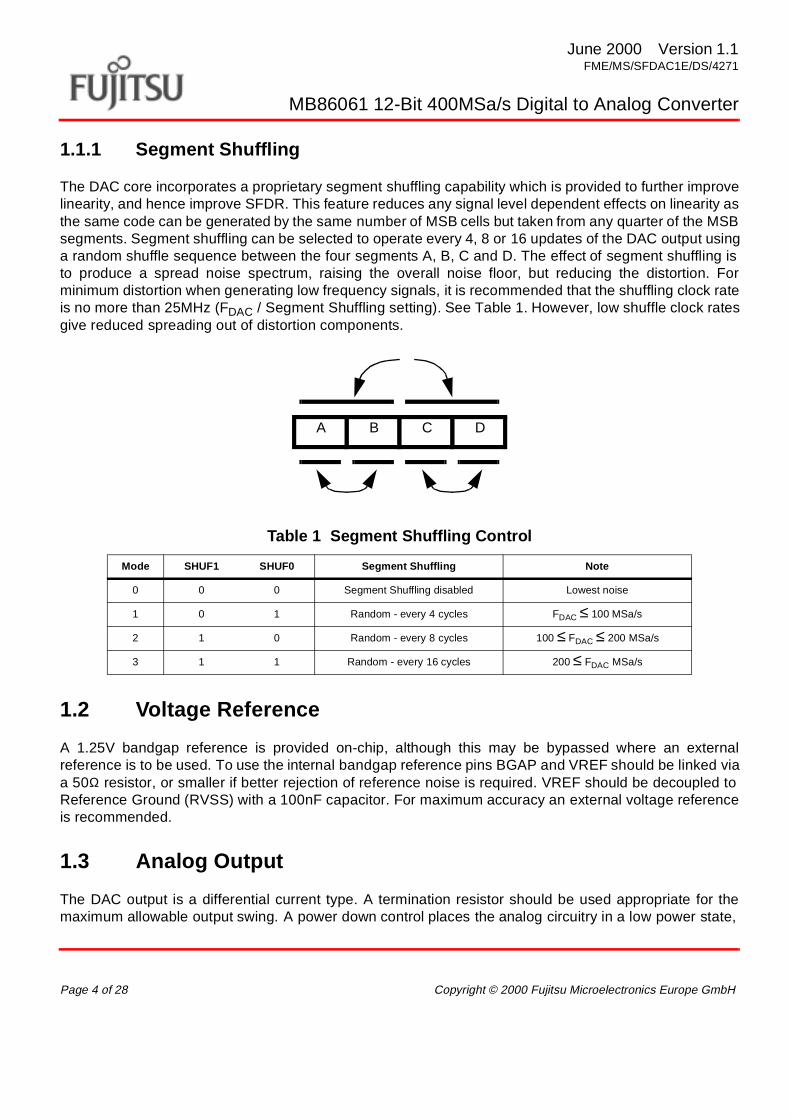
1.1.1 Segment Shuffling
The DAC core incorporates a proprietary segment shuffling capability which is provided to further improvelinearity, and hence improve SFDR. This feature reduces any signal level dependent effects on linearity asthe same code can be generated by the same number of MSB cells but taken from any quarter of the MSBsegments. Segment shuffling can be selected to operate every 4, 8 or 16 updates of the DAC output usinga random shuffle sequence between the four segments A, B, C and D. The effect of segment shuffling isto produce a spread noise spectrum, raising the overall noise floor, but reducing the distortion. Forminimum distortion when generating low frequency signals, it is recommended that the shuffling clock rateis no more than 25MHz (FDAC / Segment Shuffling setting). See Table 1. However, low shuffle clock ratesgive reduced spreading out of distortion components.
1.2 Voltage Reference
A 1.25V bandgap reference is provided on-chip, although this may be bypassed where an externalreference is to be used. To use the internal bandgap reference pins BGAP and VREF should be linked viaa 50Ω resistor, or smaller if better rejection of reference noise is required. VREF should be decoupled toReference Ground (RVSS) with a 100nF capacitor. For maximum accuracy an external voltage referenceis recommended.
1.3 Analog Output
The DAC output is a differential current type. A termination resistor should be used appropriate for themaximum allowable output swing. A power down control places the analog circuitry in a low power state,
Table 1 Segment Shuffling Control
Mode SHUF1 SHUF0 Segment Shuffling Note
0 0 0 Segment Shuffling disabled Lowest noise
1 0 1 Random - every 4 cycles FDAC ≤ 100 MSa/s
2 1 0 Random - every 8 cycles 100 ≤ FDAC ≤ 200 MSa/s
3 1 1 Random - every 16 cycles 200 ≤ FDAC MSa/s
A B C D
June 2000 Version 1.1FME/MS/SFDAC1E/DS/4271
MB86061 12-Bit 400MSa/s Digital to Analog Converter
Copyright © 2000 Fujitsu Microelectronics Europe GmbH Page 5 of 28
switching off the current output drive and reference circuitry. When power down mode is selected thedevice enters its reset state setting the input data code to +1/2 in 2’s complement, or 0 in unsigned binary.
1.3.1 Analog Output Reference Resistor
From the voltage reference a control loop defines the current through an external resistor, Rref, where thecurrent in the reference resistor is 4 times the internal segment current, and the full scale output current isdefined as,
therefore,
e.g. Using a 1.25V Vref., to give a 20mA full scale output => RRef = 1kΩ
1.3.2 Analog Output Scaling
Power savings can be made by reducing the full scale analog output current (IOP) by increasing Rref.However, to maintain the specified performance, IOP should be programmed to 20mA, and the digital datashould be pre-scaled to achieve full scale deflection at an output current lower than full scale (IOP).
1.3.3 Analog Output Pins
The analog outputs, IOUT and IOUTB, are each connected to two pins to reduce output inductance. Thesepins should be directly connected together on the PCB.
1.4 Digital Data Interface
12-bit digital data is input through pins D[11:0]. D11 is the MSB. Data may be presented in either UnsignedBinary or 2’s Complement format, depending upon the setting of the TWOC pin. See Table 3.
Table 2 Full Scale Code Representation
2’s Complement Unsigned Binary
Code IOUT IOUTB Code IOUT IOUTB
+2047 0111 1111 1111 65/64.IFS1/64.IFS 4095 1111 1111 1111 65/64.IFS
1/64.IFS
: : : : : : : :
0 0000 0000 0000 33/64.IFS33/64.IFS 2048 1000 0000 0000 33/64.IFS
33/64.IFS
: : : : : : : :
-2048 1000 0000 0000 1/64.IFS65/64.IFS 0 0000 0000 0000 1/64.IFS
65/64.IFS
IOP 636364------
Vref4 Rref×--------------------
× 16 I ref⋅≈=
Rref
16 Vref×IOP
---------------------=
June 2000 Version 1.1FME/MS/SFDAC1E/DS/4271
MB86061 12-Bit 400MSa/s Digital to Analog Converter
Page 6 of 28 Copyright © 2000 Fujitsu Microelectronics Europe GmbH
Note: The Digital Data interface has true ECL inputs. The voltage levels of the input data must not exceedthe specifications in section 3.2.
1.5 Power Supplies
Separate power and ground supplies are used for the digital data, digital control, analog, reference andclock circuits. A low jitter supply, free from data dependent signals is required by the clock domain. A supplywith low clock and data noise is required for the analog domain. The clock, digital control, analog andreference circuitry are all implemented using Fujitsu’s Triple-Well extension to the standard CMOS processto provide the necessary electrical isolation. Individual substrate connections are provided to analog, digitalcontrol and clock domains.
1.5.1 Substrate Connections
Connections to the analog, digital control, and clock block substrates are provided. These pins wouldtypically be directly connected to the main digital ground (VSS), so as to direct any noise that has beencollected by the substrates away from the analog blocks.
1.5.2 Power Dissipation
The power dissipation, PD, is dependant on specific operating conditions: supply voltage (VDD), full scaleoutput current (IOP), DAC output update rate (FDAC) and input data waveform. Equations for calculatingpower dissipation are given in section 3.3.
Depending on these factors, applications requiring high FDAC frequencies and/or extended lifetime atambient temperatures >70oC may need additional cooling.
1.5.3 Pinout
The MB86061 features a performance enhanced pinout to gain the maximum performance from the PCB.Ground connection pins are provided adjacent to clock in and analog out pins to minimise the loopinductance of the return current path. All critical power supplies are paired on adjacent pins to minimise thedecoupling loop inductance, and small value decoupling is provided on-chip. Discrete decoupling, typically100nF, must be provided for each power supply pin pair. See section 4.
Table 3 Digital Data Format Control Pin Function
TWOC Digital Data Format
0 Unsigned Binary
1 2’s Complement
June 2000 Version 1.1FME/MS/SFDAC1E/DS/4271
MB86061 12-Bit 400MSa/s Digital to Analog Converter
Copyright © 2000 Fujitsu Microelectronics Europe GmbH Page 7 of 28
1.6 Reset
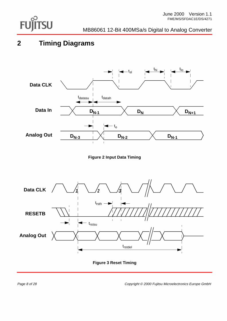
A RESETB pin is provided, which when taken low allows the device to be reset and placed in a low powerstate. The device must be clocked in order to reset the device, and RESETB must be held low for aminimum of two clock cycles. See Figure 3.
On power up the device must be reset before it is operational. Configuration changes require a device resetto be performed.
June 2000 Version 1.1FME/MS/SFDAC1E/DS/4271
MB86061 12-Bit 400MSa/s Digital to Analog Converter
Page 8 of 28 Copyright © 2000 Fujitsu Microelectronics Europe GmbH
2 Timing Diagrams
Figure 2 Input Data Timing
Figure 3 Reset Timing
Data CLK
Analog Out
Data In DN-1 DN DN+1
DN-2DN-3 DN-1
to
tslthi tlo
tdatasu tdatah
Data CLK
Analog Out
RESETB
trstsu
trstdel
trsth
1 2 3
June 2000 Version 1.1FME/MS/SFDAC1E/DS/4271
MB86061 12-Bit 400MSa/s Digital to Analog Converter
Copyright © 2000 Fujitsu Microelectronics Europe GmbH Page 9 of 28
3 Electrical Specifications
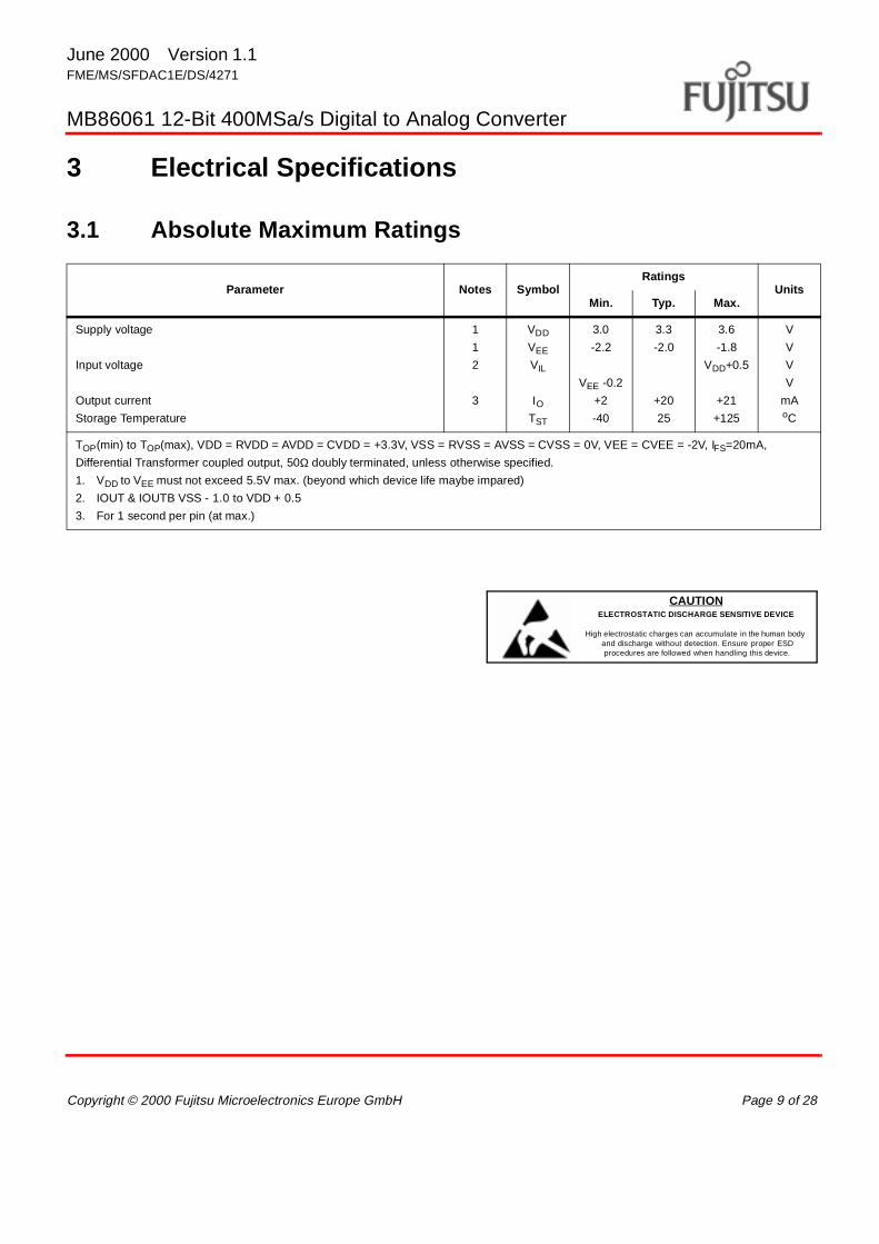
3.1 Absolute Maximum Ratings
Parameter Notes SymbolRatings
UnitsMin. Typ. Max.
Supply voltage
Input voltage
Output current
Storage Temperature
1
1
2
3
VDD
VEE
VIL
ΙOTST
3.0
-2.2
VEE -0.2
+2
-40
3.3
-2.0
+20
25
3.6
-1.8
VDD+0.5
+21
+125
V
V
V
V
mAoC
TOP(min) to TOP(max), VDD = RVDD = AVDD = CVDD = +3.3V, VSS = RVSS = AVSS = CVSS = 0V, VEE = CVEE = -2V, IFS=20mA,
Differential Transformer coupled output, 50Ω doubly terminated, unless otherwise specified.
1. VDD to VEE must not exceed 5.5V max. (beyond which device life maybe impared)
2. IOUT & IOUTB VSS - 1.0 to VDD + 0.5
3. For 1 second per pin (at max.)
CAUTIONELECTROSTATIC DISCHARGE SEN SITIVE DEVICE
High electrostatic charges can accumulate in the human body and discharge without detection. Ensure proper ESD procedures are followed when handling this device.
June 2000 Version 1.1FME/MS/SFDAC1E/DS/4271
MB86061 12-Bit 400MSa/s Digital to Analog Converter
Page 10 of 28 Copyright © 2000 Fujitsu Microelectronics Europe GmbH
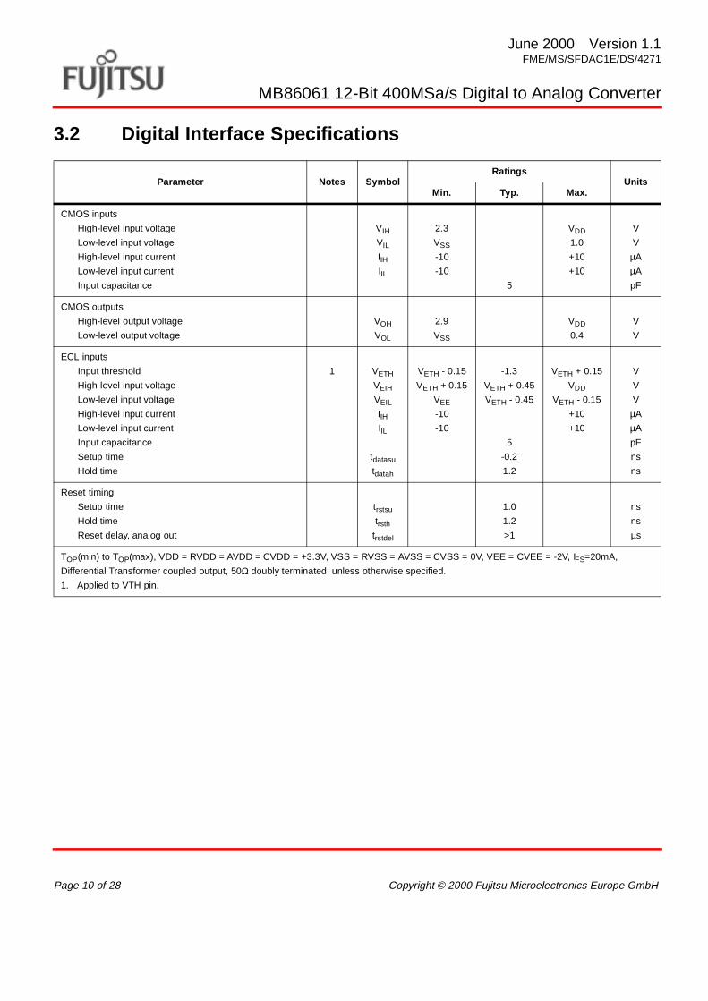
3.2 Digital Interface Specifications
Parameter Notes SymbolRatings
UnitsMin. Typ. Max.
CMOS inputs
High-level input voltage
Low-level input voltage
High-level input current
Low-level input current
Input capacitance
VIH
VIL
IIHIIL
2.3
VSS
-10
-10
5
VDD
1.0
+10
+10
V
V
µA
µA
pF
CMOS outputs
High-level output voltage
Low-level output voltage
VOH
VOL
2.9
VSS
VDD
0.4
V
V
ECL inputs
Input threshold
High-level input voltage
Low-level input voltage
High-level input current
Low-level input current
Input capacitance
Setup time
Hold time
1 VETH
VEIH
VEIL
IIHIIL
tdatasu
tdatah
VETH - 0.15
VETH + 0.15
VEE
-10
-10
-1.3
VETH + 0.45
VETH - 0.45
5
-0.2
1.2
VETH + 0.15
VDD
VETH - 0.15
+10
+10
V
V
V
µA
µA
pF
ns
ns
Reset timing
Setup time
Hold time
Reset delay, analog out
trstsu
trsth
trstdel
1.0
1.2
>1
ns
ns
µs
TOP(min) to TOP(max), VDD = RVDD = AVDD = CVDD = +3.3V, VSS = RVSS = AVSS = CVSS = 0V, VEE = CVEE = -2V, IFS=20mA,
Differential Transformer coupled output, 50Ω doubly terminated, unless otherwise specified.
1. Applied to VTH pin.
June 2000 Version 1.1FME/MS/SFDAC1E/DS/4271
MB86061 12-Bit 400MSa/s Digital to Analog Converter
Copyright © 2000 Fujitsu Microelectronics Europe GmbH Page 11 of 28
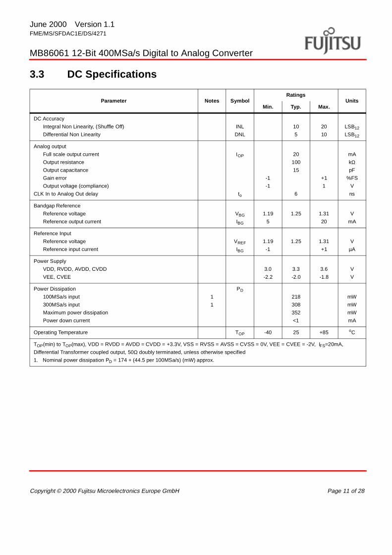
3.3 DC Specifications
Parameter Notes SymbolRatings
UnitsMin. Typ. Max.
DC Accuracy
Integral Non Linearity, (Shuffle Off)
Differential Non Linearity
INL
DNL
10
5
20
10
LSB12
LSB12
Analog output
Full scale output current
Output resistance
Output capacitance
Gain error
Output voltage (compliance)
CLK In to Analog Out delay
ΙOP
to
-1
-1
20
100
15
6
+1
1
mA
kΩpF
%FS
V
ns
Bandgap Reference
Reference voltage
Reference output current
VBG
IBG
1.19
5
1.25 1.31
20
V
mA
Reference Input
Reference voltage
Reference input current
VREF
IBG
1.19
-1
1.25 1.31
+1
V
µA
Power Supply
VDD, RVDD, AVDD, CVDD
VEE, CVEE
3.0
-2.2
3.3
-2.0
3.6
-1.8
V
V
Power Dissipation
100MSa/s input
300MSa/s input
Maximum power dissipation
Power down current
1
1
PD
218
308
352
<1
mW
mW
mW
mA
Operating Temperature TOP -40 25 +85 oC
TOP(min) to TOP(max), VDD = RVDD = AVDD = CVDD = +3.3V, VSS = RVSS = AVSS = CVSS = 0V, VEE = CVEE = -2V, IFS=20mA,
Differential Transformer coupled output, 50Ω doubly terminated, unless otherwise specified
1. Nominal power dissipation PD = 174 + (44.5 per 100MSa/s) (mW) approx.
June 2000 Version 1.1FME/MS/SFDAC1E/DS/4271
MB86061 12-Bit 400MSa/s Digital to Analog Converter
Page 12 of 28 Copyright © 2000 Fujitsu Microelectronics Europe GmbH
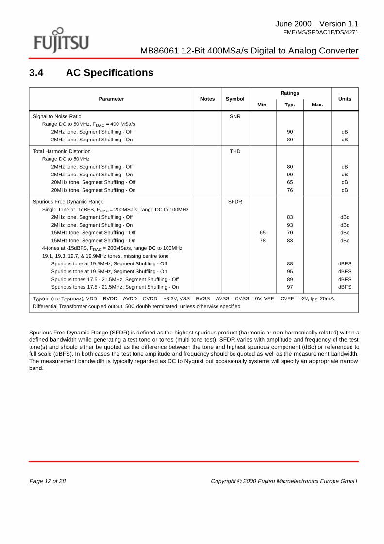
3.4 AC Specifications
Spurious Free Dynamic Range (SFDR) is defined as the highest spurious product (harmonic or non-harmonically related) within adefined bandwidth while generating a test tone or tones (multi-tone test). SFDR varies with amplitude and frequency of the testtone(s) and should either be quoted as the difference between the tone and highest spurious component (dBc) or referenced tofull scale (dBFS). In both cases the test tone amplitude and frequency should be quoted as well as the measurement bandwidth.The measurement bandwidth is typically regarded as DC to Nyquist but occasionally systems will specify an appropriate narrowband.
Parameter Notes SymbolRatings
UnitsMin. Typ. Max.
Signal to Noise Ratio
Range DC to 50MHz, FDAC = 400 MSa/s
2MHz tone, Segment Shuffling - Off
2MHz tone, Segment Shuffling - On
SNR
90
80
dB
dB
Total Harmonic Distortion
Range DC to 50MHz
2MHz tone, Segment Shuffling - Off
2MHz tone, Segment Shuffling - On
20MHz tone, Segment Shuffling - Off
20MHz tone, Segment Shuffling - On
THD
80
90
65
76
dB
dB
dB
dB
Spurious Free Dynamic Range
Single Tone at -1dBFS, FDAC = 200MSa/s, range DC to 100MHz
2MHz tone, Segment Shuffling - Off
2MHz tone, Segment Shuffling - On
15MHz tone, Segment Shuffling - Off
15MHz tone, Segment Shuffling - On
4-tones at -15dBFS, FDAC = 200MSa/s, range DC to 100MHz
19.1, 19.3, 19.7, & 19.9MHz tones, missing centre tone
Spurious tone at 19.5MHz, Segment Shuffling - Off
Spurious tone at 19.5MHz, Segment Shuffling - On
Spurious tones 17.5 - 21.5MHz, Segment Shuffling - Off
Spurious tones 17.5 - 21.5MHz, Segment Shuffling - On
SFDR
65
78
83
93
70
83
88
95
89
97
dBc
dBc
dBc
dBc
dBFS
dBFS
dBFS
dBFS
TOP(min) to TOP(max), VDD = RVDD = AVDD = CVDD = +3.3V, VSS = RVSS = AVSS = CVSS = 0V, VEE = CVEE = -2V, IFS=20mA,
Differential Transformer coupled output, 50Ω doubly terminated, unless otherwise specified

June 2000 Version 1.1FME/MS/SFDAC1E/DS/4271
MB86061 12-Bit 400MSa/s Digital to Analog Converter
Copyright © 2000 Fujitsu Microelectronics Europe GmbH Page 13 of 28
3.5 Clock Specifications
Parameter Notes SymbolRatings
UnitsMin. Typ. Max.
Maximum DAC Conversion rate
VDD < 3.3V
VDD ≥ 3.3V
FDAC 350
400
MSa/s
MSa/s
Clock in
Low time
High time
Slew rate for minimum wide-band jitter
Common mode input voltage
Signal level (differential) 1
tLO
tHI
tSL
Vcm
1
1
0.5
0
100
VSS - 1.25
ns
ns
V/ns
V
mV
TOP(min) to TOP(max), VDD = RVDD = AVDD = CVDD = +3.3V, VSS = RVSS = AVSS = CVSS = 0V, VEE = CVEE = -2V, IFS=20mA,
Differential Transformer coupled output, 50Ω doubly terminated, unless otherwise specified
1. Ensure that slew rate specifications are observed

June 2000 Version 1.1FME/MS/SFDAC1E/DS/4271
MB86061 12-Bit 400MSa/s Digital to Analog Converter
Page 14 of 28 Copyright © 2000 Fujitsu Microelectronics Europe GmbH
3.6 Typical Performance Characterisation Graphs
Single Tone Spurious Free Dynamic Range
Figure 4 Single Tone SFDR Performance
Multi-tone test, 4 tones, 200kHz channelspacing, missing centre tone
Figure 5 Multi-tone Performance
60
65
70
75
80
85
90
95
0 10 20 30 40
Generated Frequency(MHz)
SF
DR
(dB
c)
200MSa/s DAC RateAmplitude = -1dBFS
Shuffle On
Shuffle Off
-120
-100
-80
-60
-40
-20
0
17 18 19 20 21 22
Generated Frequency(MHz)
Am
plitu
de(d
BF
S)
200MSa/s Input Data RateShuffle On4 Tones each at -15dBFS
June 2000 Version 1.1FME/MS/SFDAC1E/DS/4271
MB86061 12-Bit 400MSa/s Digital to Analog Converter
Copyright © 2000 Fujitsu Microelectronics Europe GmbH Page 15 of 28
4 Application Notes
4.1 Power & Ground Plane Regions
The following guidelines are suggested to obtain the specified performance. Any departure from theserecommendations should be investigated to confirm that performance in the application is acceptable.
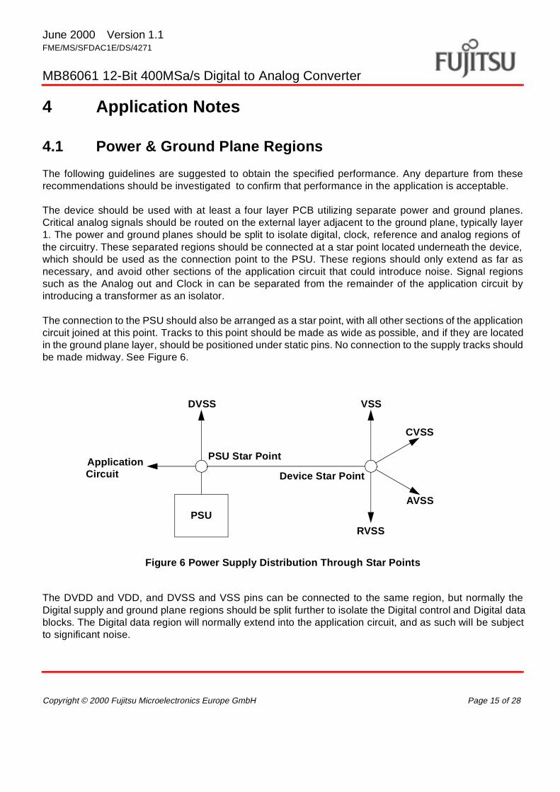
The device should be used with at least a four layer PCB utilizing separate power and ground planes.Critical analog signals should be routed on the external layer adjacent to the ground plane, typically layer1. The power and ground planes should be split to isolate digital, clock, reference and analog regions ofthe circuitry. These separated regions should be connected at a star point located underneath the device,which should be used as the connection point to the PSU. These regions should only extend as far asnecessary, and avoid other sections of the application circuit that could introduce noise. Signal regionssuch as the Analog out and Clock in can be separated from the remainder of the application circuit byintroducing a transformer as an isolator.
The connection to the PSU should also be arranged as a star point, with all other sections of the applicationcircuit joined at this point. Tracks to this point should be made as wide as possible, and if they are locatedin the ground plane layer, should be positioned under static pins. No connection to the supply tracks shouldbe made midway. See Figure 6.
Figure 6 Power Supply Distribution Thr ough Star Points
The DVDD and VDD, and DVSS and VSS pins can be connected to the same region, but normally theDigital supply and ground plane regions should be split further to isolate the Digital control and Digital datablocks. The Digital data region will normally extend into the application circuit, and as such will be subjectto significant noise.
PSU
VSS
CVSS
AVSS
RVSS
DVSS
ApplicationCircuit
PSU Star Point
Device Star Point
June 2000 Version 1.1FME/MS/SFDAC1E/DS/4271
MB86061 12-Bit 400MSa/s Digital to Analog Converter
Page 16 of 28 Copyright © 2000 Fujitsu Microelectronics Europe GmbH
Another main reason for splitting the digital data ground plane from the main digital ground is that whenusing a remote data generator (e.g. a benchtop pattern or data generator) there is a tendency for noise tobe injected on the data ground by the equipment. This is significant because the data rate is high, the databus is wide, and it is correlated with the signal so can cause spurious tones which degrade SFDR. Thecoupling mechanism is from the fast-slewing data inputs via the capacitance of the input pins/pads/protection diodes into the internal circuits. The transient currents through these parasitics can be severalhundred milliamps. For this reason, it is recommended that this region is not connected to the device starpoint but to the PSU star point directly.
The input data bus and supplies are only used for the input section of the device, so noise in this regioncannot couple into the DAC core. The main digital supply connects to the digital circuits inside the DAC,including those inside the DAC core. The control inputs can use this supply because they toggle moreslowly (if at all) and are not correlated with the data. The analog sections (Analog, Clock and Reference)have separate supply connections as transition dependant currents from the digital sections will causedelay modulation in the clock path, and amplitude modulation in the analog output section.
Each supply should be decoupled, producing a low impedance shunt at high frequency. The Digital,Analog, Clock and Reference sections can be connected directly to the device star point, but preferablythrough a small inductor. If a fully split power (VDD) plane is not desired, then as a minimum only theground plane need be split as described. However it is very important to isolate the I/O supply (DVDD) fromall other supplies in some way, possibly feeding the supply through a low-R resistor or ferrite bead. Thiswill help to filter out noise.
If the data (signal) and control lines are coming from the same device (e.g. an ASIC), then generally thiswould have been designed to support separate supply and ground pins for the digital data bus anyway.The ground plane at the generating device then becomes the "star point" for the data, requiring cuts in theground/supply planes on either side of the data bus, and looping under the DAC. The digital datadecoupling at the DAC should also be inside this loop. This gives a "U" shaped cut in the planes with theopen end at the data source (with decoupling) and the closed end at the DAC (with decoupling). All thedata return currents will then be confined inside this "U", and so none of them can couple into the analogground planes to degrade SFDR. It may be advisable to bury the digital data bus tracks on an internal layer,with data ground planes above, below and either side of the tracks (the ground layers connected togetherwith a row of vias) to shield against RF radiation.
Figure 7 shows these principles applied to the ground plane of an application board. The pad on the leftrepresents the PSU star point, and the pad in the center represents the device star point. These pointscould be realized with a via, so that the connection from the PSU out to other star points could be made onanother layer if necessary. The positioning of the plane breaks are also shown. The breaks in the planesbetween each section should mark the boundary of that section. It is very important to ensure that thereare no tracks crossing these boundaries, or any splits in the planes that tracks must cross, as this will createcurrent loops within the plane itself.
The power supply track regions, PSU and Opt. PSU are shown extending to either side of the device forreference purposes. Only one track region would normally be used. If the PSU region is not required, thenthe region should be merged with the Digital region.

June 2000 Version 1.1FME/MS/SFDAC1E/DS/4271
MB86061 12-Bit 400MSa/s Digital to Analog Converter
Copyright © 2000 Fujitsu Microelectronics Europe GmbH Page 17 of 28
Figure 7 Recommended Ground Plane Splits
4.2 Power Supplies
Only one clean low-impedance power supply is required. Power distribution should be organized as shownin Figure 6, with a main star point at the PSU supplying the data (DVDD/DVSS) block, with a secondarydevice star point supplying the Digital, Analog, Clock and Reference blocks. If this supply is used to supplyany other circuits, they must not introduce any modulation onto the supply, or SFDR will be degraded.
If the impedance of the supply is not low enough to prevent modulation by the currents drawn by the datasource, then a separate supply for the Data source should be used. If the Digital, Analog, Clock andReference block supply is still not low enough impedance to prevent power supply modulation beingintroduced by the Digital block, then a further supply for the Analog block alone must be introduced.
Bulk decoupling of around 100uF at the power supply star point is recommended to remove any lowfrequency ripple. Smaller value decoupling of around 1 to 10uF at the device star point is recommended toapply a low impedance shunt at high frequency.
N/CN/CVSSVDDDSUBCSUBRESETBCVDDCVSSCLKCVEECLKB
RV
SS
RV
DD
AVD
DAV
SS
IOU
TBIO
UTB
AVD
D
AVS
S
AVD
D
AVS
S
AVD
DC
VD
DC
VS
S
D2
DV
SS
D3
D4
DV
DD
D5
D6
DV
SS
D7
D8
DV
DD
D9
VE
E
VDD
D11VSS
D10
VSSVDD
TWOCN/C
VDDVSS
DSUBASUB
SHUF1SHUF0
RVSSBGAPVREFRREF
Pin #1
D1
VE
E
D0VTH
IOU
TIO
UT
AVS
S
VE
E
R ef. RegionAnalog reg ion
Clock region
Digita l reg ion
Dig ita l Data region
PSU region
Application region
Opt. PSU region
June 2000 Version 1.1FME/MS/SFDAC1E/DS/4271
MB86061 12-Bit 400MSa/s Digital to Analog Converter
Page 18 of 28 Copyright © 2000 Fujitsu Microelectronics Europe GmbH
Power supply tracks should be kept as short and wide as possible. The ground and supply tracks shouldrun adjacent to each other for as far as possible, whilst avoiding all signal tracks that may couple noise intothe supply.
4.3 Decoupling
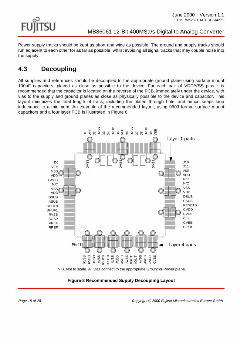
All supplies and references should be decoupled to the appropriate ground plane using surface mount100nF capacitors, placed as close as possible to the device. For each pair of VDD/VSS pins it isrecommended that the capacitor is located on the reverse of the PCB, immediately under the device, withvias to the supply and ground planes as close as physically possible to the device and capacitor. Thislayout minimizes the total length of track, including the plated through hole, and hence keeps loopinductance to a minimum. An example of the recommended layout, using 0603 format surface mountcapacitors and a four layer PCB is illustrated in Figure 8.
Figure 8 Recommended Supply Decoupling Layout
Pin #1 Layer 4 pads
Layer 1 pads
N.B. Not to scale. All vias connect to the appropriate Ground or Power plane.
N/CN/CVSSVDDDSUBCSUBRESETBCVDDCVSSCLKCVEECLKB
RV
SS
RV
DD
AVD
DAV
SS
IOU
TB
IOU
TB
AVD
D
AVS
S
AVD
D
AVS
S
AVD
D
CV
DD
CV
SS
D2
DV
SS
D3
D4
DV
DD
D5
D6
DV
SS
D7
D8
DV
DD
D9
VE
E
VDD
D11VSS
D10
VSSVDD
TWOCN/C
VDDVSS
DSUBASUB
SHUF1SHUF0
RVSSBGAPVREFRREF
D1
VE
E
D0VTH
IOU
TIO
UT
AVS
SV
EE
DV
SS
DV
SS
DV
SS
June 2000 Version 1.1FME/MS/SFDAC1E/DS/4271
MB86061 12-Bit 400MSa/s Digital to Analog Converter
Copyright © 2000 Fujitsu Microelectronics Europe GmbH Page 19 of 28
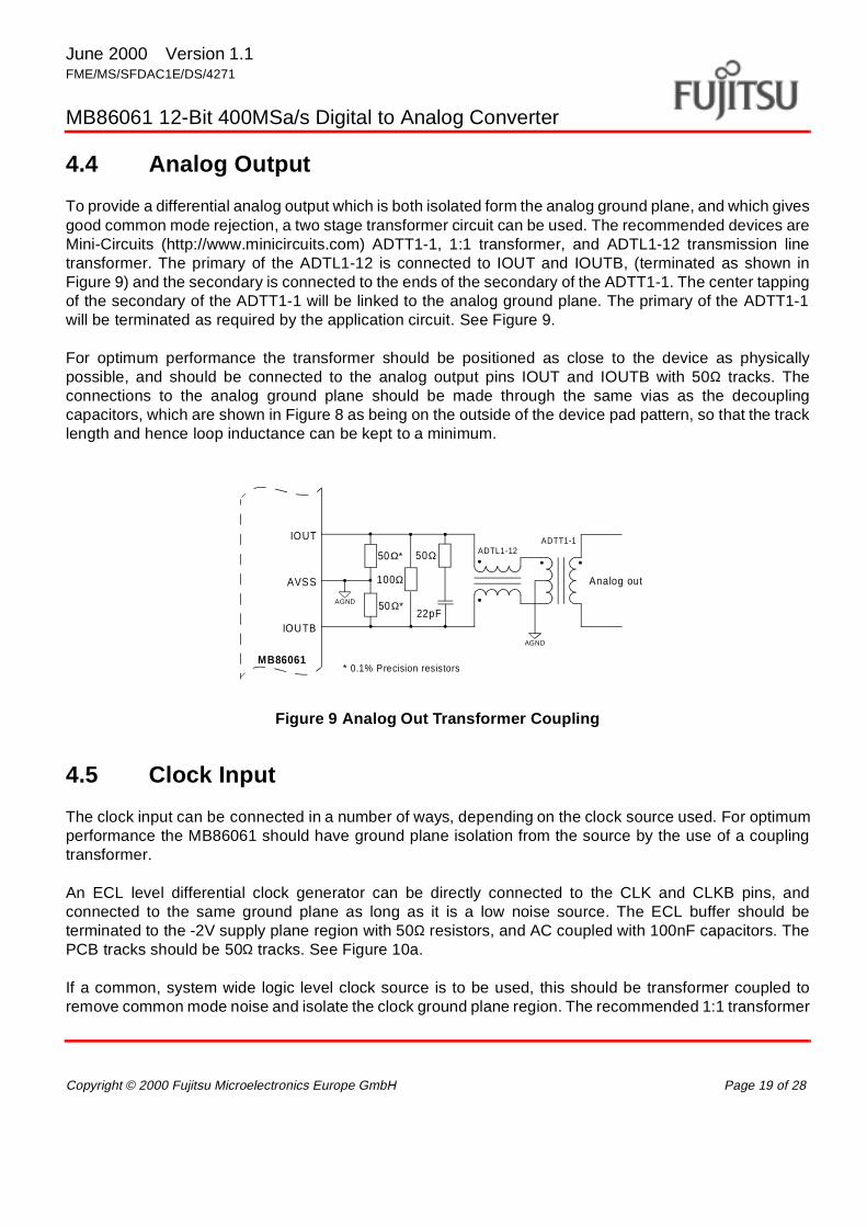
4.4 Analog Output
To provide a differential analog output which is both isolated form the analog ground plane, and which givesgood common mode rejection, a two stage transformer circuit can be used. The recommended devices areMini-Circuits (http://www.minicircuits.com) ADTT1-1, 1:1 transformer, and ADTL1-12 transmission linetransformer. The primary of the ADTL1-12 is connected to IOUT and IOUTB, (terminated as shown inFigure 9) and the secondary is connected to the ends of the secondary of the ADTT1-1. The center tappingof the secondary of the ADTT1-1 will be linked to the analog ground plane. The primary of the ADTT1-1will be terminated as required by the application circuit. See Figure 9.
For optimum performance the transformer should be positioned as close to the device as physicallypossible, and should be connected to the analog output pins IOUT and IOUTB with 50Ω tracks. Theconnections to the analog ground plane should be made through the same vias as the decouplingcapacitors, which are shown in Figure 8 as being on the outside of the device pad pattern, so that the tracklength and hence loop inductance can be kept to a minimum.
Figure 9 Analog Out Transformer Coupling
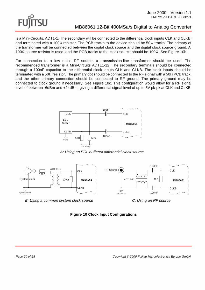
4.5 Clock Input
The clock input can be connected in a number of ways, depending on the clock source used. For optimumperformance the MB86061 should have ground plane isolation from the source by the use of a couplingtransformer.
An ECL level differential clock generator can be directly connected to the CLK and CLKB pins, andconnected to the same ground plane as long as it is a low noise source. The ECL buffer should beterminated to the -2V supply plane region with 50Ω resistors, and AC coupled with 100nF capacitors. ThePCB tracks should be 50Ω tracks. See Figure 10a.
If a common, system wide logic level clock source is to be used, this should be transformer coupled toremove common mode noise and isolate the clock ground plane region. The recommended 1:1 transformer
IOUT
AVSS
IOUTB
100Ω Analog out
ADTL1-12
MB86061
AGND
50Ω∗
50Ω∗
AGND
50Ω
22pF
ADTT1-1
∗ 0.1% Precision resistors
June 2000 Version 1.1FME/MS/SFDAC1E/DS/4271
MB86061 12-Bit 400MSa/s Digital to Analog Converter
Page 20 of 28 Copyright © 2000 Fujitsu Microelectronics Europe GmbH
is a Mini-Circuits, ADT1-1. The secondary will be connected to the differential clock inputs CLK and CLKB,and terminated with a 100Ω resistor. The PCB tracks to the device should be 50Ω tracks. The primary ofthe transformer will be connected between the digital clock source and the digital clock source ground. A100Ω source resistor is used, and the PCB tracks to the clock source should be 100Ω. See Figure 10b.
For connection to a low noise RF source, a transmission-line transformer should be used. Therecommended transformer is a Mini-Circuits ADTL1-12. The secondary terminals should be connectedthrough a 100nF capacitor to the differential clock inputs CLK and CLKB. The clock inputs should beterminated with a 50Ω resistor. The primary dot should be connected to the RF signal with a 50Ω PCB track,and the other primary connection should be connected to RF ground. The primary ground may beconnected to clock ground if necessary. See Figure 10c. This configuration would allow for a RF signallevel of between -6dBm and +24dBm, giving a differential signal level of up to 5V pk-pk at CLK and CLKB.
Figure 10 Clock Input Configurations
100nF
50Ω
RF Source
ADTL1-12
System Ground
CLK
CLKB
MB86061
100Ω
System clock
B: Using a common system clock source
CLK
CLKB
MB86061
RF Ground 100nF
C: Using an RF source
100Ω
ADTT1-1
100nF
50Ω
CLK
CLKB
MB86061
CGND
100nF50Ω
-2V Supply
CLK
CLKB
ECLBuffer
A: Using an ECL buffered differential clock source
June 2000 Version 1.1FME/MS/SFDAC1E/DS/4271
MB86061 12-Bit 400MSa/s Digital to Analog Converter
Copyright © 2000 Fujitsu Microelectronics Europe GmbH Page 21 of 28
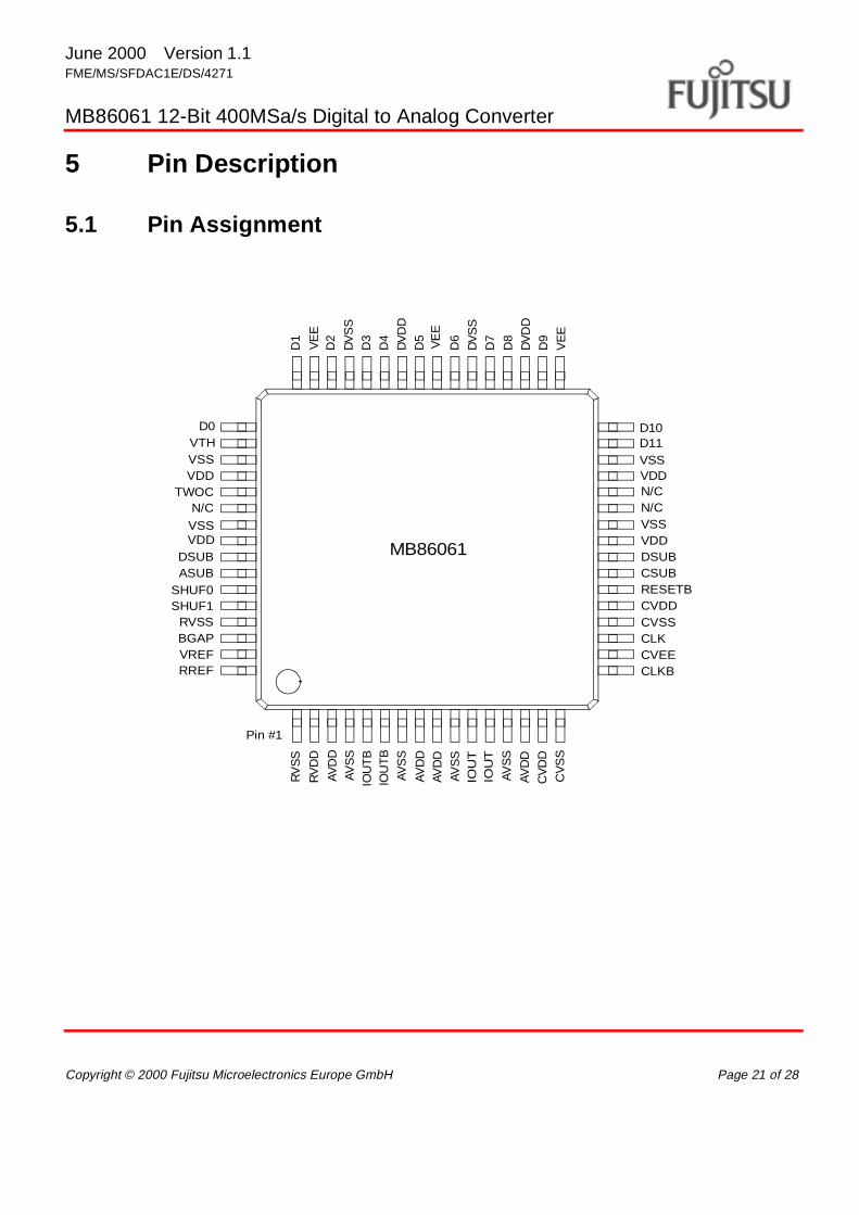
5 Pin Description
5.1 Pin Assignment
N/CN/CVSSVDDDSUBCSUBRESETBCVDDCVSSCLKCVEECLKB
RV
SS
RV
DD
AVD
DAV
SS
IOU
TB
IOU
TB
AVD
D
AVS
S
AVD
D
AVS
S
AVD
D
CV
DD
CV
SS
D2
DV
SS
D3
D4
DV
DD
D5
D6
DV
SS
D7
D8
DV
DD
D9
VE
E
VDD
D11VSS
D10
VSSVDD
TWOCN/C
VDDVSS
DSUBASUB
SHUF1SHUF0
RVSSBGAPVREFRREF
Pin #1
D1
VE
E
MB86061
D0VTH
IOU
TIO
UT
AVS
S
VE
E
June 2000 Version 1.1FME/MS/SFDAC1E/DS/4271
MB86061 12-Bit 400MSa/s Digital to Analog Converter
Page 22 of 28 Copyright © 2000 Fujitsu Microelectronics Europe GmbH
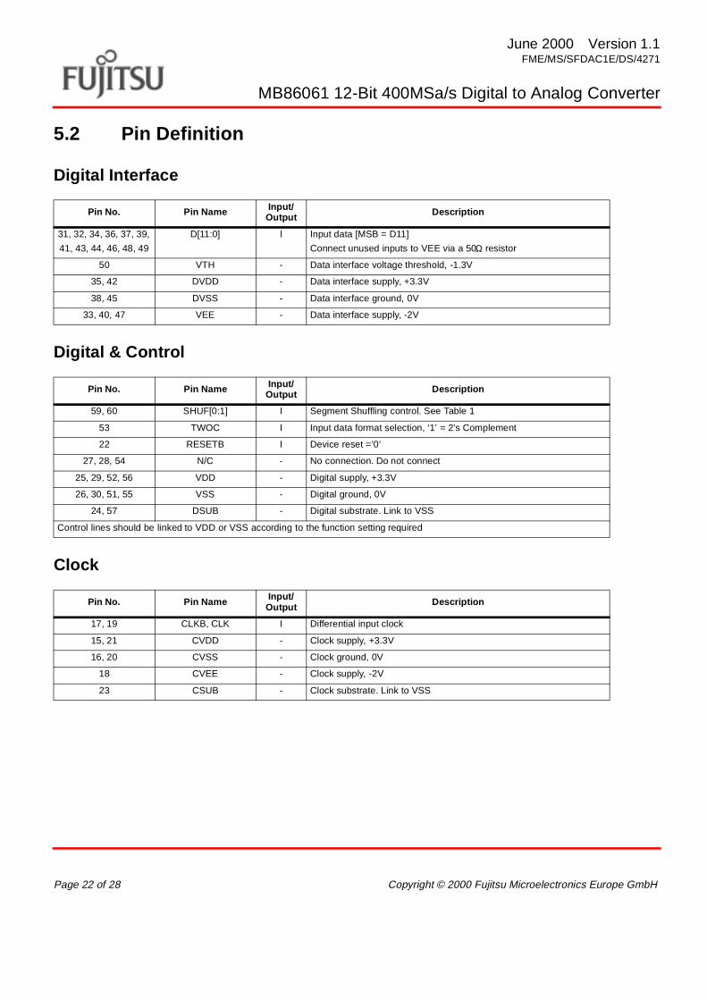
5.2 Pin Definition
Digital Interface
Digital & Control
Clock
Pin No. Pin Name Input/Output Description
31, 32, 34, 36, 37, 39,
41, 43, 44, 46, 48, 49
D[11:0] I Input data [MSB = D11]
Connect unused inputs to VEE via a 50Ω resistor
50 VTH - Data interface voltage threshold, -1.3V
35, 42 DVDD - Data interface supply, +3.3V
38, 45 DVSS - Data interface ground, 0V
33, 40, 47 VEE - Data interface supply, -2V
Pin No. Pin Name Input/Output Description
59, 60 SHUF[0:1] I Segment Shuffling control. See Table 1
53 TWOC I Input data format selection, ‘1’ = 2’s Complement
22 RESETB I Device reset =’0’
27, 28, 54 N/C - No connection. Do not connect
25, 29, 52, 56 VDD - Digital supply, +3.3V
26, 30, 51, 55 VSS - Digital ground, 0V
24, 57 DSUB - Digital substrate. Link to VSS
Control lines should be linked to VDD or VSS according to the function setting required
Pin No. Pin Name Input/Output Description
17, 19 CLKB, CLK I Differential input clock
15, 21 CVDD - Clock supply, +3.3V
16, 20 CVSS - Clock ground, 0V
18 CVEE - Clock supply, -2V
23 CSUB - Clock substrate. Link to VSS
June 2000 Version 1.1FME/MS/SFDAC1E/DS/4271
MB86061 12-Bit 400MSa/s Digital to Analog Converter
Copyright © 2000 Fujitsu Microelectronics Europe GmbH Page 23 of 28
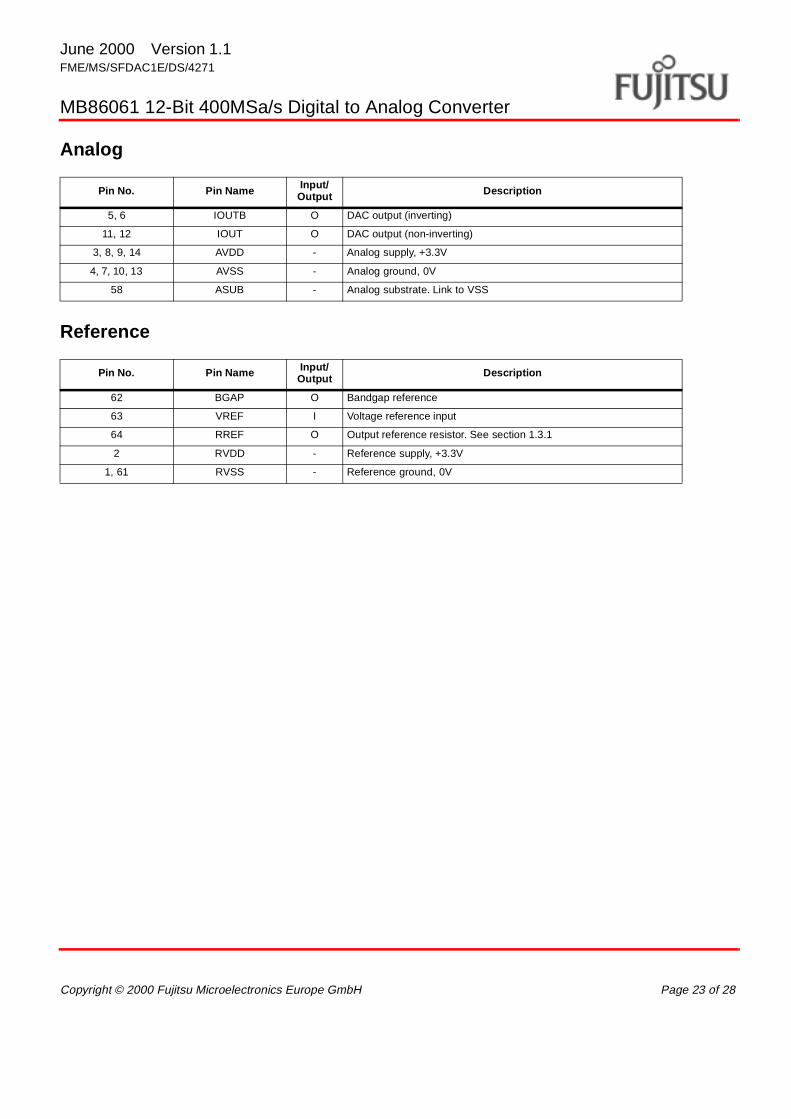
Analog
Reference
Pin No. Pin Name Input/Output Description
5, 6 IOUTB O DAC output (inverting)
11, 12 IOUT O DAC output (non-inverting)
3, 8, 9, 14 AVDD - Analog supply, +3.3V
4, 7, 10, 13 AVSS - Analog ground, 0V
58 ASUB - Analog substrate. Link to VSS
Pin No. Pin Name Input/Output Description
62 BGAP O Bandgap reference
63 VREF I Voltage reference input
64 RREF O Output reference resistor. See section 1.3.1
2 RVDD - Reference supply, +3.3V
1, 61 RVSS - Reference ground, 0V
June 2000 Version 1.1FME/MS/SFDAC1E/DS/4271
MB86061 12-Bit 400MSa/s Digital to Analog Converter
Page 24 of 28 Copyright © 2000 Fujitsu Microelectronics Europe GmbH
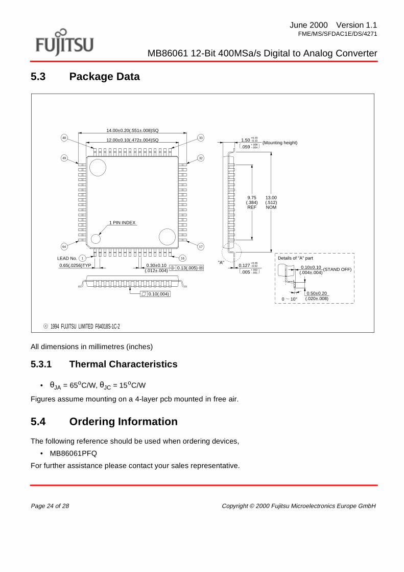
5.3 Package Data
All dimensions in millimetres (inches)
5.3.1 Thermal Characteristics
• θJA = 65oC/W, θJC = 15oC/W
Figures assume mounting on a 4-layer pcb mounted in free air.
5.4 Ordering Information
The following reference should be used when ordering devices,
• MB86061PFQ
For further assistance please contact your sales representative.
C 1994 FUJITSU LIMITED F64018S-1C-2
0.13(.005) M
0.10(.004)
1 PIN INDEX
.005 –.001+.002
–0.02+0.05
0.127
.059 –.004+.008
–0.10+0.20
1.50
"A"Details of "A" part
0 10°0.50±0.20
0.10±0.10(.004±.004)
(.020±.008)
14.00±0.20(.551±.008)SQ
12.00±0.10(.472±.004)SQ
0.65(.0256)TYP 0.30±0.10(.012±.004)
9.75 13.00(.384)REF
(.512)NOM
1 16
17
32
3348
49
64
(STAND OFF)
LEAD No.
(Mounting height)
June 2000 Version 1.1FME/MS/SFDAC1E/DS/4271
MB86061 12-Bit 400MSa/s Digital to Analog Converter
Copyright © 2000 Fujitsu Microelectronics Europe GmbH Page 25 of 28
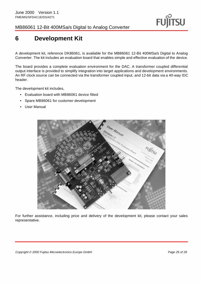
6 Development Kit
A development kit, reference DK86061, is available for the MB86061 12-Bit 400MSa/s Digital to AnalogConverter. The kit includes an evaluation board that enables simple and effective evaluation of the device.
The board provides a complete evaluation environment for the DAC. A transformer coupled differentialoutput interface is provided to simplify integration into target applications and development environments.An RF clock source can be connected via the transformer coupled input, and 12-bit data via a 40-way IDCheader.
The development kit includes,
• Evaluation board with MB86061 device fitted
• Spare MB86061 for customer development
• User Manual
For further assistance, including price and delivery of the development kit, please contact your salesrepresentative.
June 2000 Version 1.1FME/MS/SFDAC1E/DS/4271
MB86061 12-Bit 400MSa/s Digital to Analog Converter
Page 26 of 28 Copyright © 2000 Fujitsu Microelectronics Europe GmbH
Notes:
June 2000 Version 1.1FME/MS/SFDAC1E/DS/4271
MB86061 12-Bit 400MSa/s Digital to Analog Converter
Copyright © 2000 Fujitsu Microelectronics Europe GmbH Page 27 of 28
Notes:
June 2000 Version 1.1FME/MS/SFDAC1E/DS/4271
MB86061 12-Bit 400MSa/s Digital to Analog Converter
Page 28 of 28 Copyright © 2000 Fujitsu Microelectronics Europe GmbH
FME/MS/SFDAC1E/DS/4271 - 1.1
Worldwide Headquarters
Japan Fujitsu Limited Asia Fujitsu Microelectronics Asia Pte Limited
Tel:Fax:
+81 44 754 3753+81 44 754 3329
1015 Kamikodanaka 4-1-1Nakahara-kuKawasaki-shiKanagawa-ken 211-88Japan
Tel:Fax:
+65 281 0770+65 281 0220
151 Lorong Chuan#05-08 New Tech ParkSingapore 556741
http://www.fujitsu.co.jp/ http://www.fmap.com.sg/
USA Fujitsu Microelectronics Inc Europe Fujitsu Microlectronics Europe GmbH
Tel:Fax:
+1 408 922 9000+1 408 922 9179
3545 North First StreetSan Jose CA 95134-1804USA
Tel:Fax:
+49 6103 6900+49 6103 690122
Am Siebenstein 6-10D-63303 Dreieich-BuchschlagGermany
Tel:Fax:
+1 800 866 8608+1 408 922 9179
Customer Response CenterMon-Fri: 7am-5pm (PST)
http://www.fujitsu-fme.com/
http://www.fujitsumicro.com/
The contents of this document are subject to change without notice. Customers are advised to consult with FUJITSU sales representatives before ordering.
The information and circuit diagrams in this document presented as examples of semiconductor device applications, and are not intended to be incorporated in devices for actual use. Also, FUJITSU is unable to assume responsibility for infringement of any patent rights or other rights of third parties arising from the use of this information or circuit diagrams.
FUJITSU semiconductor devices are intended for use in standard applications (computers, office automation and other office equipment, industrial, communications, and measurement equipment, personal or household devices, etc.). CAUTION: Customers considering the use of our products in special applications where failure or abnormal operation may directly affect human lives or cause physical injury or property damage, or where extremely high levels of reliability are demanded (such as aerospace systems, atomic energy controls, sea floor repeaters, vehicle operating controls, medical devices for life support, etc.) are requested to consult with FUJITSU sales representatives before such use. The company will not be responsible for damages arising from such use without prior approval.
Any semiconductor devices have inherently a certain rate of failure. You must protect against injury, damage or loss from such failures by incorporating safety design measures into your facility and equipment such as redundancy, fire protection, and prevention of over-current levels and other abnormal operating conditions.
If any products described in this document represent goods or technologies subject to certain restrictions on export under the Foreign Exchange and Foreign Trade Control Law of Japan, the prior authorization by Japanese government should be required for export of those products from Japan.


![Atmel ATmega16U4, ATmega32U4 Datasheet Summaryww1.microchip.com/.../Atmel-7766-8-bit-AVR-ATmega16U4-32U4_Sum… · DATASHEET SUMMARY. ATmega16U4/32U4 [DATASHEET] ... The AVR core](https://img.pdfslide.net/doc/110x75/5aeada877f8b9a66258c91a3/atmel-atmega16u4-atmega32u4-datasheet-datasheet-summary-atmega16u432u4-datasheet.jpg)