Embed Size (px)
Citation preview
TO-220FP
IPAK
TO-220
DPAK
Features• Output current to 0.5 A• Output voltages of 5; 6; 8; 9; 10; 12; 15; 24 V• Thermal overload protection• Short circuit protection• Output transition SOA protection• Output voltage tolerance: 2 % (AB and AC versions) or 4 % (C version)• Guaranteed in extended temperature range
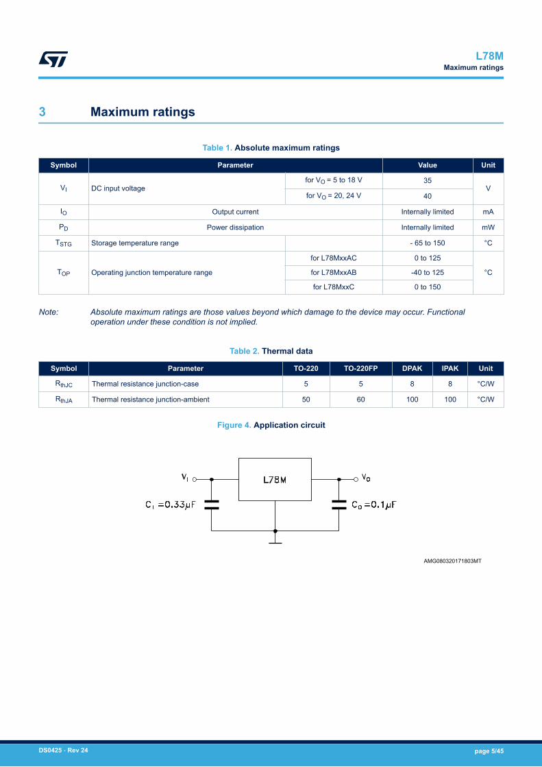
DescriptionThe L78M series of three-terminal positive regulators is available in TO-220,TO-220FP, DPAK and IPAK packages and with several fixed output voltages, makingit useful in a wide range of applications. These regulators can provide local on-cardregulation, eliminating the distribution problems associated with single pointregulation. Each type employs internal current limiting, thermal shutdown and safearea protection, resulting it essentially indestructible. If adequate heat sinking isprovided, they can deliver over 0.5 A output current. Although designed primarily asfixed voltage regulators, these devices can be used with external components toobtain adjustable voltage and currents.
Maturity status link
L78M
Precision 500 mA regulators
L78M
Datasheet
DS0425 - Rev 24 - September 2020For further information contact your local STMicroelectronics sales office.
www.st.com
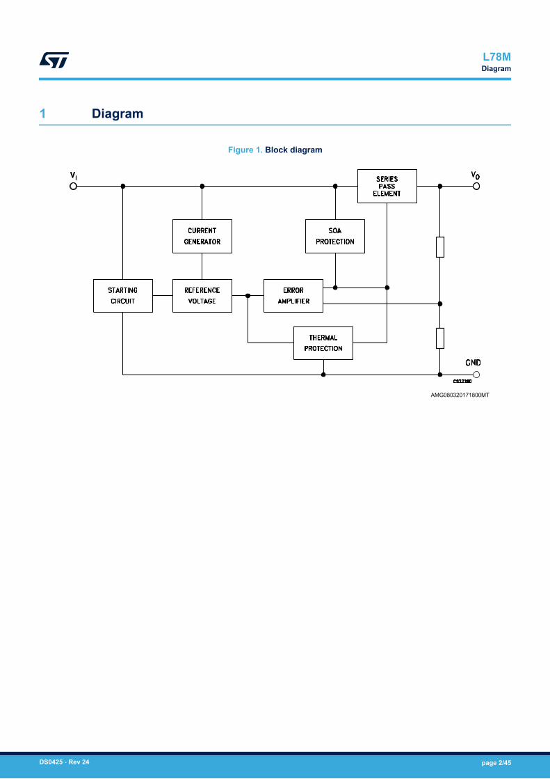
1 Diagram
Figure 1. Block diagram
AMG080320171800MT
L78MDiagram
DS0425 - Rev 24 page 2/45
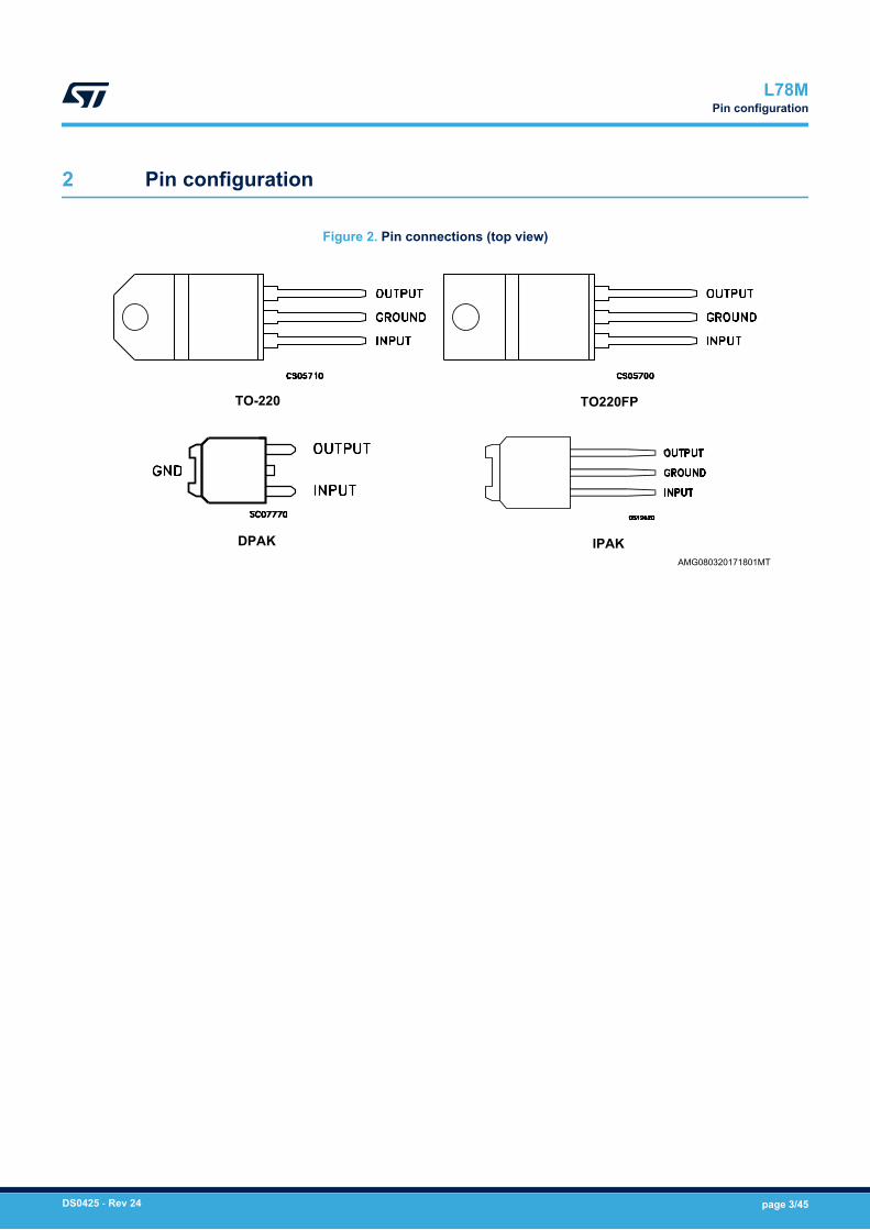
2 Pin configuration
Figure 2. Pin connections (top view)
AMG080320171801MT
L78MPin configuration
DS0425 - Rev 24 page 3/45
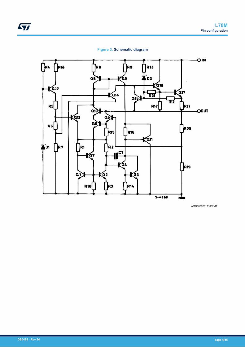
Figure 3. Schematic diagram
AMG080320171802MT
L78MPin configuration
DS0425 - Rev 24 page 4/45
3 Maximum ratings
Table 1. Absolute maximum ratings
Symbol Parameter Value Unit
VI DC input voltagefor VO = 5 to 18 V 35
Vfor VO = 20, 24 V 40
IO Output current Internally limited mA
PD Power dissipation Internally limited mW
TSTG Storage temperature range - 65 to 150 °C
TOP Operating junction temperature range
for L78MxxAC 0 to 125
°Cfor L78MxxAB -40 to 125
for L78MxxC 0 to 150
Note: Absolute maximum ratings are those values beyond which damage to the device may occur. Functionaloperation under these condition is not implied.
Table 2. Thermal data
Symbol Parameter TO-220 TO-220FP DPAK IPAK Unit
RthJC Thermal resistance junction-case 5 5 8 8 °C/W
RthJA Thermal resistance junction-ambient 50 60 100 100 °C/W
Figure 4. Application circuit
AMG080320171803MT
L78MMaximum ratings
DS0425 - Rev 24 page 5/45
4 Test circuits
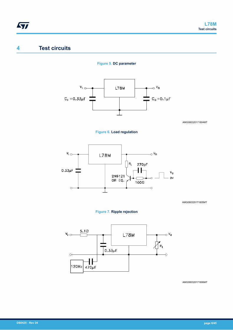
Figure 5. DC parameter
AMG080320171804MT
Figure 6. Load regulation
AMG080320171805MT
Figure 7. Ripple rejection
AMG080320171806MT
L78MTest circuits
DS0425 - Rev 24 page 6/45
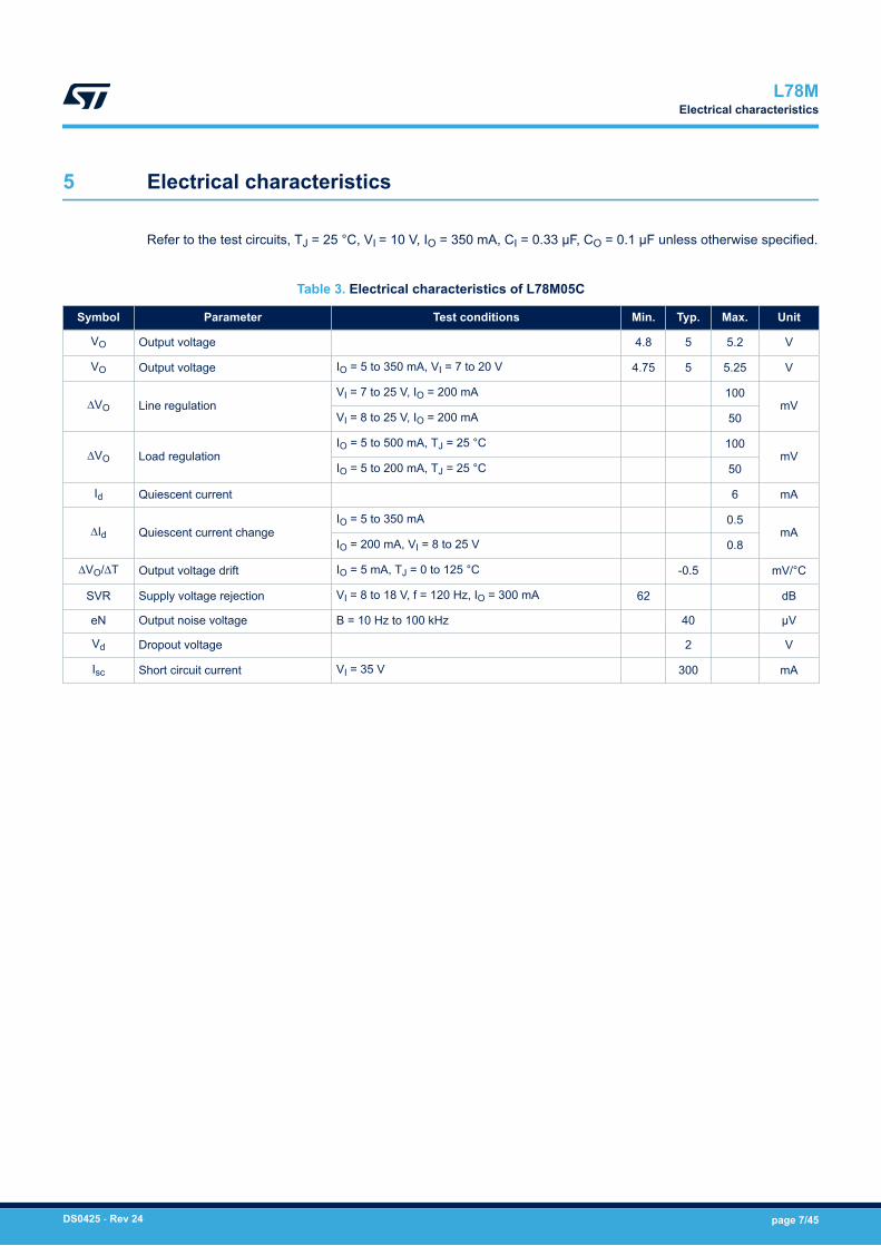
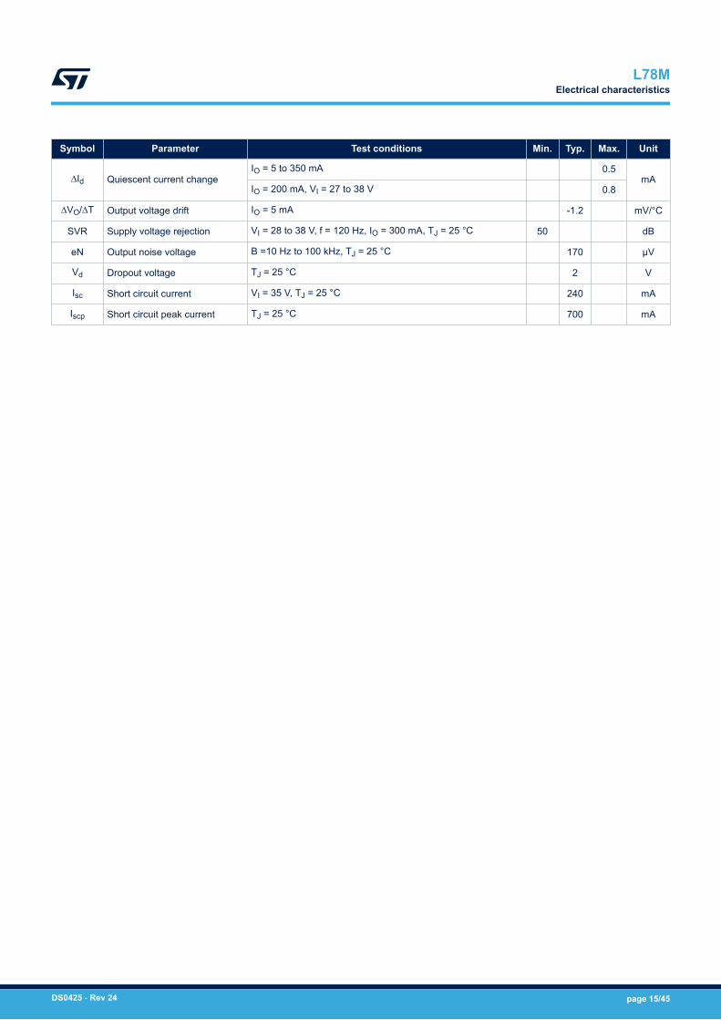
5 Electrical characteristics
Refer to the test circuits, TJ = 25 °C, VI = 10 V, IO = 350 mA, CI = 0.33 µF, CO = 0.1 µF unless otherwise specified.
Table 3. Electrical characteristics of L78M05C
Symbol Parameter Test conditions Min. Typ. Max. Unit
VO Output voltage 4.8 5 5.2 V
VO Output voltage IO = 5 to 350 mA, VI = 7 to 20 V 4.75 5 5.25 V
∆VO Line regulationVI = 7 to 25 V, IO = 200 mA 100
mVVI = 8 to 25 V, IO = 200 mA 50
∆VO Load regulationIO = 5 to 500 mA, TJ = 25 °C 100
mVIO = 5 to 200 mA, TJ = 25 °C 50
Id Quiescent current 6 mA
∆Id Quiescent current changeIO = 5 to 350 mA 0.5
mAIO = 200 mA, VI = 8 to 25 V 0.8
∆VO/∆T Output voltage drift IO = 5 mA, TJ = 0 to 125 °C -0.5 mV/°C
SVR Supply voltage rejection VI = 8 to 18 V, f = 120 Hz, IO = 300 mA 62 dB
eN Output noise voltage B = 10 Hz to 100 kHz 40 µV
Vd Dropout voltage 2 V
Isc Short circuit current VI = 35 V 300 mA
L78MElectrical characteristics
DS0425 - Rev 24 page 7/45
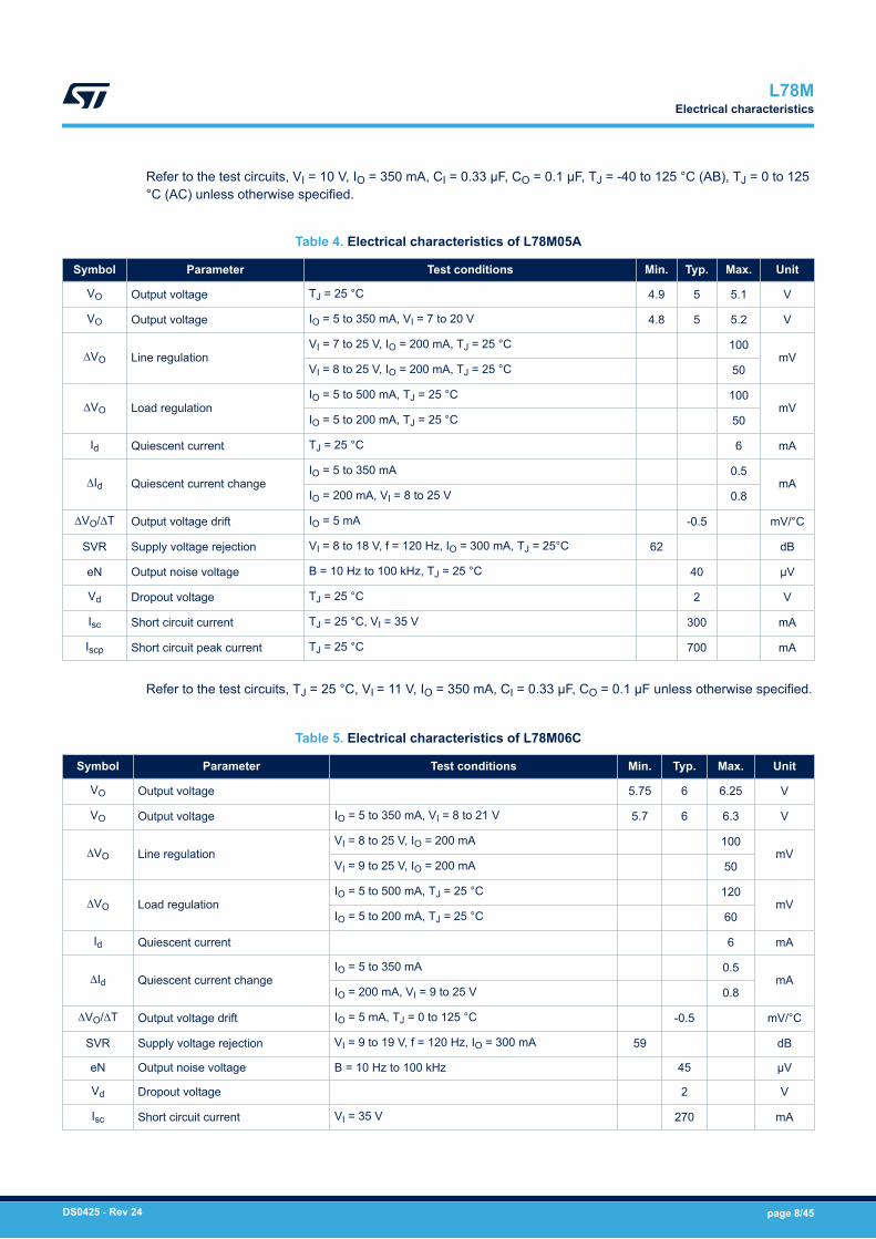
Refer to the test circuits, VI = 10 V, IO = 350 mA, CI = 0.33 µF, CO = 0.1 µF, TJ = -40 to 125 °C (AB), TJ = 0 to 125°C (AC) unless otherwise specified.
Table 4. Electrical characteristics of L78M05A
Symbol Parameter Test conditions Min. Typ. Max. Unit
VO Output voltage TJ = 25 °C 4.9 5 5.1 V
VO Output voltage IO = 5 to 350 mA, VI = 7 to 20 V 4.8 5 5.2 V
∆VO Line regulationVI = 7 to 25 V, IO = 200 mA, TJ = 25 °C 100
mVVI = 8 to 25 V, IO = 200 mA, TJ = 25 °C 50
∆VO Load regulationIO = 5 to 500 mA, TJ = 25 °C 100
mVIO = 5 to 200 mA, TJ = 25 °C 50
Id Quiescent current TJ = 25 °C 6 mA
∆Id Quiescent current changeIO = 5 to 350 mA 0.5
mAIO = 200 mA, VI = 8 to 25 V 0.8
∆VO/∆T Output voltage drift IO = 5 mA -0.5 mV/°C
SVR Supply voltage rejection VI = 8 to 18 V, f = 120 Hz, IO = 300 mA, TJ = 25°C 62 dB
eN Output noise voltage B = 10 Hz to 100 kHz, TJ = 25 °C 40 µV
Vd Dropout voltage TJ = 25 °C 2 V
Isc Short circuit current TJ = 25 °C, VI = 35 V 300 mA
Iscp Short circuit peak current TJ = 25 °C 700 mA
Refer to the test circuits, TJ = 25 °C, VI = 11 V, IO = 350 mA, CI = 0.33 µF, CO = 0.1 µF unless otherwise specified.
Table 5. Electrical characteristics of L78M06C
Symbol Parameter Test conditions Min. Typ. Max. Unit
VO Output voltage 5.75 6 6.25 V
VO Output voltage IO = 5 to 350 mA, VI = 8 to 21 V 5.7 6 6.3 V
∆VO Line regulationVI = 8 to 25 V, IO = 200 mA 100
mVVI = 9 to 25 V, IO = 200 mA 50
∆VO Load regulationIO = 5 to 500 mA, TJ = 25 °C 120
mVIO = 5 to 200 mA, TJ = 25 °C 60
Id Quiescent current 6 mA
∆Id Quiescent current changeIO = 5 to 350 mA 0.5
mAIO = 200 mA, VI = 9 to 25 V 0.8
∆VO/∆T Output voltage drift IO = 5 mA, TJ = 0 to 125 °C -0.5 mV/°C
SVR Supply voltage rejection VI = 9 to 19 V, f = 120 Hz, IO = 300 mA 59 dB
eN Output noise voltage B = 10 Hz to 100 kHz 45 µV
Vd Dropout voltage 2 V
Isc Short circuit current VI = 35 V 270 mA
L78MElectrical characteristics
DS0425 - Rev 24 page 8/45
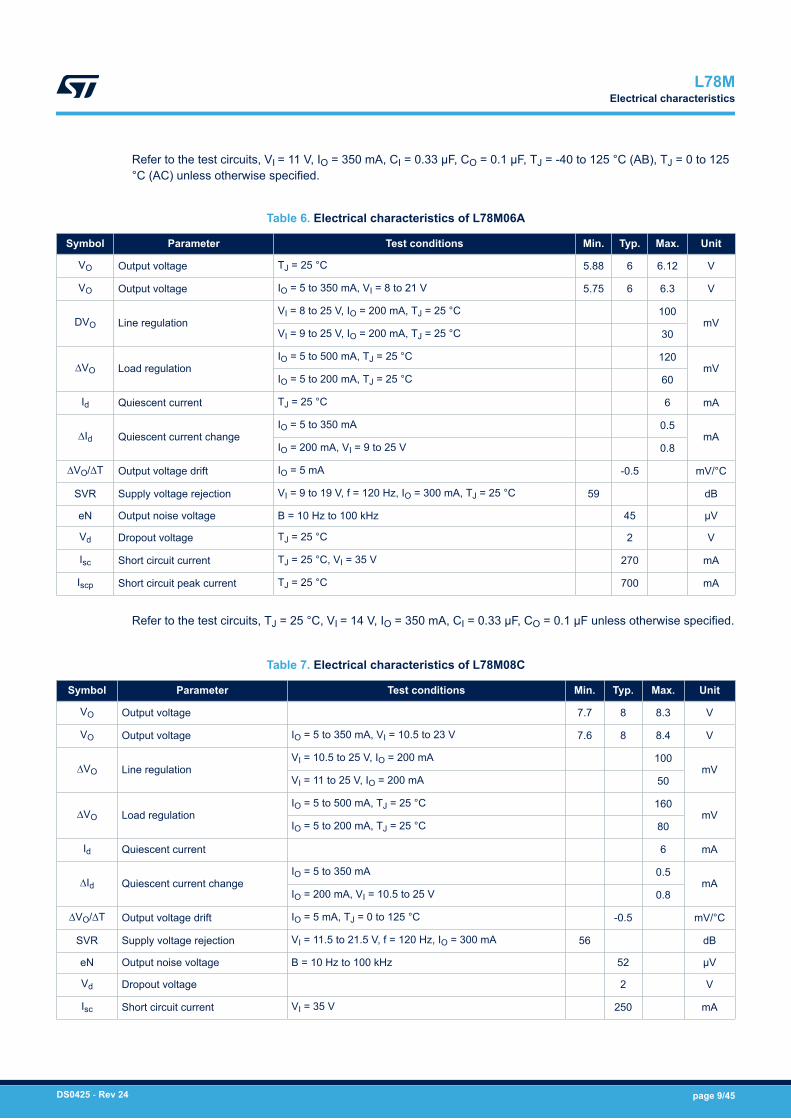
Refer to the test circuits, VI = 11 V, IO = 350 mA, CI = 0.33 µF, CO = 0.1 µF, TJ = -40 to 125 °C (AB), TJ = 0 to 125°C (AC) unless otherwise specified.
Table 6. Electrical characteristics of L78M06A
Symbol Parameter Test conditions Min. Typ. Max. Unit
VO Output voltage TJ = 25 °C 5.88 6 6.12 V
VO Output voltage IO = 5 to 350 mA, VI = 8 to 21 V 5.75 6 6.3 V
DVO Line regulationVI = 8 to 25 V, IO = 200 mA, TJ = 25 °C 100
mVVI = 9 to 25 V, IO = 200 mA, TJ = 25 °C 30
∆VO Load regulationIO = 5 to 500 mA, TJ = 25 °C 120
mVIO = 5 to 200 mA, TJ = 25 °C 60
Id Quiescent current TJ = 25 °C 6 mA
∆Id Quiescent current changeIO = 5 to 350 mA 0.5
mAIO = 200 mA, VI = 9 to 25 V 0.8
∆VO/∆T Output voltage drift IO = 5 mA -0.5 mV/°C
SVR Supply voltage rejection VI = 9 to 19 V, f = 120 Hz, IO = 300 mA, TJ = 25 °C 59 dB
eN Output noise voltage B = 10 Hz to 100 kHz 45 µV
Vd Dropout voltage TJ = 25 °C 2 V
Isc Short circuit current TJ = 25 °C, VI = 35 V 270 mA
Iscp Short circuit peak current TJ = 25 °C 700 mA
Refer to the test circuits, TJ = 25 °C, VI = 14 V, IO = 350 mA, CI = 0.33 µF, CO = 0.1 µF unless otherwise specified.
Table 7. Electrical characteristics of L78M08C
Symbol Parameter Test conditions Min. Typ. Max. Unit
VO Output voltage 7.7 8 8.3 V
VO Output voltage IO = 5 to 350 mA, VI = 10.5 to 23 V 7.6 8 8.4 V
∆VO Line regulationVI = 10.5 to 25 V, IO = 200 mA 100
mVVI = 11 to 25 V, IO = 200 mA 50
∆VO Load regulationIO = 5 to 500 mA, TJ = 25 °C 160
mVIO = 5 to 200 mA, TJ = 25 °C 80
Id Quiescent current 6 mA
∆Id Quiescent current changeIO = 5 to 350 mA 0.5
mAIO = 200 mA, VI = 10.5 to 25 V 0.8
∆VO/∆T Output voltage drift IO = 5 mA, TJ = 0 to 125 °C -0.5 mV/°C
SVR Supply voltage rejection VI = 11.5 to 21.5 V, f = 120 Hz, IO = 300 mA 56 dB
eN Output noise voltage B = 10 Hz to 100 kHz 52 µV
Vd Dropout voltage 2 V
Isc Short circuit current VI = 35 V 250 mA
L78MElectrical characteristics
DS0425 - Rev 24 page 9/45
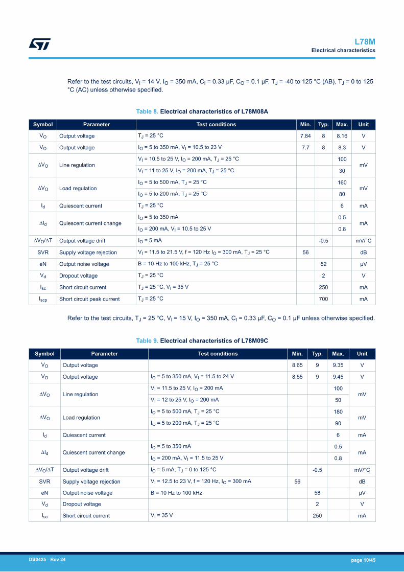
Refer to the test circuits, VI = 14 V, IO = 350 mA, CI = 0.33 µF, CO = 0.1 µF, TJ = -40 to 125 °C (AB), TJ = 0 to 125°C (AC) unless otherwise specified.
Table 8. Electrical characteristics of L78M08A
Symbol Parameter Test conditions Min. Typ. Max. Unit
VO Output voltage TJ = 25 °C 7.84 8 8.16 V
VO Output voltage IO = 5 to 350 mA, VI = 10.5 to 23 V 7.7 8 8.3 V
∆VO Line regulationVI = 10.5 to 25 V, IO = 200 mA, TJ = 25 °C 100
mVVI = 11 to 25 V, IO = 200 mA, TJ = 25 °C 30
∆VO Load regulationIO = 5 to 500 mA, TJ = 25 °C 160
mVIO = 5 to 200 mA, TJ = 25 °C 80
Id Quiescent current TJ = 25 °C 6 mA
∆Id Quiescent current changeIO = 5 to 350 mA 0.5
mAIO = 200 mA, VI = 10.5 to 25 V 0.8
∆VO/∆T Output voltage drift IO = 5 mA -0.5 mV/°C
SVR Supply voltage rejection VI = 11.5 to 21.5 V, f = 120 Hz IO = 300 mA, TJ = 25 °C 56 dB
eN Output noise voltage B = 10 Hz to 100 kHz, TJ = 25 °C 52 µV
Vd Dropout voltage TJ = 25 °C 2 V
Isc Short circuit current TJ = 25 °C, VI = 35 V 250 mA
Iscp Short circuit peak current TJ = 25 °C 700 mA
Refer to the test circuits, TJ = 25 °C, VI = 15 V, IO = 350 mA, CI = 0.33 µF, CO = 0.1 µF unless otherwise specified.
Table 9. Electrical characteristics of L78M09C
Symbol Parameter Test conditions Min. Typ. Max. Unit
VO Output voltage 8.65 9 9.35 V
VO Output voltage IO = 5 to 350 mA, VI = 11.5 to 24 V 8.55 9 9.45 V
∆VO Line regulationVI = 11.5 to 25 V, IO = 200 mA 100
mVVI = 12 to 25 V, IO = 200 mA 50
∆VO Load regulationIO = 5 to 500 mA, TJ = 25 °C 180
mVIO = 5 to 200 mA, TJ = 25 °C 90
Id Quiescent current 6 mA
∆Id Quiescent current changeIO = 5 to 350 mA 0.5
mAIO = 200 mA, VI = 11.5 to 25 V 0.8
∆VO/∆T Output voltage drift IO = 5 mA, TJ = 0 to 125 °C -0.5 mV/°C
SVR Supply voltage rejection VI = 12.5 to 23 V, f = 120 Hz, IO = 300 mA 56 dB
eN Output noise voltage B = 10 Hz to 100 kHz 58 µV
Vd Dropout voltage 2 V
Isc Short circuit current VI = 35 V 250 mA
L78MElectrical characteristics
DS0425 - Rev 24 page 10/45
Refer to the test circuits, VI = 15 V, IO = 350 mA, CI = 0.33 µF, CO = 0.1 µF, TJ = -40 to 125 °C (AB), TJ = 0 to 125°C (AC) unless otherwise specified.
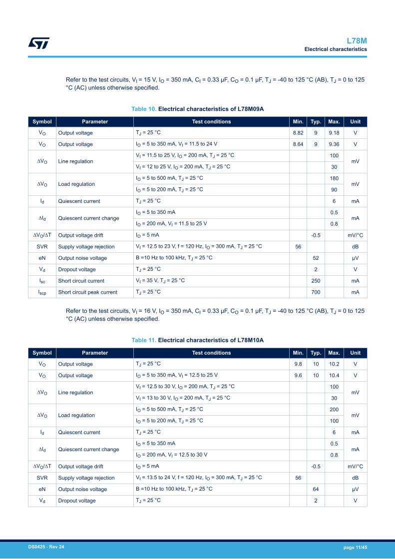
Table 10. Electrical characteristics of L78M09A
Symbol Parameter Test conditions Min. Typ. Max. Unit
VO Output voltage TJ = 25 °C 8.82 9 9.18 V
VO Output voltage IO = 5 to 350 mA, VI = 11.5 to 24 V 8.64 9 9.36 V
∆VO Line regulationVI = 11.5 to 25 V, IO = 200 mA, TJ = 25 °C 100
mVVI = 12 to 25 V, IO = 200 mA, TJ = 25 °C 30
∆VO Load regulationIO = 5 to 500 mA, TJ = 25 °C 180
mVIO = 5 to 200 mA, TJ = 25 °C 90
Id Quiescent current TJ = 25 °C 6 mA
∆Id Quiescent current changeIO = 5 to 350 mA 0.5
mAIO = 200 mA, VI = 11.5 to 25 V 0.8
∆VO/∆T Output voltage drift IO = 5 mA -0.5 mV/°C
SVR Supply voltage rejection VI = 12.5 to 23 V, f = 120 Hz, IO = 300 mA, TJ = 25 °C 56 dB
eN Output noise voltage B =10 Hz to 100 kHz, TJ = 25 °C 52 µV
Vd Dropout voltage TJ = 25 °C 2 V
Isc Short circuit current VI = 35 V, TJ = 25 °C 250 mA
Iscp Short circuit peak current TJ = 25 °C 700 mA
Refer to the test circuits, VI = 16 V, IO = 350 mA, CI = 0.33 µF, CO = 0.1 µF, TJ = -40 to 125 °C (AB), TJ = 0 to 125°C (AC) unless otherwise specified.
Table 11. Electrical characteristics of L78M10A
Symbol Parameter Test conditions Min. Typ. Max. Unit
VO Output voltage TJ = 25 °C 9.8 10 10.2 V
VO Output voltage IO = 5 to 350 mA, VI = 12.5 to 25 V 9.6 10 10.4 V
∆VO Line regulationVI = 12.5 to 30 V, IO = 200 mA, TJ = 25 °C 100
mVVI = 13 to 30 V, IO = 200 mA, TJ = 25 °C 30
∆VO Load regulationIO = 5 to 500 mA, TJ = 25 °C 200
mVIO = 5 to 200 mA, TJ = 25 °C 100
Id Quiescent current TJ = 25 °C 6 mA
∆Id Quiescent current changeIO = 5 to 350 mA 0.5
mAIO = 200 mA, VI = 12.5 to 30 V 0.8
∆VO/∆T Output voltage drift IO = 5 mA -0.5 mV/°C
SVR Supply voltage rejection VI = 13.5 to 24 V, f = 120 Hz, IO = 300 mA, TJ = 25 °C 56 dB
eN Output noise voltage B =10 Hz to 100 kHz, TJ = 25 °C 64 µV
Vd Dropout voltage TJ = 25 °C 2 V
L78MElectrical characteristics
DS0425 - Rev 24 page 11/45
Symbol Parameter Test conditions Min. Typ. Max. Unit
Isc Short circuit current VI = 35 V, TJ = 25 °C 245 mA
Iscp Short circuit peak current TJ = 25 °C 700 mA
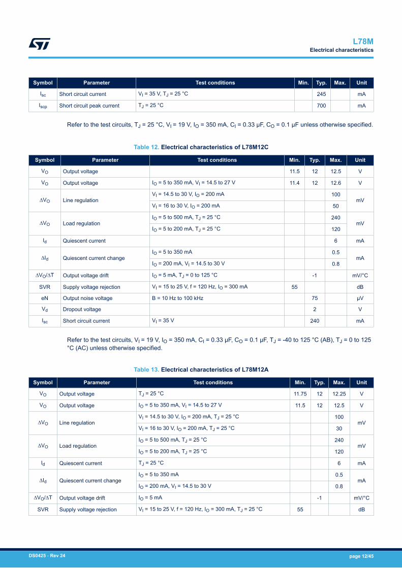
Refer to the test circuits, TJ = 25 °C, VI = 19 V, IO = 350 mA, CI = 0.33 µF, CO = 0.1 µF unless otherwise specified.
Table 12. Electrical characteristics of L78M12C
Symbol Parameter Test conditions Min. Typ. Max. Unit
VO Output voltage 11.5 12 12.5 V
VO Output voltage IO = 5 to 350 mA, VI = 14.5 to 27 V 11.4 12 12.6 V
∆VO Line regulationVI = 14.5 to 30 V, IO = 200 mA 100
mVVI = 16 to 30 V, IO = 200 mA 50
∆VO Load regulationIO = 5 to 500 mA, TJ = 25 °C 240
mVIO = 5 to 200 mA, TJ = 25 °C 120
Id Quiescent current 6 mA
∆Id Quiescent current changeIO = 5 to 350 mA 0.5
mAIO = 200 mA, VI = 14.5 to 30 V 0.8
∆VO/∆T Output voltage drift IO = 5 mA, TJ = 0 to 125 °C -1 mV/°C
SVR Supply voltage rejection VI = 15 to 25 V, f = 120 Hz, IO = 300 mA 55 dB
eN Output noise voltage B = 10 Hz to 100 kHz 75 µV
Vd Dropout voltage 2 V
Isc Short circuit current VI = 35 V 240 mA
Refer to the test circuits, VI = 19 V, IO = 350 mA, CI = 0.33 µF, CO = 0.1 µF, TJ = -40 to 125 °C (AB), TJ = 0 to 125°C (AC) unless otherwise specified.
Table 13. Electrical characteristics of L78M12A
Symbol Parameter Test conditions Min. Typ. Max. Unit
VO Output voltage TJ = 25 °C 11.75 12 12.25 V
VO Output voltage IO = 5 to 350 mA, VI = 14.5 to 27 V 11.5 12 12.5 V
∆VO Line regulationVI = 14.5 to 30 V, IO = 200 mA, TJ = 25 °C 100
mVVI = 16 to 30 V, IO = 200 mA, TJ = 25 °C 30
∆VO Load regulationIO = 5 to 500 mA, TJ = 25 °C 240
mVIO = 5 to 200 mA, TJ = 25 °C 120
Id Quiescent current TJ = 25 °C 6 mA
∆Id Quiescent current changeIO = 5 to 350 mA 0.5
mAIO = 200 mA, VI = 14.5 to 30 V 0.8
∆VO/∆T Output voltage drift IO = 5 mA -1 mV/°C
SVR Supply voltage rejection VI = 15 to 25 V, f = 120 Hz, IO = 300 mA, TJ = 25 °C 55 dB
L78MElectrical characteristics
DS0425 - Rev 24 page 12/45
Symbol Parameter Test conditions Min. Typ. Max. Unit
eN Output noise voltage B = 10 Hz to 100 kHz, TJ = 25 °C 75 µV
Vd Dropout voltage TJ = 25 °C 2 V
Isc Short circuit current VI = 35 V, TJ = 25 °C 240 mA
Iscp Short circuit peak current TJ = 25 °C 700 mA
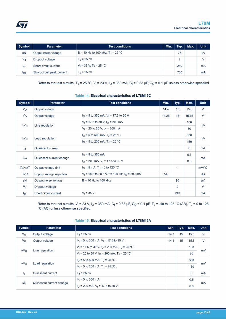
Refer to the test circuits, TJ = 25 °C, VI = 23 V, IO = 350 mA, CI = 0.33 µF, CO = 0.1 µF unless otherwise specified.
Table 14. Electrical characteristics of L78M15C
Symbol Parameter Test conditions Min. Typ. Max. Unit
VO Output voltage 14.4 15 15.6 V
VO Output voltage IO = 5 to 350 mA, VI = 17.5 to 30 V 14.25 15 15.75 V
∆VO Line regulationVI = 17.5 to 30 V, IO = 200 mA 100
mVVI = 20 to 30 V, IO = 200 mA 50
∆VO Load regulationIO = 5 to 500 mA, TJ = 25 °C 300
mVIO = 5 to 200 mA, TJ = 25 °C 150
Id Quiescent current 6 mA
∆Id Quiescent current changeIO = 5 to 350 mA 0.5
mAIO = 200 mA, VI = 17.5 to 30 V 0.8
∆VO/∆T Output voltage drift IO = 5 mA, TJ = 0 to 125 °C -1 mV/°C
SVR Supply voltage rejection VI = 18.5 to 28.5 V, f = 120 Hz, IO = 300 mA 54 dB
eN Output noise voltage B = 10 Hz to 100 kHz 90 µV
Vd Dropout voltage 2 V
Isc Short circuit current VI = 35 V 240 mA
Refer to the test circuits, VI = 23 V, IO = 350 mA, CI = 0.33 µF, CO = 0.1 µF, TJ = -40 to 125 °C (AB), TJ = 0 to 125°C (AC) unless otherwise specified.
Table 15. Electrical characteristics of L78M15A
Symbol Parameter Test conditions Min. Typ. Max. Unit
VO Output voltage TJ = 25 °C 14.7 15 15.3 V
VO Output voltage IO = 5 to 350 mA, VI = 17.5 to 30 V 14.4 15 15.6 V
∆VO Line regulationVI = 17.5 to 30 V, IO = 200 mA, TJ = 25 °C 100
mVVI = 20 to 30 V, IO = 200 mA, TJ = 25 °C 30
∆VO Load regulationIO = 5 to 500 mA, TJ = 25 °C 300
mVIO = 5 to 200 mA, TJ = 25 °C 150
Id Quiescent current TJ = 25 °C 6 mA
∆Id Quiescent current changeIO = 5 to 350 mA 0.5
mAIO = 200 mA, VI = 17.5 to 30 V 0.8
L78MElectrical characteristics
DS0425 - Rev 24 page 13/45
Symbol Parameter Test conditions Min. Typ. Max. Unit
∆VO/∆T Output voltage drift IO = 5 mA -1 mV/°C
SVR Supply voltage rejection VI = 18.5 to 28.5 V, f = 120 Hz, IO = 300 mA, TJ = 25 °C 54 dB
eN Output noise voltage B =10 Hz to 100 kHz, TJ = 25 °C 90 µV
Vd Dropout voltage TJ = 25 °C 2 V
Isc Short circuit current VI = 35 V, TJ = 25 °C 240 mA
Iscp Short circuit peak current TJ = 25 °C 700 mA
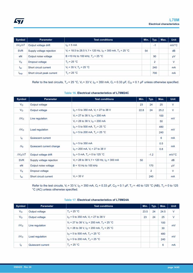
Refer to the test circuits, TJ = 25 °C, VI = 33 V, IO = 350 mA, CI = 0.33 µF, CO = 0.1 µF unless otherwise specified.
Table 16. Electrical characteristics of L78M24C
Symbol Parameter Test conditions Min. Typ. Max. Unit
VO Output voltage 23 24 25 V
VO Output voltage IO = 5 to 350 mA, VI = 27 to 38 V 22.8 24 25.2 V
∆VO Line regulationVI = 27 to 38 V, IO = 200 mA 100
mVVI = 28 to 38 V, IO = 200 mA 50
∆VO Load regulationIO = 5 to 500 mA, TJ = 25 °C 480
mVIO = 5 to 200 mA, TJ = 25 °C 240
Id Quiescent current 6 mA
∆Id Quiescent current changeIO = 5 to 350 mA 0.5
mAIO = 200 mA, VI = 27 to 38 V 0.8
∆VO/∆T Output voltage drift IO = 5 mA, TJ = 0 to 125 °C -1.2 mV/°C
SVR Supply voltage rejection VI = 28 to 38 V, f = 120 Hz, IO = 300 mA 50 dB
eN Output noise voltage B = 10 Hz to 100 kHz 170 µV
Vd Dropout voltage 2 V
Isc Short circuit current VI = 35 V 240 mA
Refer to the test circuits, VI = 33 V, IO = 350 mA, CI = 0.33 µF, CO = 0.1 µF, TJ = -40 to 125 °C (AB), TJ = 0 to 125°C (AC) unless otherwise specified.
Table 17. Electrical characteristics of L78M24A
Symbol Parameter Test conditions Min. Typ. Max. Unit
VO Output voltage TJ = 25 °C 23.5 24 24.5 V
VO Output voltage IO = 5 to 350 mA, VI = 27 to 38 V 23 24 25 V
∆VO Line regulationVI = 27 to 38 V, IO = 200 mA, TJ = 25 °C 100
mVVI = 28 to 38 V, IO = 200 mA, TJ = 25 °C 30
∆VO Load regulationIO = 5 to 500 mA, TJ = 25 °C 480
mVIO = 5 to 200 mA, TJ = 25 °C 240
Id Quiescent current TJ = 25 °C 6 mA
L78MElectrical characteristics
DS0425 - Rev 24 page 14/45
Symbol Parameter Test conditions Min. Typ. Max. Unit
∆Id Quiescent current changeIO = 5 to 350 mA 0.5
mAIO = 200 mA, VI = 27 to 38 V 0.8
∆VO/∆T Output voltage drift IO = 5 mA -1.2 mV/°C
SVR Supply voltage rejection VI = 28 to 38 V, f = 120 Hz, IO = 300 mA, TJ = 25 °C 50 dB
eN Output noise voltage B =10 Hz to 100 kHz, TJ = 25 °C 170 µV
Vd Dropout voltage TJ = 25 °C 2 V
Isc Short circuit current VI = 35 V, TJ = 25 °C 240 mA
Iscp Short circuit peak current TJ = 25 °C 700 mA
L78MElectrical characteristics
DS0425 - Rev 24 page 15/45
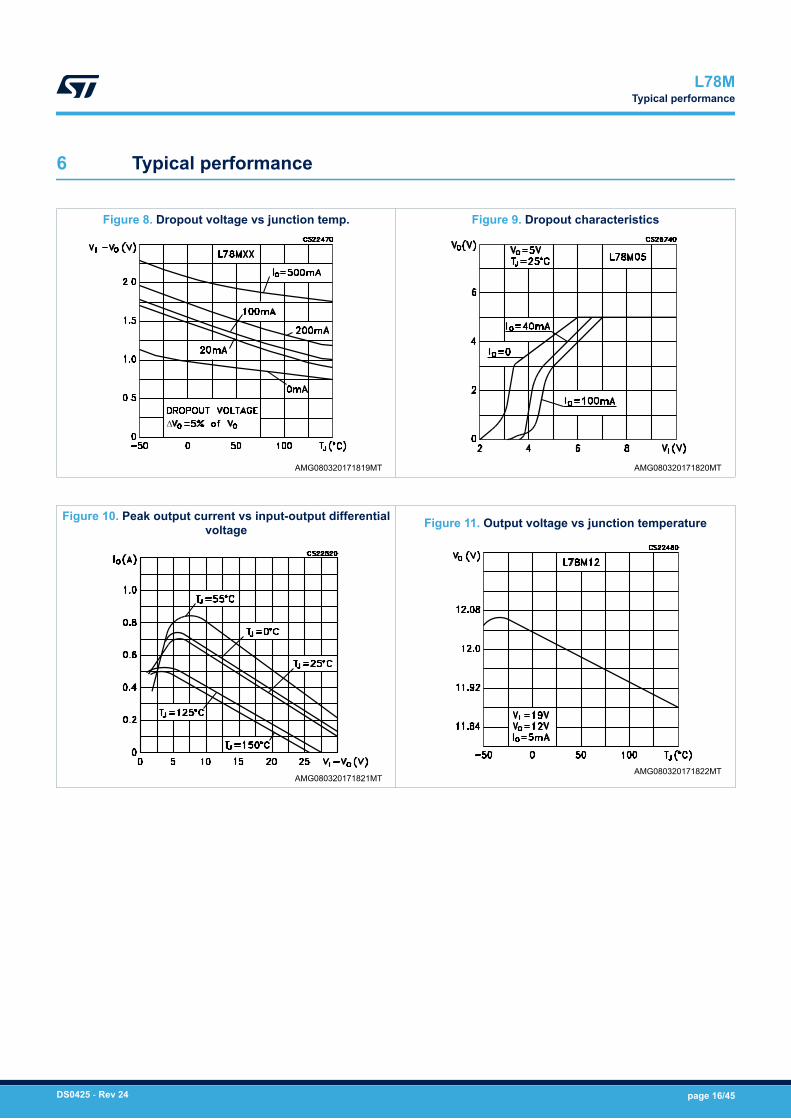
6 Typical performance
Figure 8. Dropout voltage vs junction temp.
AMG080320171819MT
Figure 9. Dropout characteristics
AMG080320171820MT
Figure 10. Peak output current vs input-output differentialvoltage
AMG080320171821MT
Figure 11. Output voltage vs junction temperature
AMG080320171822MT
L78MTypical performance
DS0425 - Rev 24 page 16/45
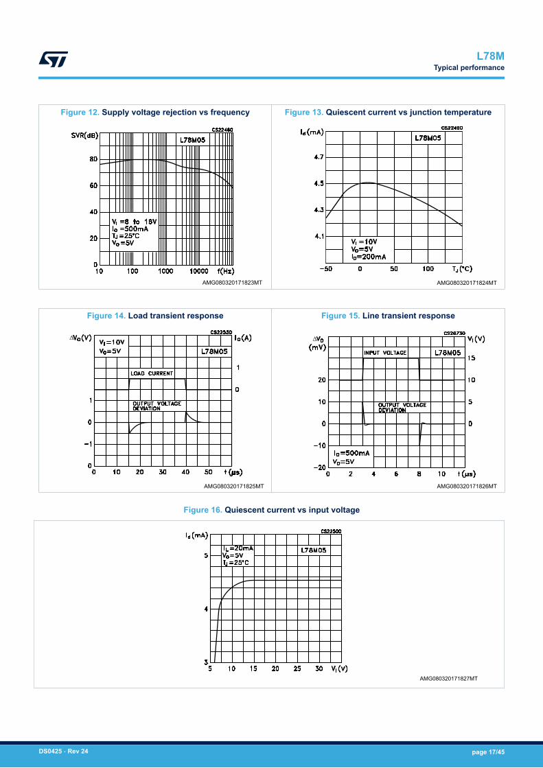
Figure 12. Supply voltage rejection vs frequency
AMG080320171823MT
Figure 13. Quiescent current vs junction temperature
AMG080320171824MT
Figure 14. Load transient response
AMG080320171825MT
Figure 15. Line transient response
AMG080320171826MT
Figure 16. Quiescent current vs input voltage
AMG080320171827MT
L78MTypical performance
DS0425 - Rev 24 page 17/45
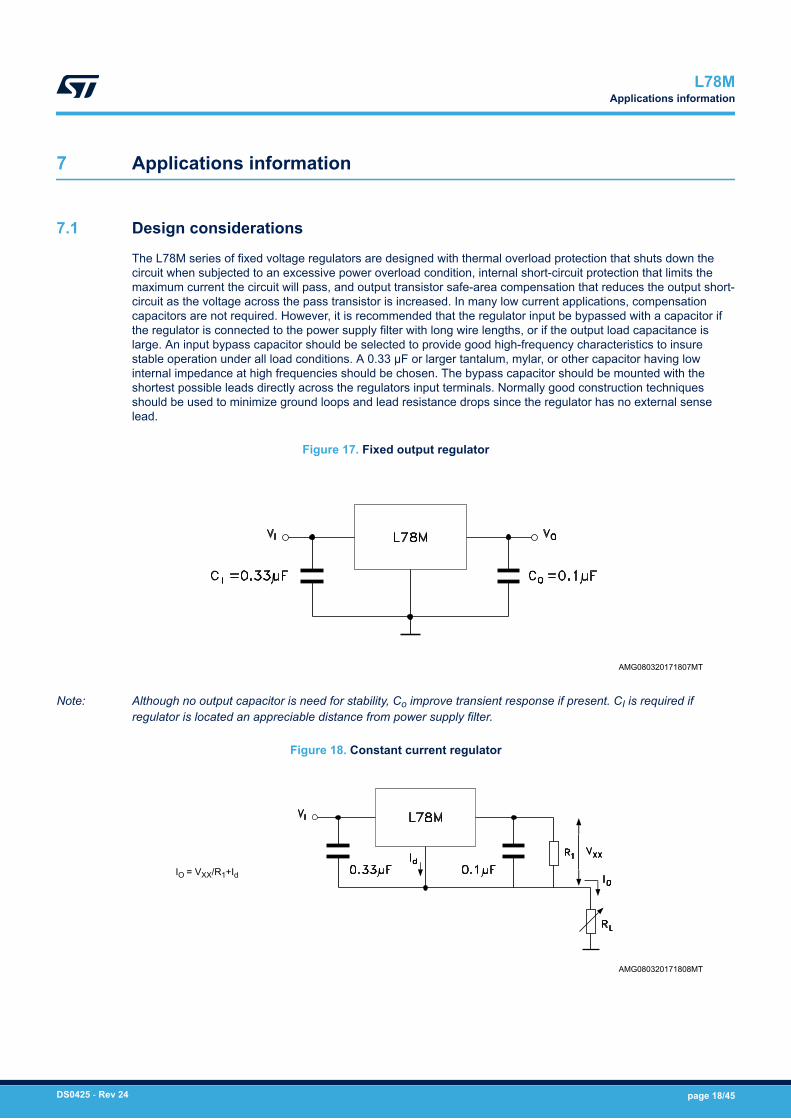
7 Applications information
7.1 Design considerations
The L78M series of fixed voltage regulators are designed with thermal overload protection that shuts down thecircuit when subjected to an excessive power overload condition, internal short-circuit protection that limits themaximum current the circuit will pass, and output transistor safe-area compensation that reduces the output short-circuit as the voltage across the pass transistor is increased. In many low current applications, compensationcapacitors are not required. However, it is recommended that the regulator input be bypassed with a capacitor ifthe regulator is connected to the power supply filter with long wire lengths, or if the output load capacitance islarge. An input bypass capacitor should be selected to provide good high-frequency characteristics to insurestable operation under all load conditions. A 0.33 µF or larger tantalum, mylar, or other capacitor having lowinternal impedance at high frequencies should be chosen. The bypass capacitor should be mounted with theshortest possible leads directly across the regulators input terminals. Normally good construction techniquesshould be used to minimize ground loops and lead resistance drops since the regulator has no external senselead.
Figure 17. Fixed output regulator
AMG080320171807MT
Note: Although no output capacitor is need for stability, Co improve transient response if present. CI is required ifregulator is located an appreciable distance from power supply filter.
Figure 18. Constant current regulator
AMG080320171808MT
IO = VXX/R1+Id
L78MApplications information
DS0425 - Rev 24 page 18/45
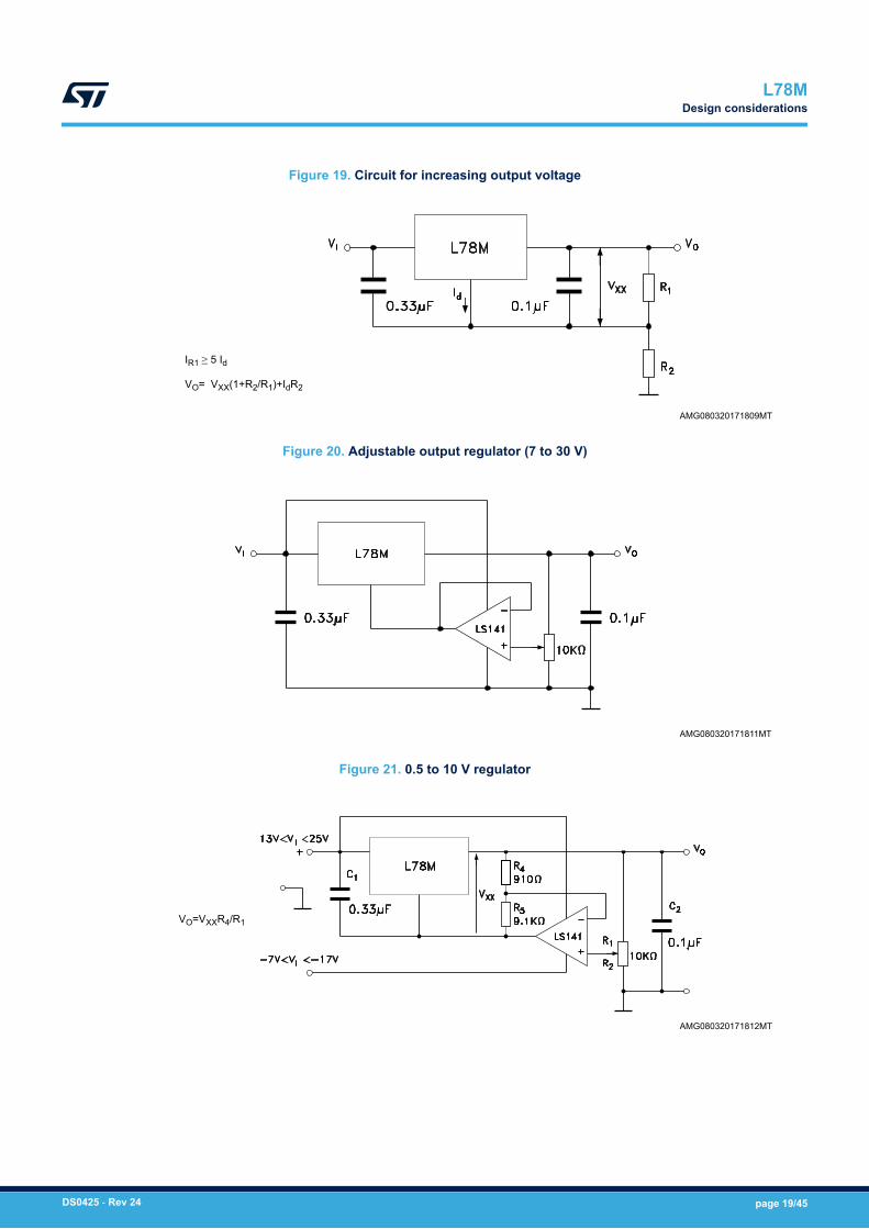
Figure 19. Circuit for increasing output voltage
AMG080320171809MT
IR1 ≥ 5 Id
VO= VXX(1+R2/R1)+IdR2
Figure 20. Adjustable output regulator (7 to 30 V)
AMG080320171811MT
Figure 21. 0.5 to 10 V regulator
VO=VXXR4/R1
AMG080320171812MT
L78MDesign considerations
DS0425 - Rev 24 page 19/45
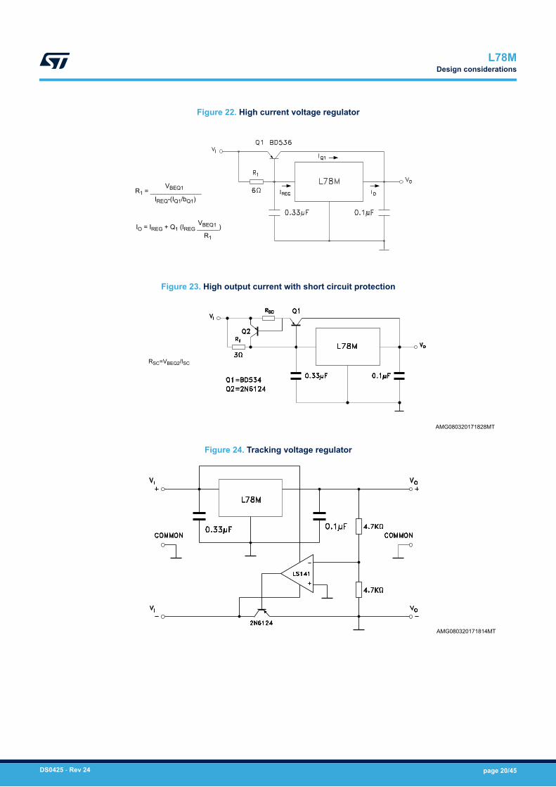
Figure 22. High current voltage regulator
R1
IO = IREG + Q1 (IREG _V____BEQ1_)
VBEQ1R1 = ______________IREQ-(IQ1/bQ1)
Figure 23. High output current with short circuit protection
RSC=VBEQ2/ISC
AMG080320171828MT
Figure 24. Tracking voltage regulator
AMG080320171814MT
L78MDesign considerations
DS0425 - Rev 24 page 20/45
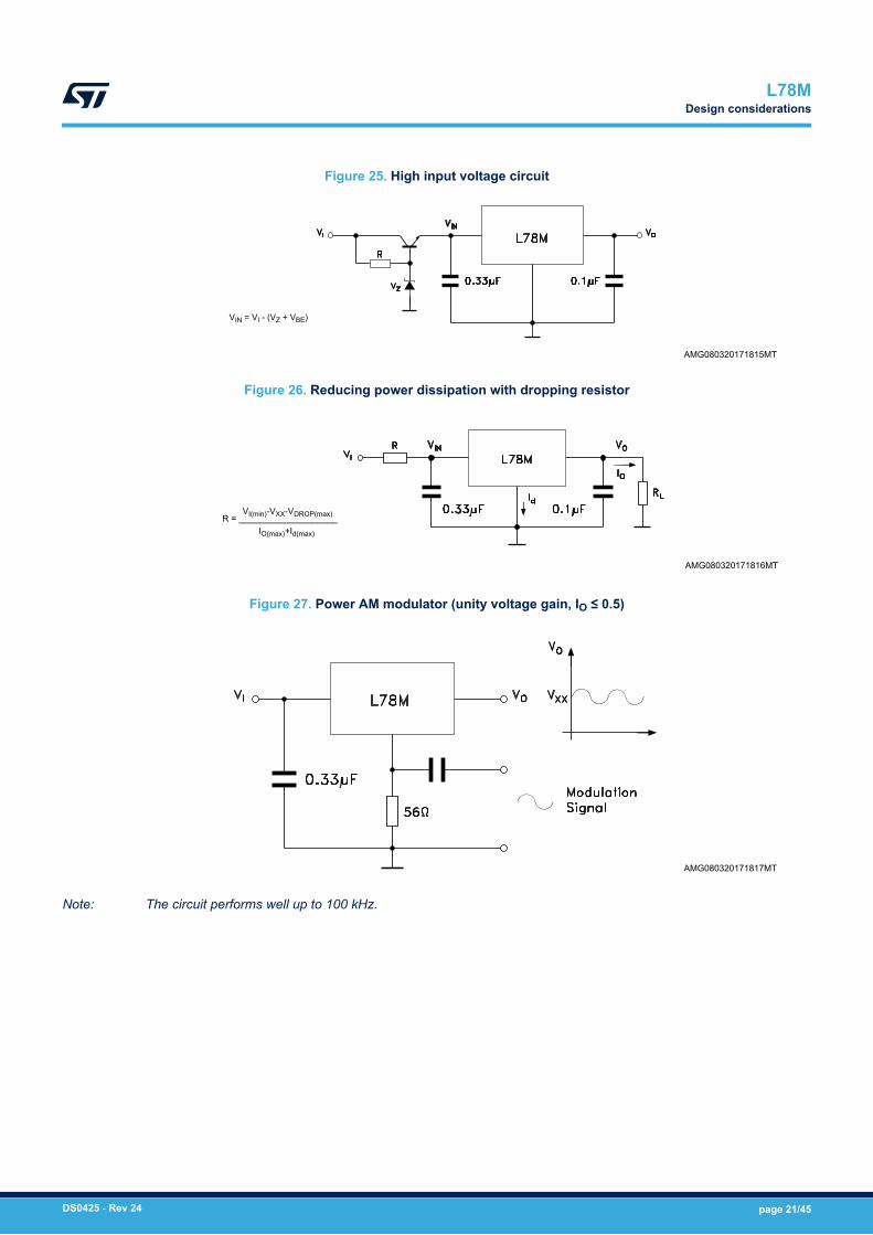
Figure 25. High input voltage circuit
VIN = VI - (VZ + VBE)
AMG080320171815MT
Figure 26. Reducing power dissipation with dropping resistor
V -V -VR = __I(mi___n)____XX___DRO____P(max)____
IO(max)+Id(max)
AMG080320171816MT
Figure 27. Power AM modulator (unity voltage gain, IO ≤ 0.5)
AMG080320171817MT
Note: The circuit performs well up to 100 kHz.
L78MDesign considerations
DS0425 - Rev 24 page 21/45
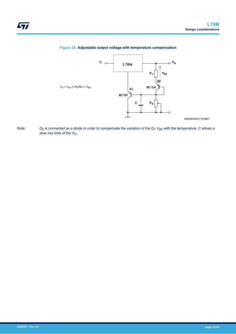
Figure 28. Adjustable output voltage with temperature compensation
VO = VXX (1+R2/R1) + VBE
AMG080320171818MT
Note: Q2 is connected as a diode in order to compensate the variation of the Q1 VBE with the temperature. C allows aslow rise time of the VO.
L78MDesign considerations
DS0425 - Rev 24 page 22/45
8 Package information
In order to meet environmental requirements, ST offers these devices in different grades of ECOPACK packages,depending on their level of environmental compliance. ECOPACK specifications, grade definitions and productstatus are available at: www.st.com. ECOPACK is an ST trademark.
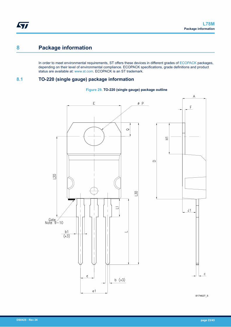
8.1 TO-220 (single gauge) package information
Figure 29. TO-220 (single gauge) package outline
8174627_5
L78MPackage information
DS0425 - Rev 24 page 23/45
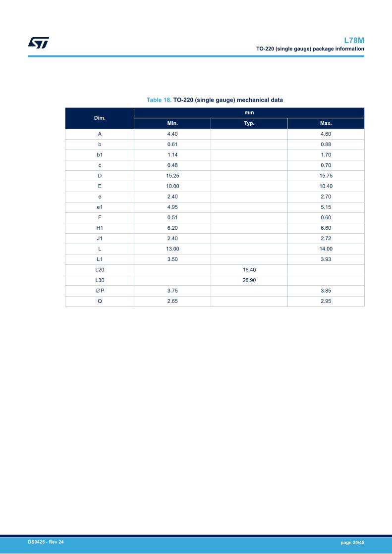
Table 18. TO-220 (single gauge) mechanical data
Dim.mm
Min. Typ. Max.
A 4.40 4.60
b 0.61 0.88
b1 1.14 1.70
c 0.48 0.70
D 15.25 15.75
E 10.00 10.40
e 2.40 2.70
e1 4.95 5.15
F 0.51 0.60
H1 6.20 6.60
J1 2.40 2.72
L 13.00 14.00
L1 3.50 3.93
L20 16.40
L30 28.90
∅P 3.75 3.85
Q 2.65 2.95
L78MTO-220 (single gauge) package information
DS0425 - Rev 24 page 24/45
8.2 TO-220 (dual gauge) package information
Figure 30. TO-220 (dual gauge) package outline
0015988_21_Type A
L78MTO-220 (dual gauge) package information
DS0425 - Rev 24 page 25/45

Table 19. TO-220 (dual gauge) mechanical data
Dim.mm
Min. Typ. Max.
A 4.40 4.60
b 0.61 0.88
b1 1.14 1.70
c 0.48 0.70
D 15.25 15.75
D1 1.27
E 10 10.40
e 2.40 2.70
e1 4.95 5.15
F 1.23 1.32
H1 6.20 6.60
J1 2.40 2.72
L 13 14
L1 3.50 3.93
L20 16.40
L30 28.90
∅P 3.75 3.85
Q 2.65 2.95
L78MTO-220 (dual gauge) package information
DS0425 - Rev 24 page 26/45
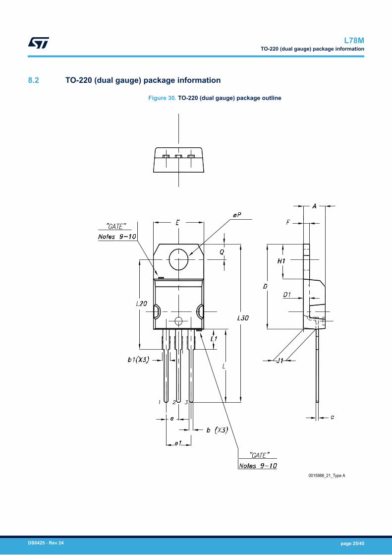
8.3 TO-220FP type A package information
Figure 31. TO-220FP package outline
7012510_type_A
L78MTO-220FP type A package information
DS0425 - Rev 24 page 27/45
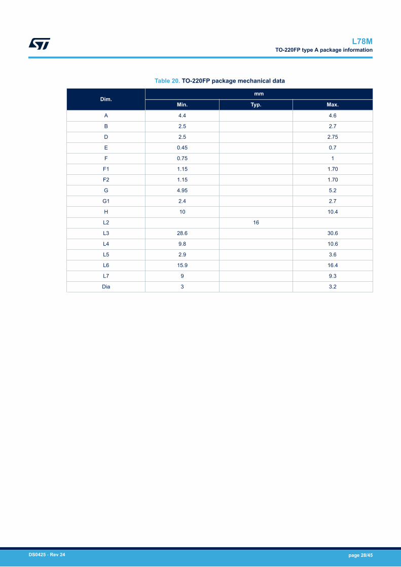
Table 20. TO-220FP package mechanical data
Dim.mm
Min. Typ. Max.
A 4.4 4.6
B 2.5 2.7
D 2.5 2.75
E 0.45 0.7
F 0.75 1
F1 1.15 1.70
F2 1.15 1.70
G 4.95 5.2
G1 2.4 2.7
H 10 10.4
L2 16
L3 28.6 30.6
L4 9.8 10.6
L5 2.9 3.6
L6 15.9 16.4
L7 9 9.3
Dia 3 3.2
L78MTO-220FP type A package information
DS0425 - Rev 24 page 28/45
8.4 DPAK (TO-252) package information
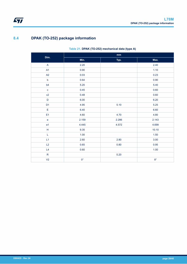
Table 21. DPAK (TO-252) mechanical data (type A)
Dim.mm
Min. Typ. Max.
A 2.20 2.40
A1 0.90 1.10
A2 0.03 0.23
b 0.64 0.90
b4 5.20 5.40
c 0.45 0.60
c2 0.48 0.60
D 6.00 6.20
D1 4.95 5.10 5.25
E 6.40 6.60
E1 4.60 4.70 4.80
e 2.159 2.286 2.143
e1 4.445 4.572 4.699
H 9.35 10.10
L 1.00 1.50
L1 2.60 2.80 3.00
L2 0.65 0.80 0.95
L4 0.60 1.00
R 0.20
V2 0° 8°
L78MDPAK (TO-252) package information
DS0425 - Rev 24 page 29/45
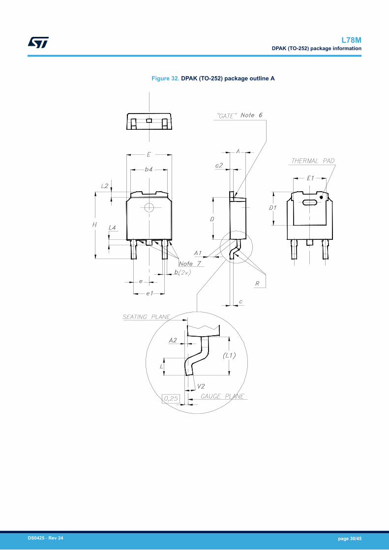
Figure 32. DPAK (TO-252) package outline A
L78MDPAK (TO-252) package information
DS0425 - Rev 24 page 30/45

Table 22. DPAK(TO-252) mechanical data (type E)
Dim.mm
Min. Typ. Max.
A 2.18 2.39
A2 0.13
b 0.65 0.884
b4 4.95 5.46
c 0.46 0.61
c2 0.46 0.60
D 5.97 6.22
D1 5.21
E 6.35 6.73
E1 4.32
e 2.286
e1 4.572
H 9.94 10.34
L 1.50 1.78
L1 2.74
L2 0.89 1.27
L4 1.02
L78MDPAK (TO-252) package information
DS0425 - Rev 24 page 31/45
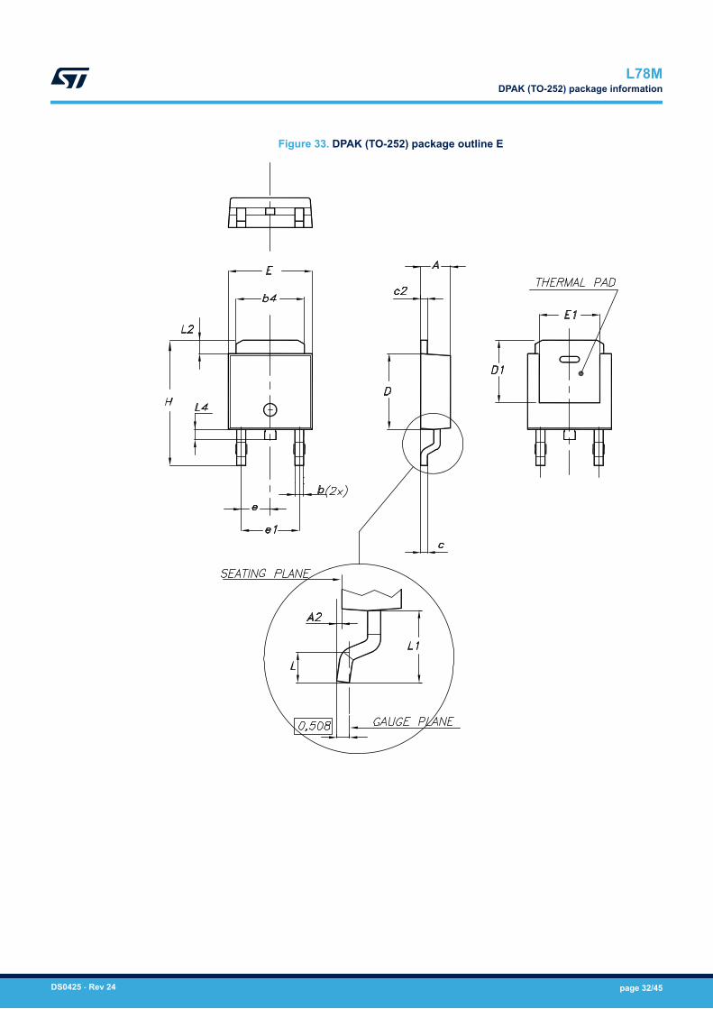
Figure 33. DPAK (TO-252) package outline E
L78MDPAK (TO-252) package information
DS0425 - Rev 24 page 32/45
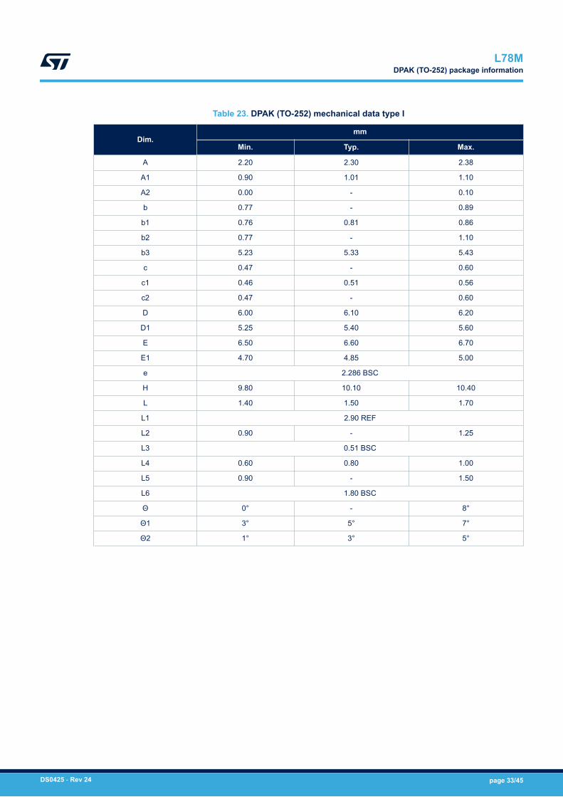
Table 23. DPAK (TO-252) mechanical data type I
Dim.mm
Min. Typ. Max.
A 2.20 2.30 2.38
A1 0.90 1.01 1.10
A2 0.00 - 0.10
b 0.77 - 0.89
b1 0.76 0.81 0.86
b2 0.77 - 1.10
b3 5.23 5.33 5.43
c 0.47 - 0.60
c1 0.46 0.51 0.56
c2 0.47 - 0.60
D 6.00 6.10 6.20
D1 5.25 5.40 5.60
E 6.50 6.60 6.70
E1 4.70 4.85 5.00
e 2.286 BSC
H 9.80 10.10 10.40
L 1.40 1.50 1.70
L1 2.90 REF
L2 0.90 - 1.25
L3 0.51 BSC
L4 0.60 0.80 1.00
L5 0.90 - 1.50
L6 1.80 BSC
Θ 0° - 8°
Θ1 3° 5° 7°
Θ2 1° 3° 5°
L78MDPAK (TO-252) package information
DS0425 - Rev 24 page 33/45
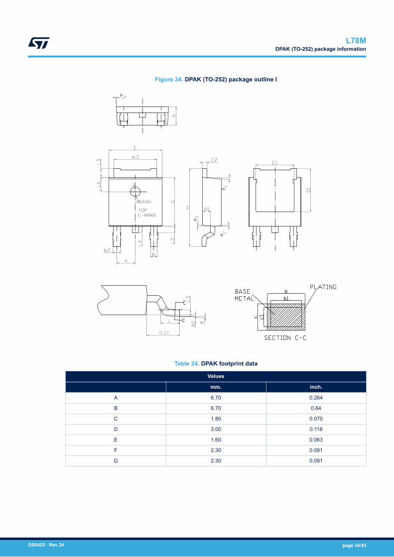
Figure 34. DPAK (TO-252) package outline I
Table 24. DPAK footprint data
Values
mm. inch.
A 6.70 0.264
B 6.70 0.64
C 1.80 0.070
D 3.00 0.118
E 1.60 0.063
F 2.30 0.091
G 2.30 0.091
L78MDPAK (TO-252) package information
DS0425 - Rev 24 page 34/45
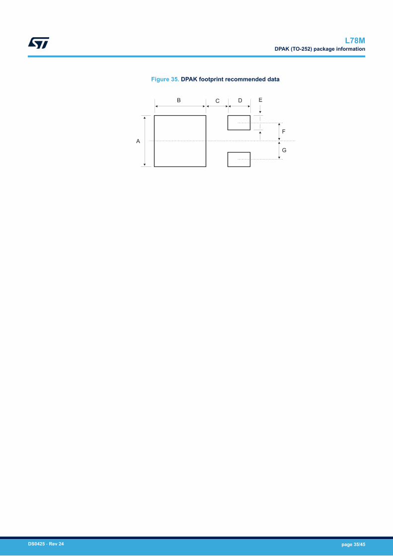
Figure 35. DPAK footprint recommended data
A
E
F
G
B C D
L78MDPAK (TO-252) package information
DS0425 - Rev 24 page 35/45
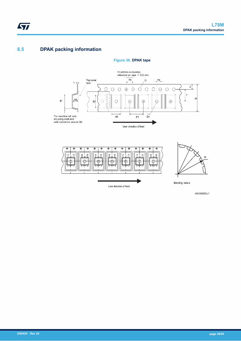
8.5 DPAK packing information
Figure 36. DPAK tape
L78MDPAK packing information
DS0425 - Rev 24 page 36/45
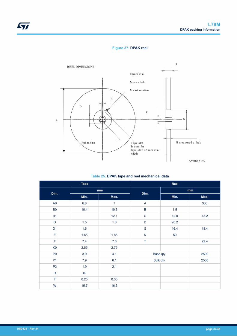
Figure 37. DPAK reel
A
D
B
Full radius G measured a t hub
C
N
REEL DIMENSIONS
40mm min.
Access hole
At s lot loca tion
T
Tape s lot in core fortape s ta rt 25 mm min.width
AM08851v2
Table 25. DPAK tape and reel mechanical data
Tape Reel
Dim.mm
Dim.mm
Min. Max. Min. Max.
A0 6.8 7 A 330
B0 10.4 10.6 B 1.5
B1 12.1 C 12.8 13.2
D 1.5 1.6 D 20.2
D1 1.5 G 16.4 18.4
E 1.65 1.85 N 50
F 7.4 7.6 T 22.4
K0 2.55 2.75
P0 3.9 4.1 Base qty. 2500
P1 7.9 8.1 Bulk qty. 2500
P2 1.9 2.1
R 40
T 0.25 0.35
W 15.7 16.3
L78MDPAK packing information
DS0425 - Rev 24 page 37/45
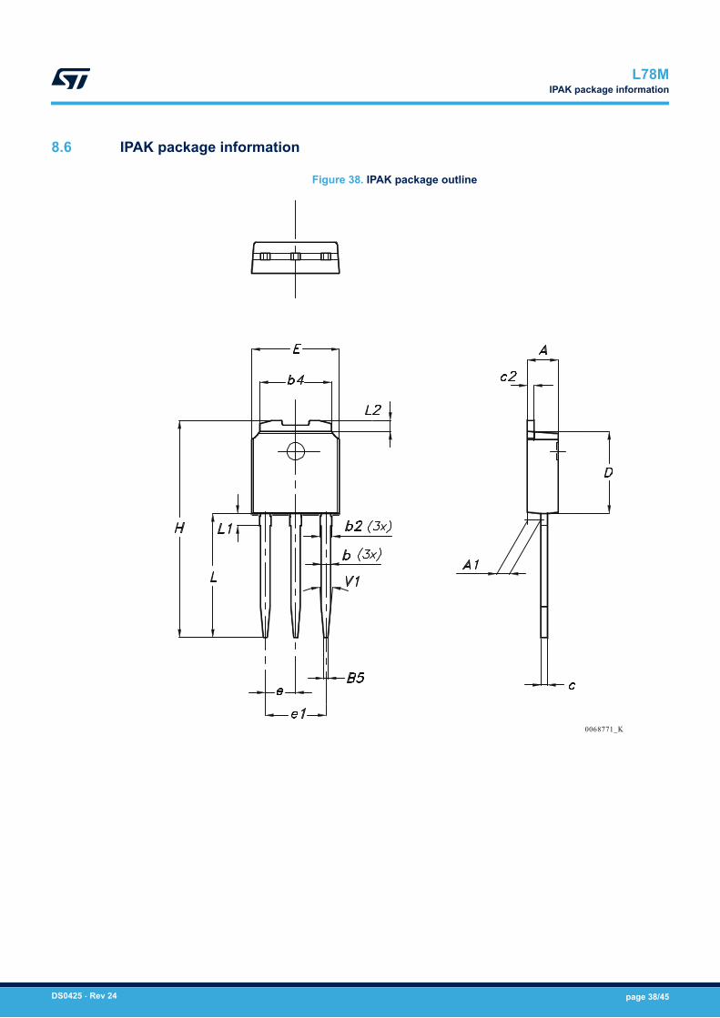
8.6 IPAK package information
Figure 38. IPAK package outline
0068771_K
L78MIPAK package information
DS0425 - Rev 24 page 38/45
Table 26. IPAK mechanical data
Dim.mm
Min. Typ. Max.
A 2.20 2.40
A1 0.90 1.10
b 0.64 0.90
b2 0.95
b4 5.20 5.40
B5 0.30
c 0.45 0.60
c2 0.48 0.60
D 6.00 6.20
E 6.40 6.60
e 2.28
e1 4.40 4.60
H 16.10
L 9.00 9.40
L1 0.80 1.20
L2 0.80 1.00
V1 10°
L78MIPAK package information
DS0425 - Rev 24 page 39/45
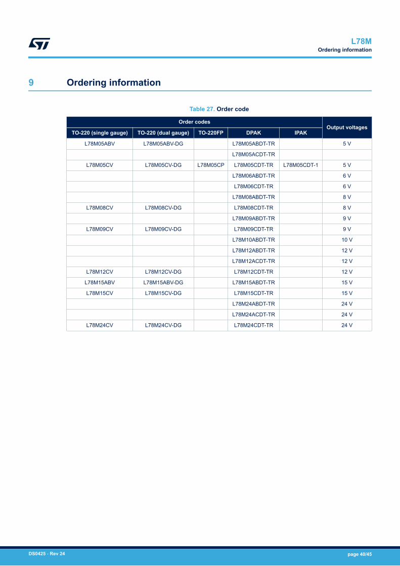
9 Ordering information
Table 27. Order code
Order codesOutput voltages
TO-220 (single gauge) TO-220 (dual gauge) TO-220FP DPAK IPAK
L78M05ABV L78M05ABV-DG L78M05ABDT-TR 5 V
L78M05ACDT-TR
L78M05CV L78M05CV-DG L78M05CP L78M05CDT-TR L78M05CDT-1 5 V
L78M06ABDT-TR 6 V
L78M06CDT-TR 6 V
L78M08ABDT-TR 8 V
L78M08CV L78M08CV-DG L78M08CDT-TR 8 V
L78M09ABDT-TR 9 V
L78M09CV L78M09CV-DG L78M09CDT-TR 9 V
L78M10ABDT-TR 10 V
L78M12ABDT-TR 12 V
L78M12ACDT-TR 12 V
L78M12CV L78M12CV-DG L78M12CDT-TR 12 V
L78M15ABV L78M15ABV-DG L78M15ABDT-TR 15 V
L78M15CV L78M15CV-DG L78M15CDT-TR 15 V
L78M24ABDT-TR 24 V
L78M24ACDT-TR 24 V
L78M24CV L78M24CV-DG L78M24CDT-TR 24 V
L78MOrdering information
DS0425 - Rev 24 page 40/45
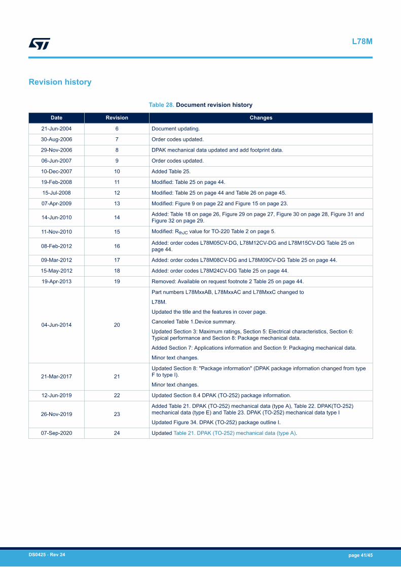
Revision history
Table 28. Document revision history
Date Revision Changes
21-Jun-2004 6 Document updating.
30-Aug-2006 7 Order codes updated.
29-Nov-2006 8 DPAK mechanical data updated and add footprint data.
06-Jun-2007 9 Order codes updated.
10-Dec-2007 10 Added Table 25.
19-Feb-2008 11 Modified: Table 25 on page 44.
15-Jul-2008 12 Modified: Table 25 on page 44 and Table 26 on page 45.
07-Apr-2009 13 Modified: Figure 9 on page 22 and Figure 15 on page 23.
14-Jun-2010 14 Added: Table 18 on page 26, Figure 29 on page 27, Figure 30 on page 28, Figure 31 andFigure 32 on page 29.
11-Nov-2010 15 Modified: RthJC value for TO-220 Table 2 on page 5.
08-Feb-2012 16 Added: order codes L78M05CV-DG, L78M12CV-DG and L78M15CV-DG Table 25 onpage 44.
09-Mar-2012 17 Added: order codes L78M08CV-DG and L78M09CV-DG Table 25 on page 44.
15-May-2012 18 Added: order codes L78M24CV-DG Table 25 on page 44.
19-Apr-2013 19 Removed: Available on request footnote 2 Table 25 on page 44.
04-Jun-2014 20
Part numbers L78MxxAB, L78MxxAC and L78MxxC changed to
L78M.
Updated the title and the features in cover page.
Canceled Table 1.Device summary.
Updated Section 3: Maximum ratings, Section 5: Electrical characteristics, Section 6:Typical performance and Section 8: Package mechanical data.
Added Section 7: Applications information and Section 9: Packaging mechanical data.
Minor text changes.
21-Mar-2017 21Updated Section 8: "Package information" (DPAK package information changed from typeF to type I).
Minor text changes.
12-Jun-2019 22 Updated Section 8.4 DPAK (TO-252) package information.
26-Nov-2019 23Added Table 21. DPAK (TO-252) mechanical data (type A), Table 22. DPAK(TO-252)mechanical data (type E) and Table 23. DPAK (TO-252) mechanical data type I
Updated Figure 34. DPAK (TO-252) package outline I.
07-Sep-2020 24 Updated Table 21. DPAK (TO-252) mechanical data (type A).
L78M
DS0425 - Rev 24 page 41/45
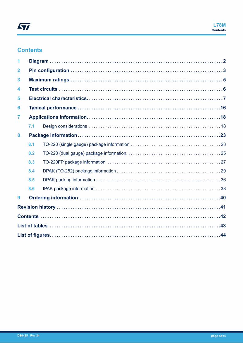
Contents
1 Diagram . . . . . . . . . . . . . . . . . . . . . . . . . . . . . . . . . . . . . . . . . . . . . . . . . . . . . . . . . . . . . . . . . . . . . . . . . . .2
2 Pin configuration . . . . . . . . . . . . . . . . . . . . . . . . . . . . . . . . . . . . . . . . . . . . . . . . . . . . . . . . . . . . . . . . . .3
3 Maximum ratings . . . . . . . . . . . . . . . . . . . . . . . . . . . . . . . . . . . . . . . . . . . . . . . . . . . . . . . . . . . . . . . . . .5
4 Test circuits . . . . . . . . . . . . . . . . . . . . . . . . . . . . . . . . . . . . . . . . . . . . . . . . . . . . . . . . . . . . . . . . . . . . . . .6
5 Electrical characteristics. . . . . . . . . . . . . . . . . . . . . . . . . . . . . . . . . . . . . . . . . . . . . . . . . . . . . . . . . . .7
6 Typical performance . . . . . . . . . . . . . . . . . . . . . . . . . . . . . . . . . . . . . . . . . . . . . . . . . . . . . . . . . . . . . .16
7 Applications information. . . . . . . . . . . . . . . . . . . . . . . . . . . . . . . . . . . . . . . . . . . . . . . . . . . . . . . . . .18
7.1 Design considerations . . . . . . . . . . . . . . . . . . . . . . . . . . . . . . . . . . . . . . . . . . . . . . . . . . . . . . . . . 18
8 Package information. . . . . . . . . . . . . . . . . . . . . . . . . . . . . . . . . . . . . . . . . . . . . . . . . . . . . . . . . . . . . .23
8.1 TO-220 (single gauge) package information . . . . . . . . . . . . . . . . . . . . . . . . . . . . . . . . . . . . . . . 23
8.2 TO-220 (dual gauge) package information. . . . . . . . . . . . . . . . . . . . . . . . . . . . . . . . . . . . . . . . . 25
8.3 TO-220FP package information . . . . . . . . . . . . . . . . . . . . . . . . . . . . . . . . . . . . . . . . . . . . . . . . . 27
8.4 DPAK (TO-252) package information . . . . . . . . . . . . . . . . . . . . . . . . . . . . . . . . . . . . . . . . . . . . . 29
8.5 DPAK packing information . . . . . . . . . . . . . . . . . . . . . . . . . . . . . . . . . . . . . . . . . . . . . . . . . . . . . . 36
8.6 IPAK package information . . . . . . . . . . . . . . . . . . . . . . . . . . . . . . . . . . . . . . . . . . . . . . . . . . . . . . 38
9 Ordering information . . . . . . . . . . . . . . . . . . . . . . . . . . . . . . . . . . . . . . . . . . . . . . . . . . . . . . . . . . . . .40
Revision history . . . . . . . . . . . . . . . . . . . . . . . . . . . . . . . . . . . . . . . . . . . . . . . . . . . . . . . . . . . . . . . . . . . . . . .41
Contents . . . . . . . . . . . . . . . . . . . . . . . . . . . . . . . . . . . . . . . . . . . . . . . . . . . . . . . . . . . . . . . . . . . . . . . . . . . . . .42
List of tables . . . . . . . . . . . . . . . . . . . . . . . . . . . . . . . . . . . . . . . . . . . . . . . . . . . . . . . . . . . . . . . . . . . . . . . . . .43
List of figures. . . . . . . . . . . . . . . . . . . . . . . . . . . . . . . . . . . . . . . . . . . . . . . . . . . . . . . . . . . . . . . . . . . . . . . . . .44
L78MContents
DS0425 - Rev 24 page 42/45
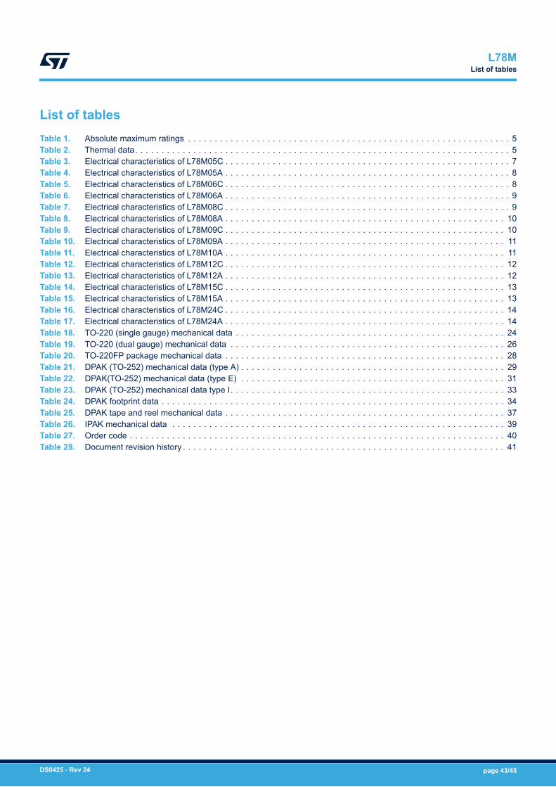
List of tablesTable 1. Absolute maximum ratings . . . . . . . . . . . . . . . . . . . . . . . . . . . . . . . . . . . . . . . . . . . . . . . . . . . . . . . . . . . . . 5Table 2. Thermal data. . . . . . . . . . . . . . . . . . . . . . . . . . . . . . . . . . . . . . . . . . . . . . . . . . . . . . . . . . . . . . . . . . . . . . . 5Table 3. Electrical characteristics of L78M05C . . . . . . . . . . . . . . . . . . . . . . . . . . . . . . . . . . . . . . . . . . . . . . . . . . . . . . 7Table 4. Electrical characteristics of L78M05A . . . . . . . . . . . . . . . . . . . . . . . . . . . . . . . . . . . . . . . . . . . . . . . . . . . . . . 8Table 5. Electrical characteristics of L78M06C . . . . . . . . . . . . . . . . . . . . . . . . . . . . . . . . . . . . . . . . . . . . . . . . . . . . . . 8Table 6. Electrical characteristics of L78M06A . . . . . . . . . . . . . . . . . . . . . . . . . . . . . . . . . . . . . . . . . . . . . . . . . . . . . . 9Table 7. Electrical characteristics of L78M08C . . . . . . . . . . . . . . . . . . . . . . . . . . . . . . . . . . . . . . . . . . . . . . . . . . . . . . 9Table 8. Electrical characteristics of L78M08A . . . . . . . . . . . . . . . . . . . . . . . . . . . . . . . . . . . . . . . . . . . . . . . . . . . . . 10Table 9. Electrical characteristics of L78M09C . . . . . . . . . . . . . . . . . . . . . . . . . . . . . . . . . . . . . . . . . . . . . . . . . . . . . 10Table 10. Electrical characteristics of L78M09A . . . . . . . . . . . . . . . . . . . . . . . . . . . . . . . . . . . . . . . . . . . . . . . . . . . . . 11Table 11. Electrical characteristics of L78M10A . . . . . . . . . . . . . . . . . . . . . . . . . . . . . . . . . . . . . . . . . . . . . . . . . . . . . 11Table 12. Electrical characteristics of L78M12C . . . . . . . . . . . . . . . . . . . . . . . . . . . . . . . . . . . . . . . . . . . . . . . . . . . . . 12Table 13. Electrical characteristics of L78M12A . . . . . . . . . . . . . . . . . . . . . . . . . . . . . . . . . . . . . . . . . . . . . . . . . . . . . 12Table 14. Electrical characteristics of L78M15C . . . . . . . . . . . . . . . . . . . . . . . . . . . . . . . . . . . . . . . . . . . . . . . . . . . . . 13Table 15. Electrical characteristics of L78M15A . . . . . . . . . . . . . . . . . . . . . . . . . . . . . . . . . . . . . . . . . . . . . . . . . . . . . 13Table 16. Electrical characteristics of L78M24C . . . . . . . . . . . . . . . . . . . . . . . . . . . . . . . . . . . . . . . . . . . . . . . . . . . . . 14Table 17. Electrical characteristics of L78M24A . . . . . . . . . . . . . . . . . . . . . . . . . . . . . . . . . . . . . . . . . . . . . . . . . . . . . 14Table 18. TO-220 (single gauge) mechanical data . . . . . . . . . . . . . . . . . . . . . . . . . . . . . . . . . . . . . . . . . . . . . . . . . . . 24Table 19. TO-220 (dual gauge) mechanical data . . . . . . . . . . . . . . . . . . . . . . . . . . . . . . . . . . . . . . . . . . . . . . . . . . . . 26Table 20. TO-220FP package mechanical data . . . . . . . . . . . . . . . . . . . . . . . . . . . . . . . . . . . . . . . . . . . . . . . . . . . . . 28Table 21. DPAK (TO-252) mechanical data (type A) . . . . . . . . . . . . . . . . . . . . . . . . . . . . . . . . . . . . . . . . . . . . . . . . . . 29Table 22. DPAK(TO-252) mechanical data (type E) . . . . . . . . . . . . . . . . . . . . . . . . . . . . . . . . . . . . . . . . . . . . . . . . . . 31Table 23. DPAK (TO-252) mechanical data type I. . . . . . . . . . . . . . . . . . . . . . . . . . . . . . . . . . . . . . . . . . . . . . . . . . . . 33Table 24. DPAK footprint data . . . . . . . . . . . . . . . . . . . . . . . . . . . . . . . . . . . . . . . . . . . . . . . . . . . . . . . . . . . . . . . . . 34Table 25. DPAK tape and reel mechanical data . . . . . . . . . . . . . . . . . . . . . . . . . . . . . . . . . . . . . . . . . . . . . . . . . . . . . 37Table 26. IPAK mechanical data . . . . . . . . . . . . . . . . . . . . . . . . . . . . . . . . . . . . . . . . . . . . . . . . . . . . . . . . . . . . . . . 39Table 27. Order code . . . . . . . . . . . . . . . . . . . . . . . . . . . . . . . . . . . . . . . . . . . . . . . . . . . . . . . . . . . . . . . . . . . . . . . 40Table 28. Document revision history . . . . . . . . . . . . . . . . . . . . . . . . . . . . . . . . . . . . . . . . . . . . . . . . . . . . . . . . . . . . . 41
L78MList of tables
DS0425 - Rev 24 page 43/45
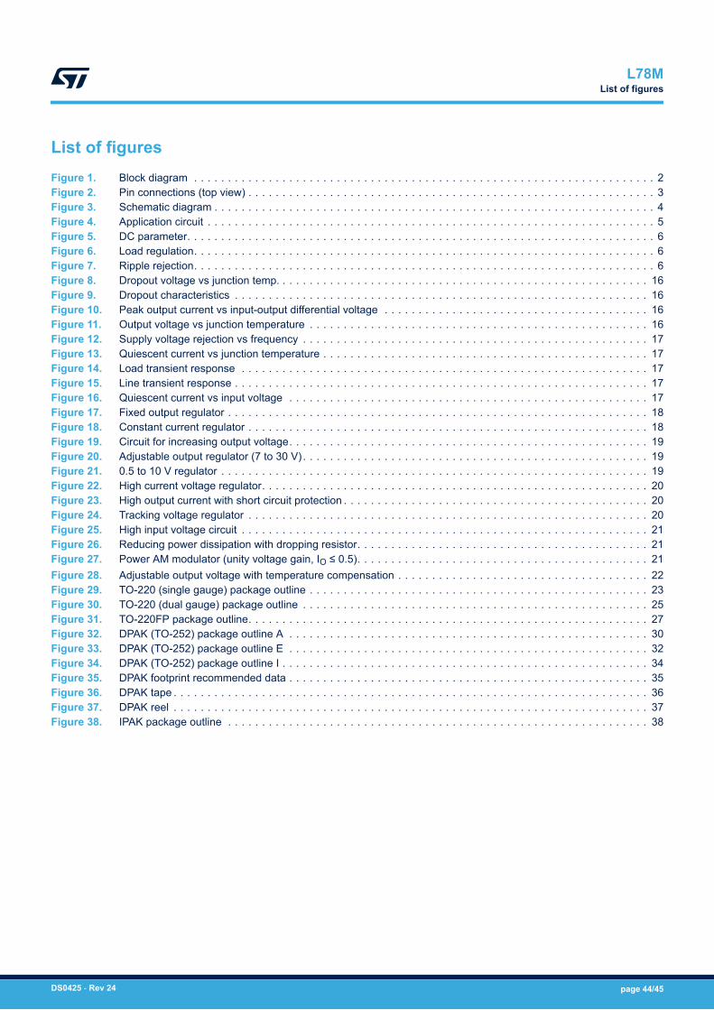
List of figuresFigure 1. Block diagram . . . . . . . . . . . . . . . . . . . . . . . . . . . . . . . . . . . . . . . . . . . . . . . . . . . . . . . . . . . . . . . . . . . . 2Figure 2. Pin connections (top view) . . . . . . . . . . . . . . . . . . . . . . . . . . . . . . . . . . . . . . . . . . . . . . . . . . . . . . . . . . . . 3Figure 3. Schematic diagram . . . . . . . . . . . . . . . . . . . . . . . . . . . . . . . . . . . . . . . . . . . . . . . . . . . . . . . . . . . . . . . . . 4Figure 4. Application circuit . . . . . . . . . . . . . . . . . . . . . . . . . . . . . . . . . . . . . . . . . . . . . . . . . . . . . . . . . . . . . . . . . . 5Figure 5. DC parameter. . . . . . . . . . . . . . . . . . . . . . . . . . . . . . . . . . . . . . . . . . . . . . . . . . . . . . . . . . . . . . . . . . . . . 6Figure 6. Load regulation. . . . . . . . . . . . . . . . . . . . . . . . . . . . . . . . . . . . . . . . . . . . . . . . . . . . . . . . . . . . . . . . . . . . 6Figure 7. Ripple rejection. . . . . . . . . . . . . . . . . . . . . . . . . . . . . . . . . . . . . . . . . . . . . . . . . . . . . . . . . . . . . . . . . . . . 6Figure 8. Dropout voltage vs junction temp. . . . . . . . . . . . . . . . . . . . . . . . . . . . . . . . . . . . . . . . . . . . . . . . . . . . . . . 16Figure 9. Dropout characteristics . . . . . . . . . . . . . . . . . . . . . . . . . . . . . . . . . . . . . . . . . . . . . . . . . . . . . . . . . . . . . 16Figure 10. Peak output current vs input-output differential voltage . . . . . . . . . . . . . . . . . . . . . . . . . . . . . . . . . . . . . . . 16Figure 11. Output voltage vs junction temperature . . . . . . . . . . . . . . . . . . . . . . . . . . . . . . . . . . . . . . . . . . . . . . . . . . 16Figure 12. Supply voltage rejection vs frequency . . . . . . . . . . . . . . . . . . . . . . . . . . . . . . . . . . . . . . . . . . . . . . . . . . . 17Figure 13. Quiescent current vs junction temperature . . . . . . . . . . . . . . . . . . . . . . . . . . . . . . . . . . . . . . . . . . . . . . . . 17Figure 14. Load transient response . . . . . . . . . . . . . . . . . . . . . . . . . . . . . . . . . . . . . . . . . . . . . . . . . . . . . . . . . . . . 17Figure 15. Line transient response . . . . . . . . . . . . . . . . . . . . . . . . . . . . . . . . . . . . . . . . . . . . . . . . . . . . . . . . . . . . . 17Figure 16. Quiescent current vs input voltage . . . . . . . . . . . . . . . . . . . . . . . . . . . . . . . . . . . . . . . . . . . . . . . . . . . . . 17Figure 17. Fixed output regulator . . . . . . . . . . . . . . . . . . . . . . . . . . . . . . . . . . . . . . . . . . . . . . . . . . . . . . . . . . . . . . 18Figure 18. Constant current regulator . . . . . . . . . . . . . . . . . . . . . . . . . . . . . . . . . . . . . . . . . . . . . . . . . . . . . . . . . . . 18Figure 19. Circuit for increasing output voltage. . . . . . . . . . . . . . . . . . . . . . . . . . . . . . . . . . . . . . . . . . . . . . . . . . . . . 19Figure 20. Adjustable output regulator (7 to 30 V) . . . . . . . . . . . . . . . . . . . . . . . . . . . . . . . . . . . . . . . . . . . . . . . . . . . 19Figure 21. 0.5 to 10 V regulator . . . . . . . . . . . . . . . . . . . . . . . . . . . . . . . . . . . . . . . . . . . . . . . . . . . . . . . . . . . . . . . 19Figure 22. High current voltage regulator. . . . . . . . . . . . . . . . . . . . . . . . . . . . . . . . . . . . . . . . . . . . . . . . . . . . . . . . . 20Figure 23. High output current with short circuit protection . . . . . . . . . . . . . . . . . . . . . . . . . . . . . . . . . . . . . . . . . . . . . 20Figure 24. Tracking voltage regulator . . . . . . . . . . . . . . . . . . . . . . . . . . . . . . . . . . . . . . . . . . . . . . . . . . . . . . . . . . . 20Figure 25. High input voltage circuit . . . . . . . . . . . . . . . . . . . . . . . . . . . . . . . . . . . . . . . . . . . . . . . . . . . . . . . . . . . . 21Figure 26. Reducing power dissipation with dropping resistor. . . . . . . . . . . . . . . . . . . . . . . . . . . . . . . . . . . . . . . . . . . 21Figure 27. Power AM modulator (unity voltage gain, IO ≤ 0.5). . . . . . . . . . . . . . . . . . . . . . . . . . . . . . . . . . . . . . . . . . . 21Figure 28. Adjustable output voltage with temperature compensation . . . . . . . . . . . . . . . . . . . . . . . . . . . . . . . . . . . . . 22Figure 29. TO-220 (single gauge) package outline . . . . . . . . . . . . . . . . . . . . . . . . . . . . . . . . . . . . . . . . . . . . . . . . . . 23Figure 30. TO-220 (dual gauge) package outline . . . . . . . . . . . . . . . . . . . . . . . . . . . . . . . . . . . . . . . . . . . . . . . . . . . 25Figure 31. TO-220FP package outline. . . . . . . . . . . . . . . . . . . . . . . . . . . . . . . . . . . . . . . . . . . . . . . . . . . . . . . . . . . 27Figure 32. DPAK (TO-252) package outline A . . . . . . . . . . . . . . . . . . . . . . . . . . . . . . . . . . . . . . . . . . . . . . . . . . . . . 30Figure 33. DPAK (TO-252) package outline E . . . . . . . . . . . . . . . . . . . . . . . . . . . . . . . . . . . . . . . . . . . . . . . . . . . . . 32Figure 34. DPAK (TO-252) package outline I . . . . . . . . . . . . . . . . . . . . . . . . . . . . . . . . . . . . . . . . . . . . . . . . . . . . . . 34Figure 35. DPAK footprint recommended data . . . . . . . . . . . . . . . . . . . . . . . . . . . . . . . . . . . . . . . . . . . . . . . . . . . . . 35Figure 36. DPAK tape . . . . . . . . . . . . . . . . . . . . . . . . . . . . . . . . . . . . . . . . . . . . . . . . . . . . . . . . . . . . . . . . . . . . . . 36Figure 37. DPAK reel . . . . . . . . . . . . . . . . . . . . . . . . . . . . . . . . . . . . . . . . . . . . . . . . . . . . . . . . . . . . . . . . . . . . . . 37Figure 38. IPAK package outline . . . . . . . . . . . . . . . . . . . . . . . . . . . . . . . . . . . . . . . . . . . . . . . . . . . . . . . . . . . . . . 38
L78MList of figures
DS0425 - Rev 24 page 44/45
IMPORTANT NOTICE – PLEASE READ CAREFULLY
STMicroelectronics NV and its subsidiaries (“ST”) reserve the right to make changes, corrections, enhancements, modifications, and improvements to STproducts and/or to this document at any time without notice. Purchasers should obtain the latest relevant information on ST products before placing orders. STproducts are sold pursuant to ST’s terms and conditions of sale in place at the time of order acknowledgement.
Purchasers are solely responsible for the choice, selection, and use of ST products and ST assumes no liability for application assistance or the design ofPurchasers’ products.
No license, express or implied, to any intellectual property right is granted by ST herein.
Resale of ST products with provisions different from the information set forth herein shall void any warranty granted by ST for such product.
ST and the ST logo are trademarks of ST. For additional information about ST trademarks, please refer to www.st.com/trademarks. All other product or servicenames are the property of their respective owners.
Information in this document supersedes and replaces information previously supplied in any prior versions of this document.
© 2020 STMicroelectronics – All rights reserved
L78M
DS0425 - Rev 24 page 45/45