Embed Size (px)
Citation preview

Defect structure and strain reduction of 3C-SiC/Si layers obtained with the use
of buffer layer and methyltrichlorosilane addition
M. Bosi 1,*, G. Attolini 1, M. Negri 1, C. Ferrari 1, E. Buffagni 1, C. Frigeri 1, M. Calicchio1, B. Pécz
2, F. Riesz 2 , I. Cora 2, Z. Osváth2, L. Jiang3 , G. Borionetti4
1 IMEM-CNR, Parco Area delle Scienze 37 A, 43124 Parma, Italy
2 Institute for Technical Physics and Materials Science, Centre for Energy Research, Hungarian
Academy of Sciences, P.O.Box 49, H-1525 Budapest, Hungary
3 Engineering Sciences, Faculty of Engineering and the Environment, University of Southampton,
Highfield, Southampton SO17 1BJ, United Kingdom
4 MEMC Electronic Materials S.p.A., Viale Gherzi 31, 28100 Novara, Italy
corresponding author: * [email protected] (+39 0521 269288)
Abstract
3C-SiC layers were deposited on Si substrates by using a low temperature buffer layer and the
addition of methyl trichloro silane (MTS) to the gas phase during the high temperature thick film
growth. Several samples were grown by varying the deposition temperature and the MTS content in
order to study how these parameters affect the layer quality and the lattice defects. All of the grown
layers are single crystalline and epitaxial to the substrate. The formation of empty voids at the
SiC/Si interface was successfully avoided. The surface of the layers grown with MTS addition was
smoother and contained less residual strain. A 15 m thick 3C-SiC sample was grown with an
optimized process in order to evaluate its residual strain and bow.

Introduction
Cubic silicon carbide (-SiC or 3C-SiC) is a wide-bandgap semiconductor with high hardness, high
electron mobility, high thermal conductivity, high resistance to chemical attack and it is
biocompatible; for these reasons SiC is interesting for potential technological applications, such as
power devices and sensors operating in harsh environments. 1
Growth of 3C-SiC on Si substrates is attractive because the use of silicon substrates offers the
possibility to obtain large area SiC at low cost and to combine devices based on Si and SiC.
Moreover SiC can act as an etch mask during technological processes of Micro Electro Mechanical
Structures (MEMS) realization, permitting to fabricate advanced MEMS devices integrated with the
standard Si technology. 2,3
Many methods have been developed to grow 3C-SiC layers on Si substrate but conventional Vapor
Phase Epitaxy (VPE) using precursors such as silane and propane is still the most widely used
method. 4
The use of single-source precursors, such as monomethylsilane (CH3SiH3), MTS, tetramethylsilane
( (SiCH3)4 ), and hexamethyldisilane (Si2(CH3)6) have also been extensively studied for the
deposition of 3C-SiC thin films. 4,5 In all the alkyl compounds listed above a silicon-carbon bond is
contained, therefore they are considered more efficient than using silicon precursor + carbon
precursor. In most of the cases there are less safety issues to handle these compounds than silane, so
this was the first reason that pushed this research line. It is difficult to compare results about
crystalline quality found in literature, since the films are obtained under different growth conditions
(carbonization, buffer layer, growth temperature) and different characterization techniques are used
such as Atomic Force Microscopy (AFM), X-Ray Diffraction (XRD), Transmission Electron
Microscopy (TEM), Reflection High-Energy Electron Diffraction (RHEED), Low temperature
photoluminescence (LTPL), X-Ray Spectroscopy (XPS). Where the results are compared, no
significant improvement of the material quality is observed using single-source precursors. In

addition to that, the mobility on the substrate surface of a Si-C pair is lower than the single C or Si
adatoms, so the use of an single-source precursors doesn’t help in reducing the growth temperature.
By using an single-source precursors one might think that the carbon to silicon ratio is always
unitary, but it has been demonstrated 5 that secondary reactions induced by hydrogen reacting with
carbon deplete the carbon content of the gaseous phase, so best results are obtained adding a carbon
precursor to compensate that.
A common problem in SiC epitaxy is the tendency of Si to precipitate from the vapor, which can be
reduced by the use of halogenous precursors 6,7. Deposition processes using halogenous precursors
are interesting in order to enhance the film quality and growth rate in comparison with the standard
SiH4 and C3H8 mixtures as well. The main motivation is not only to prevent precipitation of Si, but
also to obtain thick 3C-SiC/Si film layers in a reasonable deposition time in order to reduce epitaxy
costs. It is also known that by increasing 3C-SiC thickness the layer structural properties improve,
and the addition of chlorine species to the gas phase permits to significantly increase the growth rate
without degrading the film properties 8. This behaviour is well known for 4H and 6H-SiC
homoepitaxy by adding HCl 9 but is still of limited use for 3C-SiC heteroepitaxy.
Although obtaining high-quality thick 3C-SiC layer is important for the realization of 3C-SiC
devices such as Schottky barriers 10 or sensor probes, 11 the main problem associated with achieving
state of the art, thick (higher than 4–5 μm) 3C-SiC epitaxy on Si is related to wafer warp or bow,
caused mainly by the large lattice mismatch (~20%) and the difference of thermal expansion
coefficient (~8%) between 3C-SiC film and Si substrate. For this reason, the development of a
process to grow thick 3C-SiC film on Si substrate with high throughput, high quality and low bow
is highly desirable.
In this paper we use MTS as the chlorinated species, mixed to propane and silane to grow a SiC
layer on Si (001) oriented substrates after the carburisation step. The films were characterised by
XRD, TEM and Makyoh topography.

The purpose of this work is to investigate how growth temperature, MTS addition, growth rate and
the growth process influence the defects and the strain of the 3C-SiC layers, in order to develop a
process to obtain layers with a low bow and good crystallographic quality.
Experimental
The 3C-SiC layers were deposited in a horizontal hot-wall VPE reactor without substrate rotation,
on (001) oriented Si substrates of about 2x5 cm2 size. We used MTS, SiH4, C3H8 as precursor,
diluted in 4000 sccm H2 as carrier gas. SiH4 flow was fixed at 3 sccm and the Si/H2 ratio was 7.5 x
10-4 for all the experiments. MTS was stored in a standard stainless steel bubbler for metal organics
liquids kept at 10 °C and 1200 mbar in a thermostatic bath. A controlled amount of MTS was
delivered to the growth chamber by the use of a standard double dilution metalorganic line.
Prior to growth, the Si wafers were etched in 10% HF:H2O (1:20) for 60 seconds to remove the
native oxide and were immediately loaded into the growth reactor. In order to reduce the stress in
the heteroepitaxial film we used a previously developed growth process as baseline and reference
for process improvement 12, that was further developed for this work with the addition of MTS to
the gas phase. The reference 3C-SiC/Si growth process consists of a carbonization step at 1125 °C
for 5 minutes, a heating ramp from 1125 °C to 1380 °C with both SiH4 and C3H8 to deposit a
stoichiometric buffer layer 12 and a thick film growth at 1380 °C using Si/C=1.4 in the gas phase,
with no MTS. The pressure during the carbonization was set at 700 mbar, while during the rest of
the process it was set at 200 mbar to reduce the tendency of SiH4 to react in the gas phase. This
reference layer was deeply analyzed in ref. 12 and it consisted of a high quality monocrystalline and
stoichiometric film.
In order to understand the effect of MTS addition to the gas phase we deposited several samples
using the reference conditions explained above and adding an MTS flow between 0.15 and 6 sccm.
During these experiments we also tested a growth by using MTS only at 1380 °C, with no addition

of either SiH4 or C3H8 but it resulted in a film with a very hazy surface, and the XRD analysis does
not indicate the presence of any peak, indicating that the layer was probably amorphous.
Starting from the reference process without the addition of MTS, we also deposited films at
different temperatures (1300 °C, 1350°C, 1380 °C, 1400 °C) and then investigated how the addition
of a fixed amount of MTS with flow of 0.3 sccm (Flow(MTS)/Flow(SiH4) = 1/10) influences the
growth at these temperatures. In order to be sure that the observed differences are ascribed to the
thick SiC layer only and not to a different buffer layer pre-growth process, we maintained the same
buffer layer deposited for the standard sample, but changed the growth temperature with a fast ramp
in H2 only after the reactor reached 1380 °C. The schematics of this growth processes are illustrated
in Fig. 1. Growth time was set to 30 minutes for all samples.
To test the effectiveness of the growth procedure developed with MTS and to check the wafer bow
induced by a thick SiC layer, we performed an additional growth at 1380 °C with MTS flow = 0.6
sccm and with doubled 6 sccm SiH4 with respect to the previous experiments, lasting 3 hours in
total and resulting in an about 15 m thick 3C-SiC layer. For this sample, in order to reduce the
thickness gradient and to obtain a more homogeneous SiC layer, we performed the growth in two
different steps: the first part was a standard growth (including the carbonization and buffer) at 1380
°C lasting for 90 minutes. After this first deposition, the wafer was extracted from the growth
chamber, rotated 180° and immediately reinserted in the same position. The second part of the
growth lasted another 90 minutes and consisted of the deposition of the SiC film only, with the
same precursors and partial pressures as the first part but without the pre-growth procedures such as
carbonization and buffer layer. By performing this two-step process we were able to compensate the
thickness gradient along the flow direction and to obtain a more homogeneous sample with a
thickness variation of about 3% over the whole area.

Fig. 1: Schematic of the growth process. Time is not in scale for the different parts of the process.
XRD was obtained with a custom modified Philips X-Ray diffractometer using Cu Kα radiation and
a Göbel mirror to investigate the (002) reflection of SiC.
Observations by TEMwere carried out on cross sectional specimens by using a Philips CM20
microscope and a JEOL-2200FS TEM-STEM field emission gun (FEG) both working at 200 keV.
The JEOL was equipped with a HAADF (High Angle Annular Dark Field) detector and operated in
the STEM (Scanning TEM) mode. The STEM-HAADF pictures were taken with a camera length of
100 mm and a spot size of 0.7 nm. At such camera length the collection angle is smaller than the
one of typical HAADF and we shall use the more generic ADF (Annular Dark Field) acronym in
the following. Furthermore some high resolution images were taken in a JEOL 3010 microscope at
300kV.
We also analyzed the samples by means of grid-projection Makyoh topography 13 in order to study
the sample bending.
Film thickness was measured by means of optical reflectivity in the 400-1100 nm range.
Samples were additionally investigated by confocal Raman spectroscopy performed on a WiTec
alpha300 RSA microscope using an excitation laser of 532 nm. Several thousands of spectra were
measured on each sample, acquired on areas of 20x20 m.

3. Results and discussion
3.1. Crystalline quality
A well-known consequence of the horizontal geometry of an epitaxial reactor is the observation of a
thickness gradient, due to depletion of silane downstream in the chamber. 14 At fixed temperature of
1380 °C a change in the growth rate is evident after the addition of MTS in the gas phase (Fig. 2):
the points were tentatively fitted with an exponential curve, and we can hypothesize that the growth
rate would reach a plateau for higher MTS flows. From the thickness measurement of the different
samples in the same position it is noted that even an addition of 0.15 sccm of MTS to the gas phase
( F(MTS)/F(SiH4) = 1/20 ) is sufficient to increase the growth rate by about 50%. The saturation
observed at higher MTS flows could indicate that most of the Si supplied in the gas phase is
actually incorporated in the film, without formation of Si droplets or aggregates, indicating that the
growth in these conditions is mainly limited by mass transport.
XRD data of selected samples obtained in different positions with the same thickness, but with
different growth rates, are shown in Fig. 3: only the (002) reflection of 3C-SiC is present, indicating
the monocrystallinity of the epitaxial layer. The (002) peak of all the samples analysed is at
2B=45.39±0.02° which is in agreement with the lattice parameter of 3C-SiC=4.3596 Å. The
FWHM of this peak is slightly decreasing with the addition of an MTS flow of 0.3 sccm, while for
the sample with MTS=6 sccm the FWHM increases.
TEM images of selected samples were acquired in order to have a deeper understanding of this
behavior and to get a better understanding of the lattice structure. TEM analysis of a reference
sample grown without the addition of MTS was already reported in ref 12 and it is not included in
this discussion. In Fig. 4 two samples are investigated: Fig. 4a shows the layer grown with an MTS
flow of 3 sccm. The diffraction pattern in the inset shows a complete epitaxial registry between SiC

and Si. Although there are stacking faults in the layer, their density is low, therefore the streaks in
the diffraction pattern are almost invisible. In contrast, Fig. 4b shows the layer grown with MTS
flow of 0.15 sccm. Some streaks are observed in the diffraction pattern and this layer contains a
higher density of crystal defects than the previous one, leading to conclude that the use of a higher
MTS flow, up to MTS flow of 3 sccm, permits to slightly increase the lattice quality, while reaching
flow values near 6 sccm degrades it, as observed by XRD. The image presented in Fig. 4a, with
MTS flow of 3 sccm, shows contrast fringes at the interface inside the silicon substrate crystal due
to local strain.The fact that this is completely missing in Fig. 4b suggests that the strain, in the case
of higher growth rate, is rapidly relieved near the interface by lattice defects, i.e. misfit dislocations
and stacking faults, whereas this mechanism is not so efficient in case of lower growth rate. Point
defects can also contribute to relieve the strain, like vacancies for compressively strained layers,
like Ge/Si15 or SiGe/Si16, or interstitials for the tensile strain case17. In the tensile SiC/Si system
Osten et al. have suggested that strain relaxation can partially be due to C interstitials alone or
bound to a second substitutional C atom18. Point defects may give rise to stacking faults whose
partial dislocations can further relieve the strain. This latter contribution to the strain relaxation,
however, in our case should be much smaller than the one associated with the stacking faults
generated by the misfit dislocations dissociation which typically occurs and prevails in systems
under tensile stress19. Increasing the MTS partial pressure to higher value would mean to introduce
even more lattice defects, probably given by the very high growth rate, that lead to the degradation
observed by XRD.

0 1 2
40
60
80
100
120
MTS flow (sccm)
G
row
th r
ate
(n
m/m
in)
MTS/SiH4 ratio
0 3 6
Fig. 2 Growth rate depending on MTS flow. The line is drawn as a guide to the eye.
38 39 40 41 42 43 44 4510
100
1000
10000
100000
1000000
1E7
1E8
B: MTS flow = 0.3 sccm
FWHM = 810 arcsec
A: MTS flow = 0
FWHM = 850 arcsec
Inte
nsity (
A.U
.)
2 (degrees)
C: MTS flow = 6 sccm
FWHM = 950 arcsec
Fig. 3 XRD patterns of selected samples grown with different MTS flow. The curves for samples B and C are vertically
shifted 10x and 100x times, respectively, for clarity.
a)
b)
Fig. 4 TEM images of samples grown with MTS flow of: A=3 sccm, B=0.15 sccm
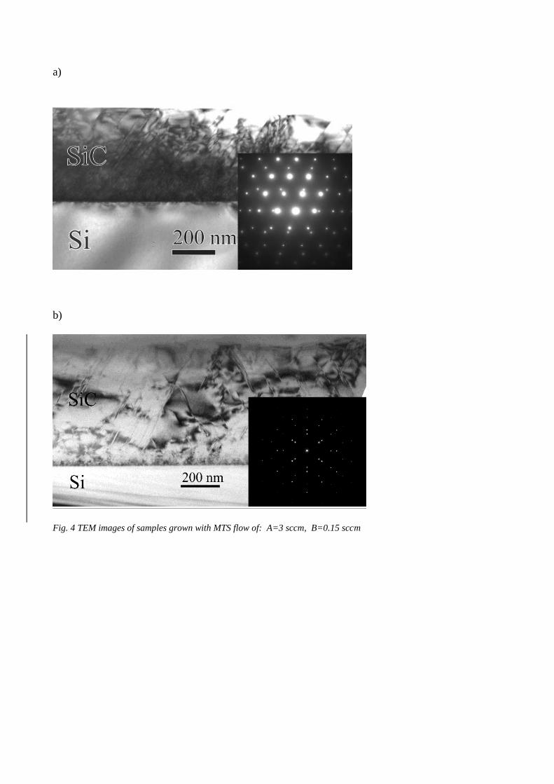
3.2. Growth rate, thickness gradient and crystal quality
Fig. 5 shows the thickness measured along the whole wafer for samples grown at different
temperatures, with and without the addition of MTS with constant MTS flow of 0.3 sccm for all
samples and with the same growth time (30 min). Several observations can be made about the slope
of the thickness gradient,the total thickness of the samples, and the growth rate for the different
samples, calculated as thickness / growth time at the same position over the susceptor.
1000
2000
3000
1300 °C
1300 °C + MTS
1350°C
1350°C + MTS
1380°C
1380°C + MTS
1400°C
1400°C + MTS
Thic
kness (
nm
)
Position on the susceptor (mm)gas inlet gas outlet
0 20 40
Fig. 5: Thickness measured for different samples in different positions along the graphite susceptor.
First of all, the two samples grown at 1300 °C have a lower growth rate with respect to the other
ones, indicating that the growth regime at this temperature is still limited by reaction kinetics: the
available energy given by temperature may not be enough to break the bonds of all SiH4 molecules
or to activate surface reactions that lead to the growth. Surface mobility of adsorbed species may
also be lower. In this regime, the growth rate is not controlled by the SiH4 flow delivered to the
growth chamber but by the temperature 20. The fact that the growth rate increases with MTS
addition reveals that Si radicals in MTS molecules may be easily dissociated to let more Si become
available for surface incorporation. It is also interesting to observe that, since the ratio between

MTS and SiH4 flow is 1/10, the increase of the growth rate could not be totally attributed to the
additional Si radicals delivered by MTS. Other reaction mechanisms, governed by reaction kinetics
and the presence of chlorinated species, may be also involved in the increase of the growth rate at
this temperature.
At temperatures higher than 1350 °C the growth rate for all other samples (considering separately
the one with or without MTS addition) is very similar and for the growths at 1380 and 1400 °C is
practically the same. In these conditions all the available SiH4 could be considered dissociated and
the growth rate is limited by the SiH4 flow. The transition between the kinetic controlled regime and
the mass transport one could then be set between 1350 and 1380 °C. However, for the growth
without MTS, severe degradation was observed if the flow is increased beyond a certain threshold.
In our experimental apparatus, maintaining the same Si/C = 1.4, constant H2 flow and by not adding
MTS to the gas phase, we could not increase SiH4 over 3.5 sccm (with respect to the standard 3
sccm used in these experiments) without obtaining hazy and polycrystalline samples. This is a
common behavior observed in SiC growth, especially for 4H homoepitaxy 8 and it is attributed to
the tendency of Si to react in the gas phase, forming droplets and adducts that condense on the
substrate. The addition of MTS changes the gas-phase chemistry because chlorinated species bind
to Si atoms in the gas phase and prevents the formation of Si condensates 7: the Cl-Si bond has
lower energy with respect to Si-Si bond 21 and it does not form precipitates. In other growth
experiments with flow ratio between MTS and SiH4 as low as 1/10 the SiH4 flow could be increased
up to 6 sccm (with a linear increase of the growth rate) without any film degradation, as will be
discussed later.
The thickness gradient analysis indicates a higher depletion of silane in the gas phase at 1300 °C,
resulting in a more steep decrease of the growth rate along the susceptor length. The effect is
evident on both samples, with and without MTS, and it is reduced for the samples grown at
temperature higher than 1350 °C: for the other six samples the thickness gradient is very similar.
We have previously observed that the growth rate at 1300 °C depends mainly on temperature: the

observation of this strong thickness gradient for samples grown at this temperature may indicate a
different / higher temperature gradient in our growth chamber at these conditions, able to reduce the
silane dissociation and/or influencing reaction kinetics.
Fig. 6a reports the SiC (002) peaks FWHM as measured by XRD for the samples grown at different
temperatures with and without the addition of a fixed MTS amount. An error bar of +/- 15 arcsec
should be considered, given by the instrumental resolution. Normally the 3C-SiC layers crystal
quality increases with thickness, a behavior usually explained by the reduction of stacking defects
and microtwins due to their progressive annihilation during the growth. It is also recognized that,
while an increase of the 3C-SiC film thickness corresponds to reduction of XRD peak FWHM, a
growth rate increase for a fixed film thickness results in degradation of the quality, with a higher
FWHM22. This behaviour also aligns with our observation in (Fig. 3) that the XRD FWHM first
decreases when a low MTS flow (0.3 sccm) was used and then increases again when a high MTS
flow (6 sccm) was applied. This suggest that the increase in MTS flow significantly influences the
growth rate (Fig. 2).The introduction of MTS with low concentration (MTS flow=0.3 sccm, SiH4
flow = 3 sccm) slightly decreases the FWHM, indicating that these growth conditions may lead to
overall less defective layers. A systematic increase of lattice quality, with lower XRD peak FWHM,
is observed as thickness and deposition temperature increase.
In Fig. 6b the XRD peak FWHM of an additional sample 15 m thick is added. In our samples the
XRD FWHM scales almost linearly with the log10 of the thickness, indicating an improvement in
the crystal lattice as the thickness increase. Fig. 7 is the STEM-ADF image of the 15 µm thick
sample: in the ADF images taken with medium collection angle, the defects give bright contrast due
to the increased dechanneling 23,24. Fig. 7 shows that there is a very high density of crystal defects in
the first 0.15-0.20 µm of the layer immediately above the SiC/Si interface, as expected and
observed also for the samples discussed previously. The defects are stacking faults as confirmed by
SAD and High Resolution TEM images (not shown here). After this highly defective initial stripe
the density drastically reduces and keeps on reducing as the layer thickness increases, although with

a much smaller gradient. By taking as a reference the density of the defects at a distance of 0.2 µm
above the interface, i. e. just above the very defective stripe immediately above the interface, where
the defect counting was not possible, from Fig. 7 one can see that the defect density decreases at a
rate of about 13.4%/µm suggesting that the defects could be absent at layer thicknesses greater than
about 7.5 µm. The main mechanism of stacking fault reduction is probably by mutual annihilation.
The improvement of the crystal quality is thus evident from both XRD and TEM observations.
Nevertheless, with our procedure we do not obtain the same crystal quality observed in literature for
samples of similar thickness, reported with (002) peak FWHM as low as 250 arcsec 25.
Selected SiC layers shown in Fig. 5 were also investigated by TEM in cross section. In general the
images show that SiC is single crystalline and oriented on Si, as expected.

a)
500 1000 1500 2000 2500 3000 3500
750
800
850
900
950
1380 °C
1380 °C + MTS
1400 °C
1400 °C + MTS
XR
D F
WH
M (
arc
se
c)
thickness
1300 °C
1300 °C + MTS
1350 °C
1350 °C + MTS
b)
1000 10000600
650
700
750
800
850
900
950
1000
XR
D F
WH
M (
Arc
se
c)
thickness (nm)
Fig. 6: a) FWHM of (002) XRD peak for different samples. An error bar of about +/- 15 arcsec should be considered for
each point. For clarity, an additional sample with higher thickness was added in graph b). Note the log10 scale on the x
axis. The line is drawn as a guide for the eye.

Fig. 7 - STEM-ADF image of the SiC/Si sample 15 µm thick. The figure is a composition of two HAADF images. The
dark area at the top of the image is a very thick region not transparent to the electron beam.
The TEM images in Fig. 8 show the sample grown at 1400 °C with the addition of MTS. The single
crystalline SiC layer contains a lot of stacking faults, which give faint streaks in the diffraction
pattern. There is a huge density of defects at the SiC/Si interface, which is however, decreased
substantially toward the surface.
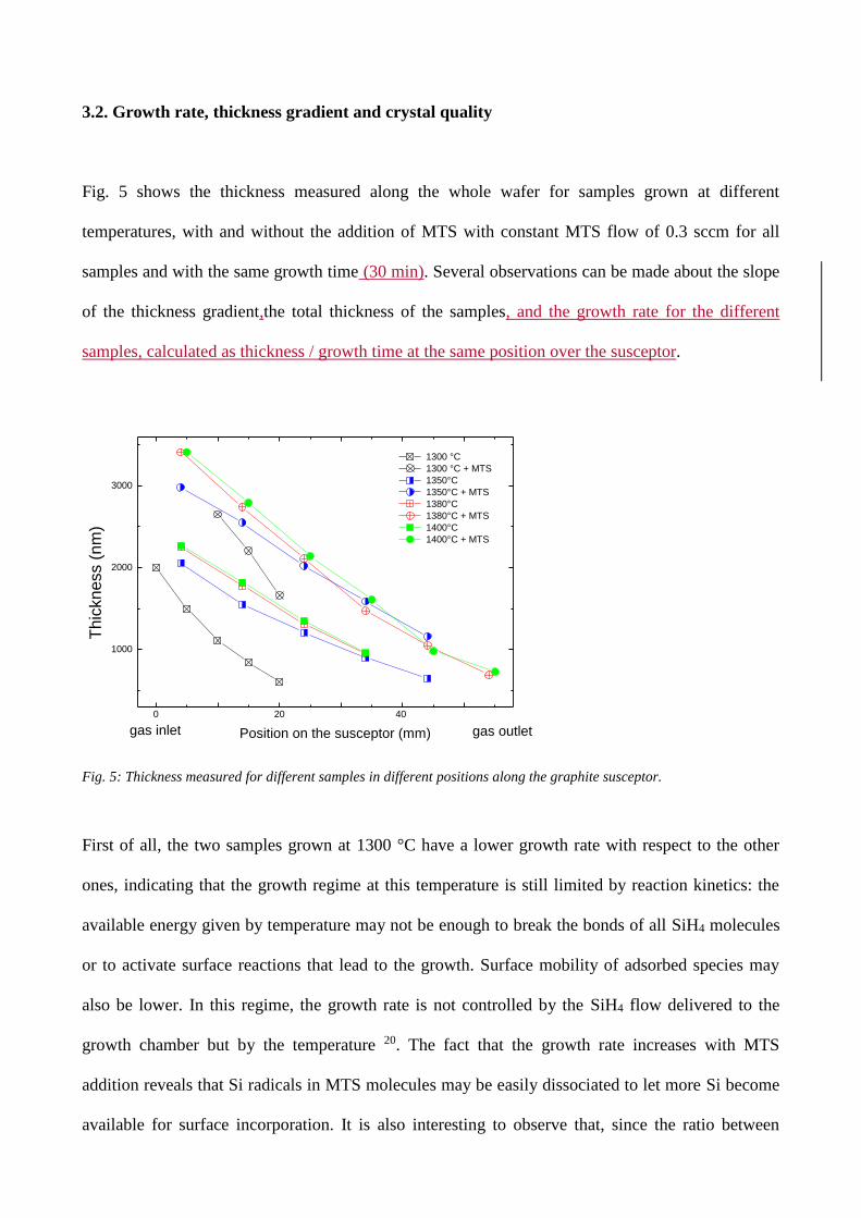
In Fig. 9 the sample grown at 1400 °C without the addition of MTS is shown. In this layer the
defect density is higher than the previous sample. Wavy lines with contrast variation are also
SiC

observed due to the two {111} stacking fault planes of the four which are out of the imaged zone.
The layer is single crystalline as well, but the defect density is not decreased so much like in the
former case toward the surface. Low magnification images had shown that the surface of the grown
SiC layer is not perfectly flat.
More detailed studies on this layer (Fig. 10) show that stacking faults are common in the lower part
of the 3C-SiC layer parallel to {111}. This is evident from the high resolution image in Fig. 10
insert E, which shows the stacking order across a typical stacking fault. No extended hexagonal
inclusions were found in the layer. However, as the stacking sequence is locally changed, there may
exist limited zones in the layer in which the cubic stacking is locally replaced with hexagonal one,
as observed in 3C-SiC nanowires 26,27. Although in all of the grown SiC layers the defect density is
high close to the silicon substrate, we observed that in layers grown with the addition of MTS (both
at 1300oC and at 1400oC) the defect density is substantially lowered towards the surface region.
Fig. 8 Bright field (left) and dark field (right) images taken on a sample grown with the addition of MTS. Diffraction
pattern is inserted to the middle of the above image.
Fig. 9 Selected area diffraction pattern (left) and bright field (right) images taken on a sample grown without the
addition of MTS.

Fig. 10 High resolution image of the interface between the Si substrate and the 3C-SiC layer in [1-10] projection. A, B
and C shows the indexed FFT images from the appropriate area in the white circles. The symmetry averaged images
with unit cell edges can be found next to the A and B FFTs. 3C-SiC was grown epitaxially onto Si(001). D: Filtered
IFFT of the interface shows misfit dislocations. Inset E shows a stacking fault in the SiC breaking the ccp stacking of
the 3C-SiC.

3.3. Strain and deformation
Fig. 11 reports the deformation profile for the 15 m sample, obtained by Makyoh topography.
Contrary to what commonly observed for thick 3C-SiC layers 25, and considering its high layer
thickness, the bow of our 15-m sample is very low. The sample is of saddle shape, with
approximate bow values of 4 m and 2 m along and perpendicular to the gas flow direction,
respectively. Considering the sample dimension of about 20 x 20 mm, these correspond to about 10
m and 20 m radii of curvature, respectively. These values represent a good improvement with
respect to samples, even with lower thickness, reported in literature 4,28, demonstrating that the
buffer procedure could be very effective in reducing the strain while maintaining a good
crystallographic quality. The saddle shape, although not expected based on simple symmetry
arguments, have been observed earlier in literature 29,30.
05
10
15
20
25
-0,004
-0,002
0,000
0,002
0,004
0,006
0
2
4
6
8
1012
1416
18
Heig
th (m
m)
Y p
osi
tion (
mm
)
X position (mm)
Fig. 11: Deformation profile for 15 m thick sample obtained by Makyoh topography

We argue that the higher XRD FWHM observed on our sample, with respect to other ones reported
in literature that usually present severe bow, indicates that the presence of extra lattice defects as
observed by TEM, located near the interface and generated during the buffer layer deposition 12, are
effectively able to relief the strain thus limiting wafer deformation. This may imply that with a low
defect density and high quality layer, as indicated by very low XRD FWHM, may be very difficult
to limit wafer curvature. The high density of defect located at the interface may also help the relief
of thermal strain between the thick SiC layer and the Si substrate during the cool down from high
temperature to room temperature. Moreover, with our procedure, it is also possible to considerably
reduce the voids at the interface between Si and SiC, commonly observed in literature 31. As it is
shown in all our TEM images, these defects are not characteristic of our layers.
Despite the lower crystal quality of the thick sample grown with our procedure with respect to the
best ones found in literature, certain SiC applications such as SiC MEMS sensors may benefit from
an optimal tradeoff between layer quality, sample thickness and substrate warp and
photolithographic /masking procedures may greatly benefit from a bow-free sample.
Raman analysis was also carried out on the two samples grown at 1400 °C with and without MTS,
and it is shown in Fig. 12. The TO peak values are 794.4 cm-1 and 794.2 cm-1 for the sample with
and without MTS, respectively, while the LO peak values are 970.2 cm-1 and 969.5 cm-1 , again for
the sample with and without MTS, respectively No modes relative to graphite, such as D (around
1355 cm-1) or G peaks (around 1596 cm-1), were observed in any Raman spectra.
The residual strain can be evaluated according to the model proposed by Olego et al. 32, based on
the spectral position of TO phonon peaks, since the LO peak shift depends also on the free-carrier
concentration.
The TO and LO peaks shift in dependence of the lattice mismatch a/a due to stress according to a
linear relation 32:
TO = 796.5 – (3734 ± 30) a/a

LO = 973 – (4532 ± 30) a/a
Considering the TO peak position obtained from the fitting we can estimate a tensile lattice strain
a/a in the film of about 0.05% ± 0.01%. A similar value (0,06% ± 0.01%) is obtained considering
the LO peak positions.
750 800 850 900 950 1000 1050
2000
4000
6000
Inte
nsity (
A.U
.)
Raman shift (cm-1)
1400 °C, with MTS
1400 °C, witout MTS
Fig. 12. Raman spectroscopy of samples shown in Fig. 8 (black line) and Fig. 9 (red line).
4. Conclusions
A 3C-SiC/Si growth procedure was used to reduce the formation of empty voids at the SiC/Si
interface. This process was further developed by the addition of MTS and it was shown how this
precursor influences the growth rate and crystal quality in dependence of its flow. The influence of
temperature and MTS flow on the growth rate and layer quality was studied, indicating that the
growth regime is limited by mass transport at temperatures higher than 1350 °C and limited by

reaction kinetics at lower temperatures. The samples grown with MTS addition show a better
crystal quality up to flow ratio between MTS and SiH4 of about 1. TEM analysis shows a lower
defect density of MTS samples with respect to samples grown without its addition, with better
quality near the surface region.
A 3C-SiC/Si with thickness of about 15 m was grown using the above mentioned procedure,
showing reduced bow with respect to samples reported in literature.

Acknowledgements
The authors are grateful to Mr. C. Mora for performing XRD measurements. B. Pécz thanks the
support of the Hungarian National Scientific Foundation (OTKA) through Grant No. K 108869.
Authors would like to thank the bilateral scientific agreement between CNR and MTA.

References
1 S. E. Saddow and A. Agarwal, Advances in Silicon Carbide Processing and Applications,
Artech House, 2004.
2 C. Gourbeyre, T. Chassagne, M. Le Berre, G. Ferro, E. Gautier, Y. Monteil and D. Barbier,
Sensors Actuators A Phys., 2002, 99, 31–34.
3 M. B. and M. N. Mariana Amorim Fraga, Advanced Silicon Carbide Devices and Processing,
InTech, 2015.
4 G. Ferro, Crit. Rev. Solid State Mater. Sci., 2014, 1–22.
5 G. Ferro, J. Camassel, S. Juillaguet, C. Balloud, E. K. Polychroniadis, Y. Stoemenos, J.
Dazord, H. Peyre, Y. Monteil, S. A. Rushworth and L. M. Smith, Semicond. Sci. Technol.,
2003, 18, 1015–1023.
6 G. Melnychuk, H. D. Lin, S. P. Kotamraju and Y. Koshka, J. Appl. Phys., 2008, 104,
053517.
7 G. D. Papasouliotis, J. Electrochem. Soc., 1994, 141, 1599.
8 H. Pedersen, S. Leone, A. Henry, F. C. Beyer, V. Darakchieva and E. Janzén, J. Cryst.
Growth, 2007, 307, 334–340.
9 A. Henry, S. Leone, F. C. Beyer, H. Pedersen, O. Kordina, S. Andersson and E. Janzén,
Phys. B Condens. Matter, 2012, 407, 1467–1471.
10 M. R. Jennings, A. Perez-Tomas, A. Bashir, A. Sanchez, A. Severino, P. J. Ward, S. M.
Thomas, C. Fisher, P. M. Gammon, M. Zabala, S. E. Burrows, B. Donnellan, D. P. Hamilton,
D. Walker and P. A. Mawby, ECS Solid State Lett., 2012, 1, P85–P88.
11 S. E. Saddow, C. Frewin, M. Reyes, J. Register, M. Nezafati and S. Thomas, ECS Trans.,
2014, 61, 101–111.

12 M. Bosi, G. Attolini, M. Negri, C. Frigeri, E. Buffagni, C. Ferrari, T. Rimoldi, L.
Cristofolini, L. Aversa, R. Tatti and R. Verucchi, J. Cryst. Growth, 2013, 383, 84–94.
13 F. Riesz, SPIE Proc., 2004, 5458, 86–100.
14 A. A. Volinsky, G. Kravchenko, P. Waters, J. D. Reddy, C. Locke, C. Frewin and S. E.
Saddow, MRS Proc., 2011, 1069, 1069–D03–05.
15 F. Liu, F. Wu and M. G. Lagally, Chem. Rev., 1997, 97, 1045–1062.
16 Z. F. Di, Y. Q. Wang, M. Nastasi, G. Bisognin, M. Berti and P. E. Thompson, Appl. Phys.
Lett., 2009, 94, 264102.
17 J. D. Cressler, SiGe and Si Strained-Layer Epitaxy for Silicon Heterostructure Devices, 2007.
18 H. J. Osten, D. Endisch, E. Bugiel, B. Dietrich, G. G. Fischer, M. Kim, D. Krüger and P.
Zaumseil, Semicond. Sci. Technol., 1996, 11, 1678–1687.
19 P. M. J. Maree, J. C. Barbour, J. F. van der Veen, K. L. Kavanagh, C. W. T. Bulle-Lieuwma
and M. P. A. Viegers, J. Appl. Phys., 1987, 62, 4413.
20 M. A. Herman, W. Richter and H. Sitter, Epitaxy, Springer Berlin Heidelberg, Berlin,
Heidelberg, 2004, vol. 62.
21 T. F. G. Aylward, SI Chemical Data, Wiley, IV., 1998.
22 A. Severino, in Silicon Carbide Epitaxy, Research Signpost, 2012.
23 V. Grillo and F. Rossi, J. Cryst. Growth, 2011, 318, 1151–1156.
24 P. J. Phillips, M. De Graef, L. Kovarik, A. Agrawal, W. Windl and M. J. Mills,
Ultramicroscopy, 2012, 116, 47–55.
25 A. Severino, C. Locke, F. La Via and S. E. Saddow, in ECS Transactions, The
Electrochemical Society, 2011, vol. 41, pp. 273–282.
26 H. Yoshida, H. Kohno, S. Ichikawa, T. Akita and S. Takeda, Mater. Lett., 2007, 61, 3134–

3137.
27 M. Negri, S. C. Dhanabalan, G. Attolini, P. Lagonegro, M. Campanini, M. Bosi, F. Fabbri
and G. Salviati, CrystEngComm, 2015, 17, 1258–1263.
28 M. Zielinski, A. Leycuras, S. Ndiaye and T. Chassagne, Appl. Phys. Lett., 2006, 89, 131906.
29 G. Attolini, B. E. Watts, M. Bosi, F. Rossi and F. Riesz, in ECS Transactions, ECS, 2009,
vol. 25, pp. 397–401.
30 Y. Sun, S. Izumi, S. Sakai, K. Yagi and H. Nagasawa, Phys. status solidi, 2012, 249, 555–
559.
31 K. C. Kim, C. Il Park, J. Il Roh, K. S. Nahm and Y. H. Seo, J. Vac. Sci. Technol. A Vacuum,
Surfaces, Film., 2001, 19, 2636.
32 D. Olego, M. Cardona and P. Vogl, Phys. Rev. B, 1982, 25, 3878–3888.


![PROCEEDINGS OF SPIE - Search the world's largest ... · PROCEEDINGS OF SPIE ... 6616 0L Realisation of quantitative Makyoh topography using a digital micromirror device [6616-18]](https://img.pdfslide.net/doc/110x75/5b79de7a7f8b9a703b8e9463/proceedings-of-spie-search-the-worlds-largest-proceedings-of-spie-.jpg)