Embed Size (px)
Citation preview
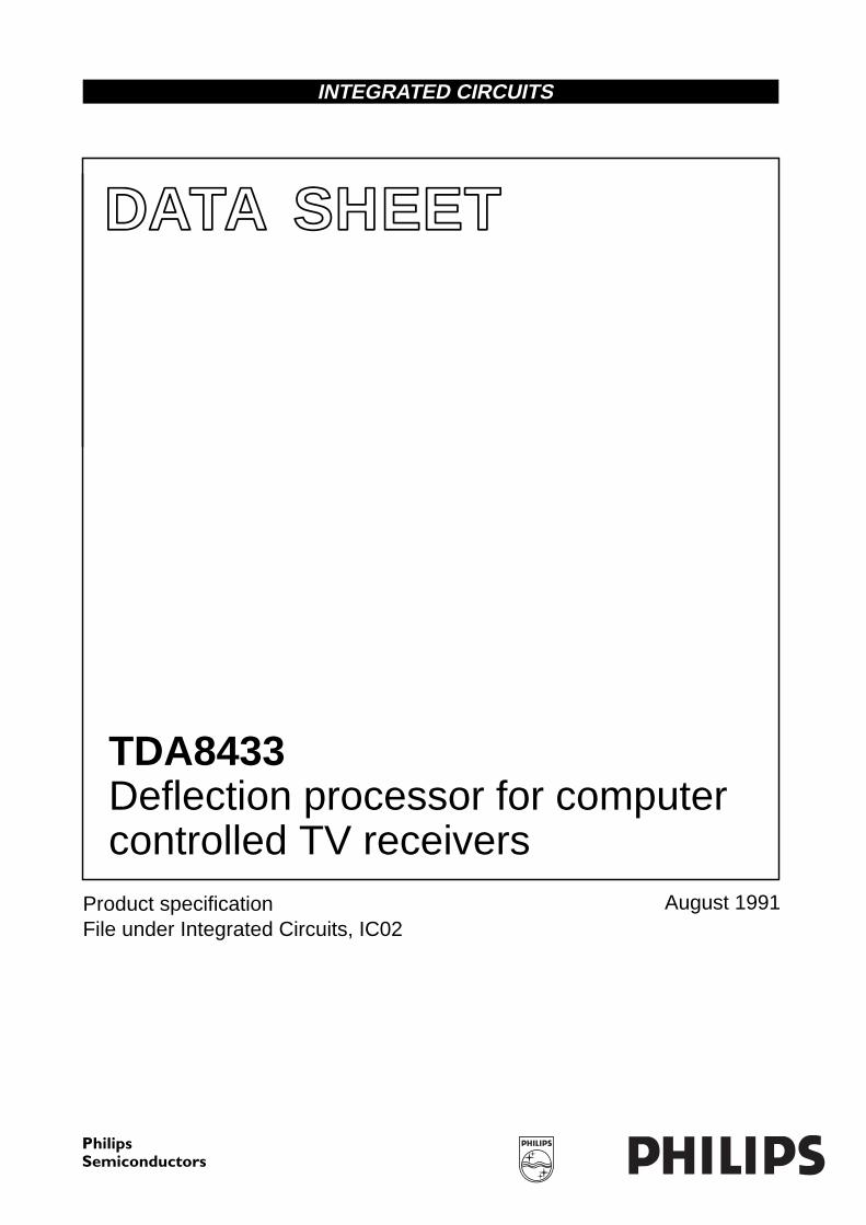
DATA SHEET
Product specificationFile under Integrated Circuits, IC02
August 1991
INTEGRATED CIRCUITS
TDA8433Deflection processor for computercontrolled TV receivers
August 1991 2
Philips Semiconductors Product specification
Deflection processor for computercontrolled TV receivers
TDA8433
FEATURES
• I2C-bus interface
• Input for vertical sync
• Sawtooth generator with amplitudeindependent of frequency
• Vertical deflection output stagedriver
• East-west raster correction driveoutput
• EHT modulation input
• Changes picture width and heightwithout affecting geometry.
GENERAL DESCRIPTION
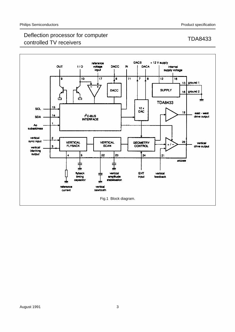
The TDA8433 is an I2C-buscontrolled deflection processor which,together with a sync processor (e.g.TDA2579A, see Fig.6), contains thecontrol and drive functions of thedeflection part in a computercontrolled TV receiver. The TDA8433replaces all picture geometry settingswhich were previously set manuallyduring manufacture.
QUICK REFERENCE DATA
Note to quick reference data
1. VRin = 0; V-S-corr = 0; Vshift = 20 H; Vampl = 20 H.
ORDERING INFORMATION
Note
1. SOT101-1; 1996 December 2.
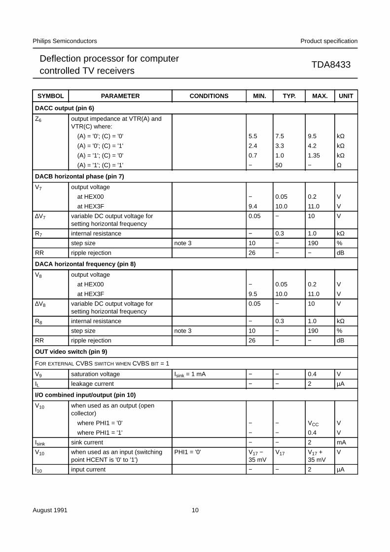
SYMBOL PARAMETER MIN. TYP. MAX. UNIT
VCC supply voltage (pin 12) 10.8 12.0 13.2 V
ICC supply current (pin 12) 12 20 27 mA
V2 vertical sync trigger level − 3 − V
V21 vertical feedback (note 1)
DC level −1.7 1.85 2.05 V
AC level 1.65 1.8 1.95 VP
V24 EHT compensation operating range 1.7 − 6 V
V11-13 inputs for control register data:
not locked to video − 0.7 1 V
at 50 Hz status 0.8 VCC − − V
at 60 Hz status − − 0.7 VCC V
V10-13 HCENT comparator switching level − V17 − V
V14-13 SDA I2C-bus switching level data input − 3.5 − V
V15 SCL I2C-bus switching level clock input − 3.5 − V
V1 device selection where:
Ao = '1' 9.0 − VCC V
Ao = '0' 0 − 2.0 V
EXTENDED TYPE NUMBERPACKAGE
PINS PIN POSITION MATERIAL CODE
TDA8433 24 DIL plastic SOT101(1)
August 1991 3
Philips Semiconductors Product specification
Deflection processor for computercontrolled TV receivers
TDA8433
Fig.1 Block diagram.
August 1991 4
Philips Semiconductors Product specification
Deflection processor for computercontrolled TV receivers
TDA8433
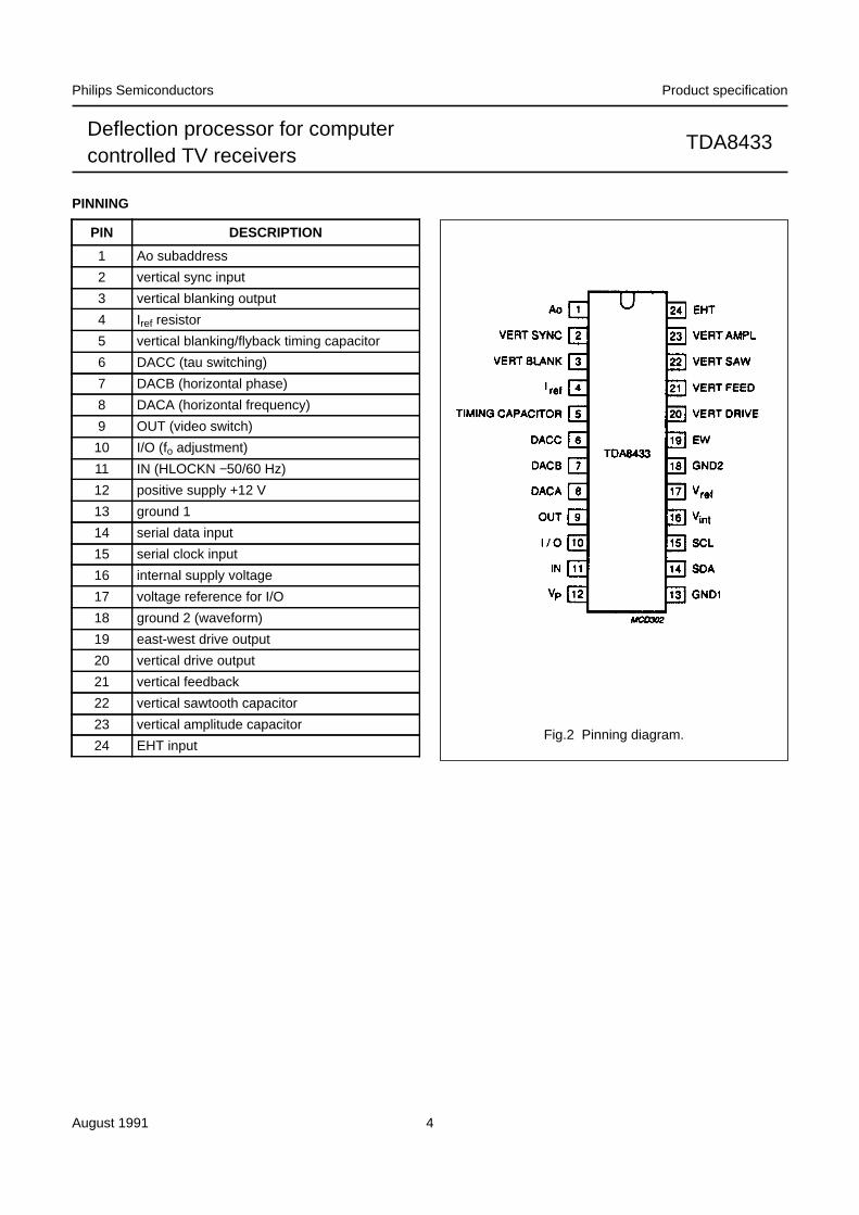
PINNING
PIN DESCRIPTION
1 Ao subaddress
2 vertical sync input
3 vertical blanking output
4 Iref resistor
5 vertical blanking/flyback timing capacitor
6 DACC (tau switching)
7 DACB (horizontal phase)
8 DACA (horizontal frequency)
9 OUT (video switch)
10 I/O (fo adjustment)
11 IN (HLOCKN −50/60 Hz)
12 positive supply +12 V
13 ground 1
14 serial data input
15 serial clock input
16 internal supply voltage
17 voltage reference for I/O
18 ground 2 (waveform)
19 east-west drive output
20 vertical drive output
21 vertical feedback
22 vertical sawtooth capacitor
23 vertical amplitude capacitor
24 EHT inputFig.2 Pinning diagram.
August 1991 5
Philips Semiconductors Product specification
Deflection processor for computercontrolled TV receivers
TDA8433
PIN FUNCTIONS
Pin 1 - Ao subaddress
The Ao bit is the least significant bitof the bus-address. It enables twoTDA8433s, with differentaddresses, to be connected to thesame bus.
Pin 2 - Vertical sync input
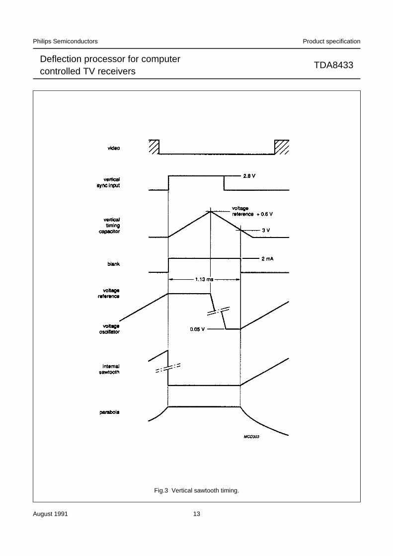
Positive trigger pulses of > 3 V aresufficient to exceed the internalthreshold of the ramp generator.Flyback and blanking will then startand, during the blanking period, thecircuit will be inhibited for furtherinput pulses (see Fig.3). It should benoted that the TDA8433 has novertical oscillator therefore, the syncprocessor, which is used in thiscombination, has to provide triggerpulses as well when the video inputis absent.
Pin 3 - Vertical blanking
The positive going blanking pulse isfed from a current source. Theblanking period is fixed by thecapacitor connected to pin 5 and theresistor connected to pin 4 (seeFig.3).
Pins 4 and 5 - Reference/flybacktiming
The external resistor connectedbetween pin 4 and ground providesa reference current for the trianglegenerator circuit. This circuitgenerates the triangle waveform atpin 5. The width of the blankingpulse is set by the externalcapacitor connected to pin 5.
Table 1 Sync processor time constants
VTRA VTRC OUTPUT TIME CONSTANT
'0' '0' 12 V automatic operation
'0' '1' 5.3 V medium
'1' '0' 1.5 V fast (video recorder)
'1' '1' 0.2 V not to be used
Pin 6 - DACC (tau switching)
The output voltage, which dependson the VTRA and VTRC bits in theI2C-bus control register, is connectedto the coincidence detector of thesync processor. In this way the timeconstants of the horizontal PLL (in thesync processor) can be set. If theTDA2579 is used (see Fig.6) theeffect will be as listed in Table 1.
Pin 7 - DACB (horizontal phase)
The voltage at pin 7 is fed to thehorizontal pulse modulator in the syncprocessor. This voltage, together withthe signal produced by the phase 2detector during horizontal flyback,sets the phase of the horizontaloutput with respect to the flybackpulse in the horizontal output stage.The voltage range is variablebetween 0.05 V and 10 V.
Pin 8 - DACA (horizontalfrequency)
The frequency of the horizontaloscillator in the external syncprocessor is adjusted by the voltagelevel at pin 8. The voltage is variablein 63 steps from 0.05 V to 10 V (i.e.0.158 V per step).
Pin 9 - OUT (video switch)
The output at pin 9 is controlled by theCVBS bit from the control registerwhere
CVBS = logic 0; the output is HIGH(open collector)
CVBS = logic 1; the output is LOW(saturation voltage)
An external video selector can becontrolled by means of this switchingfunction.
Pins 10 and 17 - I/O and Voltagereference
Pin 10 is connected to the output ofthe phase 1 detector in the syncprocessor. Whether the pin is used asan input or an output is dependent onthe PHI1 bit of the horizontalfrequency (HFREQ) register. WhenPHI = logic 0 (output transistor open)pin 10 is used as an input. The DCinformation at this pin is comparedwith the reference voltage at pin 17and is reflected in the HCENT of thestatus register.
HCENT = logic 0; input > Vref at V17
HCENT = logic 1; input < Vref at V17
In this way the free running frequencycan be adjusted by computer whilethe oscillator is locked. Alternatively,when PHI1 = logic 1, pin 10 isswitched to ground. The free runningfrequency of the oscillator can the beadjusted while watching the screenprovided that pin 10 is connected tothe video input of the sync processor.
Pin 11 -IN (HLOCKN and 50/60 Hz)
This pin is connected to the combinedMUTE and 50/60 Hz pin of the syncprocessor. The various DC levelsdefine the state of the HLOCKN and50/60 Hz bits in the status register(see Table 2.)
August 1991 6
Philips Semiconductors Product specification
Deflection processor for computercontrolled TV receivers
TDA8433
Table 2 Status register bits
STATE OF SYNC PROCESSOR(TDA2579)
TYPICAL VOLTAGE AT PIN 11STATE OF
HLOCKN 50/60 Hz
Not locked to computer video < 0.7 V(min.) '1' '0'
60 Hz transmitter found 0.7 to 0.75 VCC '0' '0'
50 Hz transmitter found > 0.75 VCC to VCC '0' '1'
Pin 12 - Positive supply (12 V)
The nominal supply voltage at pin 12is 12 V which should remain withinthe defined limits. The nominalcurrent consumption is 20 mA.
Pins 13 and 18 - Ground (1 and 2)
Ground 1 (pin 13) is for the bustransceiver sectionGround 2 (pin 18) is for the sawtoothand picture geometry control section.
Pins 14 and 15 - SDA and SCL(serial data and serial clock)
Input serial data is applied to pin 14.The serial clock input from theI2C-bus is applied to pin 15.
Pin 16 - Internal supply voltage(+5 V)
In some applications it may benecessary to connect a capacitor tothis pin to avoid interference.
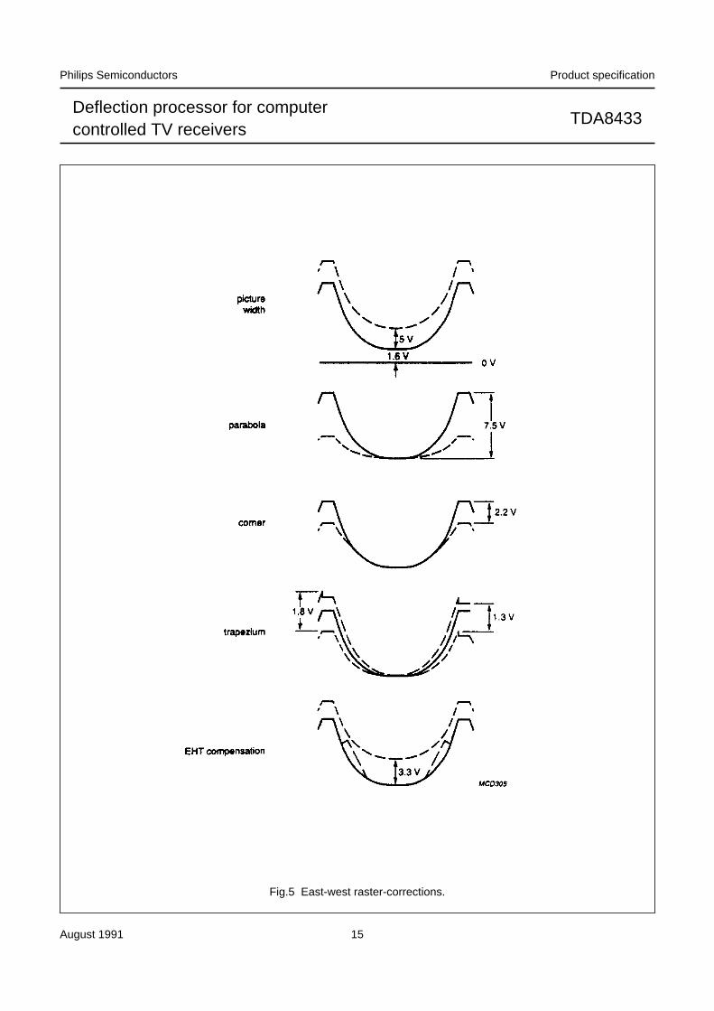
Pin 19 - East-west drive output
The output drive for the East-westcorrection circuit has a nominal rangefrom 1.6 to 11.7 V and contains 5programmable parameters (seeFig.5). The parameters are:
• Picture width
• East-west raster correction
• East-west trapezium correction
• East-west corner correction
• Compensation for EHT variations
Pins 20 and 21 - Vertical driveoutput and vertical feedback input
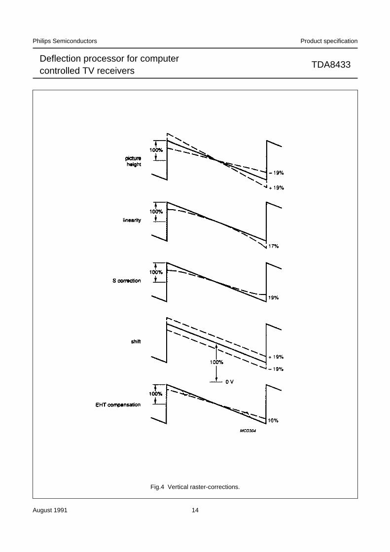
The vertical comparator and driveoutput stage is designed so that thefeedback signal applied to pin 21 canbe inverted in the comparator by theV-out control bit. This enables the useof two different vertical output stages.One output stage is without aninternal comparator (e.g. TDA3654).The feedback signal at pin 21 has anegative slope during scan. Duringpower-up the IC is adapted (preset)for this type of output stage. The otheroutput stage contains a comparator.The drive for this output stage isobtained by interconnecting pins 20and 21 and switching the V-outpolarity. The V-out bit will then be setto logic 1. In both cases the drivesignal available at pin 20 contains 5parameters which can be set via theI2C-bus control;
• Picture height
• Vertical linearity
• Vertical S-correction
• Vertical shift
• Extent of compensation for EHTvariations (see Fig.4.)
Pins 22 and 23 - Verticalsawtooth/vertical amplitudecapacitor
The 100 nF capacitor connected topin 22 is charged and discharged bytwo current sources in the verticalramp generator. In order to obtain an
equal amplitude, at differentfrequencies, an amplitudecomparator has been incorporated.The circuit, together with the 330 nFcapacitor connected to pin 23, keepsthe sawtooth amplitude at referencevoltage level (7.1 V). The externalload of the amplitude stabilizationloop of pin 23 should be as low aspossible. The recommended value is≥ 500 MΩ.
Pin 24 - EHT input (Modulation)
A voltage between 1.7 and 6 V(depending on the EHT variations)applied to pin 24 will modulate theamplitude of the vertical drivesawtooth and the East-west driveoutput. In this way the effect of beamcurrent variations can be virtuallyeliminated.
I2C-BUS CONTROL
The addresses for the I2C-bus are100011Ao0 (write) and 100011Ao1(read). The inclusion of the Ao bitmakes it possible to control twodifferent deflection processors. Afterreceiving the address byte theI2C-bus transmits its status byte inwhich the status of the control bits iscontained.
PONRES - Power-on-reset
After switch-on, or a power dip below6.7 V, the PONRES bit is set to logic1. After a status read operationPONRES is reset to logic 0.
August 1991 7
Philips Semiconductors Product specification
Deflection processor for computercontrolled TV receivers
TDA8433
HLOCKN - Horizontal lock
This bit indicates whether thehorizontal oscillator in the syncprocessor is locked to the videosignal. When the oscillator is lockedHLOCKN is set to logic 0(V11 > 0.7 V). When the oscillator is
not locked HLOCKN is set to logic 1(V11 < 0.7 V).
HCENT - Horizontal centre
This bit is set to logic 0 when thehorizontal oscillator frequency is toohigh (V10 > Vref). The bit is set to logic
1 when the frequency is too lowV10 < Vref).
IN - 50/60 Hz
The voltage at pin 11 also containsthe 50/60 Hz information where:
logic 0 = ≤ V11 0.75 VCC (60 Hz or notransmitter)logic 1 = ≥ V11 0.75 VCC (50 Hz)
The sequence of data in the statusbyte is: PONRES, HLOCKN,50/60 Hz, 0 0 0 0.
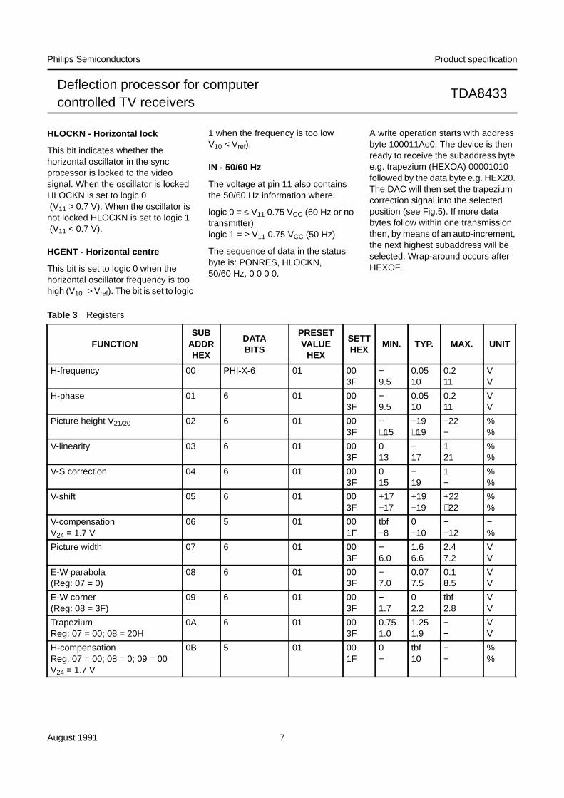
A write operation starts with addressbyte 100011Ao0. The device is thenready to receive the subaddress bytee.g. trapezium (HEXOA) 00001010followed by the data byte e.g. HEX20.The DAC will then set the trapeziumcorrection signal into the selectedposition (see Fig.5). If more databytes follow within one transmissionthen, by means of an auto-increment,the next highest subaddress will beselected. Wrap-around occurs afterHEXOF.
Table 3 Registers
FUNCTIONSUB
ADDRHEX
DATABITS
PRESETVALUE
HEX
SETTHEX
MIN. TYP. MAX. UNIT
H-frequency 00 PHI-X-6 01 003F
−9.5
0.0510
0.211
VV
H-phase 01 6 01 003F
−9.5
0.0510
0.211
VV
Picture height V21/20 02 6 01 003F
−+15
−19+19
−22−
%%
V-linearity 03 6 01 003F
013
−17
121
%%
V-S correction 04 6 01 003F
015
−19
1−
%%
V-shift 05 6 01 003F
+17−17
+19−19
+22+22
%%
V-compensationV24 = 1.7 V
06 5 01 001F
tbf−8
0−10
−−12
−%
Picture width 07 6 01 003F
−6.0
1.66.6
2.47.2
VV
E-W parabola(Reg: 07 = 0)
08 6 01 003F
−7.0
0.077.5
0.18.5
VV
E-W corner(Reg: 08 = 3F)
09 6 01 003F
−1.7
02.2
tbf2.8
VV
TrapeziumReg: 07 = 00; 08 = 20H
0A 6 01 003F
0.751.0
1.251.9
−−
VV
H-compensationReg. 07 = 00; 08 = 0; 09 = 00V24 = 1.7 V
0B 5 01 001F
0−
tbf10
−−
%%
August 1991 8
Philips Semiconductors Product specification
Deflection processor for computercontrolled TV receivers
TDA8433
Note to Table 3
1. tbf = value to be fixed.
LIMITING VALUESIn accordance with the Absolute Maximum System (IEC 134)
THERMAL RESISTANCE
Not used 0C/0E − − − − − −Control 0F X-VOUT − 40 11.5 11.9 VCC V
VTRA−VTRC − 50 5.0 5.3 5.6 V
CVBS−X−X−X − 60 1.2 1.5 1.8 V
70 0 0.2 0.5 V
40 5.5 7.5 9.5 kΩ50 2.4 3.3 4.2 kΩ60 0.7 1.0 1.35 kΩ70 − 50 − Ω00 − − (VBS) V
08 − − 0.4(1 mA)
V
PHI1 bit 00 1 − 80 − − 0.4(−2 mA)
V
00 − − VCC V
Not used 10−EF
Test functions F0−FF
SYMBOL PARAMETER MIN. MAX. UNIT
VCC supply voltage 10.8 13.2 V
ICC supply current 12 27 mA
Ptot total power dissipation − 360 mW
Tamb operating ambient temperature range −25 +75 °CTstg storage temperature range −55 +150 °C
SYMBOL PARAMETER TYP. MAX. UNIT
Rth j-a from junction to ambient in free air − 35 K/W
FUNCTIONSUB
ADDRHEX
DATABITS
PRESETVALUE
HEX
SETTHEX
MIN. TYP. MAX. UNIT
August 1991 9
Philips Semiconductors Product specification
Deflection processor for computercontrolled TV receivers
TDA8433
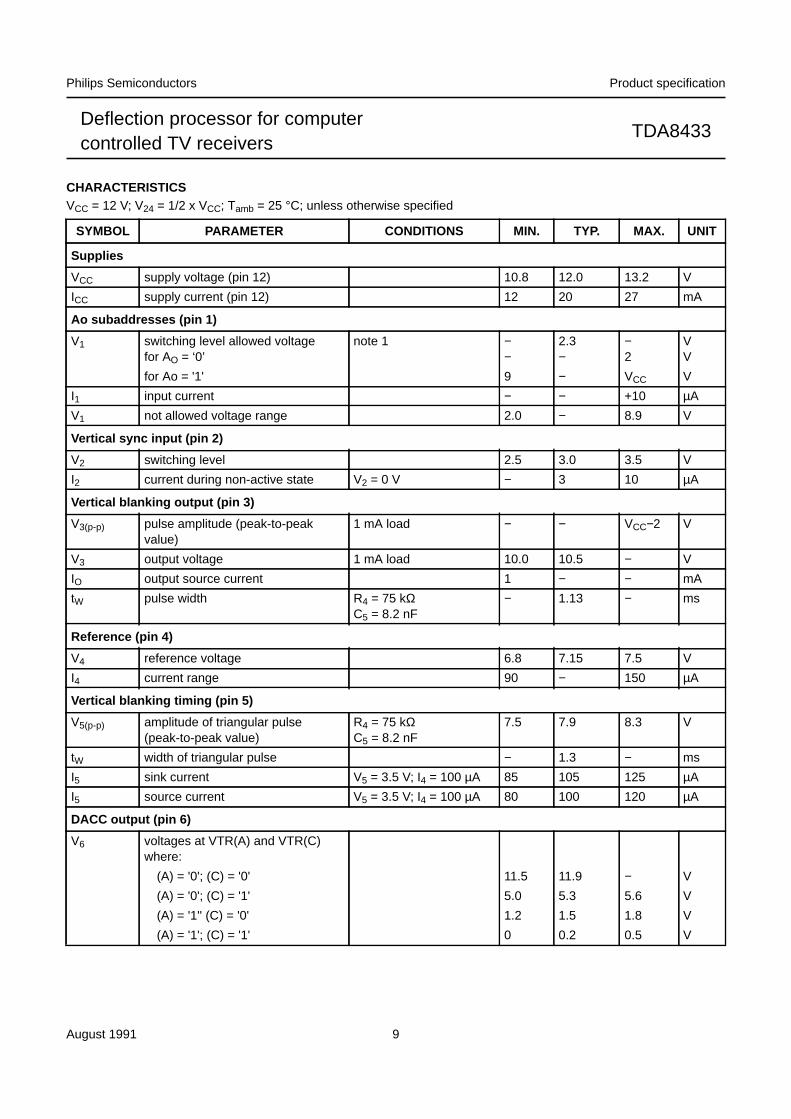
CHARACTERISTICSVCC = 12 V; V24 = 1/2 x VCC; Tamb = 25 °C; unless otherwise specified
SYMBOL PARAMETER CONDITIONS MIN. TYP. MAX. UNIT
Supplies
VCC supply voltage (pin 12) 10.8 12.0 13.2 V
ICC supply current (pin 12) 12 20 27 mA
Ao subaddresses (pin 1)
V1 switching level allowed voltagefor AO = ‘0’
note 1 −−
2.3−
−2
VV
for Ao = '1' 9 − VCC V
I1 input current − − +10 µA
V1 not allowed voltage range 2.0 − 8.9 V
Vertical sync input (pin 2)
V2 switching level 2.5 3.0 3.5 V
I2 current during non-active state V2 = 0 V − 3 10 µA
Vertical blanking output (pin 3)
V3(p-p) pulse amplitude (peak-to-peakvalue)
1 mA load − − VCC−2 V
V3 output voltage 1 mA load 10.0 10.5 − V
IO output source current 1 − − mA
tW pulse width R4 = 75 kΩC5 = 8.2 nF
− 1.13 − ms
Reference (pin 4)
V4 reference voltage 6.8 7.15 7.5 V
I4 current range 90 − 150 µA
Vertical blanking timing (pin 5)
V5(p-p) amplitude of triangular pulse(peak-to-peak value)
R4 = 75 kΩC5 = 8.2 nF
7.5 7.9 8.3 V
tW width of triangular pulse − 1.3 − ms
I5 sink current V5 = 3.5 V; I4 = 100 µA 85 105 125 µA
I5 source current V5 = 3.5 V; I4 = 100 µA 80 100 120 µA
DACC output (pin 6)
V6 voltages at VTR(A) and VTR(C)where:
(A) = '0'; (C) = '0' 11.5 11.9 − V
(A) = '0'; (C) = '1' 5.0 5.3 5.6 V
(A) = '1'' (C) = '0' 1.2 1.5 1.8 V
(A) = '1'; (C) = '1' 0 0.2 0.5 V
August 1991 10
Philips Semiconductors Product specification
Deflection processor for computercontrolled TV receivers
TDA8433
DACC output (pin 6)
Z6 output impedance at VTR(A) andVTR(C) where:
(A) = '0'; (C) = '0' 5.5 7.5 9.5 kΩ(A) = '0'; (C) = '1' 2.4 3.3 4.2 kΩ(A) = '1'; (C) = '0' 0.7 1.0 1.35 kΩ(A) = '1'; (C) = '1' − 50 − Ω
DACB horizontal phase (pin 7)
V7 output voltage
at HEX00 − 0.05 0.2 V
at HEX3F 9.4 10.0 11.0 V
∆V7 variable DC output voltage forsetting horizontal frequency
0.05 − 10 V
R7 internal resistance − 0.3 1.0 kΩstep size note 3 10 − 190 %
RR ripple rejection 26 − − dB
DACA horizontal frequency (pin 8)
V8 output voltage
at HEX00 − 0.05 0.2 V
at HEX3F 9.5 10.0 11.0 V
∆V8 variable DC output voltage forsetting horizontal frequency
0.05 − 10 V
R8 internal resistance − 0.3 1.0 kΩstep size note 3 10 − 190 %
RR ripple rejection 26 − − dB
OUT video switch (pin 9)
FOR EXTERNAL CVBS SWITCH WHEN CVBS BIT = 1
V9 saturation voltage Isink = 1 mA − − 0.4 V
IL leakage current − − 2 µA
I/O combined input/output (pin 10)
V10 when used as an output (opencollector)
where PHI1 = '0' − − VCC V
where PHI1 = '1' − − 0.4 V
Isink sink current − − 2 mA
V10 when used as an input (switchingpoint HCENT is '0' to '1')
PHI1 = '0' V17 −35 mV
V17 V17 +35 mV
V
I10 input current − − 2 µA
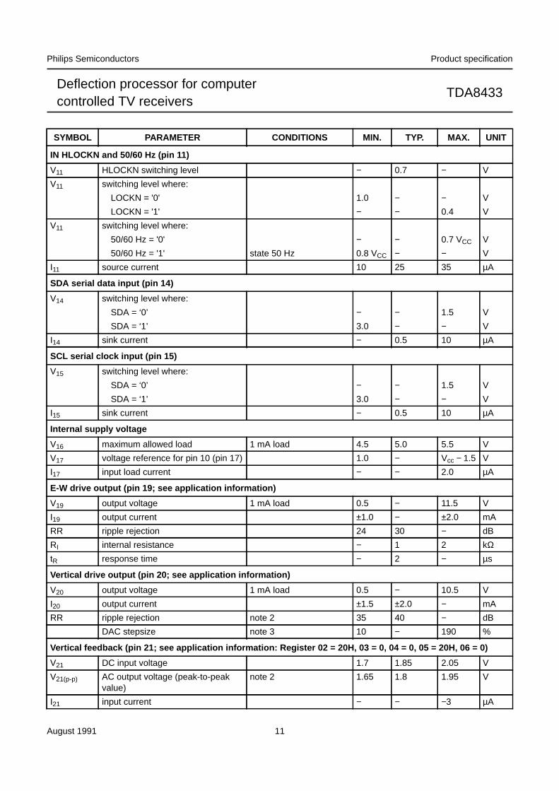
SYMBOL PARAMETER CONDITIONS MIN. TYP. MAX. UNIT
August 1991 11
Philips Semiconductors Product specification
Deflection processor for computercontrolled TV receivers
TDA8433
IN HLOCKN and 50/60 Hz (pin 11)
V11 HLOCKN switching level − 0.7 − V
V11 switching level where:
LOCKN = '0' 1.0 − − V
LOCKN = '1' − − 0.4 V
V11 switching level where:
50/60 Hz = '0' − − 0.7 VCC V
50/60 Hz = '1' state 50 Hz 0.8 VCC − − V
I11 source current 10 25 35 µA
SDA serial data input (pin 14)
V14 switching level where:
SDA = ‘0’ − − 1.5 V
SDA = ‘1’ 3.0 − − V
I14 sink current − 0.5 10 µA
SCL serial clock input (pin 15)
V15 switching level where:
SDA = ‘0’ − − 1.5 V
SDA = ‘1’ 3.0 − − V
I15 sink current − 0.5 10 µA
Internal supply voltage
V16 maximum allowed load 1 mA load 4.5 5.0 5.5 V
V17 voltage reference for pin 10 (pin 17) 1.0 − Vcc − 1.5 V
I17 input load current − − 2.0 µA
E-W drive output (pin 19; see application information)
V19 output voltage 1 mA load 0.5 − 11.5 V
I19 output current ±1.0 − ±2.0 mA
RR ripple rejection 24 30 − dB
RI internal resistance − 1 2 kΩtR response time − 2 − µs
Vertical drive output (pin 20; see application information)
V20 output voltage 1 mA load 0.5 − 10.5 V
I20 output current ±1.5 ±2.0 − mA
RR ripple rejection note 2 35 40 − dB
DAC stepsize note 3 10 − 190 %
Vertical feedback (pin 21; see application information: Register 02 = 20H, 03 = 0, 04 = 0, 05 = 20H, 06 = 0)
V21 DC input voltage 1.7 1.85 2.05 V
V21(p-p) AC output voltage (peak-to-peakvalue)
note 2 1.65 1.8 1.95 V
I21 input current − − −3 µA
SYMBOL PARAMETER CONDITIONS MIN. TYP. MAX. UNIT
August 1991 12
Philips Semiconductors Product specification
Deflection processor for computercontrolled TV receivers
TDA8433
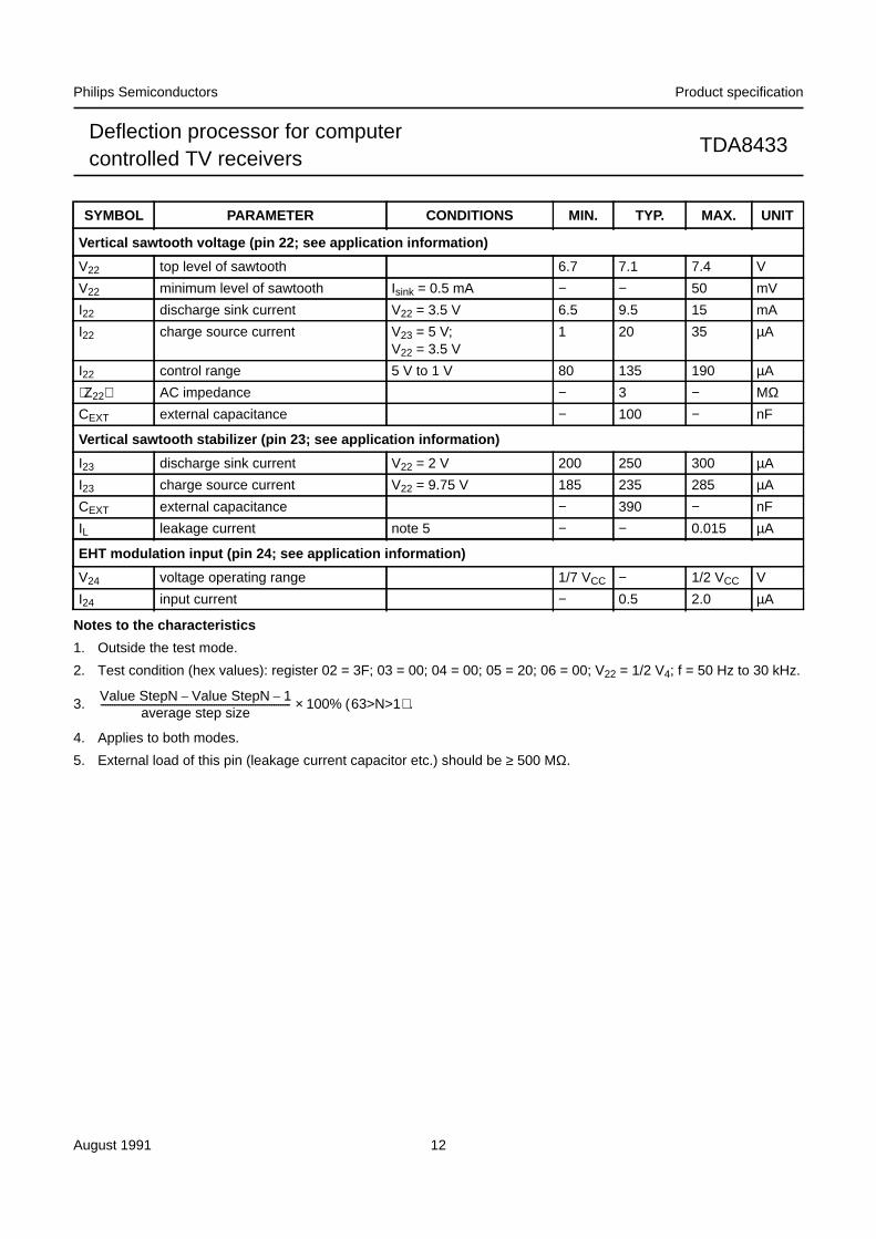
Notes to the characteristics
1. Outside the test mode.
2. Test condition (hex values): register 02 = 3F; 03 = 00; 04 = 00; 05 = 20; 06 = 00; V22 = 1/2 V4; f = 50 Hz to 30 kHz.
3.
4. Applies to both modes.
5. External load of this pin (leakage current capacitor etc.) should be ≥ 500 MΩ.
Vertical sawtooth voltage (pin 22; see application information)
V22 top level of sawtooth 6.7 7.1 7.4 V
V22 minimum level of sawtooth Isink = 0.5 mA − − 50 mV
I22 discharge sink current V22 = 3.5 V 6.5 9.5 15 mA
I22 charge source current V23 = 5 V;V22 = 3.5 V
1 20 35 µA
I22 control range 5 V to 1 V 80 135 190 µA
Z22 AC impedance − 3 − MΩCEXT external capacitance − 100 − nF
Vertical sawtooth stabilizer (pin 23; see application information)
I23 discharge sink current V22 = 2 V 200 250 300 µA
I23 charge source current V22 = 9.75 V 185 235 285 µA
CEXT external capacitance − 390 − nF
IL leakage current note 5 − − 0.015 µA
EHT modulation input (pin 24; see application information)
V24 voltage operating range 1/7 VCC − 1/2 VCC V
I24 input current − 0.5 2.0 µA
SYMBOL PARAMETER CONDITIONS MIN. TYP. MAX. UNIT
Value StepN Value StepN– 1–average step size
---------------------------------------------------------------------------------- 100% 63>N>1( ) .×
August 1991 13
Philips Semiconductors Product specification
Deflection processor for computercontrolled TV receivers
TDA8433
Fig.3 Vertical sawtooth timing.
August 1991 14
Philips Semiconductors Product specification
Deflection processor for computercontrolled TV receivers
TDA8433
Fig.4 Vertical raster-corrections.
August 1991 15
Philips Semiconductors Product specification
Deflection processor for computercontrolled TV receivers
TDA8433
Fig.5 East-west raster-corrections.
August 1991 16
Philips Semiconductors Product specification
Deflection processor for computercontrolled TV receivers
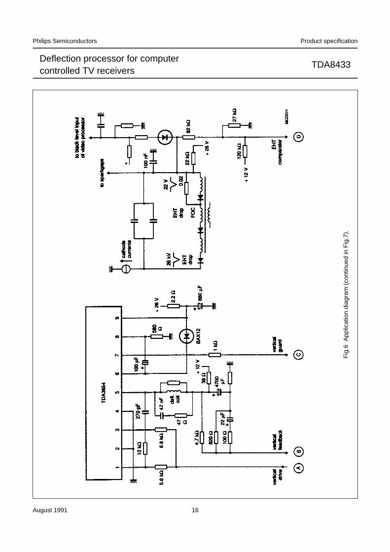
TDA8433
Fig
.6 A
pplic
atio
n di
agra
m (
cont
inue
d in
Fig
.7).
August 1991 17
Philips Semiconductors Product specification
Deflection processor for computercontrolled TV receivers
TDA8433
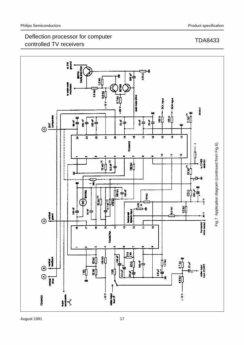
Fig
.7 A
pplic
atio
n di
agra
m (
cont
inue
d fr
om F
ig.6
).
August 1991 18
Philips Semiconductors Product specification
Deflection processor for computercontrolled TV receivers
TDA8433
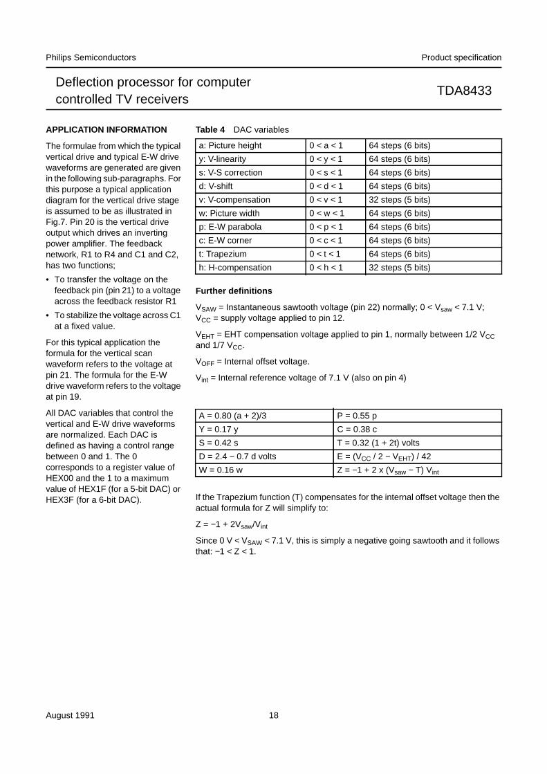
APPLICATION INFORMATION
The formulae from which the typicalvertical drive and typical E-W drivewaveforms are generated are givenin the following sub-paragraphs. Forthis purpose a typical applicationdiagram for the vertical drive stageis assumed to be as illustrated inFig.7. Pin 20 is the vertical driveoutput which drives an invertingpower amplifier. The feedbacknetwork, R1 to R4 and C1 and C2,has two functions;
• To transfer the voltage on thefeedback pin (pin 21) to a voltageacross the feedback resistor R1
• To stabilize the voltage across C1at a fixed value.
For this typical application theformula for the vertical scanwaveform refers to the voltage atpin 21. The formula for the E-Wdrive waveform refers to the voltageat pin 19.
All DAC variables that control thevertical and E-W drive waveformsare normalized. Each DAC isdefined as having a control rangebetween 0 and 1. The 0corresponds to a register value ofHEX00 and the 1 to a maximumvalue of HEX1F (for a 5-bit DAC) orHEX3F (for a 6-bit DAC).
Table 4 DAC variables
Further definitions
VSAW = Instantaneous sawtooth voltage (pin 22) normally; 0 < Vsaw < 7.1 V;VCC = supply voltage applied to pin 12.
VEHT = EHT compensation voltage applied to pin 1, normally between 1/2 VCCand 1/7 VCC.
VOFF = Internal offset voltage.
Vint = Internal reference voltage of 7.1 V (also on pin 4)
If the Trapezium function (T) compensates for the internal offset voltage then theactual formula for Z will simplify to:
Z = −1 + 2Vsaw/Vint
Since 0 V < VSAW < 7.1 V, this is simply a negative going sawtooth and it followsthat: −1 < Z < 1.
a: Picture height 0 < a < 1 64 steps (6 bits)
y: V-linearity 0 < y < 1 64 steps (6 bits)
s: V-S correction 0 < s < 1 64 steps (6 bits)
d: V-shift 0 < d < 1 64 steps (6 bits)
v: V-compensation 0 < v < 1 32 steps (5 bits)
w: Picture width 0 < w < 1 64 steps (6 bits)
p: E-W parabola 0 < p < 1 64 steps (6 bits)
c: E-W corner 0 < c < 1 64 steps (6 bits)
t: Trapezium 0 < t < 1 64 steps (6 bits)
h: H-compensation 0 < h < 1 32 steps (5 bits)
A = 0.80 (a + 2)/3 P = 0.55 p
Y = 0.17 y C = 0.38 c
S = 0.42 s T = 0.32 (1 + 2t) volts
D = 2.4 − 0.7 d volts E = (VCC / 2 − VEHT) / 42
W = 0.16 w Z = −1 + 2 x (Vsaw − T) Vint
August 1991 19
Philips Semiconductors Product specification
Deflection processor for computercontrolled TV receivers
TDA8433
Vertical drive waveform
The vertical drive waveform hascertain interactions between theparameters whereby:
• The S-correction influences thepicture height
• The linearity correction caninfluence the picture shift.
The alignment can be madenon-repetitive. Once correct valuesfor the V-S correction and V-linearityare set, the picture height may bechanged without affecting the V-Scorrection and V-linearity on thescreen.
The formula for the vertical drivewaveform at pin 21 is:
Vvert = D + 1.32 A (Z − SA2 Z3)(1 − VE) + YZ2 volts.
Picture height
The amplitude of the sawtoothwaveform is controlled by 'A'. Itfollows therefore that:
0.53 < A < 0.8
The nominal value for 'A' is found fora = 0.5, therefore A = 0.67. Byprogramming the picture height, thesawtooth amplitude can be adjustedfrom −19% to +19%. WithoutS-correction (S = O) and linearitycorrection (Y = O), the nominalsawtooth amplitude is (with A = 0.67);
1.32 x 0.67 x 2 = 1.77 V(p-p)
V-linearity
This function is meant to compensatefor non-linearity of AC coupledvertical output stages. The linearitycorrection changes proportionally tothe picture height setting. The rangefor linearity control is typically 17% of
the peak-to-peak value of the linearsawtooth (see Fig.7).
V-S correction
The range for the V-S correction(SA2) is defined as a percentage ofthe undistorted peak-to-peaksawtooth voltage (see Fig.7). Theactual S-correction component (SA2)is dependent on the picture heightsetting where:
At maximum picture height (A = 0.80): SA2 = 0.282At nominal picture height (A = 0.62) :SA2 = 0.197At minimum picture height (A = 0.53): SA2 = 0.125
Picture shift
The DC level of the output is fixed by'D'. It can be adjusted within a rangeof −19% to +19%. In actualapplication this will be used forshifting the picture vertically.
V-compensation
The vertical deflection can bemodulated by the instantaneousvalue of the signal applied to the EHTcompensation input. This externalsignal should reflect the EHTvariations. The amount of deflectionreduction is in the range 0 to 10%, ifpin 24 is at (VCC / 2) − 4.3 V(maximum modulation i.e. 1.7 Vtypical). Thus for maximummodulation, the V-drive waveformcan be reduced to 90% of its value.There is no reduction when theEHT-compensation input is atVCC / 2 V (i.e. 6 V typical).
Trapezium
The trapezium function is the onlyIC-confined adjustment and isintended to compensate for anyinternal offsets. The function is calledTrapezium because of its effect onthe picture if an AC-coupled verticaldeflection stage is used. Thetrapezium function can alter thepicture shift range by a maximum of190 mV. If the trapezium function isused for purposes other thaneliminating the internal offsets, thenthe V-linearity can affect the actualpicture height. This can affect thesymmetry of the S-correction which,in turn, can affect the V-linearity.
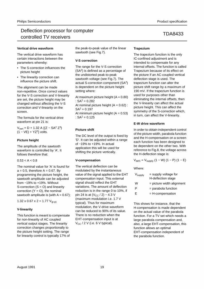
E-W drive waveform
In order to obtain independent controlof the picture width, parabola functionand the H-compensation on a screeneach function has been designed tobe dependent on the other two. Withreference to Fig.8, the voltage acrossthe H-deflection stage is:
Vdef1 = Vsupply (1 − W) (1 − P) (1 − E)
Where:
This shows for instance, that theH-compensation is made dependenton the actual value of the parabolafunction. For a TV set which needs alarge parabola compensation and,also, a large EHT-compensation, thisfunction allows an optimalEHT-compensation independent ofthe parabola function.
Vsupply = supply voltage forH-deflection stage
W = picture width alignment
P = parabola function
E = H-compensation
August 1991 20
Philips Semiconductors Product specification
Deflection processor for computercontrolled TV receivers
TDA8433
All correction voltages are related tothe supply voltage. The TDA8433 isdesigned to accept a supply voltageof 30 V. Normally higher voltages areemployed therefore a voltageamplifier, with a gain of Vsupply/30, isused between the TDA8433 and thediode modulator.
The formula for the E-W drive outputvoltage at pin 19 is:
VE-W = 30 x 1 − (1 − W) (1 − PA2 Z2 +CA4 Z4) (1 − 1.1 x hE) + 1.8 V
As can be seen from the formula, thepicture width, parabola function andH-compensation are influenced byeach other. The functions arediscussed separately with the othercompensations set to zero.
Picture width control (P-C-h-O)
It is possible to change the picturewidth by adjusting 'W' from 0 to 0.16.Thus the complete range for thepicture control width is −10 to +10%.By only changing the picture widthcontrol the output voltage at pin 19can vary between 1.8 and 6.6 Vtypical.
Parabola function
The parabola function is alsodependent on the picture heightfunction. The values given are validfor a nominal height setting(A = 0.67 V). The parabola functionconsists of two parts:
• A parabola part - E-W parabola iscreated by squaring a linearsawtooth. The range of this pureparabola varies from 0 to 25%typical i.e. the amplitude of theparabola waveform isprogrammable from 0 to 7.5 V(typical).
• A fourth order part - E-W corner iscreated by squaring the parabola.The range of this corner correctionvaries from 0 to 7% (typical) i.e. theamplitude of the corner correctionwaveform is programmable from 0to −2.2 V (typical). A negativeoutput voltage is not possible. TheE-W corner correction waveformhas to be subtracted from one ofthe other alignment functions.
The split-up into the E-W parabolaand the E-W corner enables eachtelevision set to be aligned withstraight vertical lines. The trapeziumis also related to the parabolafunction. The main reason for thetrapezium correction is tocompensate for internal offsets in thegeometry control part. Therefore:
• The amount of trapeziumcorrection is fully dependent on theamount of parabola correction andcorner correction that is needed.With no parabola and cornercorrection the trapezium output willbe zero.
• The maximum possible trapeziumoutput is 1.6 V (typical - see Fig.7).This is the case where: a = 0.5, c =0 and p = 1 i.e. no corner correctionand the maximum parabolacorrection at nominal picture heightsettings.
H-compensation control
The horizontal deflection can bemodulated by the instantaneousvalue of the signal applied to the EHTcompensation input. This externalsignal should reflect the EHTvariations. The amount of deflectionreduction is in the range 0 to 10% ifthe input at pin 7 is at(Vsupply/2) −4.3 V (maximummodulation is 1.7 V typical). Withmaximum modulation this rangecorresponds to an output voltage of0 to 3.3 V. There is no reduction whenthe EHT-compensation input is atVsupply/2 V (typical 6 V).
August 1991 21
Philips Semiconductors Product specification
Deflection processor for computercontrolled TV receivers
TDA8433
Fig.8 Application diagram of an AC coupled amplifier stage.
Fig.9 Application diagram for driving the diode modulator.
August 1991 22
Philips Semiconductors Product specification
Deflection processor for computercontrolled TV receivers
TDA8433
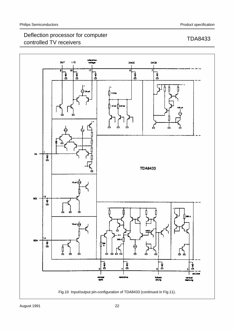
Fig.10 Input/output pin-configuration of TDA8433 (continued in Fig.11).
August 1991 23
Philips Semiconductors Product specification
Deflection processor for computercontrolled TV receivers
TDA8433
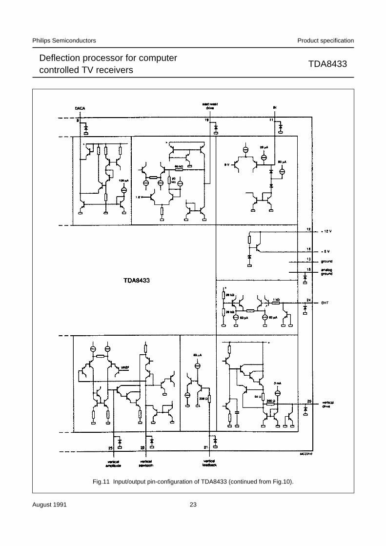
Fig.11 Input/output pin-configuration of TDA8433 (continued from Fig.10).
August 1991 24
Philips Semiconductors Product specification
Deflection processor for computercontrolled TV receivers
TDA8433
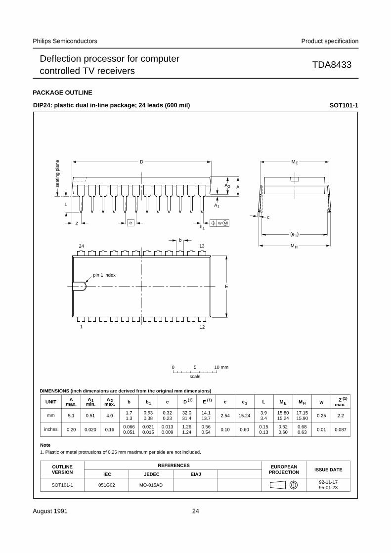
PACKAGE OUTLINE
UNIT Amax.
1 2 b1 c D E e MHL
REFERENCESOUTLINEVERSION
EUROPEANPROJECTION ISSUE DATE
IEC JEDEC EIAJ
mm
inches
DIMENSIONS (inch dimensions are derived from the original mm dimensions)
SOT101-192-11-1795-01-23
A min.
A max. b wMEe1
1.71.3
0.530.38
0.320.23
32.031.4
14.113.7
3.93.4 0.252.54 15.24
15.8015.24
17.1515.90 2.25.1 0.51 4.0
0.0660.051
0.0210.015
0.0130.009
1.261.24
0.560.54
0.150.13 0.010.10 0.60
0.620.60
0.680.63 0.0870.20 0.020 0.16
051G02 MO-015AD
MH
c
(e )1
ME
A
L
seat
ing
plan
e
A1
w Mb1
e
D
A2
Z
24
1
13
12
b
E
pin 1 index
0 5 10 mm
scale
Note
1. Plastic or metal protrusions of 0.25 mm maximum per side are not included.
Zmax.
(1)(1)(1)
DIP24: plastic dual in-line package; 24 leads (600 mil) SOT101-1
August 1991 25
Philips Semiconductors Product specification
Deflection processor for computercontrolled TV receivers
TDA8433
SOLDERING
Introduction
There is no soldering method that is ideal for all ICpackages. Wave soldering is often preferred whenthrough-hole and surface mounted components are mixedon one printed-circuit board. However, wave soldering isnot always suitable for surface mounted ICs, or forprinted-circuits with high population densities. In thesesituations reflow soldering is often used.
This text gives a very brief insight to a complex technology.A more in-depth account of soldering ICs can be found inour “IC Package Databook” (order code 9398 652 90011).
Soldering by dipping or by wave
The maximum permissible temperature of the solder is260 °C; solder at this temperature must not be in contact
with the joint for more than 5 seconds. The total contacttime of successive solder waves must not exceed5 seconds.
The device may be mounted up to the seating plane, butthe temperature of the plastic body must not exceed thespecified maximum storage temperature (Tstg max). If theprinted-circuit board has been pre-heated, forced coolingmay be necessary immediately after soldering to keep thetemperature within the permissible limit.
Repairing soldered joints
Apply a low voltage soldering iron (less than 24 V) to thelead(s) of the package, below the seating plane or notmore than 2 mm above it. If the temperature of thesoldering iron bit is less than 300 °C it may remain incontact for up to 10 seconds. If the bit temperature isbetween 300 and 400 °C, contact may be up to 5 seconds.
DEFINITIONS
LIFE SUPPORT APPLICATIONS
These products are not designed for use in life support appliances, devices, or systems where malfunction of theseproducts can reasonably be expected to result in personal injury. Philips customers using or selling these products foruse in such applications do so at their own risk and agree to fully indemnify Philips for any damages resulting from suchimproper use or sale.
PURCHASE OF PHILIPS I2C COMPONENTS
Data sheet status
Objective specification This data sheet contains target or goal specifications for product development.
Preliminary specification This data sheet contains preliminary data; supplementary data may be published later.
Product specification This data sheet contains final product specifications.
Limiting values
Limiting values given are in accordance with the Absolute Maximum Rating System (IEC 134). Stress above one ormore of the limiting values may cause permanent damage to the device. These are stress ratings only and operationof the device at these or at any other conditions above those given in the Characteristics sections of the specificationis not implied. Exposure to limiting values for extended periods may affect device reliability.
Application information
Where application information is given, it is advisory and does not form part of the specification.
Purchase of Philips I2C components conveys a license under the Philips’ I2C patent to use thecomponents in the I2C system provided the system conforms to the I2C specification defined byPhilips. This specification can be ordered using the code 9398 393 40011.