Embed Size (px)
Citation preview

14/Nov/2007
DISPLAY Elektronik GmbH
DEM 20485 SYH-LY
LCD MODULE
Product Specification Version:1.1.0

GENERAL SPECIFICATION
MODULE NO. :
DEM 20485 SYH-LY CUSTOMER P/N
VERSION NO. CHANGE DESCRIPTION DATE
0 ORIGINAL VERSION 29.10.2001
1.1.0 CHANGE IC 14.11.2007
PREPARED BY: OYQ DATE: 14.11.2007
APPROVED BY: MH DATE: 22.11.2008
DEM 20485 SYH-LY Product Specification
Version: 1.1.0 PAGE: 1
1. FUNCTIONS & FEATURES ----------------------------------------------------------------- 2
2. MECHANICAL SPECIFICATIONS -------------------------------------------------------- 2
3. EXTERNAL DIMENSIONS------------------------------------------------------------------ 3
4. BLOCK DIAGRAM -------------------------------------------------------------------------- 3
5. PIN ASSIGNMENT --------------------------------------------------------------------------- 4
6. PCB DRAWING AND APPLICATION ---------------------------------------------------- 5
7. BACKLIGHT ELECTRICAL/OPTICAL SPECIFICATIONS-------------------------- 6
8. DISPLAY DATA RAM (DDRAM)---------------------------------------------------------- 7
9. MAXIMUM ABSOLUTE POWER LIMIT ------------------------------------------------ 7
10. CONTROL AND DISPLAY COMMAND------------------------------------------------- 8
11. STANDARD CHARACTER PATTERN(ST7066U-0A)----------------------------- 9
12. ELECTRICAL CHARACTERISTICS ----------------------------------------------------- 10
13. LCD MODULES HANDLING PERCAUTIONS---------------------------------------- 12
14. OTHERS --------------------------------------------------------------------------------------- 12
CONTENTS

DEM 20485 SYH-LY Product Specification
Version: 1.1.0 PAGE: 2
1.FUNCTIONS & FEATURES
MODULE NAME LCD TYPE DEM 20485 SYH-LY STN Yellow Green Transflective Positive Mode
Viewing Direction : 6 o'clock Driving Scheme : 1/16 Duty Cycle, 1/5 Bias Power Supply Voltage : 5 Volt (typ.) VLCD (VDD-V0) :4.5 Volt (typ.) Backlight Color : LED, Lightbox, Yellow-Green Display contents : 20 x4 Characters (5 x 8 dots, Format: 208 Kinds) Internal Memory : CGROM (10,080 bits )
: CGRAM (64 x 8 bits ) : DDRAM (80 x 8 bits for Digits)
CGROM : CGROM of the ST7066-0A Interface : Easy Interface with a 4-bit or 8-bit MPU Operating Temperature : -20°C to +70°C Storage Temperature : -30°C to +80°C
2. MECHANICAL SPECIFICATIONS
Module Size : 98.00 x 60.00 x 14.50 mm Character Font : 5 x 8 dots Character Size : 4.75 x 2.95 mm Character Pitch : 5.35 x 3.55 mm Dot Size : 0.55 x 0.55 mm Dot Pitch : 0.60 x 0.60 mm Dot Gap : 0.05mm

DEM 20485 SYH-LY Product Specification
Version: 1.1.0 PAGE: 3
3. EXTERNAL DIMENSIONS ( unit: mm)
4. BLOCK DIAGRAM
DB0~DB7ER/W LCDRS Controller
LSIV0 ST7066VDD
VSS
AK
SEGMENTDRIVERST7063
Control signals
SE
G41
~SE
G12
0
COM1~COM16LCD PANEL
4line*20characters
BACKLIGHT
SEG1~SEG40
SE
G12
1~S
EG
200
SEGMENTDRIVERST7063
DEM 20485 SYH-LY Product Specification
Version: 1.1.0 PAGE: 4
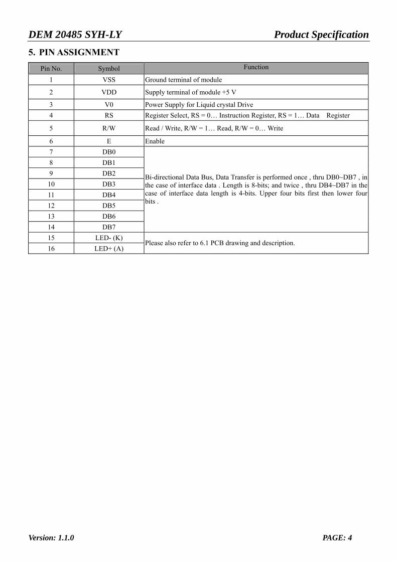
5. PIN ASSIGNMENT
Pin No. Symbol Function
1 VSS Ground terminal of module
2 VDD Supply terminal of module +5 V
3 V0 Power Supply for Liquid crystal Drive 4 RS Register Select, RS = 0… Instruction Register, RS = 1… Data Register
5 R/W Read / Write, R/W = 1… Read, R/W = 0… Write
6 E Enable 7 DB0 8 DB1 9 DB2
10 DB3 11 DB4 12 DB5 13 DB6 14 DB7
Bi-directional Data Bus, Data Transfer is performed once , thru DB0~DB7 , in the case of interface data . Length is 8-bits; and twice , thru DB4~DB7 in the case of interface data length is 4-bits. Upper four bits first then lower four bits .
15 LED- (K) 16 LED+ (A)
Please also refer to 6.1 PCB drawing and description.

DEM 20485 SYH-LY Product Specification
Version: 1.1.0 PAGE: 5
6. PCB DRAWING AND APPLICATION 6.1 PCB Drawing And Description
Note: on application module, R1~R5=820Ω, R6=91KΩ
Description : 6-1-1.The polarity of the pin 15 and the pin 16
LED Polarity J3,J5 J2, J4 15 Pin 16 Pin
Each open Each closed Anode Cathode
Each closed Each open Cathode Anode
Note: on application module, J3=J5= closed, J2=J4=open 6-1-2. The metal-bezel is set on ground when the J1 is closed .
Note: on application module, J1=closed
6-1-3.The LED resistor should can be bridged when the J6 is open.
Note: on application module, J6=open
6-1-4.The R7 and the R8 are the LED resistor.
Note: on application module, R7= R8=10Ω.
DEM 20485 SYH-LY Product Specification
Version: 1.1.0 PAGE: 6
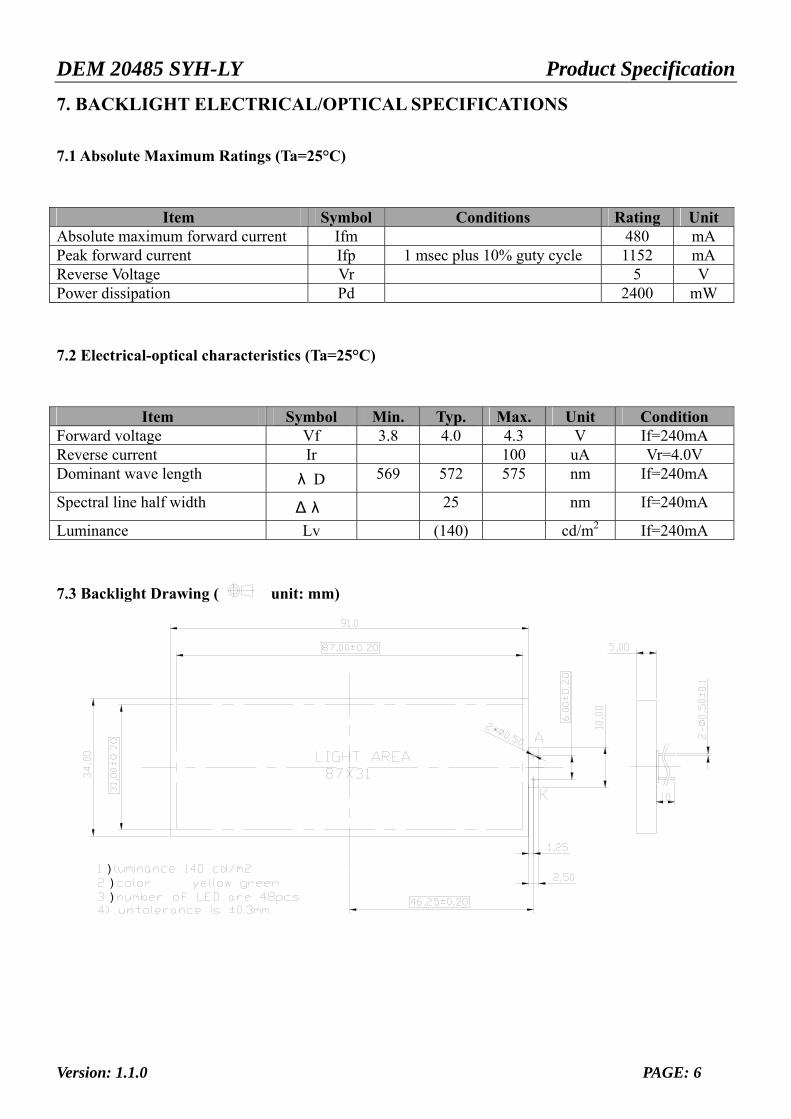
7. BACKLIGHT ELECTRICAL/OPTICAL SPECIFICATIONS
7.1 Absolute Maximum Ratings (Ta=25°C)
Item Symbol Conditions Rating Unit Absolute maximum forward current Ifm 480 mA Peak forward current Ifp 1 msec plus 10% guty cycle 1152 mA Reverse Voltage Vr 5 V Power dissipation Pd 2400 mW 7.2 Electrical-optical characteristics (Ta=25°C)
Item Symbol Min. Typ. Max. Unit Condition Forward voltage Vf 3.8 4.0 4.3 V If=240mA Reverse current Ir 100 uA Vr=4.0V Dominant wave length λ D 569 572 575 nm If=240mA
Spectral line half width Δ λ 25 nm If=240mA
Luminance Lv (140) cd/m2 If=240mA 7.3 Backlight Drawing ( unit: mm)
)))
DEM 20485 SYH-LY Product Specification
Version: 1.1.0 PAGE: 7
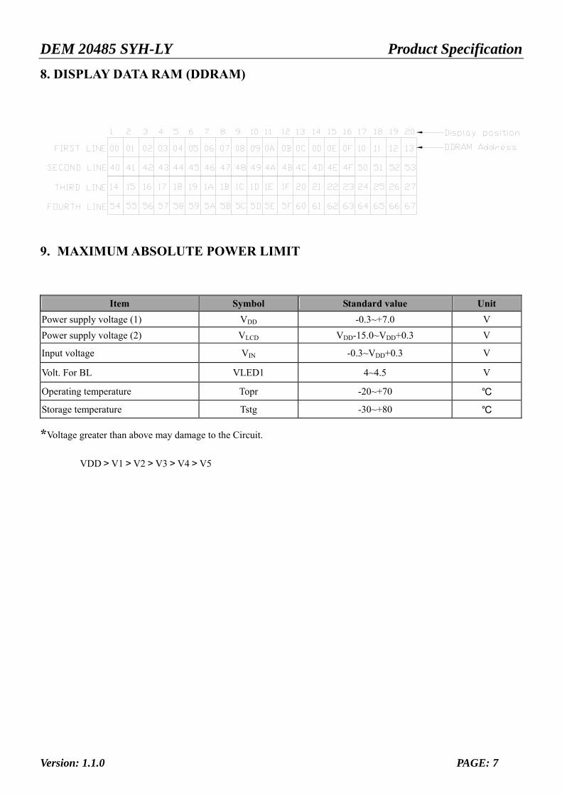
8. DISPLAY DATA RAM (DDRAM)
9. MAXIMUM ABSOLUTE POWER LIMIT
Item Symbol Standard value Unit Power supply voltage (1) VDD -0.3~+7.0 V Power supply voltage (2) VLCD VDD-15.0~VDD+0.3 V
Input voltage VIN -0.3~VDD+0.3 V
Volt. For BL VLED1 4~4.5 V
Operating temperature Topr -20~+70
Storage temperature Tstg -30~+80
*Voltage greater than above may damage to the Circuit.
VDD>V1>V2>V3>V4>V5

DEM 20485 SYH-LY Product Specification
Version: 1.1.0 PAGE: 8
10. CONTROL AND DISPLAY COMMAND
Command RS R/W DB7 DB6 DB5 DB4 DB3 DB2 DB1 DB0 Execution time (fosc=270KHz) Remark
Clear Display 0 0 0 0 0 0 0 0 0 1 1.52ms Write”20H” to DDRAM. And set
DDRAM address to “00H” from AC
Return home 0 0 0 0 0 0 0 0 1 x 1.52ms
Set DDRAM address to “00H” from AC and return cursor to its original position if shifted. The contents of DDRAM are not
changed.
Entry mode Set 0 0 0 0 0 0 0 1 I/D S 37us
Sets cursor move direction and specifies display shift. These operations are performed during data write and read.
Display on/off control
0 0 0 0 0 0 1 D C B 37us D=1: entire display on
C=1: cursor on B=1: cursor position on
Cursor or
Display Shift 0 0 0 0 0 1 S/C R/L x x 37us
Set cursor moving and display shift control bit, and the direction, without changing
DDRAM data.
function Set 0 0 0 0 1 DL N F x x 37us
DL: interface data is 8/4 bits N: number of line is 2/1 F: font size is 5x11/5x8
Set CGRAM address 0 0 0 1 AC5 AC4 AC3 AC2 AC1 AC0 37us Set CGRAM address in address counter
Set DDRAM address 0 0 1 AC6 AC5 AC4 AC3 AC2 AC1 AC0 37us Set DDRAM address in address counter
Read busy flag&
address 0 1 BF AC6 AC5 AC4 AC3 AC2 AC1 AC0 0us
Whether during internal operation or not can be known by reading BF. The contents
of address counter can also be read.
Write data to RAM 1 0 D7 D6 D5 D4 D3 D2 D1 D0 37us Write data into internal RAM
(DDRAM/CGRAM)
Read data from RAM 1 1 D7 D6 D5 D4 D3 D2 D1 D0 37us Read data from internal RAM (DDRAM /
CGRAM)
Note:
Be sure the ST7066U is not is not in the busy state (BF=00 before sending an instruction from the MPU to the ST7066U. If an instruction is sent without checking the busy flag, the time between the first instruction and next instruction will take much longer than the instruction time itself. Refer to instruction table for the list of each instruction execution time.

DEM 20485 SYH-LY Product Specification
Version: 1.1.0 PAGE: 9
11.STANDARD CHARACTER PATTERN (ST7066U-0A)
0 0 0 0
0 0 0 0C G R A M
( 1 )
0 0 0 1 ( 2 )
0 0 1 0 ( 3 )
0 0 1 1 ( 4 )
0 1 0 0 ( 5 )
0 1 0 1 ( 6 )
0 1 1 0 ( 7 )
0 1 1 1 ( 8 )
1 0 0 0 ( 1 )
1 0 0 1 ( 2 )
1 0 1 0 ( 3 )
1 0 1 1 ( 4 )
1 1 0 0 ( 5 )
1 1 0 1 ( 6 )
1 1 1 0 ( 7 )
1 1 1 1 ( 8 )
0 0 0 1 0 0 1 0 0 0 1 1 0 1 0 0 0 1 0 1 0 1 1 0 0 1 1 1 1 0 0 0 1 0 0 1 1 0 0 1 0 1 0 1 1 1 1 0 0 1 1 0 1 1 1 1 0 1 1 1 1U p p e r(4 b i t )
L o w e rr(4 b i t )

DEM 20485 SYH-LY Product Specification
Version: 1.1.0 PAGE: 10
12. ELECTRICAL CHARACTERISTICS 12-1-1 DC Characteristics (VDD=4.5V~5.5V, Ta=-30~+80°C)
Standard Value Item Symbol
MIN TYP MAX Test
Condition Unit
Operating Voltage VDD 4.5 5 5.5 ------- V
Supply Current IDD ---- 0.35 0.6 VDD=5V,fosc=270kHz mA
LCD Driving Voltage VLCD 3.0 4.5 13.0 VDD-V0(5, 1/4 Bias) V 12-2 AC Characteristics (VDD=4.5V~5.5V , Ta=-30~+80°C) 12-2-1 Write mode (writing data from MPU to module)
Characteristic Symbol Min Type Max Unit Test PIN E Cycle Time tC 1200 --- --- ns E
E Rise Time tR --- --- 25 ns E
E Fall Time tF --- --- 25 ns E
E Pulse width tW 140 --- --- ns E
Address Setup Time tSU1 0 --- --- ns R/W,RS,E Address Hold Time tH1 10 --- --- ns R/W,RS,E
Data Set-up Time tSU2 40 --- --- ns DB0~DB7
Data Hold Time tH2 10 --- --- ns DB0~DB7
RS
R/W
E
DB0~DB7tC
tDSW
tAS
tPW
tAH
tH
VIH1
VIL1
VIL1
Valid Data
tr
tAH
tr

DEM 20485 SYH-LY Product Specification
Version: 1.1.0 PAGE: 11
12-2-2 Read mode (reading data from module to MPU )
Characteristic Symbol Min Type Max Unit Test PIN E Cycle Time tC 1200 --- --- ns E
E Rise Time tR --- --- 25 ns E
E Fall Time tF --- --- 25 ns E
E Pulse width tpW 140 --- --- ns E Address Setup Time tAS 0 --- --- ns R/W,RS,E Address Hold Time tAH 10 --- --- ns R/W,RS,E
Data Setup Time tDDR --- --- 100 ns DB0~DB7
Data Hold Time tH 10 --- --- ns DB0~DB7
Valid Data
VIL1
VIH1
tH
tAH
tAH
tPW
tAS
tDDRtr
tC
DB0~DB7
E
R/W
RS
tr

DEM 20485 SYH-LY Product Specification
Version: 1.1.0 PAGE: 12
13. LCD MODULES HANDLING PRECAUTIONS Please remove the protection foil of polarizer before using.
The display panel is made of glass. Do not subject it to a mechanical shock by dropping it from a high place, etc.
If the display panel is damaged and the liquid crystal substance inside it leaks out, do not get any in your mouth. If
the substance come into contact with your skin or clothes promptly wash it off using soap and water.
Do not apply excessive force to the display surface or the adjoining areas since this may cause the color tone to vary.
The polarizer covering the display surface of the LCD module is soft and easily scratched. Handle this polarize
carefully.
To prevent destruction of the elements by static electricity, be careful to maintain an optimum work environment. -Be sure to ground the body when handling the LCD module. -Tools required for assembly, such as soldering irons, must be properly grounded. -To reduce the amount of static electricity generated, do not conduct assembly and other work under dry conditions. -The LCD module is coated with a film to protect the display surface. Exercise care when peeling off this protective film since static electricity may be generated.
Storage precautions
When storing the LCD modules, avoid exposure to direct sunlight or to the light of fluorescent lamps. Keep the modules in bags designed to prevent static electricity charging under low temperature / normal humidity conditions (avoid high temperature / high humidity and low temperatures below 0°C). Whenever possible, the LCD modules should be stored in the same conditions in which they were shipped from our company.
14. OTHERS Liquid crystals solidify at low temperature (below the storage temperature range) leading to defective orientation of
liquid crystal or the generation of air bubbles (black or white). Air bubbles may also be generated if the module is subjected to a strong shock at a low temperature.
If the LCD modules have been operating for a long time showing the same display patterns may remain on the
screen as ghost images and a slight contrast irregularity may also appear. Abnormal operating status can be resumed to be normal condition by suspending use for some time. It should be noted that this phenomena does not adversely affect performance reliability.
To minimize the performance degradation of the LCD modules resulting from caused by static electricity, etc.
exercise care to avoid holding the following sections when handling the modules: - Exposed area of the printed circuit board - Terminal electrode sections