Embed Size (px)
Citation preview

Lecture Notes 7
Fixed Pattern Noise
• Definition
• Sources of FPN
• Analysis of FPN in PPS and APS
• Total Noise Model
• Correlated Double Sampling
EE 392B: Fixed Pattern Noise 7-1

Fixed Pattern Noise (FPN)
• FPN (also called nonuniformity) is the spatial variation in pixel outputvalues under uniform illumination due to device and interconnectparameter variations (mismatches) across the sensor
• It is fixed for a given sensor, but varies from sensor to sensor, so if vo isthe nominal pixel output value (at unifrom illumination), and the outputpixel values (excluding temporal noise) from the sensor are vij for1 ≤ i ≤ n and 1 ≤ j ≤ m, then the fixed pattern noise is the set of values∆voij = voij − vo
• FPN consists of offset and gain components – increases with illumination,but causes more degradation in image quality at low illumination
• FPN for CCD image sensors appears random
• CMOS (PPS and APS) sensors have higher FPN than CCDs and sufferfrom column FPN, which appears as “stripes” in the image and can resultin significant image quality degradation
EE 392B: Fixed Pattern Noise 7-2

FPN Images
For CCD sensor For CMOS sensor
EE 392B: Fixed Pattern Noise 7-3

Sources of FPN
• CCD image sensors only suffer from pixel FPN due to spatial variation inphotodetector device parameters and dark current – neither the CCDs northe output amplifier (which is shared by all pixels) cause FPN (additionalnonuniformity can result if more than one output amplifier is used,however)
• In CMOS image sensors pixel transistors cause additional pixel FPN andcolumn amplifiers cause column FPN. As a result FPN is in general higherthan in CCDs
EE 392B: Fixed Pattern Noise 7-4

• Main sources of FPN in PPS:
idc
AD vT , Col
vo
vREF + vopos
Cf
◦ Pixel FPN is mainly due to the variation in the photodetectorparameters (e.g., area AD) and dark current
◦ Column FPN is due to the variation in the column amplifierparameters, e.g., offset voltage vop
os, feedback capacitor value, resettransistor threshold voltage and overlap capacitance value Col
EE 392B: Fixed Pattern Noise 7-5

• In APS
idc
AD
vTR, ColR
vo
vTF , WF
LF
CD
ibias
vDDvDD
◦ In addition to variation in the photodetector parameters and darkcurrent, pixel FPN is caused also by variations in transistorparameters
◦ Column FPN is mainly due to variation ibias
EE 392B: Fixed Pattern Noise 7-6

PPS and APS FPN
• APS suffers from higher pixel FPN than PPS but PPS generally suffersfrom higher column FPN
PPS APS
EE 392B: Fixed Pattern Noise 7-7

Quantifying FPN
• FPN is quantified by the standard deviation of the spatial variation inpixel outputs under uniform illumination (not including temporal noise). Itis typically reported as a % of voltage swing (or well capacity)
◦ FPN standard deviation values of < 0.1% to > 4% of well capacityhave been reported
• Experimentally, FPN is measured as follows:
◦ Set a constant uniform illumination level (including no illumination)
◦ Take many images
◦ For each pixel compute the average output value (to average outtemporal noise)
◦ Estimate the standard deviation of the average pixel values
◦ Repeat the procedure for several uniform illumination levels
EE 392B: Fixed Pattern Noise 7-8

Analysis of FPN
• Suppose we are given the standard deviation of each parameter thatcasues FPN, we now show how to compute its contribution to the totalFPN
• Assume the parameter values to be random variables Z1,Z2, . . ., Zk
expressed asZi = zi + ∆Zi,
where zi is the mean of Zi (i.e., nominal value of the device parameter)and ∆Zi is the variation of Zi from its mean, and has zero mean andstandard deviation σZi
• Assuming sufficiently small device parameter variations, we canapproximate the pixel output voltage (for a given illumination) as afunction of the device parameters using the Taylor series expansion, as
Vo(Z1, Z2, . . . , Zk) ≈ vo(z1, z2, . . . zk) +k!
i=1
∂vo
∂zi
"""z1,z2,...zk
· ∆Zi
EE 392B: Fixed Pattern Noise 7-9

where vo(z1, z2, . . . zk) is the nominal output voltage and ∂vo/∂zi is thesensitivity of vo w.r.t. the ith parameter (evaluated at the nominalparameter values)
• So the variation in Vo can be represented by the random variable
∆Vo =k!
i=1
∂vo
∂zi
"""z1,z2,...zk
· ∆Zi
• To quantify FPN, we find the standard deviation of the output voltage,σVo, i.e., the standard deviation of the r.v. ∆Vo
• Assuming that the ∆Zis are uncorrelated (may not be a good assumptionin general), we can write
σVo =
#$$%k!
i=1
&∂vo
∂zi
"""z1,z2,...zk
'2
· σ2Zi
EE 392B: Fixed Pattern Noise 7-10

Column and Pixel FPN
• For a CMOS (PPS or APS) image sensor, let the column deviceparameters be Z1, Z2, . . ., Zl and the rest be the pixel device parameters,we can define the column variation as
Y =l!
i=1
∂vo
∂zi
"""z1,z2,...zk
· ∆Zi
and the pixel variation as
X =k!
i=l+1
∂vo
∂zi
"""z1,z2,...zk
· ∆Zi
• We quantify column FPN by σY and pixel FPN by σX (vary withillumination)
• Since (by assumption) X and Y are uncorrelated
σ2Vo
= σ2Y + σ2
X
EE 392B: Fixed Pattern Noise 7-11
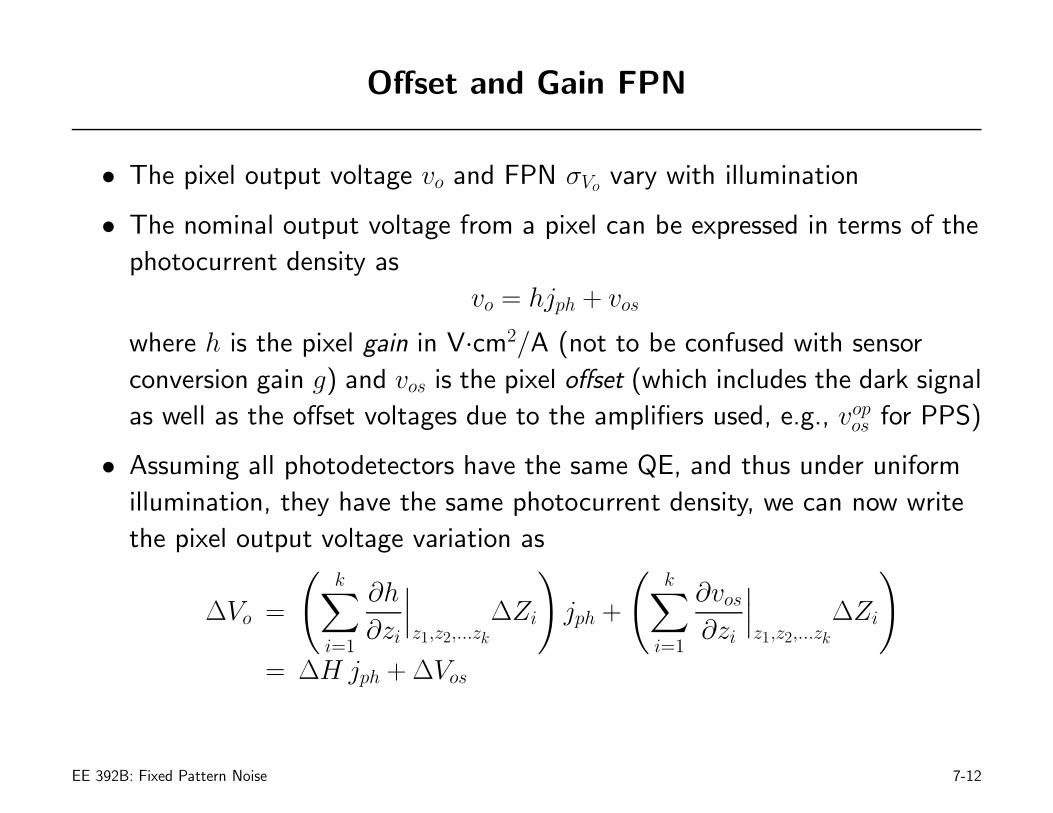
Offset and Gain FPN
• The pixel output voltage vo and FPN σVo vary with illumination
• The nominal output voltage from a pixel can be expressed in terms of thephotocurrent density as
vo = hjph + vos
where h is the pixel gain in V·cm2/A (not to be confused with sensorconversion gain g) and vos is the pixel offset (which includes the dark signalas well as the offset voltages due to the amplifiers used, e.g., vop
os for PPS)
• Assuming all photodetectors have the same QE, and thus under uniformillumination, they have the same photocurrent density, we can now writethe pixel output voltage variation as
∆Vo =
(k!
i=1
∂h
∂zi
"""z1,z2,...zk
∆Zi
)jph +
(k!
i=1
∂vos
∂zi
"""z1,z2,...zk
∆Zi
)
= ∆H jph + ∆Vos
EE 392B: Fixed Pattern Noise 7-12

• We quantify offset FPN by σVos and gain FPN by σH · jph
• Offest FPN is reported as % of well capacity
• Gain FPN is referred to as Pixel Response Nonuniformity (PRNU) and isreported as % of gain factor variation, i.e., 100σH/h
• Note that ∆H and ∆Vos are not necessarily uncorrelated, since somedevice parameters can affect both offset and gain
EE 392B: Fixed Pattern Noise 7-13

Analysis of FPN in PPS
• The figure shows the device parameters considered
idc
AD vT , Col
vo
vREF + vopos
Cf
AD is the photodiode area, idc is its dark current, vopos is the opamp offset
voltage, Col is the overlap capacitance, and vT is the threshold voltage
EE 392B: Fixed Pattern Noise 7-14

• The output voltage in steady state is given by
vo = (Q + ColvT ) · 1
Cf+ vREF + vop
os,
where ColvT is the “feedthrough” charge (when the reset transistor isturned off), and the charge Q accumulated on the photodiode capacitance
Q = (jphAD + idc)tint
• The following table lists the absolute values of the parameter senitivities∂vo∂zi
and effect on FPN
Parameter Sensitivity Effect on FPN
ADtintCf
· jph pixel/gain
idctintCf
pixel/offset
vopos 1 column/offset
Cfidctint+ColvT
C2f
column/offset
+ADtintC2
f· jph column/gain
vTColCf
column/offset
ColvTCf
column/offset
EE 392B: Fixed Pattern Noise 7-15

• Offset FPN
σVos =
#$$%&
tint
Cfσidc
'2
+ σ2vopos
+
((idctint + ColvT
C2f
)σCf
)2
+
&vT
CfσCol
'2
+
&Col
CfσvT
'2
• Gain FPN
σH · jph = jph
#$$%&
tint
CfσAD
'2
+
(ADtint
C2f
σCf
)2
• Pixel FPN
σX =
*&jphtint
CfσAD
'2
+
&tint
Cfσidc
'2
• Column FPN
σY =
#$$%σ2vopos
+
((idctint + ColvT + ADjphtint
C2f
)σCf
)2
+
&vT
CfσCol
'2
+
&Col
CfσvT
'2
• Note that the FPN variance σ2Vo
= σ2X + σ2
Y can be written as the sum ofthree terms, a term that is independent of the signal, a term thatincreases linearly with the signal, and a term that increases quadraticallywith the signal
EE 392B: Fixed Pattern Noise 7-16

Example
• Assume the following device parameter means, standard deviations, andthat tint = 30ms
Parameter Mean σ Sensitivity
AD 50µm2 0.4%AD 15 × 103jphV/µm2
idc 5fA 2%idc 1.5mV/fAvop
os 0V 2mV 1
Cf 20fF 0.2%Cf 11.6 × 10¹¹V/F37500jphV/fF
vTR 0.8V 0.2%vTR 0.02
Col 0.4fF 0.4%Col 0.04V/fF
EE 392B: Fixed Pattern Noise 7-17

• Offset FPN
Parameter Contribution to σVos
idc 0.15 mVvop
os 2 mVCf 0.0464 mVvTR 0.032 mVCol 0.064 mV
andσVos ≈ 2mV,
which is basically equal to the opamp offset σvopos
value
• Gain FPN at jph = 2.64 × 10⁻⁶A/cm2 (high illumination)
Parameter Contribution to σH · jph
AD 7.92 mVCf 3.96 mV
andσH · jph = 8.85mV
EE 392B: Fixed Pattern Noise 7-18

• The following figure plots total FPN σVo, pixel FPN σX, and column FPNσY , assuming monochromatic illumination F0 photons/cm2.s at quantumefficiency QE = 0.3
1012 1013 10140
1
2
3
4
5
6
7
8
9
10
illumination Fo (photon/cm2 s)
FPN
(mV)
Pixel FPNColumn FPNTotal FPN
EE 392B: Fixed Pattern Noise 7-19

Analysis of FPN in APS
idc
AD
vTR, ColR
vo
vTF , WF
LF
CD
ibias
vDDvDD
• In steady state and assuming soft reset, the output voltage is given by
vo = vDD − vTR − Q
CD−(
vTF +
+2LF
knWFibias
),
where the charge accumulted on the photodiode is given by
Q = (ADjph + idc)tint + ColRvDD
The ColRvDD term is the “feedthrough” charge (when the reset transistoris turned off)
EE 392B: Fixed Pattern Noise 7-20

Example
• Consider the following parameter means and standard deviations
parameter mean σ effect on FPN
idc 5fA 2%idc pixel/offsetAD 50µm2 0.4%AD pixel/gainCD 20fF 0.4%CD pixel/offset,gainvTR 1.1V 0.2%vTR pixel/offsetColR 0.4fF 0.4%ColR pixel/pffsetvTF 0.9V 0.2%vTF pixel/offsetWFLF
42 0.2%WF
LFpixel/offset
ibias 1.88µA 1%ibias column/offset
• You will compute the FPN component values in the homework
EE 392B: Fixed Pattern Noise 7-21

Image Sensor Total Noise Model
• Combining temporal noise and FPN, we can express the total inputreferred noise charge as
Qn = Qshot + Qreset + Qreadout + Qfpn,
where
◦ Qshot is the r.v. representing the noise charge due to photodetectorphoto and dark current shot noise and is Gaussian with zero meanand variance 1
q(iph + idc)tint electrons2
◦ Qreset is the r.v. representing the reset noise and is basicallyindependent of the signal
◦ Qreadout is the r.v. representing the readout circuit noise (possiblyincluding quantization) and is basically independent of the signal
EE 392B: Fixed Pattern Noise 7-22

◦ Qfpn is the r.v. representing FPN (in electrons), and can berepresented either as a sum of pixel and column components
Qfpn =1
g(X + Y )
where g is the sensor conversion gain in V/electron,or offset and gain components
Qfpn =1
g(∆Hjph + ∆Vos)
Thus it has one component that is independent of signal and onethat grows with the signal
◦ The noise components are assumed independent
• Thus the total average noise power is the sum of three components:
◦ One that does not depend on the signal (due to reset and readoutnoise and offset FPN)
◦ One that increases linearly with the signal (iph or jph) (due to shotnoise and gain FPN)
◦ One that increases quadratically with the signal (due to gain FPN)
EE 392B: Fixed Pattern Noise 7-23

Noise as Function of Photocurrent
10−16 10−15 10−14 10−13 10−12 10−1110−7
10−6
10−5
10−4
10−3
iph (A)
Ave
rage
Noise
pow
er(V
2 )
EE 392B: Fixed Pattern Noise 7-24

Correlated Double Sampling (CDS)
• CDS is a multiple sampling technique commonly used in image sensors toreduce FPN, and reset and 1/f noise
• You sample the output twice; once right after reset and a second timewith the signal present. The output signal is the difference between thetwo samples
◦ CDS only reduces offset FPN (does not reduce gain FPN)
◦ CDS does not cancel offset FPN due to dark current variation
◦ In CCDs, PPS, photogate and pinned diode APS, CDS cancels resetnoise. In photodiode APS it increases it
EE 392B: Fixed Pattern Noise 7-25

CDS in PPS
Word
Reset
Reset
SS
SR
SR
CoS
CoR
Word, SS
EE 392B: Fixed Pattern Noise 7-26

• Cancells
◦ FPN due to vopos, vT , and Col
◦ Temporal noise due to reset (terms V 2o2 and V 2
o3 in our analysis)
◦ Readout noise due to op-amp 1/f noise
• Does not cancel
◦ Offset FPN due to idc variation. This is called Dark SignalNon-uniformity (DSNU)
◦ Gain FPN (or PRNU)
◦ Other temporal noise components
• Adds
◦ Opamp noise due to reset read (V 2o4 term)
◦ KTC noise due to SS and SR transistors
EE 392B: Fixed Pattern Noise 7-27

• To summarize, the total noise charge for the two samples are given by:
Qn1 = Qreset + Qread1 + Qfpn1
Qn2 = Qshot + Qreset + Qreadout2 + Qfpn2
Note that Qfpn1 is simply an offset FPN whereas Qfpn2 is the sum of offsetand gain FPN (PRNU). However, Qfpn1 does not include the offset FPNdue to dark current variation (DSNU), whereas the offset part of Qfpn1
includes it
The difference between the two samples is thus:
Qn2 − Qn1 = Qshot + (Qreadout2 − Qreadout1) + Qprnu + Qdsnu
EE 392B: Fixed Pattern Noise 7-28

PPS FPN With and Without CDS
• The following figure plots PPS FPN with and without CDS (assumingthat vop
os, vT , and Col are eliminated)
1012 1013 10140
1
2
3
4
5
6
7
8
9
10
illumination Fo (photon/cm2 s)
FPN
(mV)
CDSw/o CDS
EE 392B: Fixed Pattern Noise 7-29

PPS Offset FPN With and Without CDS
10 20 30 40 50 60
10
20
30
40
50
60
10 20 30 40 50 60
10
20
30
40
50
60
without CDS with CDS
EE 392B: Fixed Pattern Noise 7-30

CDS in 3T APS
Word
Word
Reset
Reset
SS
SS
SR
SR
CoS
CoR
EE 392B: Fixed Pattern Noise 7-31

• Cancells
◦ All offset FPN terms involving vTR, vTF , ColR, WFLF
, and ibias
• Does not cancel
◦ DSNU
◦ Reset noise
◦ PRNU
◦ Readout noise
• Adds
◦ Reset noise kT2CD
(reset noise component during reset readoutindependent of that during signal readout)
◦ Readout noise during reset readout
◦ kTC due to SS and SR transistors
EE 392B: Fixed Pattern Noise 7-32

• To summarize, the total noise charge for the two samples are given by:
Qn1 = Qshot + Qreset1 + Qreadout1 + Qfpn1
Qn2 = Qreset2 + Qreadout2 + Qfpn2
The difference is:
Qn1 − Qn2 = Qshot + (Qreset1 − Qreset2) + (Qread1 − Qread2) + Qprnu + Qdsnu
• An important advantage of photogate and pinned diode APS is that resetnoise is eliminated using CDS instead of doubled
EE 392B: Fixed Pattern Noise 7-33