Embed Size (px)
Citation preview

USER’S MANUAL
AN1630Rev 1.00
May 17, 2011
ISL8016CIR1EVAL1Z6A Low Quiescent Current High Efficiency Synchronous Buck Regulator
DescriptionThe ISL8016CIR1EVAL1Z kit is intended for use by individuals with requirements for Point-of-Load applications sourcing from 2.7V to 5.8V. The ISL8016CIR1EVAL1Z simple smallest factor evaluation board is used for a quick and easy demonstration of the performance of the ISL8016 low quiescent high efficiency synchronous buck regulator.
The ISL8016 is offered in a 3mmx4mm 20 Ld QFN package with 1mm maximum height. The complete converter occupies can be as small as 0.15in2 area.
Key Features• High Efficiency Synchronous Buck Regulator with up to 97%
Efficiency
• 0.8% Reference Accuracy Over-Temperature/Load/Line
• Fixed Output Voltage Option
• ±10% Output Voltage Margining
• Adjustable Current Limit
• Current Sharing Capable
• Start-up with Pre-Biased Output
• Internal Soft-Start - 1ms or Adjustable
• Soft-Stop Output Discharge During Disabled
• Adjustable Frequency from 500kHz to 4MHz - Default at 1MHz
• External Synchronization up to 4MHz - Master to Slave Phase Shifting Capability
Recommended EquipmentThe following materials are recommended to perform testing:
• 0V to 10V Power Supply with at least 10A source current capability or 5V battery
• Electronic Loads capable of sinking current up to 7A
• Digital Multimeters (DMMs)
• 100MHz quad-trace oscilloscope
• Signal generator
Quick Setup Guide 1. Ensure that the circuit is correctly connected to the supply
and loads prior to applying any power.
2. Connect the bias supply to VIN, the plus terminal to VIN, J1, and the negative return to PGND, J2.
3. Connect the output load to VOUT, the plus terminal to VOUT1, J3 and the negative return to PGND, J4.
4. Verify that the position is PWM for S1.
5. Verify the position is OPEN for S2 and S3.
6. Verify that the position is ON for S4 and S5.
7. Turn on the power supply.
8. Verify the output voltage is 1.8V for VOUT1.
Evaluating the Other Output VoltageThe ISL8016CIR1EVAL1Z kit output is preset to 1.8V for VOUT1, however, output voltages can be adjusted from 0.6V to 5V. The output voltage programming resistor, R1, will depend on the desired output voltage of the regulator. The value for the feedback resistor is typically between 0 and 200k as shown in Equation 1.
If the output voltage desired is 0.6V, then R2 is left unpopulated and R1 is shorted. For faster response performance, add 10pF to 47pF in parallel to R1. Check bode plot to insure optimum performance.
Frequency ControlISL8016 has an FS pin that controls the frequency of operation. Programmable frequency allows for optimization between efficiency and external component size. Default switching frequency is 1MHz when FS is tied to VIN (R6 = 0 and R5 is open). By connecting R5 to GND, the switching frequency could be changed from 500kHz (R5 = 390k) to 4MHz (R5 = 40k) according to Equation 2:
When using R5 to adjust the operational frequency, this also sets external compensation mode. Please refer to the ISL8016 datasheet (FN7616) for more details.
R2 R1VFB
VO VFB–------------------------ = (EQ. 1)
RT k 200 103fOSC kHz ------------------------------ 10–= (EQ. 2)
AN1630 Rev 1.00 Page 1 of 12May 17, 2011

ISL8016CIR1EVAL1Z
Soft-Start ControlShort CSS1 to SGND for internal soft-start (approximately 1ms). Populate CSS1 to adjust the soft-start time. This capacitor, along with an internal 1.6mA current source, sets the soft-start interval of the converter, tSS.
CSS must be less than 33nF to insure proper soft-start reset after fault condition.
Synchronization ControlThe ISL8016 can be synchronized from 700kHz to 4MHz by an external signal applied to the SYNCIN pin. The rising edge on the SYNCIN triggers the rising edge of the PHASE pulse. Make sure that the minimum on-time of the PHASE node is greater than 140ns.
SYNCOUT is a 250µA current pulse signal output triggered by the rising edge of the clock or the SYNCIN signal (whichever is greater in frequency) to drive the other ISL8016 and avoid the system’s beat frequencies effects. To implement time shifting between the master circuit to the slave, it is recommended to add a capacitor, C13 as shown in the schematic. The time delay from SYNCOUT_Master to SYNCIN_Slave is calculated in pF using the following:
Where, t is the desired time shift between the master and theslave circuits in ns. Care must be taken to include PCB parasiticcapacitance of ~3pF to 10pF.
The maximum should be limited to 1/Fs-100ns to insure that SYNCOUT has enough time to discharge before the next cycle starts.
Swtiches ControlThe ISL8016 evaluation board contains S1 thru S5 for various controls of the ISL8016 circuitries. Table 1 details this function.
CSS1 F 3.33 tSS s = (EQ. 3)
C6 pF 0.357 t ns = (EQ. 4)
TABLE 1. SWITCH SETTINGS
S1 MODE FUNCTION
1 PWM Fixed PWM frequency at light load
3 PFM Force continuous mode
S2 ISET PROGRAM OUTUT CURRENT
1 LOW SET OUTPUT LOAD TO 2A.
- OPEN SET OUTPUT LOAD TO 6A.
3 HIGH SET OUTPUT LOAD TO 4A.
S3 VSET SET OUTPUT MARGIN
1 LOW SET OUTPUT VOLTAGE -10%.
- OPEN NO OUTPUT VOLTAGE MARGIN
3 HIGH SET OUTPUT VOLTAGE +10%.
S4 ENABLE FUNCTION
1 OFF DISABLE VOUT1
3 PFM ENABLE VOUT1
S5 ENABLE FUNCTION
1 OFF DISABLE VOUT2
3 PFM ENABLE VOUT2
AN1630 Rev 1.00 Page 2 of 12May 17, 2011

AN
16
30R
ev 1.0
0P
age 3 of 1
2M
ay 17, 20
11
ISL8
016
CIR
1EV
AL
1Z
GND
PGND
SE KEEP FB1, FB2 PINS TRACES SHORTSE KEEP COMP PIN TRACES SHORT
EVALUATION BOARD
ISL8016
VOUT1C9OPEN
JUN XIAO
ISL8016
SCHEMATIC
A
/09
VOUT2
J6
J5
4
3
C10
R15
J4
14
3
2
C4
C8
J3
OPEN22UF
OPEN
47PFJC111_07XX
JC111_07XX
VOUT1
VOUT2
HRDWR ID
R
MASK# REV.
DATE:ENGINEER:
TITLE:
A
A
A A
ISL8016CIR1EVAL1Z Schematic
PGND
ON/EXPFM
OFF
ON/EX
ON/EXOFF
OFF
P
PLEAPLEA
NOTE:
OFF
VIN
ON/EXPWMVIN
7
13VSET
FS1
DNP
13VS
ET
OPEN
R9
VSET
C27
R19
22UF
SYNCIN2
11 12
ISETEN2
FS2
C26
VIN
0.68UH
C21
22UF
3
2N7002
LX2 1
SYNCOUT1
JC111_07XX
22UF
C20
JC111_07XXJ1
S5
R11
2N7002
Q1PG2
220PFISET
C14
100K
330PF
ISL8016IRZ
C23
SYNCIN11.0UH
20R28
06/11JUN XIAO
C17
SYNCIN1
R5
21
9
8
7
6 5 4 3
20
2
19
18
17
161514131211
10
1
U3
21
9
8
7
6 5 4 3
20
2
19
18
17
161514
10
1
SLAVE
21
9
8
6 5 4 3 2
19
18
17
1615141211
10
1
MASTER
R26R16
21
L3
SYNCIN3
R7
R29
R25
C22 C24
C25
FB2
CSS2
C1R24
C11C12
R22
R21
C13
EN2
1
32
R23
R4
R13
R14
PG2
23
Q2
12
D2
R27
4
3
2
SYNCOUT2
R20
SS2
L2
C18 C19
12
R6
C2
C6
CSS1
EN1
R12
1
32 S4
12 S3
1
32 S2
C3
PG1
ISET
14
3
2 LX1
R8R10
1
32 S1
R17
R18
2
1
312
D1 C5
R2 R1
C7
L1
R3
J2
DNP
VIN
SYNCIN1
SS1
0
OPEN
ISL8016IRZ
VIN
100K
200K 47PF
22UF
0
100K
1.0UH
VIN
OPEN
SS2
SS247K
22UF
200K47PF
100K
0
FB2
VOUT2
OPEN OPEN
PG2
DNP
VIN
EN1
2K
FB1
COMP2
200K
COMP1
22UF20
22UF
PG1
VOUT2
22UF
100K
VIN
100K
22UF
VIN200K
2K
VIN
22UF
VINEN2
ISL8016IRZ
VSET
22UF
OPEN
ISET
100K
100K
PG1
100K100K
OPEN
0
0
100KFB2
VIN
VIN
OPEN
DNP
EN1EN2
COMP2COMP2
1
RELEASED BY:
DRAWN BY: DATE:
DATE:
DATE:
TESTE
UPDATED BY:E
P
PGND
VFB
VIN
VIN
PG
SYNCOUT
SYNCIN
PGND
SGND
ISE
TS
SC
OM
PFSV
SE
T
EN
LX PG
ND
LXLXVIN
EP
PGND
VFB
VIN
VIN
PG
SYNCOUT
SYNCIN
PGND
SGND
ISE
TS
SC
OM
PFSV
SE
T
EN
LX PG
ND
LXLXVIN
A
EP
PGND
VFB
VIN
VIN
PG
SYNCOUT
SYNCIN
PGND
SGND
ISE
TS
SC
OM
PFSV
SE
T
EN
LX PG
ND
LXLXVIN
A A
A
A
A
A
A
A
A
A
A
A
A
A
A
A
A
A
A
A
A
A
A
A

ISL8016CIR1EVAL1Z
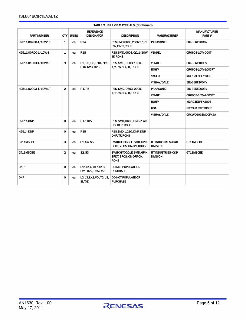
TABLE 2. BILL OF MATERIALS
PART NUMBER QTY UNITSREFERENCE DESIGNATOR DESCRIPTION MANUFACTURER
MANUFACTURER PART #
ISL8016CIR1EVAL1ZREVAPCB 1 ea SEE LABEL-RENAME BOARD
PWB-PCB, ISL8016CIR1EVAL1Z, REVA, ROHS
TBD ISL8016CIR1EVAL1ZREVAPCB
H1045-00150-50V5-T 1 ea C4 CAP, SMD, 0603, 15pF, 50V, 5%, NPO, ROHS
MURATA GRM39COG150J050AD
H1045-00221-50V5-T 1 ea C5 CAP, SMD, 0603, 220pF, 50V, 5%, C0G, ROHS
VENKEL C0603COG500-221JNE
H1045-00333-50V5-T 1 ea CSS1 CAP, SMD, 0603, 33000pF, 25V, 5%, X7R, ROHS
AVX 06035C333JAT2A
H1045-DNP 0 ea C3, C6, CSS2 CAP, SMD, 0603, DNP-PLACE HOLDER, ROHS
MURATA GRM36COG680J050AQ
H1065-00226-6R3V20-T 5 ea C1, C2, C7,C8, C10
CAP, SMD, 1206, 22µF, 6.3V, 20%, X5R, ROHS
H1065-00476-6R3V20-T 1 ea C9 CAP, SMD, 1206, 47µF, 6.3V, 20%, X5R, ROHS
MURATA GRM31CR60J476ME19L
H1065-DNP 0 ea C19, C20, C23, C24
CAP, SMD, 1206, DNP-PLACE HOLDER, ROHS
IHLP-5050CE-01-1R0M 1 ea L1 COIL-PWR INDUCTOR, SMD, 13mm, 1.0µH, 20%, 24A, ROHS
VISHAY IHLP-5050CE-01-1R0M
111-0702-001 2 ea J1, J3 CONN-GEN, BIND.POST, INSUL-RED, THMBNUT-GND
JOHNSON COMPONENTS 111-0702-001
111-0703-001 2 ea J2, J4 CONN-GEN, BIND.POST, INSUL-BLK, THMBNUT-GND
JOHNSON COMPONENTS 111-0703-001
131-4353-00 2 ea LX1, VOUT1 CONN-SCOPE PROBE TEST PT, COMPACT, PCB MNT, ROHS
TEKTRONIX 131-4353-00
1514-2 2 ea J5, J6 CONN-TURRET, TERMINAL POST, TH, ROHS
KEYSTONE 1514-2
5000 14 ea EN1, EN2, FB2, PG1, PG2, SS2, ISET, VSET, COMP2, SYNCIN1-SYNCIN3, SYNCOUT1, SYNCOUT2
CONN-MINI TEST PT, VERTICAL, RED, ROHS
KEYSTONE 5000
LTST-C170CKT 2 ea D1, D2 LED-GaAs RED, SMD, 2X1.25mm, 100mW, 40mA, 10mcd, ROHS
LITEON/VISHAY LTST-C170CKT
B340B-13-F-T 2 ea D1, D2 DIODE-SCHOTTKY, SMD, SMB, 2P, 40V, 3A, ROHS
DIODES INC. B340B-13-F
ISL8016IRZ 1 ea MASTER IC-ADJ. 6A BUCK REGULATOR, 20P, QFN, 3X4, ROHS
INTERSIL ISL8016IRZ
2N7002-7-F-T 2 ea Q1, Q2 TRANSISTOR, N-CHANNEL, 3 LD, SOT23, 60V, 115mA, ROHS
DIODES, INC. 2N7002-7-F
H2505-DNP 0 ea R6, R9 ,R20, R28 RESISTOR,SMD,0603,0.1%,MF,DNP-PLACE HOLDER
H2510-DNP 0 ea R4, R7, R13, R14, R19, R21, R22, R25, R29
RES,SMD,0402, DNP, DNP, DNP,TF,ROHS
AN1630 Rev 1.00 Page 4 of 12May 17, 2011
ISL8016CIR1EVAL1Z
H2511-00200-1/10W1-T 1 ea R24 RES,SMD,0603,20ohm,1/10W,1%,TF,ROHS
PANASONIC ERJ-3EKF20R0V
H2511-00R00-1/10W-T 1 ea R18 RES, SMD, 0603, 0Ω, 1/10W, TF, ROHS
VENKEL CR0603-10W-000T
H2511-01003-1/10W1-T 9 ea R2, R3, R8, R10-R12, R16, R23, R26
RES, SMD, 0603, 100k, 1/10W, 1%, TF, ROHS
VENKEL ERJ-3EKF1003V
ROHM CR0603-10W-1003FT
YAGEO MCR03EZPFX1003
VISHAY/DALE ERJ-3EKF1004V
H2511-02003-1/10W1-T 2 ea R1, R5 RES, SMD, 0603, 200k, 1/10W, 1%, TF, ROHS
PANASONIC ERJ-3EKF2003V
VENKEL CR0603-10W-2003FT
ROHM MCR03EZPFX2003
KOA RK73H1JTTD2003F
VISHAY/DALE CRCW06031M00FKEA
H2511-DNP 0 ea R17, R27 RES, SMD, 0603, DNP-PLACE HOLDER, ROHS
H2514-DNP 0 ea R15 RES,SMD, 1210, DNP, DNP, DNP, TF, ROHS
GT11MSCBE-T 3 ea S1, S4, S5 SWITCH-TOGGLE, SMD, 6PIN, SPDT, 2POS, ON-ON, ROHS
ITT INDUSTRIES/C&K DIVISION
GT11MSCBE
GT13MSCBE 2 ea S2, S3 SWITCH-TOGGLE, SMD, 6PIN, SPDT, 3POS, ON-OFF-ON, ROHS
ITT INDUSTRIES/C&K DIVISION
GT13MSCBE
DNP 0 ea C11-C14, C17, C18, C21, C22, C25-C27
DO NOT POPULATE OR PURCHASE
DNP 0 ea L2, L3, LX2, VOUT2, U3, SLAVE
DO NOT POPULATE OR PURCHASE
TABLE 2. BILL OF MATERIALS (Continued)
PART NUMBER QTY UNITSREFERENCE DESIGNATOR DESCRIPTION MANUFACTURER
MANUFACTURER PART #
AN1630 Rev 1.00 Page 5 of 12May 17, 2011

ISL8016CIR1EVAL1Z
ISL8016CIR1EVAL1Z Board Layout
FIGURE 1. TOP LAYER COMPONENTS
ISL8016CIR1EVAL1Z
AN1630 Rev 1.00 Page 6 of 12May 17, 2011

ISL8016CIR1EVAL1Z
FIGURE 2. TOP LAYER ETCH
ISL8016CIR1EVAL1Z Board Layout (Continued)
AN1630 Rev 1.00 Page 7 of 12May 17, 2011

ISL8016CIR1EVAL1Z
FIGURE 3. SECOND LAYER ETCH
ISL8016CIR1EVAL1Z Board Layout (Continued)
AN1630 Rev 1.00 Page 8 of 12May 17, 2011

ISL8016CIR1EVAL1Z
FIGURE 4. THIRD LAYER ETCH
ISL8016CIR1EVAL1Z Board Layout (Continued)
AN1630 Rev 1.00 Page 9 of 12May 17, 2011

ISL8016CIR1EVAL1Z
FIGURE 5. BOTTOM LAYER ETCH
ISL8016CIR1EVAL1Z Board Layout (Continued)
AN1630 Rev 1.00 Page 10 of 12May 17, 2011

ISL8016CIR1EVAL1Z
FIGURE 6. BOTTOM LAYER COMPONENTS
ISL8016CIR1EVAL1Z Board Layout (Continued)
AN1630 Rev 1.00 Page 11 of 12May 17, 2011

http://www.renesas.comRefer to "http://www.renesas.com/" for the latest and detailed information.
Renesas Electronics America Inc.1001 Murphy Ranch Road, Milpitas, CA 95035, U.S.A.Tel: +1-408-432-8888, Fax: +1-408-434-5351Renesas Electronics Canada Limited9251 Yonge Street, Suite 8309 Richmond Hill, Ontario Canada L4C 9T3Tel: +1-905-237-2004Renesas Electronics Europe LimitedDukes Meadow, Millboard Road, Bourne End, Buckinghamshire, SL8 5FH, U.KTel: +44-1628-651-700, Fax: +44-1628-651-804Renesas Electronics Europe GmbHArcadiastrasse 10, 40472 Düsseldorf, Germany Tel: +49-211-6503-0, Fax: +49-211-6503-1327Renesas Electronics (China) Co., Ltd.Room 1709 Quantum Plaza, No.27 ZhichunLu, Haidian District, Beijing, 100191 P. R. ChinaTel: +86-10-8235-1155, Fax: +86-10-8235-7679Renesas Electronics (Shanghai) Co., Ltd.Unit 301, Tower A, Central Towers, 555 Langao Road, Putuo District, Shanghai, 200333 P. R. China Tel: +86-21-2226-0888, Fax: +86-21-2226-0999Renesas Electronics Hong Kong LimitedUnit 1601-1611, 16/F., Tower 2, Grand Century Place, 193 Prince Edward Road West, Mongkok, Kowloon, Hong KongTel: +852-2265-6688, Fax: +852 2886-9022Renesas Electronics Taiwan Co., Ltd.13F, No. 363, Fu Shing North Road, Taipei 10543, TaiwanTel: +886-2-8175-9600, Fax: +886 2-8175-9670Renesas Electronics Singapore Pte. Ltd.80 Bendemeer Road, Unit #06-02 Hyflux Innovation Centre, Singapore 339949Tel: +65-6213-0200, Fax: +65-6213-0300Renesas Electronics Malaysia Sdn.Bhd.Unit 1207, Block B, Menara Amcorp, Amcorp Trade Centre, No. 18, Jln Persiaran Barat, 46050 Petaling Jaya, Selangor Darul Ehsan, MalaysiaTel: +60-3-7955-9390, Fax: +60-3-7955-9510Renesas Electronics India Pvt. Ltd.No.777C, 100 Feet Road, HAL 2nd Stage, Indiranagar, Bangalore 560 038, IndiaTel: +91-80-67208700, Fax: +91-80-67208777Renesas Electronics Korea Co., Ltd.17F, KAMCO Yangjae Tower, 262, Gangnam-daero, Gangnam-gu, Seoul, 06265 KoreaTel: +82-2-558-3737, Fax: +82-2-558-5338
SALES OFFICES
© 2018 Renesas Electronics Corporation. All rights reserved.Colophon 7.0
(Rev.4.0-1 November 2017)
Notice
1. Descriptions of circuits, software and other related information in this document are provided only to illustrate the operation of semiconductor products and application examples. You are fully responsible for
the incorporation or any other use of the circuits, software, and information in the design of your product or system. Renesas Electronics disclaims any and all liability for any losses and damages incurred by
you or third parties arising from the use of these circuits, software, or information.
2. Renesas Electronics hereby expressly disclaims any warranties against and liability for infringement or any other claims involving patents, copyrights, or other intellectual property rights of third parties, by or
arising from the use of Renesas Electronics products or technical information described in this document, including but not limited to, the product data, drawings, charts, programs, algorithms, and application
examples.
3. No license, express, implied or otherwise, is granted hereby under any patents, copyrights or other intellectual property rights of Renesas Electronics or others.
4. You shall not alter, modify, copy, or reverse engineer any Renesas Electronics product, whether in whole or in part. Renesas Electronics disclaims any and all liability for any losses or damages incurred by
you or third parties arising from such alteration, modification, copying or reverse engineering.
5. Renesas Electronics products are classified according to the following two quality grades: “Standard” and “High Quality”. The intended applications for each Renesas Electronics product depends on the
product’s quality grade, as indicated below.
"Standard": Computers; office equipment; communications equipment; test and measurement equipment; audio and visual equipment; home electronic appliances; machine tools; personal electronic
equipment; industrial robots; etc.
"High Quality": Transportation equipment (automobiles, trains, ships, etc.); traffic control (traffic lights); large-scale communication equipment; key financial terminal systems; safety control equipment; etc.
Unless expressly designated as a high reliability product or a product for harsh environments in a Renesas Electronics data sheet or other Renesas Electronics document, Renesas Electronics products are
not intended or authorized for use in products or systems that may pose a direct threat to human life or bodily injury (artificial life support devices or systems; surgical implantations; etc.), or may cause
serious property damage (space system; undersea repeaters; nuclear power control systems; aircraft control systems; key plant systems; military equipment; etc.). Renesas Electronics disclaims any and all
liability for any damages or losses incurred by you or any third parties arising from the use of any Renesas Electronics product that is inconsistent with any Renesas Electronics data sheet, user’s manual or
other Renesas Electronics document.
6. When using Renesas Electronics products, refer to the latest product information (data sheets, user’s manuals, application notes, “General Notes for Handling and Using Semiconductor Devices” in the
reliability handbook, etc.), and ensure that usage conditions are within the ranges specified by Renesas Electronics with respect to maximum ratings, operating power supply voltage range, heat dissipation
characteristics, installation, etc. Renesas Electronics disclaims any and all liability for any malfunctions, failure or accident arising out of the use of Renesas Electronics products outside of such specified
ranges.
7. Although Renesas Electronics endeavors to improve the quality and reliability of Renesas Electronics products, semiconductor products have specific characteristics, such as the occurrence of failure at a
certain rate and malfunctions under certain use conditions. Unless designated as a high reliability product or a product for harsh environments in a Renesas Electronics data sheet or other Renesas
Electronics document, Renesas Electronics products are not subject to radiation resistance design. You are responsible for implementing safety measures to guard against the possibility of bodily injury, injury
or damage caused by fire, and/or danger to the public in the event of a failure or malfunction of Renesas Electronics products, such as safety design for hardware and software, including but not limited to
redundancy, fire control and malfunction prevention, appropriate treatment for aging degradation or any other appropriate measures. Because the evaluation of microcomputer software alone is very difficult
and impractical, you are responsible for evaluating the safety of the final products or systems manufactured by you.
8. Please contact a Renesas Electronics sales office for details as to environmental matters such as the environmental compatibility of each Renesas Electronics product. You are responsible for carefully and
sufficiently investigating applicable laws and regulations that regulate the inclusion or use of controlled substances, including without limitation, the EU RoHS Directive, and using Renesas Electronics
products in compliance with all these applicable laws and regulations. Renesas Electronics disclaims any and all liability for damages or losses occurring as a result of your noncompliance with applicable
laws and regulations.
9. Renesas Electronics products and technologies shall not be used for or incorporated into any products or systems whose manufacture, use, or sale is prohibited under any applicable domestic or foreign laws
or regulations. You shall comply with any applicable export control laws and regulations promulgated and administered by the governments of any countries asserting jurisdiction over the parties or
transactions.
10. It is the responsibility of the buyer or distributor of Renesas Electronics products, or any other party who distributes, disposes of, or otherwise sells or transfers the product to a third party, to notify such third
party in advance of the contents and conditions set forth in this document.
11. This document shall not be reprinted, reproduced or duplicated in any form, in whole or in part, without prior written consent of Renesas Electronics.
12. Please contact a Renesas Electronics sales office if you have any questions regarding the information contained in this document or Renesas Electronics products.
(Note 1) “Renesas Electronics” as used in this document means Renesas Electronics Corporation and also includes its directly or indirectly controlled subsidiaries.
(Note 2) “Renesas Electronics product(s)” means any product developed or manufactured by or for Renesas Electronics.