Embed Size (px)
Citation preview
Design and assembly of fast and lightweight barrel and forwardtracking prototype systems for an EIC
S. Aune, E. Delagnes , M. Garcon, I. Mandjavidze, S. Procureur, F. Sabatie1
CEA Saclay - Irfu
B. Surrow2
MIT / Temple University
D. Hasell, R. Milner, B. Redwine, G. van NieuwenhuizenMIT, Laboratory for Nuclear Science
B. Buck, J. BessuilleMIT, Bates Laboratory
1 Tracking detectors for an EIC
The necessary kinematical coverage for the EIC science case has been extensively reviewed in theINT report or the previous detector LOI earlier this year. The BNL and Jefferson Lab teams havecome up with a preliminary detector design, including details on several tracking systems neededto achieve the proposed physics case :
• Large radii tracking systems mostly located in the barrel region. This is not the purposeof this proposal since it involves R&D on very large detectors, the issue being mostly theirsize.
• Intermediate radii vertex tracking systems located both near the interaction point but alsoin the forward and backward regions. They are relatively large detectors (up to 0.5 m inradius), either planar or possibly cylindrical depending on the chosen technology. Thisintermediate area is the focus of this proposal.
• Small radii vertex tracking systems located as close to the interaction point as possible. Thetechnology of choice is thin Silicon pixels with integrated signal processing.
• Roman Pots may be needed at high values of proton energies: they are very small angletracking detectors designed to detect the recoil baryon close to the ion beam.
The intermediate radii vertex tracking system itself consists in two distinct areas :
• The barrel region, which would benefit from a cylindrical detector surrounding the interac-tion point and its µ-vertex detector and would go up to 0.5 m in radius from the IP.
• The forward and backward region which could be several stacks of planar detectors, circularin shape, with a hole in the middle to let the beams through.
These tracking regions of interest to us are slightly different in the case of eRHIC and MEIC/ELICand shown in yellow in Figures 1 and 2.
1Saclay proposal contact person, [email protected]/Temple University proposal contact person, [email protected]
1

Figure 1: Central detector layout of eRHIC.
Figure 2: Central detector layout of MEIC (Jefferson Lab).
2

This proposal describes the R&D needed both in the barrel and forward/backward regionfor the intermediate tracker. Firstly, a Micromegas-based cylindrical tracker, largely inspiredfrom the future CLAS12 Micromegas Vertex Tracker but larger in dimensions, would equip thebarrel region. The forward and backward regions would utilize large GEM chambers for thispurpose, similar to the forward GEM tracker. A zoom on the area concerned by this proposal isshown on Figure 3. Both types of detectors have common R&D in terms of electronics readoutand integration, which will be significant challenges for such detectors encapsulated inside the EICdetector. This is especially crucial for the barrel detectors, which cannot afford to have electronicschips imbedded into the detectors, since they need to be kept lightweight.
Figure 3: Intermediate vertex tracking area of EIC with forward region. The cylindrical detec-tors would include a µ-vertex tracker (not shown) and several layers of cylindrical Micromegaschambers. For the forward area, flat and relatively large GEM detectors will be studied within thisR&D proposal. On this schematic, the length of the cylindrical tracker would be about 1 m and itsradius 40 cm at the largest. The GEM counters have similar radius with a hole in the middle.
3

2 Micromegas mid-rapidity vertex tracker
2.1 From CLAS12 to EIC
A Micromegas (MICROMEsh GAseous Structure) is a gaseous detector based on a parallel plateelectrode structure and a set of microstrips or micropixels for readout. The presence of a mi-cromesh between the strips and the drift electrode allows for separating the conversion gap, whereparticles create primary electrons by interacting with the gas, from the amplification gap, wherethe primary electrons will create an avalanche in the presence of a high electric field. A schematicof a Micromegas detector is shown on Figure 4. If this field is high enough compared to the fieldin the conversion gap, the micromesh is transparent for the electrons, but not for the ions comingfrom the avalanche. This special feature allows a very fast collection of the ions created in theamplification gap (around 100 ns, compared to several microseconds for a drift chamber). For thisreason, Micromegas detectors have a very high-rate capability.
Figure 4: Schematic of a Micromegas detector.
The newly invented bulk technology for the Micromegas production adds to the advantagesof such detectors : they are obtained by the lamination of a Printed Circuit Board (PCB) withphoto-resist films. After a suitable insulation and chemical treatments, one obtains an array ofspacers (pillars) that hold the mesh permanently, and ensure a constant distance with the PCB(i.e., with the strips or pixels) over the whole sensitive area of the detector. Using this procedure,robust and large detectors can be easily built.
The end result is a lightweight detector, about 0.16% radiation length per layer, which hasa very low cost, especially compared to Silicon alternatives. It can be made in large sizes, anddue to the fact that the PCB may be relatively thin, can be curved in order to create cylindricaldetectors. Such a detector is currently under production for the CLAS12 central detector atJefferson Lab by the Saclay group (see Figure 5 + ref), and it is therefore natural to expend this
4

R&D in order to study the case of an intermediate vertex tracker for the EIC.
Figure 5: Cylindrical Micromegas (without drift electrode) used as a prototype for CLAS12.
The CLAS12 Micromegas Vertex Tracker is about 0.4 m long and 0.5 m at maximum radius.The EIC intermediate barrel tracker would probably be about twice as long at least and slightlylarger in radius. This significant increase in size requires additional R&D, both in the productionprocess but also in the readout electronics. The solution used in CLAS12 so far consists in 1 m-long flex and lightweight cables between the detectors and the front end electronics (analog +digital). It is unlikely that for an EIC, it will be possible to use such short cables and othersolutions will need to be examined. This R&D will be common with the forward and backwardGEM detectors in this proposal, which will also need to be relatively lightweight and still havetheir electronics readout close enough to the detector.
2.2 Electronics for a Micromegas vertex tracker
The Micromegas detectors used for particle tracking can only be operated at low gain to limitthe spark rates. This kind of technology permits the manufacturing of low-cost very large sizedetectors covering area up to 0.5 m2. The anodes of these large detectors are usually segmented inlong strips with capacitance of typically 100 pF, nearly one order magnitude larger than for silicondetectors. Moreover, this capacitance is increased by the interconnection ones, when for spaceconstraints the front end electronics is moved away from the detector. In these conditions, theexisting tracker Si readout chips, designed for less than 20pF detector capacitance, have reducedcharge collection efficiency and high noise leading to a poor signal/noise ratio leading to poordetection efficiency when connected to a detector operating at low gain.
The 64-channel DREAM ASIC (Figures 7 and Fig 8), developed by CEA-Saclay/Irfu for theMicromegas tracker of the CLAS12 experiment, has been designed to fulfill the specific require-ments of tracking using micro-pattern gaseous detectors with capacitance per channel in the rangeof 50-200 pF. Its specified noise is smaller than 1500 e− for 100 pF detector capacitance (2500 e−
for 200 pF) for a 100 ns shaping time. Its very front-end part consists of a charge preamplifier able
5
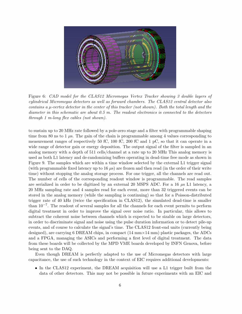
Figure 6: CAD model for the CLAS12 Micromegas Vertex Tracker showing 3 double layers ofcylindrical Micromegas detectors as well as forward chambers. The CLAS12 central detector alsocontains a µ-vertex detector in the center of this tracker (not shown). Both the total length and thediameter in this schematic are about 0.5 m. The readout electronics is connected to the detectorsthrough 1 m-long flex cables (not shown).
to sustain up to 20 MHz rate followed by a pole-zero stage and a filter with programmable shapingtime from 80 ns to 1 µs. The gain of the chain is programmable among 4 values corresponding tomeasurement ranges of respectively 50 fC, 100 fC, 200 fC and 1 pC, so that it can operate in awide range of detector gain or energy deposition. The output signal of the filter is sampled in ananalog memory with a depth of 511 cells/channel at a rate up to 20 MHz This analog memory isused as both L1 latency and de-randomizing buffers operating in dead-time free mode as shown inFigure 9. The samples which are within a time window selected by the external L1 trigger signal(with programmable fixed latency up to 16 µs) are frozen and then read (in the order of their writetime) without stopping the analog storage process. For one trigger, all the channels are read out.The number of cells of the corresponding readout window is programmable. The read samplesare serialized in order to be digitized by an external 20 MSPS ADC. For a 16 µs L1 latency, a20 MHz sampling rate and 4 samples read for each event, more than 32 triggered events can bestored in the analog memory (while the sampling is continuing) so that for a Poisson-distributedtrigger rate of 40 kHz (twice the specification in CLAS12), the simulated dead-time is smallerthan 10−7. The readout of several samples for all the channels for each event permits to performdigital treatment in order to improve the signal over noise ratio. In particular, this allows tosubtract the coherent noise between channels which is expected to be sizable on large detectors,in order to discriminate signal and noise using the pulse duration information or to detect pile-upevents, and of course to calculate the signal’s time. The CLAS12 front-end units (currently beingdesigned), are carrying 6 DREAM chips, in compact (14 mm×14 mm) plastic packages, the ADCsand a FPGA, managing the ASICs and performing a first level of digital treatment. The datafrom these boards will be collected by the MPD VME boards developed by INFN Genova, beforebeing sent to the DAQ.
Even though DREAM is perfectly adapted to the use of Micromegas detectors with largecapacitance, the use of such technology in the context of EIC requires additional developments:
• In the CLAS12 experiment, the DREAM acquisition will use a L1 trigger built from thedata of other detectors. This may not be possible in future experiments with an EIC and
6
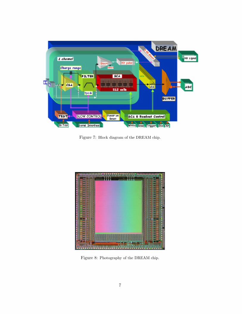
Figure 7: Block diagram of the DREAM chip.
Figure 8: Photography of the DREAM chip.
7

Figure 9: SCA used as a L1 circular buffer with frozen cells.
the tracker chips will need auto-triggering capabilities and the ability to provide fast signalsusable to build triggers. This feature is already available in the DREAM chip, as eachchannel includes a discriminator. The discriminator outputs are ORed to form a HIT chipoutput. This functionality, legacy from the former AGET chip, is not used on the front-endunits of CLAS12 and requires a special front-end board development. This study must bedone using a real size detector with a special focus on the minimum achievable thresholdand of this type of readout on the noise performances.
• In CLAS12, considering the very tight schedule and to minimize the risks, we have chosento move the front-end electronics away from the detector with the penalty of the extra costand noise due to long cables of the order 1 m. When using such detectors within the EICdetector, the space constraints will be higher and the electronics will be most likely be onthe detector PCB itself. To minimize multiple scatterings, it will be necessary to reduce thematerial in the detector including electronics. For this purpose, we also propose to study adetector prototype read by bare DREAM chips directly bonded on PCB (standard bondingor stub bonding).
2.3 Proposal for R&D studies
We propose to study and build a full scale 60◦ section prototype (50 cm radius) and therefore doR&D on the following aspects:
• Studies of auto-triggering capabilities of the DREAM ASIC
• Studies of on-detector chip solution for the DREAM ASIC
• Studies of large-size cables for readout
• Design of mechanical structure similar to the CLAS12 barrel tracker
• Design, production and test of large bulk and resistive Micromegas detectors at the Saclayworkshop
8

e± APV
mod
ule
Quarter section
Packaged APV chip
STAR Detector
TPC
BEMC
EEMC
FGT
FGT GEM foil
Figure 10: Layout of the STAR Forward GEM Tracker (FGT) together with photographs from leftto right showing a quarter section, an assembled disk based on four quarter sections, the actualarrangement of six disks and the overall carbon-fibre support structure.
It should be stressed that this prototyping efforts largely profits from the previous R&D madefor the CLAS12 Micromegas Tracker project. However, the challenges of both the extension insize and of the readout electronics are critical to applying this technology a future EIC.
3 GEM forward rapidity trackers
Forward tracking capabilities are an integral part of detector uprgrades and/or new detectorsystems for the future RHIC program and 12GeV program at JLab and in particular a future EICprogram. The usage of triple-GEM technology provides a cost-effective tracking solution featuringlow dead material and fast readout capabilities. GEM technology is widely employed by currentand future experiments in nuclear and particle physics. A SBIR3 proposal has been approved andis the basis for the development of the industrial production of GEM foils.
Figure 10 shows a side view of the STAR experiment with the location of six triple-GEMdetectors referring to the Forward GEM Tracker (FGT). The FGT covers the pseudo-rapidityrange of the STAR Endcap Electromagnetic Calorimeter (EEMC) of 1.09 < η < 2.
A photograph of a single FGT disk providing support for four independent triple-GEM detec-tors referred to as quarter sections is also shown in Figure 10. The inner radius of each quartersection is approximately 10.5 cm whereas the maximum outer radius is approximately 39 cm.
The quarter section layout takes into account the current size limitations of GEM foils by theTech-Etch Inc. production facility of approximately 50 × 50 cm2. A GEM foil is subdivided into
3SBIR (Small Business Innovation Research) is a highly competitive program within the Department of Energythat encourages small business to explore their technological potential and provides the incentive to profit from itscommercialization.
9
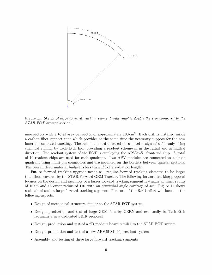
Figure 11: Sketch of large forward tracking segment with roughly double the size compared to theSTAR FGT quarter section.
nine sectors with a total area per sector of approximately 100 cm2. Each disk is installed insidea carbon fiber support cone which provides at the same time the necessary support for the newinner silicon-based tracking. The readout board is based on a novel design of a foil only usingchemical etching by Tech-Etch Inc. providing a readout scheme in in the radial and azimuthaldirection. The readout system of the FGT is employing the APV25-S1 front-end chip. A totalof 10 readout chips are used for each quadrant. Two APV modules are connected to a singlequadrant using multi-pin connectors and are mounted on the borders between quarter sections.The overall dead material budget is less than 1% of a radiation length.
Future forward tracking upgrade needs will require forward tracking elements to be largerthan those covered by the STAR Forward GEM Tracker. The following forward tracking proposalfocuses on the design and assembly of a larger forward tracking segment featuring an inner radiusof 10 cm and an outer radius of 110 with an azimuthal angle coverage of 45◦. Figure 11 showsa sketch of such a large forward tracking segment. The core of the R&D effort will focus on thefollowing aspects:
• Design of mechanical structure similar to the STAR FGT system
• Design, production and test of large GEM foils by CERN and eventually by Tech-Etchrequiring a new dedicated SBIR proposal
• Design, production and test of a 2D readout board similar to the STAR FGT system
• Design, production and test of a new APV25-S1 chip readout system
• Assembly and testing of three large forward tracking segments
10

It should be stressed that this prototyping efforts profits enormously from the lessons learnedby the STAR Forward GEM Tracker project. However, the extensions in size is a critical stepwhich requires care in the production and testing of GEM foils, the stretching of foils in generaland in particular the assembly of such a large structure.
4 Budget request
The total budget request for FY12/FY13 is $150k. Note that we plan to share a postdoctoralfellow during 2 years in order to help with studies and prototyping for both the barrel and forwardstudies. The budget break-down is as follows:
Barrel tracking budget request:
• Labor: $50k
• Material: $25k
The main focus of the following request is the production and testing of large curved Mi-cromegas detectors read-out with bare DREAM ASIC.
Forward tracking budget request:
• Labor: $50k
• Material: $25k
The main focus of the following request is the mechanical design and the production andtesting of large GEM foils.
11