Embed Size (px)
DESCRIPTION
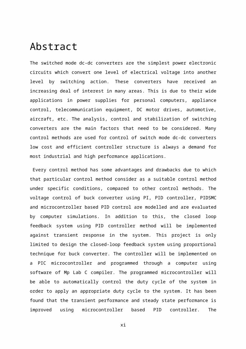
The switched mode dc-dc converters are the simplest power electronic circuits which convert one level of electrical voltage into another level by switching action. These converters have received an increasing deal of interest in many areas. This is due to their wide applications in power supplies for personal computers, appliance control, telecommunication equipment, DC motor drives, automotive, aircraft, etc. The analysis, control and stabilization of switching converters are the main factors that need to be considered. Many control methods are used for control of switch mode dc-dc converters low cost and efficient controller structure is always a demand for most industrial and high performance applications. Every control method has some advantages and drawbacks due to which that particular control method consider as a suitable control method under specific conditions, compared to other control methods. The voltage control of buck converter using PI, PID controller, PIDSMC and microcontroller based PID control are modelled and are evaluated by computer simulations. In addition to this, the closed loop feedback system using PID controller method will be implemented against transient response in the system. This project is only limited to design the closed-loop feedback system using proportional technique for buck converter. The controller will be implemented on a PIC microcontroller and programmed through a computer using software of Mp Lab C compiler. The programmed microcontroller will be able to automatically control the duty cycle of the system in order to apply an appropriate duty cycle to the system. It has been found that the transient performance and steady state performance is improved using microcontroller based PID controller. The experimental system is found to be more advantageous and cost effective with microcontroller.
Citation preview

Design and Implementation of Controller for Buck Converter
SESSION 2010
SUBMITTED BY:
Makhdoom Nawaz
(2010-EE-524)
Muhammad Waqas
(2010-EE-558)
SUPERVISED BY:
Engr. Moazzam Shehzad
Department of Electrical Engineering
Rachna College of Engineering and Technology, Gujranwala.
(A constituent college of University of Engineering and Technology, Lahore)

Design and Implementation of Controller for Buck Converter
Submitted to the faculty of the Electrical Engineering Department of the Rachna College of Engineering and Technology Gujranwala
in partial fulfillment of the requirements for the Degree of
Bachelor of Sciences
In
Electrical Engineering
_________________________ _________________________
Internal Examiner External Examiner
Department of Electrical Engineering
Rachna College of Engineering and Technology, Gujranwala.
(A constituent college of University of Engineering and Technology, Lahore)
Declaration
We, Makhdoom Nawaz and Muhammad Waqas, declare that the work presented in this thesis is our own, except where explicitly stated otherwise. In addition this work has not been submitted to obtain another degree or professional qualification.
Makhdoom Nawaz ______________________
Muhammad Waqas ______________________
Date: __________________
i

AcknowledgmentsCountless thanks to the Lord of the lords THE ALLAH ALMIGHTY, Creator of all of us, worthy of praises, Who blessed us with courage and power to complete our project and project report. And after Almighty ALLAH to His Prophet, Muhammad (S.A.W.W), the most perfect, Who is forever a source of guidance and knowledge for humanity as a whole.
We would like to thank our parents and all family members who have always prayed for us.
We are very grateful to our final year project supervisor Engr. Moazzam Shehzad who always responded positively and urged us to complete this work. His kind attitude, behaviour, help and guidance proved for us the most valuable assets during this work.
Support and cooperation of Engr. Usman Aslam and Assistant Professor Adnan Bashir is highly appreciated. We would like to thank all teachers of RCET, their support proved a valuable asset to us. We also express our gratitude to Dr.Mian Saleem for his support in completion of this work.
Makhdoom Nawaz
Muhammad Waqas
ii

This thesis would be incomplete without a mention of this support given to us by our parents to whom this thesis is dedicated. We always found them with us like a light source in darkness, as they always boosted our spirits whenever we felt any
exertion in completion of this project.
iii

Table of ContentsAcknowledgments................................................................................................................................... ii
Table of Contents.................................................................................................................................... iv
List of Figures........................................................................................................................................vii
Abstract.................................................................................................................................................viii
Chapter 01..............................................................................................................................................1
Introduction............................................................................................................................................1
1.1 Scope of Work...............................................................................................................................2
1.3 Thesis Objectives...........................................................................................................................2
1.5 Thesis Organisation.......................................................................................................................2
Chapter 02..............................................................................................................................................4
DC-DC Converters................................................................................................................................4
2.1 Background....................................................................................................................................4
2.2 Types of Converters.......................................................................................................................4
2.2.1 Buck Converter.......................................................................................................................4
2.2.2 Boost Converter......................................................................................................................5
2.2.3 Buck-Boost Converter............................................................................................................5
2.2.4 Cuk Converter.........................................................................................................................5
2.3 Working Principle of Buck Converter...........................................................................................6
2.4 Mathematical Modelling of Buck Converter.................................................................................7
2.5 Inductor Volt-Second Balance, Capacitor Charge Balance...........................................................9
2.6 DC-DC Converters Control.........................................................................................................14
Chapter 03............................................................................................................................................16
Pulse Width Modulation.....................................................................................................................16
3.1 Pulse Width Modulation..............................................................................................................16
3.1.2 Advantages of PWM.............................................................................................................17
3.1.3 PWM Controller...................................................................................................................17
3.1.4 PWM Operation....................................................................................................................17
3.1.5 Comparator and PWM Output..............................................................................................17
3.2 Control Technique.......................................................................................................................18
3.2.1 PID Controller.......................................................................................................................18
3.3 Transfer Function of Buck Converter..........................................................................................22
3.4 Conclusion...................................................................................................................................24
iv

Chapter 04............................................................................................................................................25
Simulation Results...............................................................................................................................25
4.1 SIMULINK Model for Buck Converter......................................................................................25
4.2 Simulation with PI Controller......................................................................................................26
4.2.1 SIMULINK Diagram of Buck Converter with PI Controller...............................................26
4.2.2 SIMULINK Diagram of PWM.............................................................................................27
4.3 Simulation with R-Load...............................................................................................................28
4.3.1 SIMULINK Model of Buck Converter(R-Load)..................................................................28
4.3.2 Results with R-Load.................................................................................................................29
4.3.3 Output Voltage..........................................................................................................................29
4.3.4 Inductor Current....................................................................................................................29
4.3.5 Capacitor Current..................................................................................................................30
4.4 Simulation with RL-Load............................................................................................................31
4.4.1 Output Voltage......................................................................................................................32
4.4.2 Inductor Current....................................................................................................................32
4.4.3 Capacitor Current..................................................................................................................33
4.5 Simulation of Project on Proteus.....................................................................................................33
4.6 Conclusion...................................................................................................................................34
Chapter 05............................................................................................................................................35
Hardware Development......................................................................................................................35
5.1 Design Concept............................................................................................................................35
5.2 Components Review....................................................................................................................35
5.2.1 Bridge Rectifier.....................................................................................................................35
5.2.2 MOSFET...............................................................................................................................36
5.2.3 Capacitor...............................................................................................................................36
5.2.4 Inductor.................................................................................................................................36
5.2.5 PIC Microcontroller..............................................................................................................37
5.3 PID Based Microcontroller..........................................................................................................37
5.3.1 Voltage –Mode Control........................................................................................................38
5.4 PIC Microcontroller Tools Development....................................................................................38
5.4.1Picbasic Pro Compiler (pbp)..................................................................................................38
5.5 Methodology................................................................................................................................39
5.5.1 Hardware Development........................................................................................................39
5.6 Hardware Module at a Glance.....................................................................................................39
Chapter 06............................................................................................................................................41
Conclusion and Future Recommendations........................................................................................41
v

6.1 Conclusion...................................................................................................................................41
6.2 Future Recommendations............................................................................................................41
References..............................................................................................................................................42
Appendix-A...........................................................................................................................................44
Source Code for PIC16F877A...........................................................................................................44
Appendix-B............................................................................................................................................48
PIC Microcontroller overview...........................................................................................................48
IRF-540..................................................................................................................................................49
vi

vii
List of FiguresFigure 1 Buck converter........................................................................................................................4Figure 2 Boost converter.......................................................................................................................5Figure 3 Buck-boost converter..............................................................................................................5Figure 4 Cuk converter..........................................................................................................................6Figure 5 DC-DC buck converter............................................................................................................6Figure 6 Operating modes of buck converter.........................................................................................6Figure 7 Ideal switch (a)used to reduce voltage DC component (b) its output voltage waveform Vs(t) 7Figure 8 Determination of switch output voltage dc component...........................................................8Figure 9 Insertion of low pass filter to remove the switching harmonics...............................................9Figure 10 Buck converter dc output voltage v/s duty cycle...................................................................9Figure 11 Buck converter (a)when switch is in position 1 (b) while the switch in position 2..............10Figure 12 Steady state inductor voltage waveform of buck converter.................................................10Figure 13 steady state inductor current waveform of buck converter..................................................11Figure 14 Inductor current waveform during converter turn on transient............................................12Figure 15 The principle of inductor volt second balance is steady state, the net volt seconds applied to an inductor (i-e he total area must be λ)...............................................................................................14Figure 16 Pulse Width Modulator.......................................................................................................16Figure 17 Pulse Width Modulation......................................................................................................17Figure 18 Comparator output...............................................................................................................18Figure 19 Buck converter....................................................................................................................22Figure 20 Simulink model of buck converter......................................................................................25Figure 21 SIMULINK model of open and close loop buck converter.................................................26Figure 22 SIMULINK diagram of PWM.............................................................................................27Figure 23 Gain of PI controller............................................................................................................27Figure 24 Duty ratio............................................................................................................................28Figure 25 SIMULATION of buck converter with R-load........................................................................28Figure 26 Output voltage using PI controller.......................................................................................29Figure 27 Inductor current using PI controller.....................................................................................29Figure 28 Capacitor current.................................................................................................................30Figure 29 SIMULINK model of buck converter with RL-load............................................................31Figure 30 PI controller for RL-Load....................................................................................................31Figure 31 Output Voltage using PI controller for RL-load..................................................................32Figure 32 Output Current using PI controller for RL-load...................................................................32Figure 33 Capacitor Current using PI controller for RL-load..............................................................33Figure 34 Simulation diagram on Proteus............................................................................................34Figure 35 Pin configuration of IRF 540...............................................................................................36Figure 36 Pin configuration of PIC16F877A.......................................................................................37Figure 37 Design flow for microcontroller based buck converter PID system....................................39Figure 38 Hardware of Project.............................................................................................................40
viii

AbstractThe switched mode dc-dc converters are the simplest power electronic circuits which convert one
level of electrical voltage into another level by switching action. These converters have received an
increasing deal of interest in many areas. This is due to their wide applications in power supplies for
personal computers, appliance control, telecommunication equipment, DC motor drives, automotive,
aircraft, etc. The analysis, control and stabilization of switching converters are the main factors that
need to be considered. Many control methods are used for control of switch mode dc-dc converters
low cost and efficient controller structure is always a demand for most industrial and high
performance applications.
Every control method has some advantages and drawbacks due to which that particular control
method consider as a suitable control method under specific conditions, compared to other control
methods. The voltage control of buck converter using PI, PID controller, PIDSMC and
microcontroller based PID control are modelled and are evaluated by computer simulations. In
addition to this, the closed loop feedback system using PID controller method will be implemented
against transient response in the system. This project is only limited to design the closed-loop
feedback system using proportional technique for buck converter. The controller will be implemented
on a PIC microcontroller and programmed through a computer using software of Mp Lab C compiler.
The programmed microcontroller will be able to automatically control the duty cycle of the system in
order to apply an appropriate duty cycle to the system. It has been found that the transient
performance and steady state performance is improved using microcontroller based PID controller.
The experimental system is found to be more advantageous and cost effective with microcontroller.
ix

Chapter 01 Introduction
Chapter 01
Introduction
Every electronic circuit is assumed to operate off some supply voltage which is usually assumed to be
constant. A voltage regulator is a power electronic circuit that maintains a constant output voltage
irrespective of change in load current or line voltage. Many different types of voltage regulators with
a variety of control schemes are used. With the increase in circuit complexity and improved
technology, a more severe requirement for accurate and fast regulation is desired. This has led to need
for newer and more reliable design of dc-dc converters[1].
The dc-dc converter inputs an unregulated dc voltage input and outputs a constant or regulated
voltage. The regulators can be mainly classified into linear and switching regulators. All regulators
have a power transfer stage and a control circuitry to sense the output voltage and adjust the power
transfer stage to maintain the constant output voltage. Since a feedback loop is necessary to maintain
regulation, an efficient controller is required to maintain loop stability.
Switch mode DC-DC converters efficiently convert an unregulated DC input voltage into a regulated
DC output voltage. Compared to linear power supplies, switching power supplies provide much more
efficiency and power density. Switching power supplies employ solid-state devices such as transistors
and diodes to operate as a switch: either completely on or completely off. Energy storage elements,
including capacitors and inductors, are used for energy transfer and work as a low-pass filter. The
buck converter and the boost converter are the two fundamental topologies of switch mode DC-DC
converters[3]. Most of the other topologies are either buck-derived or boost-derived converters,
because their topologies are equivalent to the buck or the boost converters. Traditionally, the control
methodology for DC-DC converters has been analogue control. In the recent years, technology
advances in very large-scale integration (VLSI) have made digital control of DC-DC converters
with microcontrollers possible.
The major advantages of digital control over analogue control are higher immunity to
environmental changes such as temperature and aging of components, increased flexibility by
changing the software, more advanced control techniques and shorter design cycles[2]. Generally,
DSPs have more computational power than microcontrollers. Therefore, more advanced control
algorithms can be implemented on a microcontroller. Switch-mode DC-DC converters are used to
1

Chapter 01 Introduction
convert the unregulated DC input to a controlled DC output at a desired voltage level.
Switch-mode DC-DC converters include buck converters, boost converters, buck-boost
converters, Cuk converters and full-bridge converters, etc. Among these converters, the buck
converter and the boost converter are the basic topologies. Both the buck-boost and Cuk converters
are combinations of the two basic topologies. The full-bridge converter is derived from the buck
converter.
There are usually two modes of operation for DC-DC converters: continuous and
discontinuous. The current flowing through the inductor never falls to zero in the continuous mode. In
the discontinuous mode, the inductor current falls to zero during the time the switch is turned off.
Only operation in the continuous mode is considered in this dissertation.
1.1 Scope of Work
The switched mode dc-dc converters are some of the simplest power electronic circuits which
convert one level of electrical voltage into another level by switching action. These converters have
received an increasing deal of interest in many areas. This is due to their wide applications like
power supplies for personal computers, office equipment, appliance control, telecommunication
equipment, DC motor drives, automotive and aircraft etc. The analysis, control and stabilization of
switching converters are the main factors that need to be considered. Many control methods are used
for control of switch mode dc-dc converters and the simple and low cost controller structure is always
in demand for most industrial and high performance applications. Every control method has some
advantages and drawbacks due to which that particular control method consider as a suitable
control method under specific conditions, compared to other control methods. The control
method that gives the best performances under any conditions is always in demand.
1.3 Thesis Objectives
Simulation of open and close loop Buck converter using PID controller in SIMULINK.
To design a DC-DC buck converter of 20V/12V.
Implementation of PID controller logic in microcontroller.
To design SMC and implementation in microcontroller.
1.5 Thesis Organisation
Chapter 01 covers the introduction, scope, literature survey and the objectives of the thesis.
Chapter 02 describes background, different converter types, their topologies and their control
technique. It also concerns about the dc-dc buck converter working principle and its mathematical
modelling.
2
Chapter 01 Introduction
Chapter 03 describes the PWM basics, operation, control and advantages. It also explain the PID
controller with its advantages.
Chapter 04 covers the design procedure of dc-dc buck converter using PID controller in
SIMULINK with different loading results. It also describes the simulation that is done on Proteus 7.6
SPO Full.
Chapter 05 cover hardware description of buck converter using PIC microcontroller (PIC16F877A)
which uses PID algorithm as the base.
Chapter 07 conclusions and future recommendations are described.
3

Chapter 02 DC-DC Converters
Chapter 02
DC-DC Converters
2.1 Background
The switching converters convert one level of electrical voltage into another level by switching action.
They are popular because of their smaller size and efficiency compared to the linear regulators. DC-
DC converters have a very large application area. These are used extensively in personal computers,
computer peripherals, and adapters of consumer electronic devices to provide dc voltages. There are
some different methods of classifying dc-dc converters. One of them depends on the isolation
property of the primary and secondary portion[5]. The isolation is usually made by a transformer,
which has a primary portion at input side and a secondary at output side. Feedback of the control loop
is made by another smaller transformer. Therefore, output is electrically isolated from the input. This
type includes Fly-back dc-dc converters. However, in portable devices, since the area to implement
this bulky transformer and other off-chip components is very big and costly, so non-isolation dc-
dc converters are more preferred.
2.2 Types of Converters
The non-isolated dc/dc converters can be classified as follows:
2.2.1 Buck Converter
A buck converter is a step-down DC to DC converter. It is a switched-mode power supply that uses
two switches (a transistor and a diode), an inductor and a capacitor.
Figure 1 Buck converter
4
Chapter 02 DC-DC Converters
2.2.2 Boost Converter
A boost converter is a step-up converter with an output DC voltage greater than its input DC voltage.
It is a class of switching-mode power supply (SMPS) containing at least two semiconductor switches
(a diode and a transistor) and at least one energy storage element. Filters made of capacitors
(sometimes in combination with inductors) are normally added to the output of the converter to reduce
output voltage ripple[6].
Figure 2 Boost converter[6]
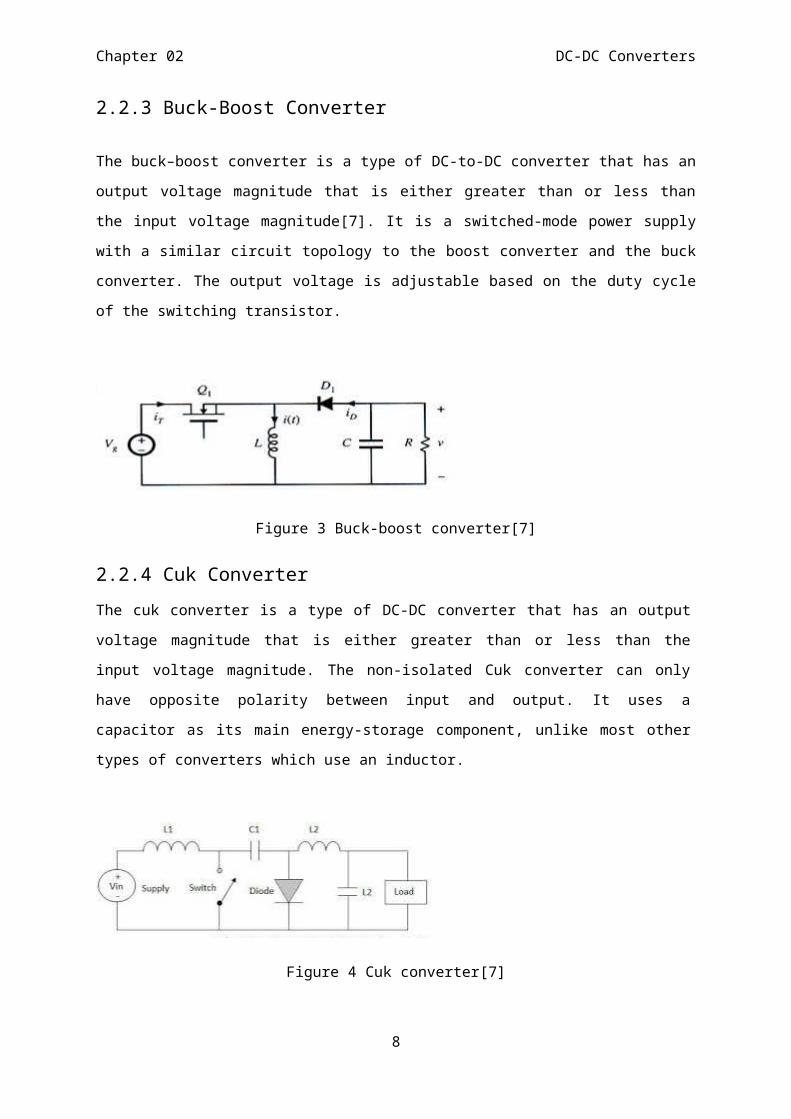
2.2.3 Buck-Boost Converter
The buck–boost converter is a type of DC-to-DC converter that has an output voltage magnitude that
is either greater than or less than the input voltage magnitude[7]. It is a switched-mode power supply
with a similar circuit topology to the boost converter and the buck converter. The output voltage is
adjustable based on the duty cycle of the switching transistor.
Figure 3 Buck-boost converter[7]
2.2.4 Cuk Converter
The cuk converter is a type of DC-DC converter that has an output voltage magnitude that is either
greater than or less than the input voltage magnitude. The non-isolated Cuk converter can only have
opposite polarity between input and output. It uses a capacitor as its main energy-storage component,
unlike most other types of converters which use an inductor.
5

Chapter 02 DC-DC Converters
Figure 4 Cuk converter[7]
2.3 Working Principle of Buck Converter
The buck converter circuit converts a higher dc input voltage to lower dc output voltage. The
basic buck dc-dc converter topology is shown in figure 5[4],[6].
Figure 5 DC-DC buck converter[5]
Figure 6 Operating modes of buck converter[6]
(a) On State (b) Off State
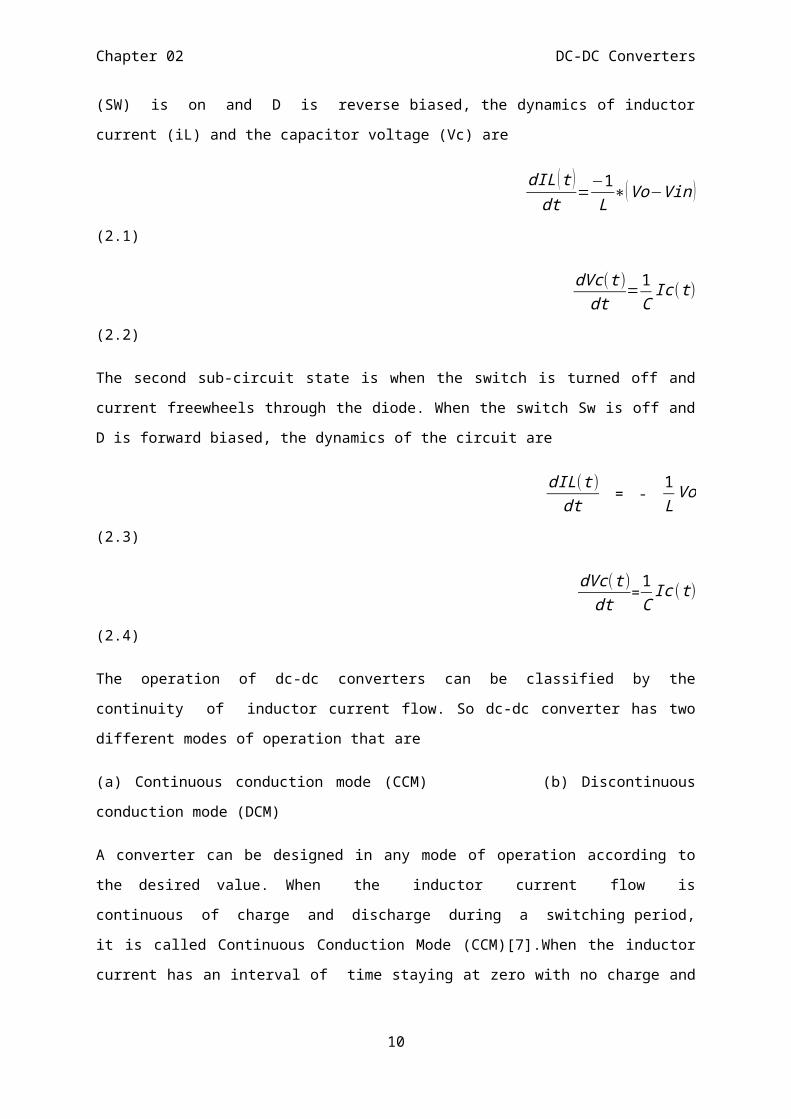
It consists of a controlled switch (SW), an uncontrolled switch (D), an inductor (L), a
capacitor(C), and a load resistance(R). The first sub-circuit state is when the switch is turned on, diode
is reverse biased and inductor current flows through the switch. When the switch (SW) is on
and D is reverse biased, the dynamics of inductor current (iL) and the capacitor voltage (Vc) are
6

Chapter 02 DC-DC Converters
dIL ( t )
dt=−1
L∗(Vo−Vin ) (2.1)
dVc( t)
dt= 1
CIc(t )
(2.2)
The second sub-circuit state is when the switch is turned off and current freewheels through the diode.
When the switch Sw is off and D is forward biased, the dynamics of the circuit are
dIL(t )
dt = -
1L
Vo
(2.3)
dVc( t)
dt=
1C
Ic( t)
(2.4)
The operation of dc-dc converters can be classified by the continuity of inductor current flow.
So dc-dc converter has two different modes of operation that are
(a) Continuous conduction mode (CCM) (b) Discontinuous conduction mode (DCM)
A converter can be designed in any mode of operation according to the desired value. When the
inductor current flow is continuous of charge and discharge during a switching period, it is
called Continuous Conduction Mode (CCM)[7].When the inductor current has an interval of time
staying at zero with no charge and discharge then it is said to be working in Discontinuous
Conduction Mode (DCM) operation and the waveform of inductor current.
2.4 Mathematical Modelling of Buck Converter
The buck converter is introduced as a means of reducing the dc voltage, using only non-dissipative
switches, inductors, and capacitors[8]. The switch produces a rectangular waveform V s( t) as
illustrated in Figure 7.The voltage V s (t )is equal to the dc input voltage V gwhen the switch is in
position 1, and is equal to zero when the switch is in position 2.In practice, the switch is realized using
power semiconductor devices, such as transistors and diodes, which are
7
Chapter 02 DC-DC Converters
controlled to turn on and off as required to perform the function of the ideal switch. The switching
frequency f sequal to the inverse of the switching period T s generally lies in the range of 1 kHz to 1
MHz, depending on the switching speed of the semiconductor devices. The duty ratio D is the fraction
of time that the switch spends in position 1, and is a number between zero and one. The complement
of the duty ratio, D’ is defined as (1 – D).
The switch reduces the dc component of the voltage: the switch output voltage V s (t )has a dc
component that is less than the converter dc input voltage V g . From Fourier analysis, we know that
the dc component of V s ( t ) is given by its average value ⟨ V s ⟩,
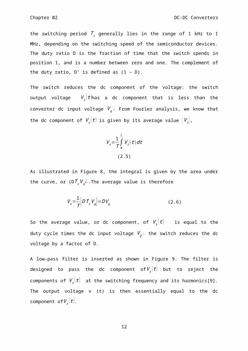
V s=1T ∫
0
T s
V s(t)dt (2.5)
As illustrated in Figure 8, the integral is given by the area under the curve, or (DT s V g ¿ .The average
value is therefore
V s=1T
[ D T sV g ]=D V g (2.6)
So the average value, or dc component, of V s ( t ) is equal to the duty cycle times the dc input voltage
V g . the switch reduces the dc voltage by a factor of D.
8
Figure 7 Ideal switch[9] (a)used to reduce voltage DC component (b) its output voltage waveform Vs(t)
Figure 8 Determination of switch output voltage dc component[9]

Chapter 02 DC-DC Converters
A low-pass filter is inserted as shown in Figure 9. The filter is designed to pass the dc component of
V s ( t ) but to reject the components of V s (t ) at the switching frequency and its harmonics[9]. The
output voltage v (t) is then essentially equal to the dc component ofV s ( t ).
V ≈ V s=D V g
(2.7)
The converter of Figure 7 has been realized using lossless elements. To the extent that they are ideal,
the inductor, capacitor, and switch do not dissipate power. For example, when the switch is closed,
its voltage drop is zero, and the current is zero when the switch is open. In either case, the power
dissipated by the switch is zero. Hence, efficiencies approaching 100% can be obtained. So to the
extent that the components are ideal, we can realize our objective of changing dc voltage levels using
a lossless network.
The network of Figure 9 also allows control of the output. Figure 10 is the control characteristic of the
converter. The output voltage, given by Eq. (2.7), is plotted vs. duty cycle. The buck converter has a
linear control characteristic. Also, the output voltage is less than or equal to the input voltage, since 0
≤ D ≤ 1. Feedback systems are often constructed that adjust the duty cycle D to regulate the converter
9
Figure 9 Insertion of low pass filter to remove the switching harmonics[10]
Figure 10 Buck converter dc output voltage v/s duty cycle[10]

Chapter 02 DC-DC Converters
output voltage. Inverters or power amplifiers can also be built, in which the duty cycle varies slowly
with time and the output voltage follows[10].
2.5 Inductor Volt-Second Balance, Capacitor Charge Balance
Now we analyse the inductor current waveform. We find the inductor current by integrating the
inductor voltage waveform. With the switch in position 1, the left side of the inductor is connected to
the input voltage V g and the circuit reduces to Figure 11(a). The inductor voltageV L ( t ) is then given
by
V L=V g−V (t) (2.8)
As described above, the output voltage v(t) consists of the dc component V, plus a small ac ripple
term V ripple( t) we can make the small ripple approximation here, Eq. (2.8), to replace v (t) with its dc
component V:
V L=V g−V (2.9)
So with the switch in position 1, the inductor voltage is essentially constant and equal to V g−V as
shown in Figure 12. By knowledge of the inductor voltage waveform, the inductor current can be
found by use of the definition
10
Figure 11 Buck converter (a)when switch is in position 1 (b) while the switch in position 2
Figure 12 Steady state inductor voltage waveform of buck converter

Chapter 02 DC-DC Converters
Thus, during the first interval, when is approximately (V g−V ) , the slope of the inductor current
waveform is,
V L (t )=Ld iL( t)
dt (2.10)
d iL(t )
dt=
V L(t)L
=V g−V
L
(2.11)
which follows by dividing Eq. (2.9) by L, and substituting Eq. (2.10). Since the inductor voltage
V L ( t ) is essentially constant while the switch is in position 1, the inductor current slope is also
essentially constant and the inductor current increases linearly. Similar during the second subinterval
when the switch is in position 2. The left side of the inductor is then connected to ground, leading to
the circuit of Figure 11(b). It is important to consistently define the polarities of the inductor current
and voltage; in particular, the polarity of V L (t ) is defined consistently in Figure 11(a), and (b). So the
inductor voltage during the second subinterval is given by,
V L(t )=−V (t)
(2.12)
Use of the small ripple approximation, Eq. (2.12), leads to
V L(t )=−V (2.13)
So the inductor voltage is also essentially constant while the switch is in position 2, as illustrated in
Figure 7. Substitution of Eq. (2.10) into Eq. (2.13) and solution for the slope of the inductor current
yields
d iL(t )
dt=
−V L
L
(2.14)
Hence, during the second subinterval the inductor current changes with a negative and essentially
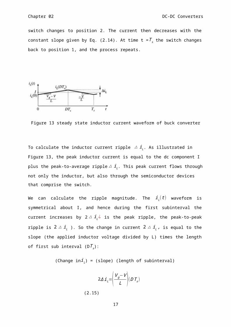
constant slope[9]-[10]. We can now sketch the inductor current waveform as shown in Figure13. The
inductor current begins at some initial valueiL (0). During the first subinterval, with the switch in
position1, the inductor current increases with the slope given in Eq. (2.11). At time t = DT s the
switch changes to position 2. The current then decreases with the constant slope given by Eq. (2.14).
11
Chapter 02 DC-DC Converters
At time t =T s the switch changes back to position 1, and the process repeats.
Figure 13 steady state inductor current waveform of buck converter
To calculate the inductor current ripple iL. As illustrated in Figure 13, the peak inductor current is
equal to the dc component I plus the peak-to-average ripple iL. This peak current flows through not
only the inductor, but also through the semiconductor devices that comprise the switch.
We can calculate the ripple magnitude. The iL (t) waveform is symmetrical about I, and hence during
the first subinterval the current increases by 2 iL¿ is the peak ripple, the peak-to-peak ripple is
2 iL ). So the change in current 2 iL , is equal to the slope (the applied inductor voltage divided
by L) times the length of first sub interval (DT s):
(Change iniL) = (slope) (length of subinterval)
2ΔiL=(V g−V
L )(D T s)
(2.15)
Solution for iL yields
ΔiL=(V g−V
2 L )(D T s)
(2.16)
Typical values of (2 iL) lie in the range of 10% to 20% of the full-load value of the dc component
I. It is undesirable to allow(2 iL) to become too large; doing so would increase the peak currents of
the inductor and of the semiconductor switching devices, and would increase their size and cost. So
by design the inductor current ripple is also usually small compared to the dc component I. The
small-ripple approximation iL (t) = I is usually justified for the inductor current.
12

Chapter 02 DC-DC Converters
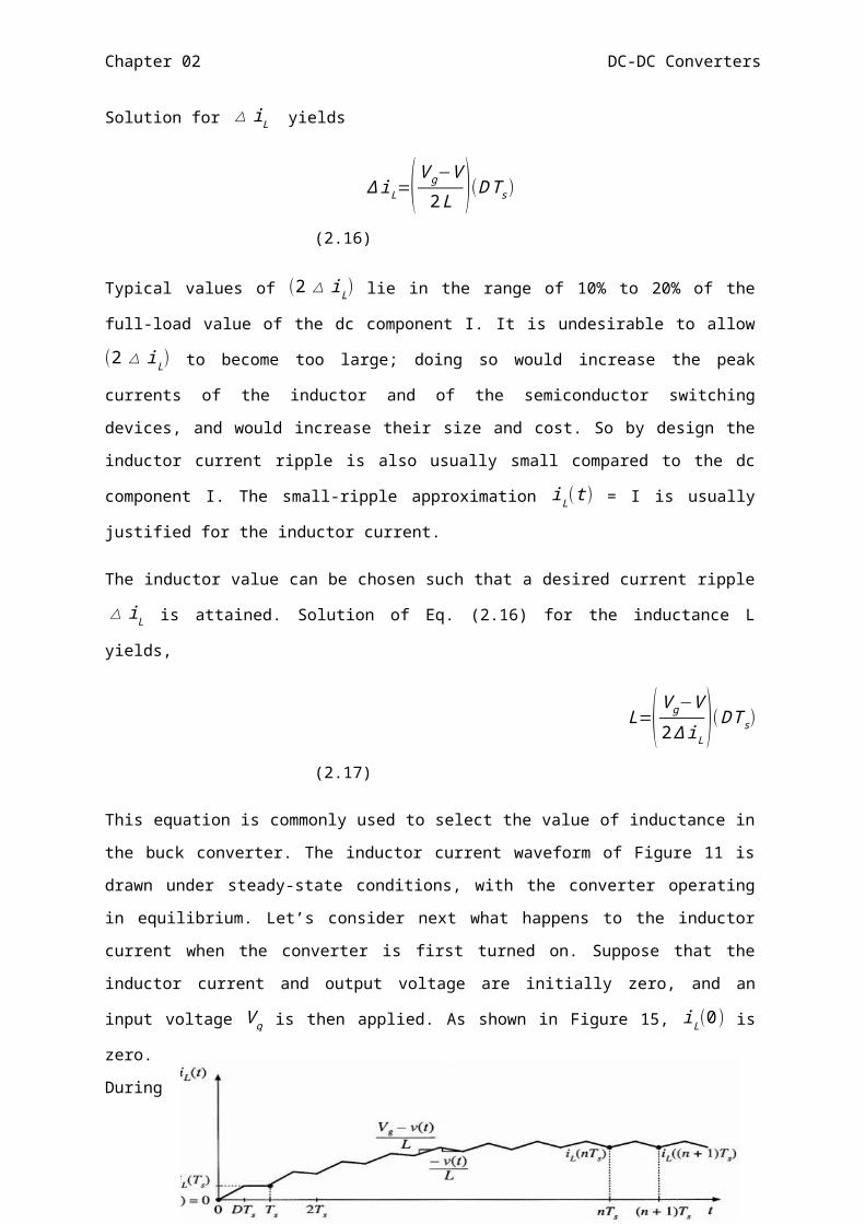
The inductor value can be chosen such that a desired current ripple iL is attained. Solution of Eq.
(2.16) for the inductance L yields,
L=(V g−V
2 ΔiL)(D T s)
(2.17)
This equation is commonly used to select the value of inductance in the buck converter. The inductor
current waveform of Figure 11 is drawn under steady-state conditions, with the converter operating
in equilibrium. Let’s consider next what happens to the inductor current when the converter is first
turned on. Suppose that the inductor current and output voltage are initially zero, and an input
voltage V g is then applied. As shown in Figure 15, iL (0) is zero. During the first subinterval, with
the switch in position 1, we know that the inductor current will increase, with a slope of (V g−V )
L
and with v initially zero. Next, with the switch in position 2, the inductor current will change with a
slope of – V/L; Since V is initially zero, this slope is essentially zero. It can be seen that there is a net
increase in inductor current over the first switching period, because iL T s is greater thaniL (0). Since
the
inductor
current
flows to
the
output,
the
output capacitor will charge slightly, and v will increase slightly. The process repeats during the
second and succeeding switching periods, with the inductor current increasing during each
subinterval 1 and decreasing during each subinterval 2.
As the output capacitor continues to charge and v increases, the slope during subinterval 1 decreases
while the slope during subinterval 2 becomes more negative. Eventually, the point is reached where
the increase in inductor current during subinterval 1 is equal to the decrease in inductor current
during subinterval 2. There is then no net change in inductor current over a complete switching
period, and the converter operates in steady state. The converter waveforms are periodic
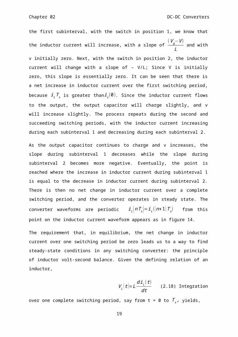
iL ( nT s )=iL ((n+1 ) T s) from this point on the inductor current waveform appears as in figure 14.
The requirement that, in equilibrium, the net change in inductor current over one switching period be
zero leads us to a way to find steady-state conditions in any switching converter: the principle of
13
Figure 14 Inductor current waveform during converter turn on transient
Chapter 02 DC-DC Converters
inductor volt-second balance. Given the defining relation of an inductor,
V L (t )=Ld iL( t)
dt (2.18) Integration over one complete
switching period, say from t = 0 to T s , yields,
iL (T s )−iL (0 )= 1L∫0
T s
V L (t)dt (2.19)
This equation states that the net change in inductor current over one switching period, given by the
left- hand side of Eq. (2.19), is proportional to the integral of the applied inductor voltage over the
interval. In steady state, the initial and final values of the inductor current are equal, and hence the
left-hand side of Eq. (2.19) is zero. Therefore, in steady state the integral of the applied inductor
voltage must be zero:
0=∫0
Ts
V L (t)dt(2.20)
The right-hand side of Eq. (2.20) has the units of volt-seconds or flux-linkages. Eq. (3.20) states that
the total area, or net volt-seconds, under the iL waveform must be zero.An equivalent form is
obtained by dividing both sides of Eq. (2.19) by the switching periodT s ,
0= 1T s∫0
T s
V L( t)dt=⟨V L ⟩ (2.21)
The right hand side of Eq. (2.21) is recognized as the average value, or dc component of iLstates
that, in equilibrium, the applied inductor voltage must have zero dc component.
The inductor voltage waveform of Figure 7 is reproduced in Figure 13, with the area under the V L ( t )
curve specifically identified. The total area λ is given by the areas of the two rectangles,
14
Figure 15 The principle of inductor volt second balance is steady state, the net volt seconds applied to an inductor (i-e he total
area must be λ).

Chapter 02 DC-DC Converters
λ=∫0
Ts
V L ( t )=(V g−V ) ( DT s )+ (−V )(DT s) (2.22)
The average value is therefore
⟨ V L ⟩= λT s
=D (V g−V )+¿D’ (-V) (2.23)
By equating ⟨ V L ⟩to zero, and noting that one obtains
0=DV g−¿) V=DV g−V (2.24)
Solution for V yields
V=DV g
(2.25)
2.6 DC-DC Converters Control
The dc-dc buck converters and the dc-dc boost converter are the simplest power converter
circuits used for many power management and voltage regulator applications[11]. Hence, the
analysis and design of the control structure is done for these basic converter circuits. Voltage-
mode control and Current-mode control are two commonly used control schemes to regulate the
output voltage of dc-dc converters. Both control schemes have been widely used in low-voltage low-
power switch-mode dc-dc converters integrated circuit design in industry. Feedback loop method
automatically maintains a precise output voltage regardless of variation in input voltage and load
conditions. Currently, there exist many different approaches that have been proposed for the
PWM switching control design, e.g., state space averaging methods PID control, optimal control,
sliding mode control and fuzzy control etc. The dc-dc switching converters are the widely used
circuits in electronics systems[12]. They are usually used to obtain a stabilized output voltage
from a given input DC voltage which is lower (buck) from that input voltage, or higher (boost) or
generic (buck–boost). Each of these circuits is basically composed of transistor and diode
making up the switching circuit and inductor and capacitor building the filter circuit. In
addition to these, the circuit may have feedback circuit for the purpose of controlling the output
parameters [11].
15
Chapter 02 DC-DC Converters
The design of buck converters and boost converters with a review over their state space equations led
us to the derivative that the operation of such dc-dc converters is performed through two modes let the
first mode be the on-state and the latter is the off-state depending on the switching circuit . After the
study of the state space model of the converters the basic controlling circuits were implemented
through voltage control, current control, PI and PID control techniques which were best for
steady state analysis[14]. However their performance was questioned for transient analysis. This
motivated the development of several non-linear control techniques for dc-dc converters like sliding
mode control, hysteresis control etc. But the difficulty in implementing their mathematical model
to the physical circuit led to the development of various feedback controllers.
16

Chapter 03 Pulse Width Modulation
Chapter 03
Pulse Width Modulation
3.1 Pulse Width Modulation
A PWM circuit works by making a pulsating DC square wave with a variable on-to-off ratio. The
average on time may be varied from 0 to 100 percent. In this way, a variable amount of power is
transferred to the load. The main advantage of a PWM circuit over a resistive power controller is the
efficiency.
The average value of voltage (and current) fed to the load is controlled by turning the switch between
supply and load on and off at a fast pace. The longer the switch is on compared to the off periods, the
higher the power supplied to the load is. The PWM switching frequency has to be much faster than
what would affect the load, which is to say the device that uses the power.
3.1.1 Duty Cycle
The term duty cycle describes the proportion of 'on' time to the regular interval or 'period' of time; a
low duty cycle corresponds to low power, because the power is off for most of the time. Duty cycle
is expressed in percent, 100% being fully on.
D =t s
Ton
(3.1)
17
Figure 16 Pulse Width Modulator

Chapter 03 Pulse Width Modulation
3.1.2 Advantages of PWM
The main advantage of PWM is that power loss in the switching devices is very low. When a switch
is off there is practically no current, and when it is on, there is almost no voltage drop across the
switch. Power loss, being the product of voltage and current, is thus in both cases close to zero.
PWM also works well with digital controls, which, because of their on/off nature, can easily set the
needed duty cycle. PWM has also been used in certain communication systems where its duty cycle
has been used to convey information over a communications channel.
3.1.3 PWM Controller
The heart of a switching power supply is its switch control circuit (controller). The key objective in
designing a controller for the power converter is to obtain tight output voltage regulation under
different line and load conditions. The control circuit is a negative-feedback control loop connected
to the switch through a comparator and a Pulse Width Modulator (PWM). The switch control
regulates the output voltage against changes in the load and the input voltage.
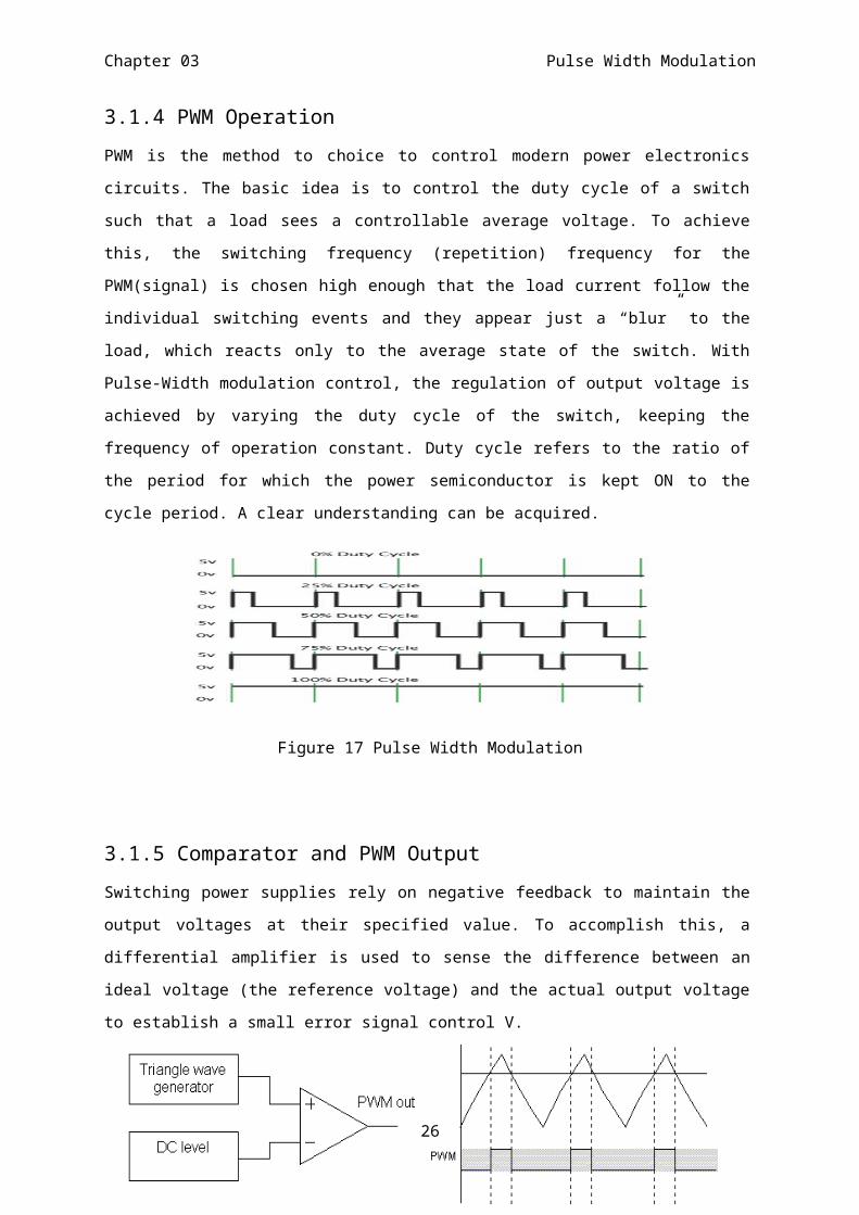
3.1.4 PWM Operation
PWM is the method to choice to control modern power electronics circuits. The basic idea is to
control the duty cycle of a switch such that a load sees a controllable average voltage. To achieve
this, the switching frequency (repetition) frequency for the PWM(signal) is chosen high enough that
the load current follow the individual switching events and they appear just a “blur” to the load,
which reacts only to the average state of the switch. With Pulse-Width modulation control, the
regulation of output voltage is achieved by varying the duty cycle of the switch, keeping the
frequency of operation constant. Duty cycle refers to the ratio of the period for which the power
semiconductor is kept ON to the cycle period. A clear understanding can be acquired.
Figure 17 Pulse Width Modulation
3.1.5 Comparator and PWM Output
Switching power supplies rely on negative feedback to maintain the output voltages at their specified
18
Chapter 03 Pulse Width Modulation
value. To accomplish this, a differential amplifier is used to sense the difference between an ideal
voltage (the reference voltage) and the actual output voltage to establish a small error signal control
V.
The PWM switching at a constant at a constant switching frequency is generated by comparing a
signal-level control voltage control v with a repetitive waveform as shown in figure 18.
The frequency of the repetitive waveform with a constant peak which is shown to be a saw- tooth,
establishes the switching frequency. This frequency is kept constant in a PWM control and is chosen
to be in a few hundred kilohertz range. When the amplified error signal, which varies very slowly
with time relative to the switching frequency, is greater than the saw tooth waveform, the switch is
off. So when the circuit output voltage changes, control V also changes causes the comparator
threshold so changes consequently, the output pulse width also changes. This duty cycle change then
moves the output voltage to reduce to error signal to zero, thus completing the control loop.
3.2 Control Technique
3.2.1 PID Controller
A proportional-integral-derivative controller (PID controller) is a generic control loop feedback
mechanism widely used in industrial control systems. A PID controller attempts to correct the error
between a measured process variable and a desired set point. The PID controller calculation
(algorithm) involves three separate parameters; the Proportional, the Integral and Derivative
values[16]. The Proportional value determines the reaction to the current error, the Integral
determines the reaction based on the sum of recent errors and the Derivative determines the
reaction to the rate at which the error has been changing. The weighted sum of these three
actions is used to adjust the process via a control element such as the position of a control valve or the
power supply of a heating element. By "tuning" the three constants in the PID controller
algorithm the PID can provide control action designed for specific process requirements[14]-
[15]. The response of the controller can be described in terms of the responsiveness of the controller
19
Figure 18 Comparator output

Chapter 03 Pulse Width Modulation
to an error, the degree to which the controller overshoots the set-point and the degree of system
oscillation. Note that the use of the PID algorithm for control does not guarantee optimal control of
the system.
(a) Proportional Term
The proportional term makes a change to the output that is proportional to the current error value. The
proportional response can be adjusted by multiplying the error by a constant Kp, called the
proportional gain. The proportional term is given by:
Pout=Kpe (t) (3.2)
Where
Pout: Proportional output
Kp: Proportional Gain, a tuning parameter
e: Error = SP − PV
t:Time or instantaneous time (the present)
A high proportional gain results in a large change in the output for a given change in the error. If the
proportional gain is too high, the system can become unstable (See the section on Loop Tuning). In
contrast, a small gain results in a small output response to a large input error, and a less responsive (or
sensitive) controller. If the proportional gain is too low, the control action may be too small when
responding to system disturbances. In the absence of disturbances pure proportional control will
not settle at its target value, but will retain a steady state error that is a function of the
proportional gain and the process gain. Despite the steady-state offset, both tuning theory and
industrial practice indicate that it is the proportional term that should contribute the bulk of the
output change.
(b) Integral Term
The contribution from the integral term is proportional to both the magnitude of the error and the
duration of the error. Summing the instantaneous error over time (integrating the error) gives the
accumulated offset that should have been corrected previously[15]. The accumulated error is
then multiplied by the integral gain and added to the controller output. The magnitude of the
contribution of the integral term to the overall control action is determined by the integral gain,
Ki.
The integral term is given by:
20
Chapter 03 Pulse Width Modulation
Iout=Ki∫0
t
e (τ ) d τ (3.3)
Where
Iout: Integral output
Ki: Integral Gain, a tuning parameter
Error = SP − PV
τ: Time in the past contributing to the integral response
The integral term (when added to the proportional term) accelerates the movement of the process
towards set point and eliminates the residual steady-state error that occurs with a proportional only
controller. However, since the integral term is responding to accumulated errors from the past, it can
cause the present value to overshoot the set point value (cross over the set point and then create a
deviation in the other direction)[17]. For further notes regarding integral gain tuning and controller
stability, see the section on Loop Tuning.
(c) Derivative Term
The rate of change of the process error is calculated by determining the slope of the error over time
(i.e. its first derivative with respect to time) and multiplying this rate of change by the
derivative gain Kd. The magnitude of the contribution of the derivative term to the overall control
action is determined the
Dout=Kddedt
(3.4)
Where
Dout: Derivative output
Kd: Derivative Gain, a tuning parameter
e: Error = SP − PV
t: Time or instantaneous time (the present)
The derivative term slows the rate of change of the controller output and this effect is most noticeable
close to the controller set point. Hence, derivative control is used to reduce the magnitude of the
overshoot produced by the integral component and improve the combined controller-process
stability. However, differentiation of a signal amplifies noise in the signal and thus this term in the
21
Chapter 03 Pulse Width Modulation
controller is highly sensitive to noise in the error term, and can cause a process to become unstable if
the noise and the derivative gain are sufficiently large. The output from the three terms, the
proportional, the integral and the derivative terms are summed to calculate the output of the PID
controller.
First estimation is the equivalent of the proportional action of a PID controller. The integral action of
a PID controller can be thought of as gradually adjusting the output when it is almost right. Derivative
action can be thought of as making smaller and smaller changes as one gets close to the right level and
stopping when it is just right, rather than going too far[16]-[18]. Making a change that is too large
when the error is small is equivalent to a high gain controller and will lead to overshoot. If the
controller were to repeatedly make changes That were too large and repeatedly overshoot the
target, this control loop would be termed unstable and the output would oscillate around the set
point in a either a constant, a growing or a decaying sinusoid. A human would not do this
because we are adaptive controllers, learning from the process history, but PID controllers do
not have the ability to learn and must be set up correctly. Selecting the correct gains for effective
control is known as tuning the controller.
If a controller starts from a stable state at zero error (PV = SP), then further changes by the controller
will be in response to changes in other measured or unmeasured inputs to the process that impact on
the process, and hence on the PV. Variables that impact on the process other than the MV are known
as disturbances and generally controllers are used to reject disturbances and/or implement set point
changes. In theory, a controller can be used to control any process which has a measurable
output (PV), a known ideal value for that output (SP) and an input to the process (MV) that will affect
the relevant PV. Controllers are used in industry to regulate temperature, pressure, flow rate, chemical
composition, level in a tank containing fluid, speed and practically every other variable for which a
measurement exists. Automobile cruise control is an example of a process outside of industry which
utilizes automated control. Kp: Proportional Gain - Larger Kp typically means faster response since
the larger the error, the larger the feedback to compensate. An excessively large proportional
gain will lead to process instability. Ki: Integral Gain - Larger Ki implies steady state errors are
eliminated quicker. The trade-off is larger overshoot: any negative error integrated during transient
response must be integrated away by positive error before we reach steady state. Kd: Derivative Gain
- Larger Kd decreases overshoot, but slows down transient response and may lead to instability.
(d) Loop Tuning
If the PID controller parameters (the gains of the proportional, integral and derivative terms) are
chosen incorrectly, the controlled process input can be unstable, i.e. its output diverges, with
or without oscillation, and is limited only by saturation or mechanical breakage. Tuning a
22
Chapter 03 Pulse Width Modulation
control loop is the adjustment of its control parameters (gain/proportional band, integral gain/reset,
derivative gain/rate) to the optimum values for the desired control response.
Some processes must not allow an overshoot of the process variable beyond the set point if, for
example, this would be unsafe. Other processes must minimize the energy expended in reaching
a new set point. Generally, stability of response (the reverse of instability) is required and the
process must not oscillate for any conditions or set points.
Some processes have a degree of non-linearity and so parameters that work well at full-load
conditions don't work when the process is starting up from no-load. This section describes some
traditional manual methods for loop tuning[18].
There are several methods for tuning a PID loop. The most effective methods generally involve the
development of some form of process model, and then choosing P, I, and D based on the dynamic
model parameters. Manual "tune by feel" methods have proven time and again to be inefficient,
inaccurate, and often dangerous.
In the control of dynamic systems, no controller has enjoyed both the success and the failure of the
PID control. Of all control design techniques, the PID controller is the most widely used. Over 85% of
all dynamic controllers are of the PID variety. There is actually a great variety of types and design
methods for the PID controller.
In this project we are using PI controller to control the speed of dc motor. We left the D controller
because in our simulation there is no overshoot.
3.3 Transfer Function of Buck Converter
When the switch is in position 1 as shown in fig 19, the circuit is in on state,
Figure 19 Buck converter
23

Chapter 03 Pulse Width Modulation
For on state:
didt
=V ¿
L−
V o
L
d V c
dt=
ic
C−
V o
RC
When the switch is in position 2, the circuit is in off state,
For off state:
didt
=−V c
L
d V c
dt=
ic
C−
V o
RC
State space equation is:
TF=¿ [ 0−1L
1C
−1RC
] [ iv ]+ [ 1
L0 ]V ¿
From above equation,
A=[ 0−1L
1C
−1RC
] B = [ 1
L0 ]
C = [ 0 1 ] [ iv ]
TF = C[s I – A]−1 B
Putting values of A, B, C in above equation,
24

Chapter 03 Pulse Width Modulation
TF = [ 0 1 ] [s [1 00 1]−[ 0
−1L
1C
−1RC
]]−1
[ 1L0 ]
TF = [ 0 1 ]¿¿
¿¿
TF = [ 0 1 ]¿¿
The transfer function is,
TF =
1LC
s2+s
RC+
1LC
(3.5)
3.4 Conclusion
The averaged modelling approach for the switching mode converter leads to an approximate nonlinear
models. The linearization of this kind of models around the operating point allows the application of
conventional control approach such as PID control and adaptive control.
25

Chapter 04 Simulation Results
Chapter 04
Simulation ResultsThis chapter describes the procedure of mathematical modelling of buck convertor using Simulink
tool of MATLAB. First step of this procedure involve the simulation of buck converter using resistive
load and the simulation using resistive and inductive load. The output voltage of buck converter does
not meet the required level[19]. In order to get the voltage at the required level we used a feedback
method of PID controller and PWM technique. This procedure work on the base of duty ratio depends
on the ratio of output to input voltage. We set the reference level which produces the difference in
output and reference voltage and produces a Proportional, integral and differential gain and give the
input to PWM which produces a waveform of require duty ratio and switches the MOSFET and
required results are obtained.
4.1 SIMULINK Model for Buck Converter
26
VgR
CDC SOURCE
MOSFET
DIODE
L
9
input power2
8
outputpower1
7
diode volt
6
diode current
5
capacitor current
4
output voltage
3
load current
2
inductor current
1
input current1
outputpoweroutput power
input power1
input power
v+-
v+-
v+-
RESULTS1
PWM out put
0
Multimeter
g m
D S
i+
-
Current3
i+ -
Current2
i+
-
Current 3
i+ -
Current 1
i+ -
Current
1
pwm input
Figure 20 Simulink model of buck converter

Chapter 04 Simulation Results
The design procedure of buck convertor in MATLAB is shown in figure 20.It follows that diode,
inductor, capacitor and load resistor all are connected in parallel. MOSFET is connected to the voltage
source. The PWM output is applied to the MOSFET gate terminal in order to give a feedback of the
load to buck converter. The scope at the end show the graphical results.
4.2 Simulation with PI Controller
4.2.1 SIMULINK Diagram of Buck Converter with PI Controller
27
input current
inductor current
load current
load voltage
capacitor current
Po
Pi
Id
Vd
PID output
Close Loop BUCK CONVERTER
Continuous
powergui
Duty Ratio input
input current1
inductor current
load current
output v oltage
capacitor current
diode current
diode v oltage1
outputpower1
input power2
open loop BUCK CONVERTER
5 Vr
vd
To Workspace9
id
To Workspace8
Pi
To Workspace7
Po
To Workspace6
Ic
To Workspace5
IL
To Workspace4
Iin
To Workspace3
i
To Workspace2
dr
To Workspace10
clk
To Workspace1
vo
To Workspace
RESULTS1
RESULTS
Duty ratio pwm out
PWM1
Duty ratio pwm out
PWM
pwm input
input current1
inductor current
load current
output voltage
capacitor current
diode current
diode volt
outputpower1
input power2
PID(s)
PID Controller
1s
Integrator
-K-
Gain
.5
Duty ratio
Clock
Figure 21 SIMULINK model of open and close loop buck converter
Chapter 04 Simulation Results
This is complete MATLAB model of open and close loop buck convertor model. The open loop test is
for verification of output voltages without feedback to the controller. The waveform in case of open
loop does not correctly match to the desired voltage waveform. Hence the design consideration does
not approve. In close loop gain the output voltage meet correctly with the reference voltage. In case of
change in output voltage due to the load change, the compensator takes the difference of two values
and give to the PID controller which generates the proportional, integral and differential gain. The
output of the PID controller feed to the PWM which generates the waveform of require duty cycle and
output of PWM then fed to MOSFET for switching as shown in figure 21.
4.2.2 SIMULINK Diagram of PWM
Many industrial applications use Pulse Width Modulation (PWM) signals because such signals are
robust in the presence of noise. Figure 22 shows two PWM signals. In the top plot, a PWM signal
with a 20% duty cycle represents a 0.2 V DC signal. A 20% duty cycle corresponding to 1 V signal
for 20% of the cycle, followed by a value of 0 V signal for 80% of the cycle. The average signal value
is 0.2 V. When linearizing a model containing PWM signals there are two effects of linearization you
should consider:
The signal level at the operating point is one of the discrete values within the PWM signal,
not the DC signal value. For example, in the model above, the signal level is either 0 or 1, not
0.8. This change in operating point affects the linearized model.
The creation of the PWM signal within the subsystem voltage to PWM as in figure 22,
compare to zero block. Such comparator blocks do not linearize well due to their
discontinuities and the non-double outputs.
Figure 22 SIMULINK diagram of
PWM
28
1
pwm out
saw tooth generator
ZCD
PWM Details
1
Duty ratio
duty ratio + saw tooth
100khz
100khz
Ki
1
duty ratio
8
Kp
1s
Integrator
17.6
1
error
Chapter 04 Simulation Results
Figure 23 Gain of PI controller
Figure 24 Duty ratio
4.3 Simulation with R-Load
4.3.1 SIMULINK Model of Buck Converter(R-Load)
Figure 25 SIMULATION of buck converter with R-load
29
Chapter 04 Simulation Results
A proportional-integral-derivative controller (PID controller) is a control loop feedback
mechanism (controller) widely used in industrial control system. A PID controller calculates
an error value as the difference between a measured process variable and a desired set point. The
controller attempts to minimize the error by adjusting the process through use of a manipulated
variable.
The PID controller algorithm involves three separate constant parameters, and is accordingly
sometimes called three-term control: the proportional, the integral and derivative values,
denoted P, I, and D. Simply put, these values can be interpreted in terms of time: P depends on
the present error, I on the accumulation of past errors, and D is a prediction of future errors, based on
current rate of change. The weighted sum of these three actions is used to adjust the process.
4.3.2 Results with R-Load
4.3.3 Output Voltage
Figure 26 Output voltage using PI controller
This waveform represents the open and close loop voltage results of buck converter. When buck
convertor is modelled with no feedback/open loop then the voltage lags behind the reference voltage,
contrary the close loop buck converter meet the output voltages with the reference value. In figure 26
blue curve represent the close loop buck converter, as can be seen it is approx. reaches the reference
(green line) set value.
30
0 0.02 0.04 0.06 0.08 0.1 0.12 0.14 0.16 0.18 0.20
1
2
3
4
5
6
Time(sec)
Vol
tage
(V)
Output Voltage
Close Loop
ReferenceOpen Loop

0 0.02 0.04 0.06 0.08 0.1 0.12 0.14 0.16 0.18 0.20
1
2
3
4
5
6
Time(sec)
Current(A
mp)
Inductor Current
Close Loop
Reference
Open Loop
Chapter 04 Simulation Results
4.3.4 Inductor Current
Figure 27 Inductor current using PI controller
This technique represents the working algorithm of open loop and close loop buck with PID
controller. The results obtained in case of open loop are not accurate because the current waveform
does not meet the reference level. When close loop procedure is applied with PID controller then the
output almost perfect and meet the required level. In figure 27 when buck convertor is modelled with
no feedback/open loop then the voltage lags behind the reference current, contrary the close loop buck
converter meet the output current with the reference value. In figure 27 blue curve represent the close
loop buck converter, as can be seen it is approx. reaches the reference (green line) set value.
4.3.5 Capacitor Current
The results obtained in close loop gain show that the capacitor charging time and discharging time are
better while of open loop gain as it linearly decreases to the required value as shown in figure 28.
Figure 28 Capacitor current
31
0 0.05 0.1 0.15 0.2 0.25 0.3-2
0
2
4
6
8
10
12
14x 10
-3
time
curr
ent
(am
p)
capacitor current
close loop
open loop

Chapter 04 Simulation Results
4.4 Simulation with RL-Load
Figure 30 PI
controller for RL-Load
4.4.1 Output
Voltage
32
VgR
CDC SOURCE
MOSFET
DIODE
L
9
input power2
8
outputpower1
7
diode volt
6
diode current
5
capacitor current
4
output voltage
3
load current
2
inductor current
1
input current1
outputpoweroutput power
input power1
input power
v+-
v+-
v+-
RESULTS1
PWM out put
0
Multimeter
g m
D S
i+
-
Current3
i+ -
Current2
i+
-
Current 3
i+ -
Current 1
i+ -
Current
1
pwm input
Ki
1
duty ratio
24
Kp
1s
Integrator
17.6
1
error
0 0.02 0.04 0.06 0.08 0.1 0.12 0.14 0.16 0.18 0.20
1
2
3
4
5
6
time
volta
ge (v
olts)
output voltage
close loop
open loopreference
Figure 29 SIMULINK model of buck converter with RL-load
Chapter 04 Simulation Results
This waveform represents the analysis of buck convertor simulation using the resistive and inductive
load. As obvious that the buck convertor is a device which step down the voltage and step up the
current in voltage controlled mode. The green line in this figure the response of open loop buck
convertor and blue line represents the output of close loop gain indication of better result and shows
that it meet the reference level if we set it at 5V.
4.4.2 Inductor Current
This
figure
represents the response of buck convertor in open loop and close loop. In case of close loop gain the
results meet
the required level but in case of open loop gain the response of output voltage does not meet the
reference level.
4.4.3 Capacitor Current
33
0 0.02 0.04 0.06 0.08 0.1 0.12 0.14 0.16 0.18 0.20
1
2
3
4
5
6output current
time
curre
nt (a
mp)
close loop
open loopreference
0 0.01 0.02 0.03 0.04 0.05 0.06 0.07-0.2
-0.1
0
0.1
0.2
0.3
time
curre
nt (
amp)
capacitor current
close loop
open loop
Figure 32 Output Current using PI controller for RL-load
Figure 33 Capacitor Current using PI controller for RL-load
Chapter 04 Simulation Results
This waveform represents the response of capacitor in both open loop and close loop gain. In case of
open loop the response is not decaying rapidly as compare to the close loop gain. The function of the
output capacitor is to filter the inductor current ripple and deliver a stable output voltage. It also has to
ensure that load steps at the output can be supported before the regulator is able to react.
4.5 Simulation of Project on Proteus
Simulation of our project is done on Proteus7.6 SP0 full software. All the components are placed
according to the circuit diagram as shown in the circuit diagram.
4.5.1 Working Procedure
As basic supply is 230VAC, so it is stepped down to 20VAC by transformer. Then 20VAC is
converted to 20VDC by full bridge circuit, this voltage is full of ripples, to remove ripples filter
circuit is designed. At the end of filter circuit ripples free 20VDC is obtained. This DC voltage is
given to the buck converter circuit as input voltage, the buck converter step down this voltage to
12VDC. At the output of buck converter a gear motor is put as a load.
The output of buck converter is fed back to PIC microcontroller(PIC16F877A) to adjust the duty ratio
accordingly to our set value 12VDC. PIC microcontroller use PID controller algorithm to set the duty
ratio and to generate the PWM accordingly.
This PWM output from PIC microcontroller is fed to Gate terminal of IRF 540.The MOSFET
switches depending upon the duty ratio, to set the voltage to a set point. In this way the output of buck
converter is regulated. If the load is varied, the loop will automatically maintain the output voltage.
Three parameters like output voltage, rpm and duty ratio are displayed on LCD.
The simulation model is shown in Figure 34 .
34

Chapter 04 Simulation Results
Figure 34 Simulation diagram on Proteus
4.6 Conclusion
The results of PI controller are satisfactory, so we implemented PI controller algorithm for
buck converter in SIMULINK.
The simulation results obtained on Proteus are according to the hardware project results.
35

Chapter 05 Hardware Implementation
Chapter 05
Hardware Implementation
5.1 Design Concept
The project design constraints on power efficiency, lower cost, and less reduce space and components
used. For higher power application, power supplies that need to provide higher current not
suitable use to the chip since the current is too high for handled and it might cause IC
damage. And therefore it may cause instability condition when the load or input voltage changing
may cause system at risk. Dynamic power losses are due to the switching behaviour of the
selected pass devices (MOSFETs, Power Transistors, IGBTs, etc.). These losses include turn-on and
turn-off switching losses and switch transition losses. Since an increasing of power electronics circuits
in many applications such used in automobiles to laptops which use an integrated circuit (IC) and
form in smaller size. The lower system cost improvement of power supply show in designing of
power supplies using analogue techniques requires components to be oversized to compensate for
component variation and component drift. Using analogue circuitry to implement system control
functions is not always cost-effective or flexible. Losses in an electric or power electronics circuits
come from many source, in this project the losses such a resistive losses in the controllable switch,
capacitive losses due to charging of the controllable gates and parasitic capacitances, short
circuit current through the controllable switch especially current flow during switch open and
voltage drop across when switch is closed and the parasitic losses of filter in an inductor and
capacitor. More that, in order to regulate the output voltage, the duty cycle to the buck
converter is set by a feedback control loop, but to associate the controller design to buck
converter power elements, it may cause inefficient in power conversion[15]. To ensure the
system stability and for improving transient output response, the more complex proportional integral
derivative (PID) controller can be implemented[17].
5.2 Components Review
5.2.1 Bridge Rectifier
In order to produces unregulated dc supply voltage up to 20Vdc from main supply of 230Vac, this
silicon bridge rectifier is used to the circuit. The cost of this component is cheap with the features
maximum average forward output current.
36

Chapter 05 Hardware Implementation
5.2.2 MOSFET
SMPS MOSFET has limitations operation in terms of voltage, current and power dissipation.
The power absorbed by the gate drive circuitry should not significantly affect the overall efficiency.
The power MOSFET current rating is related with the heat dissipated in the devices. This rating will
be take in consideration for designing appropriate circuit to protect power MOSFET against high
voltage and current, thus cause heat generation. While considering protection of power MOSFET
against over voltage, a distinction has to be made between slowly varying over voltage and short time
surge. It is about 100Vdc the minimum rating of drain to source breakdown voltage. Gate voltage
must be 10-25V higher than the drain voltage. Being a high side switch, such gate voltage would have
to be higher than the rail voltage, which is frequently the higher voltage available in the system. The
data sheet is given in the appendix B.
Figure 35 Pin configuration of IRF 540
5.2.3 Capacitor
The capacitor is chosen with minimum loss because switched power regulators are usually
used in high current-performance power supplies. Loss occurs because of its internal series resistance
and inductance. Commonly capacitors for switched regulators are chosen based on the equivalent
series resistance (ESR). The capacitance of the capacitor (C) is given by
C= 1-D/16Lf^2 (5.1)
5.2.4 Inductor
The function on inductor is to store energy and the value is selected to maintain a continuous
current mode (CCM) operation as a rated of load (5 Ω) is decided for this Buck converter. In CCM,
current flow continuously in inductor during the entire switching cycle and output inductance selected
to limit the peak to peak ripple current flowing. The factors to be considered in selecting the inductor
37

Chapter 05 Hardware Implementation
are its peak to peak ripple current (CCM), maximum dc or peak current (not overheat) and maximum
operating frequency (maximum core loss is not exceeded, resulting in overheating or saturation).
The inductance of the inductor (L) is given by
L=(1-k)R/2f (5.2)
5.2.5 PIC Microcontroller
The microcontroller selected to control the closed –loop feedback conversion power was the 40-pin
PDPIP package of the PIC16F877A. The pin configuration is given in Figure 36. A primary benefit
of this microcontroller is the flexibility of the many I/O pins to accommodate analogue to
digital signals other than easy to firm the program[19].
Figure 36 Pin configuration of PIC16F877A[19]
5.3 PID Based Microcontroller
This Buck system is closed loop feedback system, in order to simulate or to firm the program for
controller, the basic such Proportional Error Gain (P-Gain) which this parameter produces a
correction factor that is proportional to the magnitude of the output voltage error, an integral error
gain (I-Gain) which this parameter uses the cumulative voltage error to generate a correction
38

Chapter 05 Hardware Implementation
factor that eliminates any residual error due to limitations in offset voltages and measurement
resolution an Derivative error gain (D-Gain) which this parameters produces a correction factor
that is proportional to the rate of change of the output error voltage, which helps the system respond
quickly to changes in the system conditions. Feed forward gain, this parameter produces a correction
factor that is computed based on the magnitude of the input voltage, inductor current and circuit
attributes such an inductor and capacitor value. This term allow the control loop to be protective
rather than reactive. In other words, when the input voltage changes, feed forward gain responds so
that the control loop does not have to wait until the output voltage changes before making the
appropriate gain correction. Using the PID algorithm, the proportional, integral and derivative
error of the actual versus the desired output voltage is combined to control the PWM duty cycle. The
PID algorithm will be used in voltage mode control loops[16]. The PID software is typically small,
but its execution rate is very high, often hundreds of thousands of iterations per second. This high
iteration rate requires the PID software routine be as efficient as possible to minimize
performance. The PID control-loop is interrupt-driven by the ADC on a fixed-time basis. Any system
function that can be executed in the “idle loop” should be, in order to reduce the unnecessary
workload within the PID control software. Functions such as voltage ramp up/down, error
detection, feed-forward calculations and communication support routines are candidates for the idle
loop. Any other interrupt-driven processes, such as communication, must beat lower priority than the
PID loop.
5.3.1 Voltage –Mode Control
Voltage-mode control is the methods of control based on analogue switch-mode power supply
(SMPS) control techniques. In voltage mode, the difference between desired and actual output voltage
(error) controls the time that the supply voltage is applied across the inductor, which indirectly
controls current flow in the inductor. Varying the duty cycle essentially adjusts the input voltage drive
to the Buck's LC components which directly effects. Voltage-mode can provide more stability in a
noisy environment and over a wide operating range.
5.4 PIC Microcontroller Tools Development
5.4.1Picbasic Pro Compiler (pbp)
P CBAS C PRO™ Compiler is the easiest way to program the fast and powerful Microchip
Technology PIC microcontrollers (PIC16F877A). PICBASIC PRO converts BASIC programs into
files that can be programmed directly into a PIC MCU. The BASIC language is much easier to read
and write than the quirky Microchip assembly language. PBP compiler produces code that may be
programmed into a wide variety of PIC microcontroller having from 8 up to 84 pins and various on-
chip features including A/D converters, hardware timers and serial ports. The PIC16F877A use
39

Chapter 05 Hardware Implementation
Harvard technology to allow rapid erasing and reprogramming for program debugging. The
PIC16F877A devices also contain between 64 and 1024 bytes of non-volatile data memory that can be
used to store program and data and other parameters even when the power is turned off.
5.5 Methodology
This chapter explains about hardware development such as equipment, procedures and method design
for Buck converter including controller technique used in closed-loop feedback system. Before
looking at the details of all methods below, it is good to begin with brief review of the problem that is
considered in this Buck converter. The changing of voltage from input supply will be consider as
problem need to against by apply feedback controller in order to maintain an output from Buck
converter.
5.5.1 Hardware Development
The hardware development flow diagram consist of the following steps as shown in figure 37.
Figure 37 Design flow for microcontroller based buck converter PID system
In the hardware part, the circuit is design to step down dc – to – dc voltage. The circuit included parts
of Buck components such as controllable switch (IRF540), inductor and capacitor,
PIC16F877Amicrocontroller, and other basic components. Rectifier and filter circuit is design to
obtain voltage up to 20Vdc from main source. The voltage obtained will be step down by Buck
converter to 12Vdc. In order to maintain output voltage, controller will be operated in feedback
circuit. PIC16F877A is used to control SMPSMOSFET switching duty cycle which is connected to
Buck converter circuit. PIC16F877Ahas 40 pins. Since the PWM that will be apply to Buck converter
is varied in order to maintain the output voltage, the HPWM function pin at RC2/CCP1/P1A need to
set in order to generate the PWM signal from the microcontroller. The 10MHz crystal oscillator is
used for PIC16F877A microcontroller internal clock.
5.6 Hardware Module at a Glance
Following figure shows the complete module of project.
40
Chapter 05 Hardware Implementation
Figure 38 Hardware of Project
41
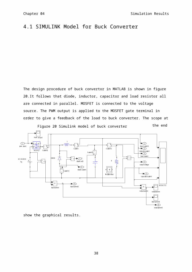
Chapter 06 Conclusion and Future Recommendations
Chapter 06
Conclusion and Future Recommendations
6.1 Conclusion
The time response analysis of the dc-dc buck converter are done by observing their damping nature of
oscillatory transient signals mainly the output voltage in terms of various parameters like time
required to settle to a steady state desired value from the initial high transient values, the maximum
value that the output voltage attains during the transient period and the duration after which the
desired output value is reached for the first time. These objectives are satisfied by observing the rise
time, settling time and overshoot from the graphical results obtained from the simulation. It is seen
that the SMPID controller meets our demand of controlling the output voltage of dc-dc buck converter
in an efficient manner. The implementation of SMPID controller also reduces the unwanted peak of
output voltage during the transient period almost to zero and therefore reduces the chances of
damage , due to sudden rise of voltage in modern day power electronic devices that have a very
narrow tolerance zone to meet the requirements in ultrafast way.
6.2 Future Recommendations
Protection circuits are integral part of the converter system to protect the load from application of high
voltage in case of failure in converter. Over-voltage and over current protection could be added to the
hardware circuit. As we implement the PID controller algorithm in PIC microcontroller to control the
hardware. So the future for this project is to control the hardware form sliding mode controller on
simulation. As we know that the sliding mode controller is more efficient than PID controller.
42

Biblography
References[1] C.Dey and R.K.Mudi ,"An improved auto-tuning scheme for PID controllers,"in ISA
Transactions,vol.48,pp. 396-402, 2009.
[2] K. J.A°stro¨m and T. Hagglund ,"The feature of PID control" Control engineering practice, vol.9,
No.11,pp.1163-75, Nov.2001
[3] M. H. Rashid, “Power Electronics, Circuits, Devices And Applications,” 2 nd ed. Englewood
Cliffs, NJ: Prentice Hall, 1993.
[4] R. W. Erickson and D. Maksimovic,” Fundamentals of Power Electronics”. Norwell, MA:
Kluwer, 2001.
[5] R. P. Severns and G. Bloom ,” Modern dc-to-dc switch-mode power converter circuits”,
1985 :Van Nostrand
[6] R. W. Erickson, “Fundamentals of Power Electronics” Norwell, MA: Kluwer-Academic.1999
[7] Mohan, Undeland, Riobbins,” Power Electronics Converters Applications and Design “, 3rd
edition, Wiley India (P.) Ltd, 2004
[8] R.D Middlebrook and S Cuk , “A general unified approach to modelling switching Converter
Power stages,” in Proc. IEEE PESC Rec., pp. 18–34, 1976.
[9] A.J. Forsyth and S.V. Mollow, “Modelling and control of dc-dc converters,” IEE power
engineering journal, vol. 12, no. 5, pp. 229–236, Oct. 1998.
[10] S. Chander, P Agarwal, and I. Gupta, "Design modeling and simulation of DC-DC converter for low voltage applications," in Proc. ICSET, 2010, pp. 1-6.
[11] T.W.Martin, and S.S.Ang. "Digital Control for Switching Converters", International symposium on Industrial Electronics, 1995, pp.480-484
[12] R. Anandanatarajan, P. Ramesh Babu, “Control System Engineering “, 3rd edition, SciTech Publications (India) Pvt. Ltd.
[13] Siew-Chong Tan; Lai, Y.M.; Tse, C.K.; Cheung, M.K.H.; , "An adaptive sliding mode controller for buck converter in continuous conduction mode," Applied Power Electronics Conference and Exposition, 2004. APEC '04. Nineteenth Annual IEEE , vol.3, no., pp. 1395- 1400 Vol.3, 2004
[14] K. J.A°stro¨m and T. Hagglund ,"The feature of PID control" Control engineering practice, vol.9, No.11,pp.1163-75, Nov.2001
43

Biblography
[15] K.H.Ang,G.Chong and Y.Li," PID control system analysis, design and technology," IEEE Transaction on Control Systems Technology, Vol.13 , No.4, pp.559-76,July 2005
[16] C.Dey and R.K.Mudi ,"An improved auto-tuning scheme for PID controllers,"in ISA Transactions,vol.48,pp. 396-402, 2009.
[17] K. J.A°stro¨m and T. Hagglund,"Revisiting the Ziegler-Nichols step response method for PID Controller,"Journal of process control, Vol.14, No.6, pp.635-50, Sept.2004.
[18] R.K.Mudi,C.Dey and T.T.Lee,"An improved auto-tuning scheme for PI controllers"in ISA Transactions, vol.45,pp.45-52,2008.
[19] S. Chander, P Agarwal, and I. Gupta, "Design modeling and simulation of DC-DC converter for low voltage applications," in Proc. ICSET, 2010, pp. 1-6.
[20] W. Yan, C. Pi, W. Li, and R. Liu, "Dynamic dead-time controller for synchronous buck DC-DC converters," Electronics Letters, vol. 46, no. 2, pp. 164-165, Jun. 2010.
44
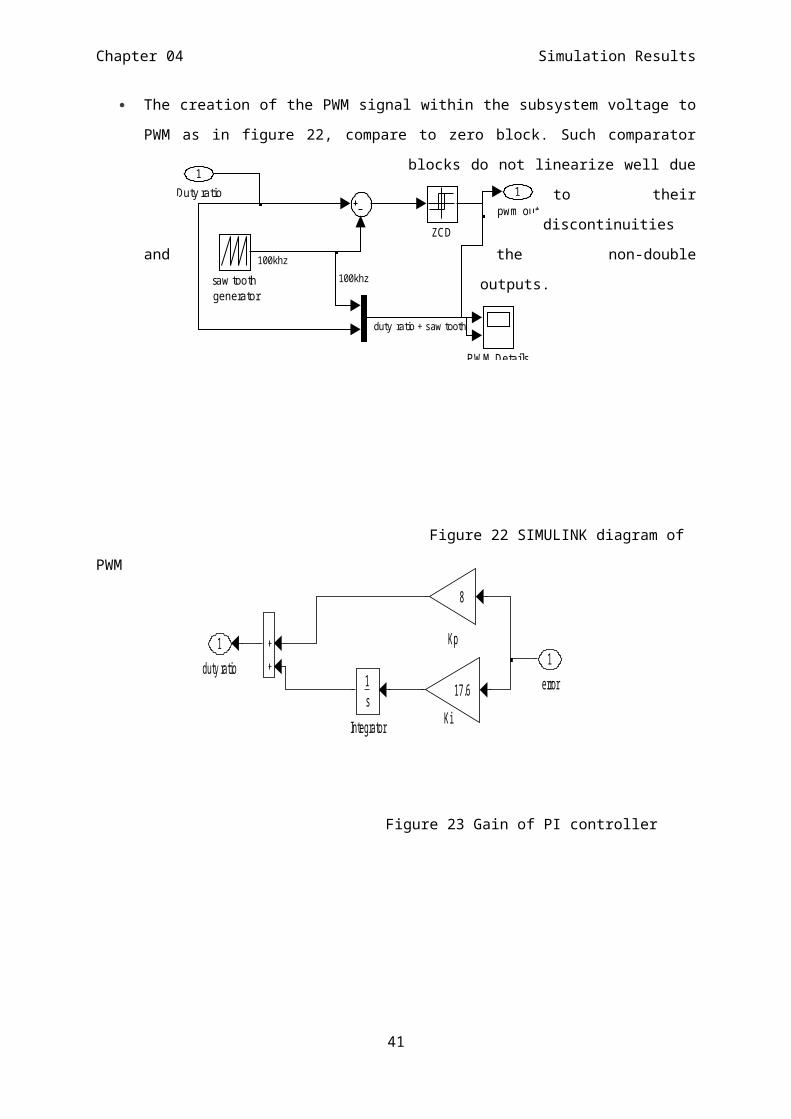
Biblography
Appendix-A
Source Code for PIC16F877A
#include <16F877A.h>
#device adc=10
#fuses hs,nowdt,protect
#use delay(clock=20000000)
#define LCD_RS_PIN PIN_D2
#define LCD_RW_PIN PIN_D3
#define LCD_ENABLE_PIN PIN_C4
#define LCD_DATA4 PIN_D5
#define LCD_DATA5 PIN_C6
#define LCD_DATA6 PIN_C7
#define LCD_DATA7 PIN_D4
#include "lcd.c"
/////////////////////////////////variable
float buck_feedback;
int duty1=50;
////////////////////////////////////////////////////////////
int32 process_analog(char i);
void process_buck();
void process_rpm();
int16 rpm_counter=0,rpm=0,time_counter=0;
int1 time_flag;
45
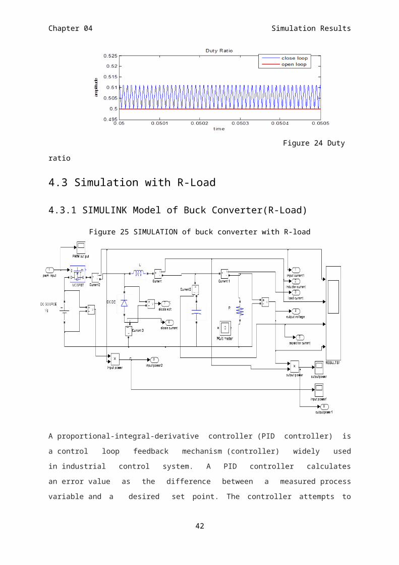
Biblography
//////////////////////////////////////////////////
#int_ext
void external_isr()
rpm_counter++;
////////////////////////////////////////////////////
#INT_TIMER1
void timer1_isr()
time_counter++;
if(time_counter>8)
time_flag=1;rpm=rpm_counter;rpm_counter=0;time_counter=0;output_high(pin_b6);
output_toggle(pin_b7);
///////////////////////////////////////////////////////////
void main()
delay_ms(500);
SETUP_TIMER_1(T1_INTERNAL|T1_DIV_BY_8);
enable_interrupts(int_timer1);
enable_interrupts(int_ext);
ext_int_edge( H_TO_L );
enable_interrupts(global);
setup_adc_ports( ALL_ANALOG );
setup_adc(ADC_CLOCK_INTERNAL );
46

Biblography
setup_timer_2(T2_DIV_BY_4, 124, 1);
setup_ccp1(CCP_PWM);
set_pwm1_duty(duty1);
lcd_init();
LCD_PUTC("WORKING");
while(true)
process_buck();
if(time_flag)output_low(pin_b6);time_flag=0;process_rpm();
delay_ms(100);
///////////////
void process_rpm()
lcd_gotoxy(1,2);
rpm=rpm*60;
printf(lcd_putc,"RPM=%Lu ",rpm);
///////////////////////////////////////////////////////////
void process_buck()
buck_feedback=process_analog(0);
buck_feedback=buck_feedback/10;
if(buck_feedback>12.1) duty1-=1; if(duty1<10) duty1=10;
else if(buck_Feedback<11.9) duty1+=1;if(duty1>120) duty1=120;
47
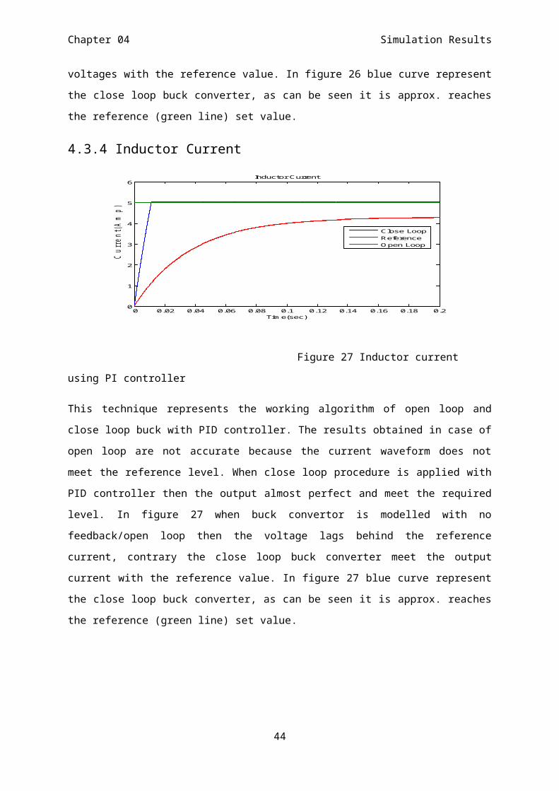
Biblography
set_pwm1_duty(duty1);
lcd_gotoxy(1,1);
printf(lcd_putc,"DU1=%03u",duty1);
printf(lcd_putc," BKV=%3.1f",buck_Feedback);
delay_ms(10);
/////////////////////////
int32 process_analog(char i)
int32 analog_Value;
set_adc_channel(i);
delay_us(10);
analog_value=read_adc();
analog_value=(analog_Value*500)/1023;
return analog_value;
//////////////////////////////////////////////////////////
48
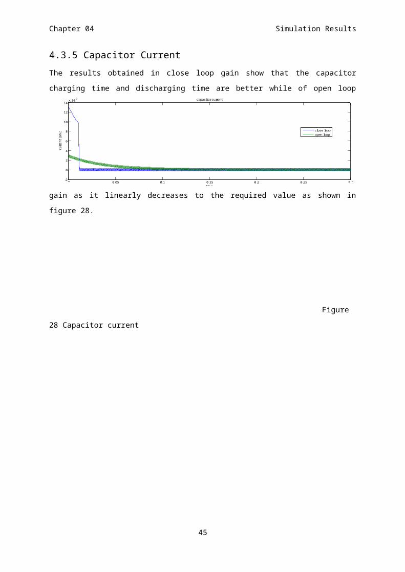
Biblography
49

Biblography
Appendix-B
PIC Microcontroller overviewThe microcontroller PIC16F877A offer cost efficient solution for general purpose applications written
in C. PIC16F877A devices provide flash program memory in sizes from 8 to 128Kbytes and data
memory from 256 to 4Kbytes, operating at a range of 2.0 to 5.0 volts, at speeds from DC to 40MHz.
Basic Features
77 instructions
PIC16 source code compatible
Program memory addressing up to 2Mbytes
Data memory addressing up to 4Kbytes
DC to 40MHz operation
Interrupt priority levels
16-bit-wide instructions, 8-bit-wide data path
Two 8-bit timers/counters
Three 16-bit timers/counters
Four external interrupts
High current (25mA) sink/source capability
Up to five capture/compare/PWM modules
Two USART modules
Parallel slave port (PSP)
Fast 10-bit analog-to-digital converter
Programmable low-voltage detection (LVD) module
Power-on reset (POR), power-up timer (PWRT), and oscillator start-up timer (OST)
In-circuit programming
Table 1 Specifications of PIC16F877A Microcontroller
Feature Specifications
Program memory (Bytes) 32K
Data memory (Bytes) 1536
EEPROM (Bytes) 256
I/O Ports A,B,C,D,E
Timers 4
Interrupt sources 18
50
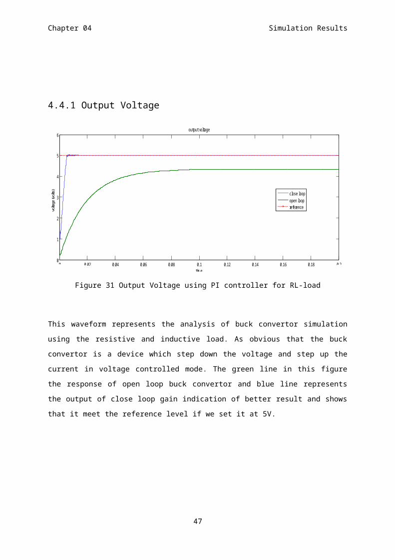
Biblography
Capture/compare/PWM 2
Serial communication MSSP
USART
A/D converter (10-bit) 8 channels
Low-voltage detect Yes
Brown-out reset Yes
Packages
40-pin DIP
44-pin PLCC
44-pin TQFP
IRF-540Features• 28A, 100V
• rDS(ON) = 0.077Ω
• Single Pulse Avalanche Energy Rated
• Nanosecond Switching Speeds
• Linear Transfer Characteristics
• High Input Impedance
51