Embed Size (px)
Citation preview

SS LSemiconductor System Lab
Sungdae Choi 1
Design and Implementation of High Performance
Application Specific Memory
M.S. Thesis
Sungdae ChoiDec. 20th, 2002
- 고성능 Application Specific Memory의 설계와 구현 -

Sungdae Choi 2SS LSemiconductor System Lab
Outline
• Introduction• Memory for Mobile 3D Graphics• Content-Addressable-Memory (CAM) for
Network Memory• Conclusion

Sungdae Choi 3SS LSemiconductor System Lab
Outline
• Introduction– Motivation– Related Work– This Work
• Memory for Mobile 3D Graphics• Content-Addressable-Memory (CAM) for
Network Memory• Conclusion

Sungdae Choi 4SS LSemiconductor System Lab
Motivation(1/2)• Conventional Memory Architecture
– Designed for General Applications• Not Optimized for Specific Application
– Long tRC (60~80ns)• For Mass Production & Low Cost• Bottleneck of the System Performance
– Only Read / Write operation
Need for Application Specific Memory

Sungdae Choi 5SS LSemiconductor System Lab
Motivation(2/2)
• Application Specific Memory– “Offer Unique Characteristics to Improve
Performance in Particular Application”*– Free Design
• Flexible Control• Guaranteed Bandwidth• Low Power Consumption
– Complex Design• Both Memory and System Background
* IEEE Circuits & Devices, “High-Speed Memory Architectures for Multimedia Applications”, 1997

Sungdae Choi 6SS LSemiconductor System Lab
• Cache DRAM (CDRAM)*– DRAM Density + SRAM Speed
• Video RAM (VRAM)*– Requirement for High-quality Display
• Media-Chip**– Embedded Memory for PC 3D Graphics
• Content-Addressable-Memory (CAM)***– High-speed Search Function
Application Specific Memory
* IEEE Circuits & Devices, “High-Speed Memory Architectures for Multimedia Applications”, 1997** Takao Watanabe, “A Modular Architecture for a 6.4Gbyte/s 8Mb DRAM-Integrated Media Chip”, 1997
*** IEEE Potentials, “RAM versus CAM”, 1997

Sungdae Choi 7SS LSemiconductor System Lab
• Memories for Mobile 3D Graphics– Embedded in RamP-IV Processor– Implemented using 0.16um DRAM Process
• Content-Addressable-Memory (CAM) for Network Lookup Engine– Ternary Cell Structure– Simulation using 0.35um Logic Process
Thesis Work
Memory Architecture Contributes the System Performance

Sungdae Choi 8SS LSemiconductor System Lab
Outline
• Introduction• Memories for Mobile 3D Graphics
– Need for Special Memory– Memory Specification– Applied Architectures– Simulation Results– Chip Implementation
• Content-Addressable-Memory (CAM) for Network Memory
• Conclusion

Sungdae Choi 9SS LSemiconductor System Lab
RamP-IV Processor*
• For Mobile Multimedia Application
* R. Woo, et. al., "A 210mW Graphics LSI Implementing Full 3D Pipeline with 264Mtexels/s Texturing for Mobile Multimedia Applications“, ISSCC 2003

Sungdae Choi 10SS LSemiconductor System Lab
3D Graphics in RamP-IV• Target Performance for High-Quality 3D Graphics
– Mobile Application• 256 x 256 resolution @ 24bit color• 16bit depth-comparison
– High Image Quality• Double Frame Buffering• Texture Mapping
– High Performance• Double Pixel Processor• 100Mpixel/sec Performance
Polygon Setup
Z Compare
Rendering
Color Porcessing
Alpha Blending
TextureProcessing
Memories in the Rendering Engine
Need for New Memories to Supply the Performance
TM
ZB
FB

Sungdae Choi 11SS LSemiconductor System Lab
Memories for Target Performance
• Frame-Buffer– 24bit I/O bus (for 24bit color processing)– 3Mb capacity (256 x 256 x 24bit x double FB)
• Individual 768kb x 4 (for double pixel processing)– Read-Modify-Write Operation
• Simplifies the Pile-line Stage of the Rendering Engine– 20ns tRC (for 100Mpixel/s performance)
• Conventional Memory has 60~80ns tRC Frame Buffer
Frame Buffer
Frame Buffer
Frame Buffer
Depth Buffer
Depth Buffer
Depth Buffer
Depth Buffer
Text
ure
Mem
ory
Text
ure
Mem
ory
Text
ure
Mem
ory
Text
ure
Mem
ory
RamPRendering Engine 3Mb2Mb
24Mb
Sungdae Choi 12SS LSemiconductor System Lab
Memories for Target Performance
• Z-Buffer– 16bit I/O bus (for 16bit depth comparison)– 2Mb capacity (256 x 256 x 16bit depth x double FB)
• Individual 512kb x 4 (for double pixel processing)– Read-Modify-Write Operation
• Simplifies the Pipe-line Stage of the Rendering Engine– 20ns tRC (for 100Mpisel/s performance)
Frame Buffer
Frame Buffer
Frame Buffer
Frame Buffer
Depth Buffer
Depth Buffer
Depth Buffer
Depth Buffer
Text
ure
Mem
ory
Text
ure
Mem
ory
Text
ure
Mem
ory
Text
ure
Mem
ory
RamPRendering Engine 3Mb2Mb
24Mb

Sungdae Choi 13SS LSemiconductor System Lab
Memories for Target Performance
• Texture Memory– 24bit I/O bus (for 24bit color processing)– 20ns tRC (for 200Mtexel/s performance)– Read Oriented Operation– 24Mb capacity = 6Mb x 4 (for bilinear interpolation)
Frame Buffer
Frame Buffer
Frame Buffer
Frame Buffer
Depth Buffer
Depth Buffer
Depth Buffer
Depth Buffer
Text
ure
Mem
ory
Text
ure
Mem
ory
Text
ure
Mem
ory
Text
ure
Mem
ory
RamPRendering Engine 3Mb2Mb
24Mb

Sungdae Choi 14SS LSemiconductor System Lab
Memory Specification
24bit R/W Bus16bit Write Bus16bit Read Bus
24bit Write Bus24bit Read Bus
Data pin
24bit15bitAddress Pin
CLKREADWRITEREF
CLK - Clock InputRMW - RMW CommandMASK – Write Mask SignalREF – Auto Refresh Command
Control Pin
ReadWriteAuto RefreshNOP
Read-Modify-Write (RMW)Auto RefreshNOP
Function
6Mb512kb768kbMemory Size20nstRC
Texture MemoryZ-BufferFrame-Buffer

Sungdae Choi 15SS LSemiconductor System Lab
Design Restriction
• “Always Complete RMW within 20ns” for Constant Performance of the Rendering Engine– tRC = 20ns
• “Precharge - Activation - CMD” within 20ns– Burst Access function is useless.
• Page Access Mode enhances burst access latency.• Partial Activation reduces power consumption.
– Conventional SDRAM interface scheme requires high clock frequency for 20ns tRC
CLOCK
ADDR Ra Ca0
DQ CL=2
Row Acive Read Precharge
R1 M1 W1
0 1 2 3 4 5 6 7 8 9 10
7 cycle for RMW = 350MHz Clock

Sungdae Choi 16SS LSemiconductor System Lab
Architecture(1/5)• Single Clock Operation
– Finish “Precharge-Activation-CMD” in one cycle– SRAM-like Easy Control– Simplifies the pipeline control of the rendering engine– Low-Power Consumption due to Low Clock Frequency
FB&ZB RMW Timing Diagram
W1
C1
0 10ns 20ns
Clock
CMD & ADR
40ns
Read Out
15ns
Write In
MASK
C2
W2
R2R1
Modify WritePCG Active & Read
1ns
Operation Modify CanceledWritePCG Active & Read

Sungdae Choi 17SS LSemiconductor System Lab
Architecture(2/5)
• Partial Activation– Consumes lower power than Page-Access-Mode
I/Octl
SA
cellarrayblock S
WD
SW
D
SW
DSW
D cellarrayblock
DBSA &
Write Driver
sws3
sws0 sws1
sws[3:0]
PXA[n]
SA_ctl_T
SA_ctl_0
SA_ctl_1
I/O ctl signal
Row Address decoded signal
Row Address decoded signal
Col. gate control_T
Col. gate control_0
Col. gate control_1
DQR[23:0] DQW[23:0]
sws2
SA
SA
PXA

Sungdae Choi 18SS LSemiconductor System Lab
Architecture(3/5)
• Speed-Optimized Cell Architecture– Minimize Wire-Delay
(a) Cell Array of the Frame-Buffer (b) Cell Array of the Z-Buffer
SWD SWD
SASA
256cell/BL
192cell/SWL
SWD SWD
SASA
SASA
SWD SWD
SASA
256cell/BL
128cell/SWL
SWD SWD
SASA
SASA
(c) Cell Array of the Texture Memory
SASA
512cell/BL
384cell/SWL
SASA
SASA

Sungdae Choi 19SS LSemiconductor System Lab
Architecture(4/5)• Non-Multiplexed Addressing Scheme
– Decodes both row and column address at a time– Reduces address decoding time
PCG
DBSA
Fetc
h
Write
ATV
Modify
Frame-Buffer & Z-Buffer
Clock
AddressDec.

Sungdae Choi 20SS LSemiconductor System Lab
Architecture(5/5)
• Variable Clock Operation– Support Long-Lasting Operation in the System Level
0ns 20ns 40ns 60ns 80ns 100ns
NORMAL Mode
SLOW Mode
Operation Operation Operation Operation Operation
Operation Operation Operation
Operation Operation
FAST Mode
ATV W
ATV W
ATV W
W
Write Latch
Write Latch
ATV W
ATV
ATV
Write Latch
ATV W
W
ATV W
W
ATV W
W
ATV W
WRendering Engine
Memory Timing
15ns
Sungdae Choi 21SS LSemiconductor System Lab
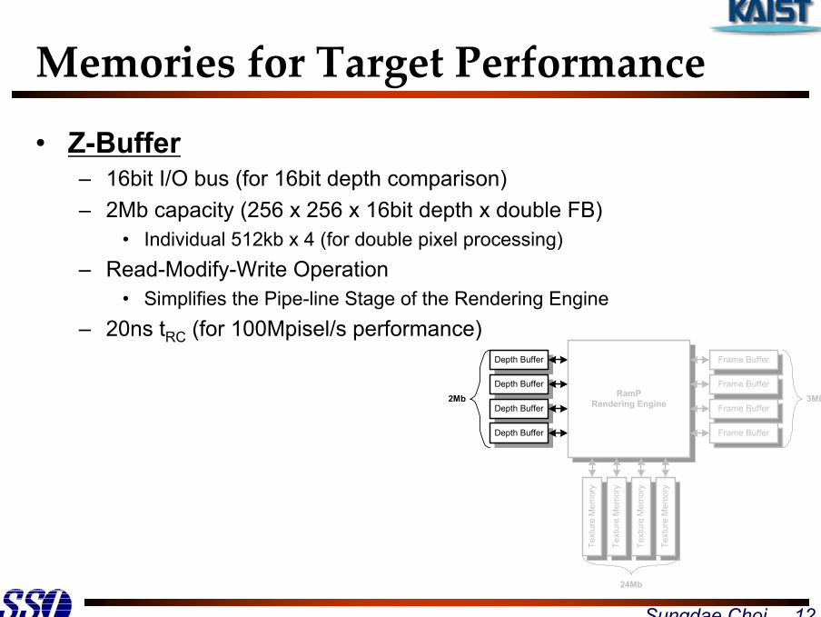
Implementation(1/2)
• Overall Structure
Unit Block Driver
SACtl&
WLD
CMDBlock
CtlPulseGen.
WriteIn
Driver
ReadOut
Driver
/
/
UnitBlock
UnitBlock
UnitBlock
UnitBlock
UnitBlock
UnitBlock
UnitBlock
UnitBlock
CMD
Clock
WriteInput
ReadOutput
24b or 16b/
24b or 16b/

Sungdae Choi 22SS LSemiconductor System Lab
Implementation(2/2)
• Unit Block Control
BLSA
DBSA
SACtl
WDRV
ControlPulse
Generator
ADDR
CMD
RowDecoder
ColumnDecoder
BlockSelector
I/OSubCtl
I/OCtl
CLK
WL_ATV
SAEN...
CDen
IO_CTL...
Block_ctl
Block_ctl
BlockPower
CLK
PCG
WL_ATV
SA_EN
READ
WRITE
Sungdae Choi 23SS LSemiconductor System Lab
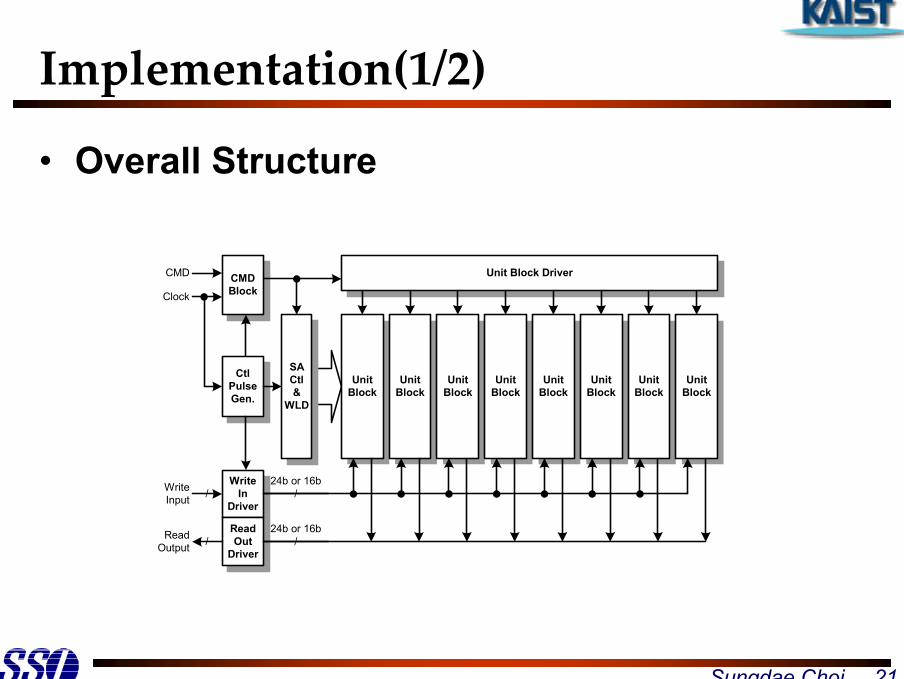
Simulation Results(1/2)
• Read-Modify-Write Waveform
Precharge Activation Read Modify Write

Sungdae Choi 24SS LSemiconductor System Lab
Simulation Results(2/2)
• Operation Waveform
RMW RMW NOP NOP RMW REFRMW REF RMW RMWRMWMASK
RMWMASK
RMWMASK
RMWMASK
RMWMASK

Sungdae Choi 25SS LSemiconductor System Lab
Chip Micrograph(1/3)
• Frame-Buffer
2mm
0.56
mm
* 0.16um DRAM technology

Sungdae Choi 26SS LSemiconductor System Lab
Chip Micrograph(2/3)
• Z-Buffer
1.6mm
0.56
mm

Sungdae Choi 27SS LSemiconductor System Lab
Chip Micrograph(3/3)
• Texture Memory
3mm
1.2m
m

Sungdae Choi 28SS LSemiconductor System Lab
Measurement
Using Probe-Station

Sungdae Choi 29SS LSemiconductor System Lab
Performance Comparison
Embedded DRAMPC 3D GraphicsMobile 3D GraphicsTarget
3.8Gb/s12.8Gb/s Max.1.2Gb/s2.4Gb/s (RMW)Bandwidth
2.4mm2/Mb(2.9mmx2.0mm)
155mW Max.110mW Typ.
SRAM-like
1
160MHz
2.4M
0.25um DRAM
Memory2**
SDRAM-likeSRAM-likeSRAM-likeInterface
RMWMASKReadWrite
6.4mm2/Mb(2.95mmx4.37mm)
0.6mm2/Mb(3.0mmx1.2mm)
< 1.5mm2/Mb(2.0mmx0.56mm)
Chip Size
160mW18mW27mW
20mW9mW
Power
2:Read 1:Write+ Activation Period
11Latency
100MHz50MHz50MHzClock
2Mb6Mb768kbMemory Size
0.40um DRAM0.16um DRAM0.16um DRAMProcess
Memory1*Texture MemoryFrame-Buffer
* Takao Watanabe, “A Modular Architecture for a 6.4-Gbyte/s, 8-Mb DRAM-Integrated Media Chip”, 1997** Paul DeMone, “A 6.25ns Random Access 0.25um Embedded DRAM”, 2001
Low-Power & Optimized Operation for Mobile 3D Graphics

Sungdae Choi 30SS LSemiconductor System Lab
Outline
• Introduction• Memories for Mobile 3D Graphics• Content-Addressable-Memory (CAM) for
Network Memory– Lookup Engine in a Network Processor– Problem of Conventional CAM– Proposed CAM for Lookup Engine– Simulation Results
• Conclusion

Sungdae Choi 31SS LSemiconductor System Lab
Lookup Engine in a Network Processor
• Lookup Engine– Searches Tag for incoming Packet– Has Lookup Memory (Rule Memory)– “Search” is main job
PacketProcessor
Packet 1
Packet 2
Packet 3
Packet 1
Packet 2
Packet 3
Tag B
Tag C
Tag A
LookupEngine

Sungdae Choi 32SS LSemiconductor System Lab
Implementing Lookup Engine
• Conventional Memory Architecture*– Requires Frequent Memory Access– Consumes Many Clock Cycle Low Performance
• CAM Architecture– Enables One-Cycle Search Operation– Large Power & Area Consumption
CAM is preferred.
* Miguel A. Ruiz-Sanchez, “Survey and Taxonomy of IP Address Lookup Algorithms”, 2001

Sungdae Choi 33SS LSemiconductor System Lab
Conventional NAND type
ML
BL BL#
WL
Conventional CAM
• Structure of Conventional CAM*
☺ Low Power ConsumptionSlow Match Line PropagationCannot handle ‘Don’t Care’
☺ Fast Match Line PropagationLarge Power ConsumptionCannot handle ‘Don’t Care’
Conventional NOR type
BL BL#
WL
ML
* Ilion Yi-Liang Hsiao, et. al., “Power Modeling and Low-Power Design of Content Addressable Memories”, ISCAS 2001

Sungdae Choi 34SS LSemiconductor System Lab
Conventional TCAM(1/3)
• Need for ‘Don’t Care’
‘Don’t Care’ reduces the size of routing table.
L1203.*.*.*
L6203.238.128.*
L5203.238.128.56
L2143.248.*.*
L9*
Next hopPrefix
L6203.238.128.255
L6…
L6203.238.128.2
L6203.238.128.1
L5203.238.128.56
L2143.248.255.255
L2…
L2143.248.1.2
L2143.248.1.1
Next hopPrefix
Routing Table without Don’t Care
Routing Table using Don’t Care

Sungdae Choi 35SS LSemiconductor System Lab
Conventional TCAM(2/3)
B1 B1#
WL
ML
B2 B2#
q1 q1' q2 q2'
00*011100
q2q1
• Handling Don’t Care
Encode Don’t Care using Two CAM Cells*
* Sergio R. Ramirez-Chavez, “Encoding Don’t Cares in Static and Dynamic CAMs”, 1992
2 BCAMs build 1 TCAM

Sungdae Choi 36SS LSemiconductor System Lab
Conventional TCAM(3/3)• Dynamic TCAM*
– Use Gate Cap. as a storage• DRAM CAM**
– 2 DRAM cells for one TCAM• Multiple-Valued CAM***
– EEPROM technology
* JON P. WADE, “A Ternary Content Addressable Search Engine”, 1989
** Tadato Yamagata, “A 288kb Fully Parallel Content Addressable Memory Using a Stacked-Capacitor Cell Structure”, 1992
*** Takahiro Hanyu, “Design of a One-Transistor-Cell Multiple-Valued CAM”, 1996
BottleneckRefresh Operation
Core speedTechnology
…

Sungdae Choi 37SS LSemiconductor System Lab
Proposed CAM(1/3)
• Ternary CAM Cell Structure
Proposed NAND type
ML
BL BL#
WL
DCL DCL# BL BL#
WL
DCL DCL#
ML
Proposed NOR type
Store1 or 0
StoreBin or X
NAND type consumes less power.
Patent Pending 2002/11Patent Pending 2002/11
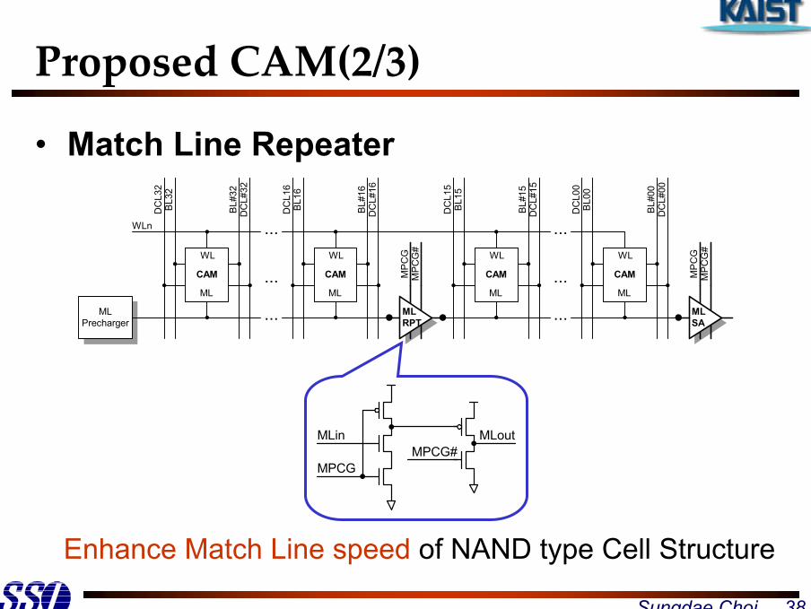
Sungdae Choi 38SS LSemiconductor System Lab
Proposed CAM(2/3)
• Match Line Repeater
Enhance Match Line speed of NAND type Cell Structure
CAM
WL
ML
CAM
WL
ML...
...
...
CAM
WL
ML
CAM
WL
ML...
...
...D
CL#
32B
L#32
DC
L32
BL3
2
DC
L#16
BL#
16
DC
L16
BL1
6
DC
L#15
BL#
15
DC
L15
BL1
5
DC
L#00
BL#
00
DC
L00
BL0
0
MLSA
WLn
MLPrecharger
MLRPT
MP
CG
#M
PC
G
MP
CG
#M
PC
G
MPCGMPCG#
MLin MLout

Sungdae Choi 39SS LSemiconductor System Lab
Proposed CAM(3/3)
• 2-D Decoding Method– By Long Aspect Ratio of the Proposed Cell
ML0ML1ML2ML3
WL
MLout
SWD
MLS
A
32bit TCAM Unit

Sungdae Choi 40SS LSemiconductor System Lab
Simulation Results
• Match Line Propagation
More than x3 Faster than Conventional Scheme
Proposed SchemeConventional SchemeFinal Match Out
Unmatch Match
5ns

Sungdae Choi 41SS LSemiconductor System Lab
Cell Size
DCL BL BL# DCL#
ML ML
WL WL
ML ML
WL WL
BL BL#
Proposed Cell Conventional Cell
25% smaller than conventional TCAM
DCL DCL#

Sungdae Choi 42SS LSemiconductor System Lab
Expected Performance
70MHz30MHz100MHzClock
NORNANDNANDMatch Line Type
pMOS NOR typeSeparated Bit-Line and Search-LineStore Don’t CareEtc
7.3ns for Search Evaluation
26ns for Search Out
5nsfor Search Evaluation
Search Speed
131fJ/Bit/Search83fJ/Bit/Search100~120fJ/Bit/SearchSearch Power Dissipation
256 x 54bitBinary
64k x 40bitBinary
64k x 32bitTernary
Memory Capacity
0.35um Standard0.35um 5M1P0.35um CMOSProcess
JSSC 2001**JSSC 1998*Proposed
* Farhad Shafai, et al, “Fully Parallel 30-MHz, 2.5-Mb CAM”, JSSC November 1998** Hisatada Miyatake, et al, “A Design for High-Speed Low-Power CMOS Fully Parallel
Content-Addressable Memory Macros”, JSSC June 2001

Sungdae Choi 43SS LSemiconductor System Lab
Outline
• Introduction• Memories for Mobile 3D Graphics• Content-Addressable-Memory (CAM) for
Network Memory• Conclusion

Sungdae Choi 44SS LSemiconductor System Lab
Conclusion
• Application Specific Memory Architectures are Proposed.– Frame-Buffer, Z-Buffer and Texture Memory for Mobile 3D
Rendering Engine– Ternary-CAM Structure for Network Lookup Engine
• Mobile 3D Graphic Memories are Implemented.– 0.16um DRAM Technology.– 20ns tRC with Read-Modify-Write Operation.– Improve the performance of the 3D Graphics System.
• New Ternary-CAM Structure is Proposed.– 5ns Match Evaluation Time– 25% Reduced Cell Size