Embed Size (px)
Citation preview
[Mishra* et al., 5(8): August, 2016] ISSN: 2277-9655
IC™ Value: 3.00 Impact Factor: 4.116
http: // www.ijesrt.com © International Journal of Engineering Sciences & Research Technology
[325]
IJESRT INTERNATIONAL JOURNAL OF ENGINEERING SCIENCES & RESEARCH
TECHNOLOGY
DESIGN AND IMPLEMENTATION OF HIGH SPEED AES ALGORITHM FOR DATA
SECURITY Archana Mishra*, Sourabh Sharma
* M-Tech VLSI Scholar Trinity Institute of Technology and Research, Bhopal Mp India
Asst. Professor EC Dept.
DOI: 10.5281/zenodo.59643
ABSTRACT In the current cyber era, 44% of the Indians use internet today and the numbers are increasing exponentially in recent
years. It is accepted truth that in the coming year’s security architecture in cyberspace decides growth of nation.
In this paper, we present a VLSI based AES (Advanced Encryption Standard) encryption that effectively addresses
espionage and fraudulent cybercrime based cyber attacks. It is most commonly used symmetric block cipher
algorithm that transform information into obscure data based on key-defined transformation set. In addition, it is
lossless operation with size of input and output being the same and could be extended to a wide range of applications.
We limit our focus to128-bit AES encoding and decoding operations over VHDL coded transformation that requires
key for successful completion of the operation With rise in several methods proposed for implementation of data
security it has become more vital for a feasibility study of any hardware design is essential i.e. to test encryption and
decryption process of the proposed 128-bit AES algorithm. In the simulations results, we analyze the each of the
transformation that is incorporated for coding on FPGA using Xilinx ISE tool.
KEYWORDS: Encryption, FPGA, Advance Encryption Standard, Xilinx, Data Security.
INTRODUCTION“Digital India” program significant portion of government records, personnel information, and financial details of
Indians would available online [1]. Its main aim was to enhance the electronic literacy among the people so that they
could acknowledge the concern government benefits which in turn reduce corruption. Unfortunately, every person’s
financial, medical, social and criminal history would be online and digitally available for individuals of both nature
(i.e. good and bad). Henceforth, the demand for the data security has been growing exponentially now-a-days.
Fundamentally data security deals with the two practices for developing algorithms namely:
1. For preserving the integrity of data in consideration
2. For preserving the information of data in consideration
Even though both the practices sound similar there is significant difference between both i.e. one preserves the
integrity of the information by detecting any changes in data (for example: hashing algorithms). Most of the world is
dependent upon software that protects the information of data (for example: encryption). This fact signifies the
predominance of security activities in the current digital and cyber era. In general these algorithms will be developed
with series of different activities which need to be carried out simultaneously [2]. With the recent developments in the
digital technology have increased the ease with which multimedia data are reproduced and retransmitted. These
developments have increased the potential of data manipulation and alteration of digital data with little distortion.
Typically, a covert communication system can be viewed as secured communication system wherein the data that is
being communicated in unintelligible nature. Cryptography is one of the approaches that provide the solution for a
covert communication system based on mathematical and/or statistical transformation. Existing algorithms for
cryptography can be broadly classified into two classes depending on cipher code generated:
1) Stream cipher and
[Mishra* et al., 5(8): August, 2016] ISSN: 2277-9655
IC™ Value: 3.00 Impact Factor: 4.116
http: // www.ijesrt.com © International Journal of Engineering Sciences & Research Technology
[326]
2) Block cipher
Most of the researchers have focused on transformation in the block cipher domain as it attains a higher robustness.
Block cipher based cryptography is one of the active research area, that develop methods to protect against privacy of
multimedia and visual surveillance system for security proposes. Henceforth, we a brief review on each of systems in
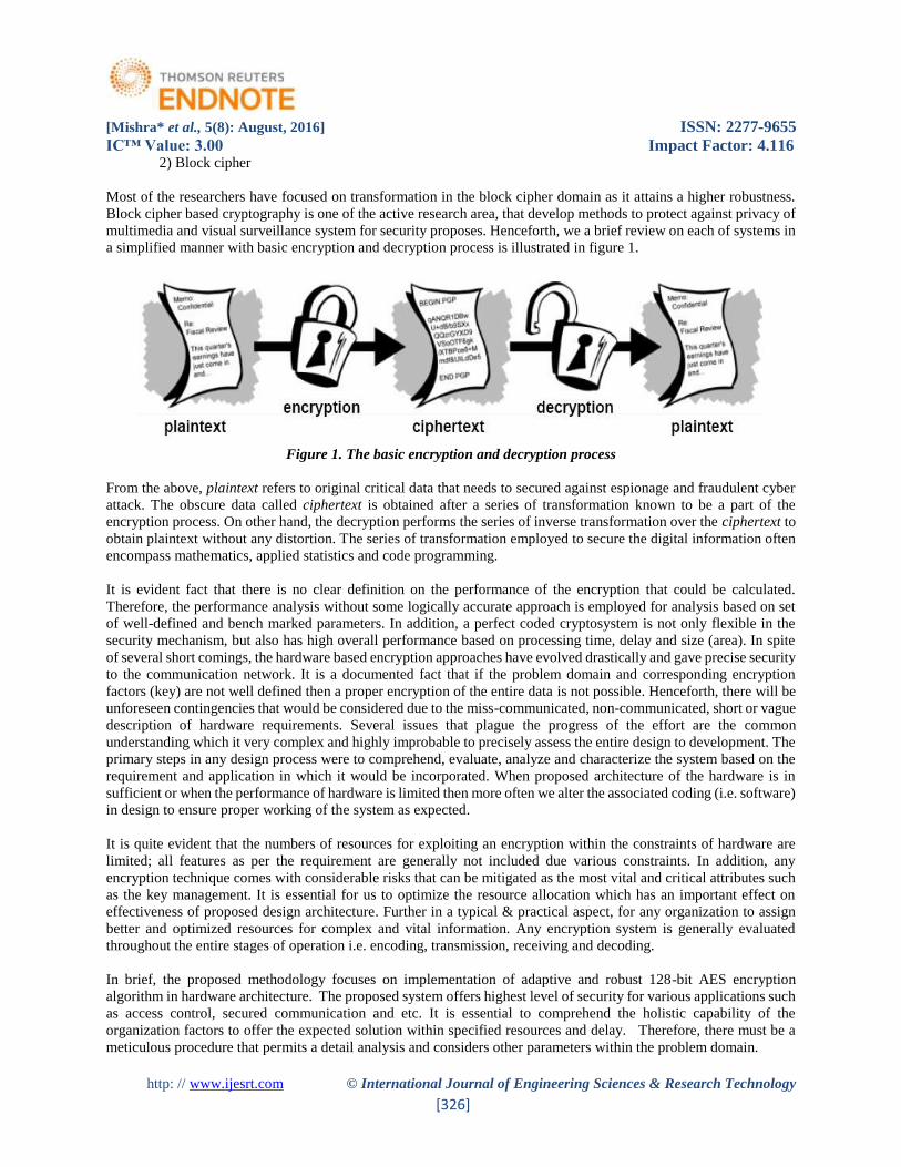
a simplified manner with basic encryption and decryption process is illustrated in figure 1.
Figure 1. The basic encryption and decryption process
From the above, plaintext refers to original critical data that needs to secured against espionage and fraudulent cyber
attack. The obscure data called ciphertext is obtained after a series of transformation known to be a part of the
encryption process. On other hand, the decryption performs the series of inverse transformation over the ciphertext to
obtain plaintext without any distortion. The series of transformation employed to secure the digital information often
encompass mathematics, applied statistics and code programming.
It is evident fact that there is no clear definition on the performance of the encryption that could be calculated.
Therefore, the performance analysis without some logically accurate approach is employed for analysis based on set
of well-defined and bench marked parameters. In addition, a perfect coded cryptosystem is not only flexible in the
security mechanism, but also has high overall performance based on processing time, delay and size (area). In spite
of several short comings, the hardware based encryption approaches have evolved drastically and gave precise security
to the communication network. It is a documented fact that if the problem domain and corresponding encryption
factors (key) are not well defined then a proper encryption of the entire data is not possible. Henceforth, there will be
unforeseen contingencies that would be considered due to the miss-communicated, non-communicated, short or vague
description of hardware requirements. Several issues that plague the progress of the effort are the common
understanding which it very complex and highly improbable to precisely assess the entire design to development. The
primary steps in any design process were to comprehend, evaluate, analyze and characterize the system based on the
requirement and application in which it would be incorporated. When proposed architecture of the hardware is in
sufficient or when the performance of hardware is limited then more often we alter the associated coding (i.e. software)
in design to ensure proper working of the system as expected.
It is quite evident that the numbers of resources for exploiting an encryption within the constraints of hardware are
limited; all features as per the requirement are generally not included due various constraints. In addition, any
encryption technique comes with considerable risks that can be mitigated as the most vital and critical attributes such
as the key management. It is essential for us to optimize the resource allocation which has an important effect on
effectiveness of proposed design architecture. Further in a typical & practical aspect, for any organization to assign
better and optimized resources for complex and vital information. Any encryption system is generally evaluated
throughout the entire stages of operation i.e. encoding, transmission, receiving and decoding.
In brief, the proposed methodology focuses on implementation of adaptive and robust 128-bit AES encryption
algorithm in hardware architecture. The proposed system offers highest level of security for various applications such
as access control, secured communication and etc. It is essential to comprehend the holistic capability of the
organization factors to offer the expected solution within specified resources and delay. Therefore, there must be a
meticulous procedure that permits a detail analysis and considers other parameters within the problem domain.
[Mishra* et al., 5(8): August, 2016] ISSN: 2277-9655
IC™ Value: 3.00 Impact Factor: 4.116
http: // www.ijesrt.com © International Journal of Engineering Sciences & Research Technology
[327]
BACKGROUND In this section, we consolidate the brief background on various attributes and functionalities that are factored in
designing the architectures of existing AES encryption technique while addressing hardware issues such as area, power
and throughput. Although some these are very popular than others techniques that address data security issues, the
constraints associated with performance, size and power that differentiate each of these architectures. It is evident that
each technique has several advantages and corresponding limitations, so to obtain an precise analysis all techniques
needs to be employed that will make the entire process complex and very costly. The excellence and scope of
cryptography based approaches doesn’t limit to the securing the digital assets in consideration, but based on the time
taken for the breaking the obscure information into meaning data by malicious eavesdropper. AES (Advanced
Encryption Standard) is the popular eminent algorithmic frameworks that are commonly employed for effective
encryption whose key parameters can be designed that are adaptive to application based development platform, which
is vital aspect for encryption algorithm [4].
Advanced Encryption Standard (AES) (commonly coined as Rijndael) is a symmetric block cipher standardized by
NIST for securing information. In this thesis, we limit to design and implementation of 128-bit AES encoding and
decoding techniques wherein VHDL coding is employed for defining the transformations during encoding phase and
inverse transformation during the decoding phase of the system. The synthesized analysis was simulated Virtex-2
based FPGA while feasibility of the approach is studied using the Xilinx. The transformations are defined as the set
of executable code which performs a computational complex operations in an optimum manner as per the application
requirement. It is vital that the outcome of the system needs to be consistent, efficient and reliable based on the key
applied within the application in consideration [14]. The requirement of the data security is evolving into an active
research area due to the rapid changes in processor speed and application requirements in consideration that operates
the entire system.
Gnanambika, M., Adilakshmi, S., and Noorbasha, D. F [5] proposed hardware implementation of AES that offers high
speed and efficiently addresses the Sub Byte transformation method. This exploits the benefits of combinational logic
performed in polynomial bases while the architecture was implemented by combining composite field arithmetic in
normal bases. Furthermore, key expansion was also presented with a detail and efficient architecture simulated using
Modelsim proves the efficient performance of the system. Kalaiselvi, K., and Mangalam, H. [6] proposed AES
technique with a key expansion process to address low power and high throughput requirements of hardware design.
The overall power consumption of the encryption system is reduced while the delay along the critical path is also
reduced due to optimized architecture. Simulation analysis proves that this architecture offered superior performance
in comparison with other existing architectures in terms of power, throughput and delay. In addition, 256-bit key is
employed during encoding and decoding process.
Das, S. S., and Resmi, R. [7] introduced Advanced Encryption Standard (AES) based VLSI implementation with an
effective and optimized architecture with a module that exploits the key expansion with ROM. The incorporation of
ROM at the cost of commonly used is quite beneficial. Furthermore in an effort to reduce the area and power of the
system registers a novel framework of merging two steps with exclusion of shift rows was studied. The Virtex5 FPGA
was utilized during simulation analysis to study the feasibility modified AES algorithm. The results prove that they
achieve a higher FPGA efficiency (in terms of Throughput and Area) compared to previous existing AES designs.
Dattathreya, K. A., and Kashwan, K. R. [8] developed AES with a multimode multiplier capable to compute
polynomial fields. The Montgomery Multiplication are complex and operational time is high which makes AES
algorithm slow, and power consumed is high that was effectively addressed using a Wallace Tree multiplier. The
delays along the critical paths of the design are optimized by exploiting buffer insertion concept. In addition, design
analysis and synthesis were simulated using Xilinx while the coding was done on Hardware Description Language
(HDL). The results prove that they achieve desired efficiency in comparison with previous existing AES designs and
model.
Meera, R., and Kalaiselvi, K. [9] proposed a 128-bit AES implementation on FPGA that could address information
security issues that has become a prominent area now-a-days. They illustrate various advantages and limitations
associated with implementation with aspect to hardware and software. The results prove that they 128-bit AES
[Mishra* et al., 5(8): August, 2016] ISSN: 2277-9655
IC™ Value: 3.00 Impact Factor: 4.116
http: // www.ijesrt.com © International Journal of Engineering Sciences & Research Technology
[328]
approach offers a considerable high efficiency and reduces the computational time taken for key generation. In
addition, the system achieves desired speed while the low area and power are maintained.
Vaidehi, M., and Rabi, B. J. [10] proposed a novel implementation of AES with modified architecture that reduces
the complexity of MixColumn transformation along the critical path. In addition, AES architecture is optimized by
innovative re-designing of MixColumn transformation by minimizing the repetitive logical functions. Thus, this
system addressed the delay, power in an effective manner than the traditional methods realized. VHDL is exploited in
design phase of the system but the Common Sub-expression Elimination (CSE) incorporated to significant and
effectively optimizes the MixColumn transformation of algorithm. Further, design improvement stands at 10.93%
(hardware slices), 13.6% (LUTs) and finally 1.19% (delay). The simulation analysis shows some of the promising
results with 4.75% (area), 4.56% (power) in comparison with traditional MixColumn based AES Encryption.
Zhang, Q. et.al [11] proposed a novel implementation of asynchronous AES with modified architecture with a round
key generation reduces the complexity and delay along the critical path. Even though it is most prominent encryption
technique used as security for financial applications, unfortunately it is not immune to side-channel attacks which are
addressed by the Asynchronous AES design. In brief, this system incorporates a combination of round key generation
and mix column calculation to implement novel design. Furthermore, to reduce the area and power of the system Balsa
HDL properties are incorporated on the basis of GTECH-based design flow. Experimental results prove that this
system offers better performance i.e. 67.7% (lower computation time) and 40% (lower power) while the 7.3% (area)
and 15% (delay) are reported.
Kshirsagar, R. V., and Vyawahare, M. V [12] proposed AES architecture by partitioning of buffer into sub-blocks of
pipeline structure with repetitive AES modules. They are utilized intermediate buffers along with the module of byte
substitute operated over shift rows block (Shift Row). This design improves the area with optimized usage of blocks
while the integrity of the AES encryption algorithm is preserved. The feasibility of the proposed system was carried
out on Xilinx's SPARTAN-3 FPGA that shows promising performance in terms of throughput rate and hardware area.
The simulation results prove that this system offers 56% (area) and 4.25% (delay) in comparison with the existing
algorithms.
Due to the constant exploration within the field of Hardware engineering, there are several commonly used approaches
were proposed for various classes of AES encryption algorithms. These methods available are classified into analogy
based various factors. Based on the simulation results, we observe that each of existing approach has advantages as
well as drawback in comparison with other approaches, as their advantages and limitations are often complimentary
to each other [13-15]. To understand the advantages and limitation of any method it is very important to know when
you can use which method to optimize the resources while maintaining the performance. It is an evident fact that
hardware design is complex problem that doesn’t has a precise solution that could be easily deciphered because there
are several parameters used in the computation for a precise solution i.e. AES encryption algorithm. The prior
understanding helps us in optimizing the resource allocation which has an important effect on effective implementation
of the AES architecture. Regular revaluation is a proven manner to ensure the advancement in design and supervise
the system performance.
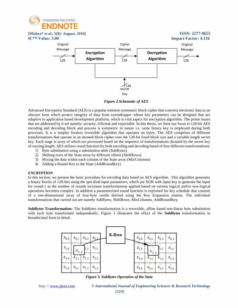
ADVANCED ENCRYPTION STANDARD ALGORITHM Any encryption method consists of two vital sub-blocks that decides its performance and strength i.e., the algorithm
and secret key. As discussed in prior sections, algorithms are usually function based on complex mathematics and/or
statistics with the scope of defined constraints. Whereas the key is a collection of bits, that are essential at various
stages of the algorithm for decoding the information from obscure data. Most of the existing encryption methods can
be classified based on the characteristics of algorithm and key. The entire integrity of the system depends on the
protection of the key as it compromises both the encoding and decoding process as presented in figure 2.
[Mishra* et al., 5(8): August, 2016] ISSN: 2277-9655
IC™ Value: 3.00 Impact Factor: 4.116
http: // www.ijesrt.com © International Journal of Engineering Sciences & Research Technology
[329]
Figure 2.Schematic of AES
Advanced Encryption Standard (AES) is a popular eminent symmetric block cipher that converts electronic data to an
obscure form which protect integrity of data from eavesdropper whose key parameters can be designed that are
adaptive to application based development platform, which is vital aspect for encryption algorithm. The prime issues
that are addressed by it are namely: security, efficient and exportable. In this thesis, we limit our focus to 128-bit AES
encoding and decoding block and process is symmetric in nature i.e. same binary key is employed during both
processes. It is a simpler lossless reversible algorithm that operates on bytes. The AES comprises of different
transformations that operate in an iterated block cipher over the 128-bit fixed block size and a variable length secret
key. Each stage is array of which are processed based on the sequence of transformations dictated by the secret key
of varying length. AES utilizes round function for both encoding and decoding based of four different transformations:
1) Byte substitution using a substitution table (SubBytes)
2) Shifting rows of the State array by different offsets (ShiftRows)
3) Mixing the data within each column of the State array (MixColumns)
4) Adding a Round Key to the State (AddRoundKey)
ENCRYPTION
In this section, we present the basic procedure for encoding data based on AES algorithm. This algorithm generates
a binary blocks of 128-bits using the specified input parameters, which are XOR with input key to generate the input
for round-1 as the number of rounds increases transformations applied based on various logical and/or non-logical
operations becomes complex. In addition a parameterized round function is exploited for key schedule that consists
of a one-dimensional array of four-byte words derived using the Key Expansion routine. The individual
transformations that carried out are namely SubBytes, ShiftRows, MixColumns, AddRoundKey.
SubBytes Transformation: The SubBytes transformation is a reversible, affine based non-linear byte substitution
with each byte transformed independently. Figure 3 illustrates the effect of the SubBytes transformation in
hexadecimal form in detail.
Figure 3. SubBytes Operation of the State
Encryption
Algorithm
Decryption
Algorithm
Original
Message
Cipher
Message
Original
Message
Secret
Key
128 128 128
128
[Mishra* et al., 5(8): August, 2016] ISSN: 2277-9655
IC™ Value: 3.00 Impact Factor: 4.116
http: // www.ijesrt.com © International Journal of Engineering Sciences & Research Technology
[330]
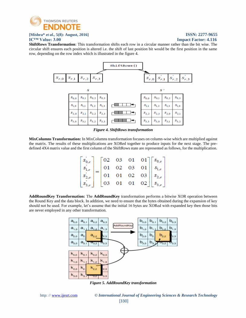
ShiftRows Transformation: This transformation shifts each row in a circular manner rather than the bit wise. The
circular shift ensures each position is altered i.e. the shift of last position bit would be the first position in the same
row, depending on the row index which is illustrated in the figure 4.
Figure 4. ShiftRows transformation
MixColumns Transformation: In MixColumns transformation focuses on column-wise which are multiplied against
the matrix. The results of these multiplications are XORed together to produce inputs for the next stage. The pre-
defined 4X4 matrix value and the first column of the ShiftRows state are represented as follows, for the multiplication.
AddRoundKey Transformation: The AddRoundKey transformation performs a bitwise XOR operation between
the Round Key and the data block. In addition, we need to ensure that the bytes obtained during the expansion of key
should not be used. For example, let’s assume that the initial 16 bytes are XORed with expanded key then those bits
are never employed in any other transformation.
Figure 5. AddRoundKey transformation
[Mishra* et al., 5(8): August, 2016] ISSN: 2277-9655
IC™ Value: 3.00 Impact Factor: 4.116
http: // www.ijesrt.com © International Journal of Engineering Sciences & Research Technology
[331]
KEY EXPANSION It is general understanding that the key must be expanded prior to encoding and/or decoding process. Addround Key
transformation discussed in earlier section supports the key expansion that is performed at the initial stage of the
coding process. In general, the expansion of key ensures the size of the key is more than the sub-keys that often
provides enough space for the algorithm. The key size and ExpandedKey size are interrelated and largely depend on
the number of rounds. Most of the key expansions are performed based on few major routines that are executed in
consecutive that are namely
ROT WORD (4 bytes: circular shift)
SUB WORD (4bytes: substitution)
RCON
XOR
DECRYPTION The decoding process is a straightforward process where all necessary parameters are dictated based on the secret key.
The Cipher transformations are simple inverse application of the encoding process at each for the AES algorithm that
are listed below
InvShiftRows
InvSubBytes
InvMixColumns
AddRoundKey
PROPOSED ARCHITECTURE In recent years, various designs were introduced for AES of different key combinations to address security based
applications; unfortunately their robustness and immunity against brute-force are not analyzed but the delays and
power consumption are given priority. The major problem regarding the AES lies with complex transformation that
includes repetitive transformation and shift operations that induce significant delay and require high computation time
to complete the operation thus consuming high power. In terms of hardware engineering, the measure of hardware
design quality and feasibility can be expressed as a function of the issues related with the product i.e. is it has minimum
delay, size, and power consumption and so on.
With significant rise in the demand of the quality in processor, AES based architecture is becoming a popular method
to address such issues of data security. In the last few years, the main motto of the researchers was to enhance speed
of the AES operation in consideration. Each block has several advantages and corresponding limitations, so to obtain
a precise execution at end of each stage we need to focus on the performance of each module. The marking of the
individual module/block based design to investigate various Pipelined transformations to achieve low power
consumption while offering high speed which is prime motivation of this investigation. The feasibility study of the
entire AES modeled on ModelSim depends on three factors i.e. size, power and delay which are calculated for a
transformation stage, thus it helps us in designing high speed AES architecture in an optimized and effective manner.
The state is defined by the block’s current condition and the transformation alters the block at each round.
Implementation Requirements
The proposed system is designed based the advantages on various existing architectures and the quality set to address
complicated problems. As per the outcomes, the constraints are projected with detail implementation requirement was
used for alternative creating and subjective judgments on hardware design. Implementation requirement would
enhance alternative creating and consolidate it with security activity and computational zing soon think about the
interrelations between delays, complexity metrics with repetitiveness, and power consumption.
Data Length Requirements: Any data that could be converted into a bit stream can act as input data for AES
algorithm based implementation but we length is fixed (i.e.128bits). The data length is fixed for both Encoding and
decoding blocks of AES implementation i.e. 128 bits.
Key Length Requirements: In this paper, the key length is fixed to 128-bits but there various key lengths that could
be incorporated.
[Mishra* et al., 5(8): August, 2016] ISSN: 2277-9655
IC™ Value: 3.00 Impact Factor: 4.116
http: // www.ijesrt.com © International Journal of Engineering Sciences & Research Technology
[332]
Keying Restrictions: There are no constraints or restrictions in the selection of the secret key but care has to been
taken while communicating the key among the authorized users.
Parameterization: key length = 128 bits, Nb (size of block) = 4 and Nr = 10.
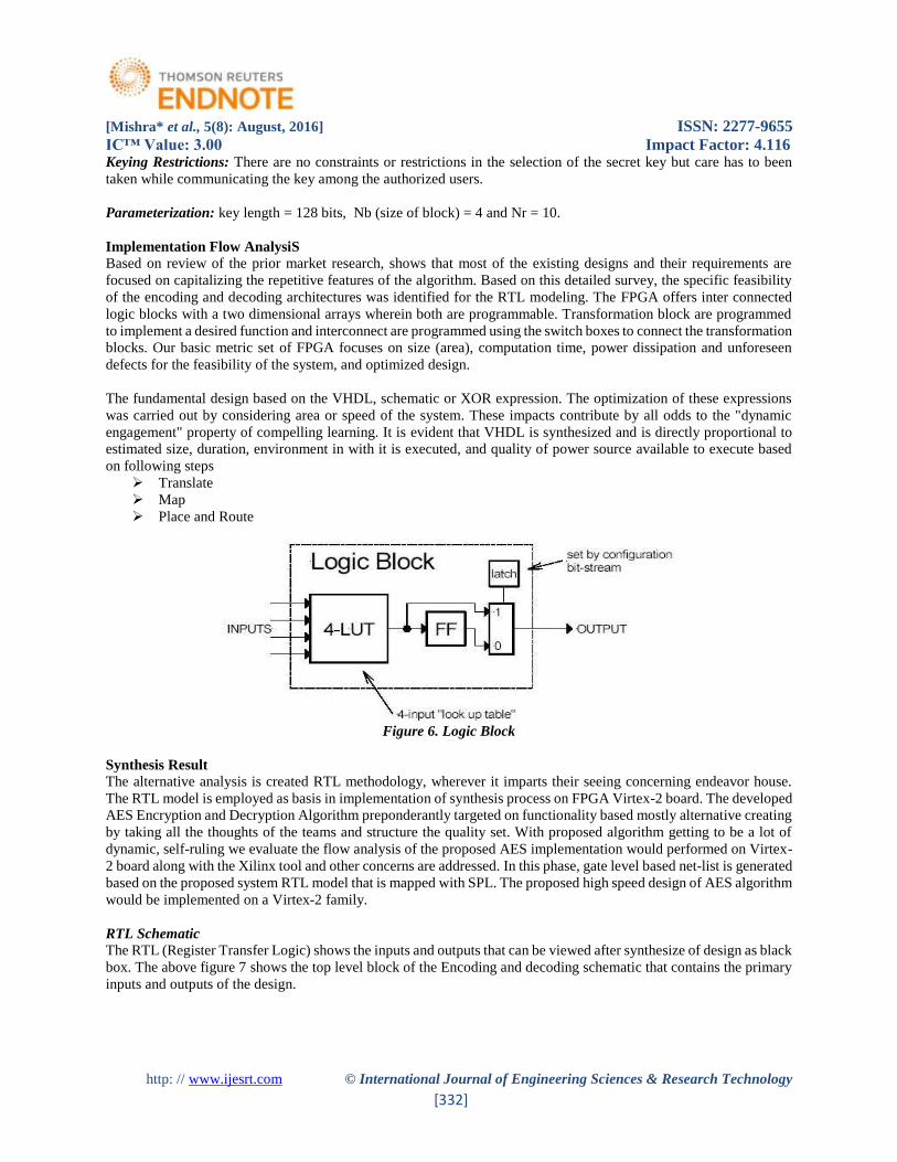
Implementation Flow AnalysiS Based on review of the prior market research, shows that most of the existing designs and their requirements are
focused on capitalizing the repetitive features of the algorithm. Based on this detailed survey, the specific feasibility
of the encoding and decoding architectures was identified for the RTL modeling. The FPGA offers inter connected
logic blocks with a two dimensional arrays wherein both are programmable. Transformation block are programmed
to implement a desired function and interconnect are programmed using the switch boxes to connect the transformation
blocks. Our basic metric set of FPGA focuses on size (area), computation time, power dissipation and unforeseen
defects for the feasibility of the system, and optimized design.
The fundamental design based on the VHDL, schematic or XOR expression. The optimization of these expressions
was carried out by considering area or speed of the system. These impacts contribute by all odds to the "dynamic
engagement" property of compelling learning. It is evident that VHDL is synthesized and is directly proportional to
estimated size, duration, environment in with it is executed, and quality of power source available to execute based
on following steps
Translate
Map
Place and Route
Figure 6. Logic Block
Synthesis Result The alternative analysis is created RTL methodology, wherever it imparts their seeing concerning endeavor house.
The RTL model is employed as basis in implementation of synthesis process on FPGA Virtex-2 board. The developed
AES Encryption and Decryption Algorithm preponderantly targeted on functionality based mostly alternative creating
by taking all the thoughts of the teams and structure the quality set. With proposed algorithm getting to be a lot of
dynamic, self-ruling we evaluate the flow analysis of the proposed AES implementation would performed on Virtex-
2 board along with the Xilinx tool and other concerns are addressed. In this phase, gate level based net-list is generated
based on the proposed system RTL model that is mapped with SPL. The proposed high speed design of AES algorithm
would be implemented on a Virtex-2 family.
RTL Schematic
The RTL (Register Transfer Logic) shows the inputs and outputs that can be viewed after synthesize of design as black
box. The above figure 7 shows the top level block of the Encoding and decoding schematic that contains the primary
inputs and outputs of the design.
[Mishra* et al., 5(8): August, 2016] ISSN: 2277-9655
IC™ Value: 3.00 Impact Factor: 4.116
http: // www.ijesrt.com © International Journal of Engineering Sciences & Research Technology
[333]
Figure 7. RTL Schematic
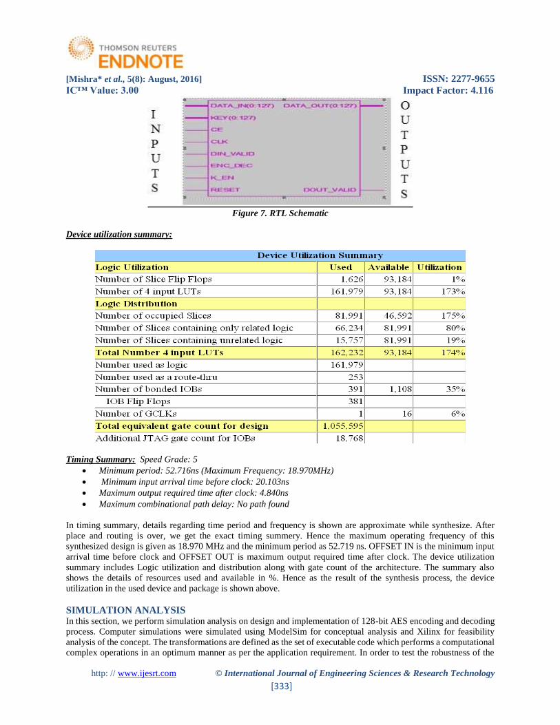
Device utilization summary:
Timing Summary: Speed Grade: 5
Minimum period: 52.716ns (Maximum Frequency: 18.970MHz)
Minimum input arrival time before clock: 20.103ns
Maximum output required time after clock: 4.840ns
Maximum combinational path delay: No path found
In timing summary, details regarding time period and frequency is shown are approximate while synthesize. After
place and routing is over, we get the exact timing summery. Hence the maximum operating frequency of this
synthesized design is given as 18.970 MHz and the minimum period as 52.719 ns. OFFSET IN is the minimum input
arrival time before clock and OFFSET OUT is maximum output required time after clock. The device utilization
summary includes Logic utilization and distribution along with gate count of the architecture. The summary also
shows the details of resources used and available in %. Hence as the result of the synthesis process, the device
utilization in the used device and package is shown above.
SIMULATION ANALYSIS In this section, we perform simulation analysis on design and implementation of 128-bit AES encoding and decoding
process. Computer simulations were simulated using ModelSim for conceptual analysis and Xilinx for feasibility
analysis of the concept. The transformations are defined as the set of executable code which performs a computational
complex operations in an optimum manner as per the application requirement. In order to test the robustness of the
[Mishra* et al., 5(8): August, 2016] ISSN: 2277-9655
IC™ Value: 3.00 Impact Factor: 4.116
http: // www.ijesrt.com © International Journal of Engineering Sciences & Research Technology
[334]
proposed implementation of AES that needs to be modeled in various scenarios and definitions of inputs and key. It
is vital that the outcome of the system needs to be consistent, efficient and reliable based on the key applied within
the application in consideration. Henceforth, Modelsim tool is employed to test the feasibility of the approach with
reference to the functionalities and architecture characteristics of the design. Furthermore, AES based encoding and
decoding operations are performed on fixed key size of 128 bits so as to obtained cipher text that should obscure with
reference to original data which validates that proposed design works in an effective manner and as per the constraints
defined by the algorithm.
Analysis
Initial investigation was based on the test bench that automatically forces random inputs for the process in
consideration. Hence, the proposed system robustness could be measured by evaluating the waveforms for the various
cases associated with the design flow of proposed FPGA architecture. The AES implementation offers inter connected
logic blocks with a two dimensional arrays that perform various complex transformations. The various cases of the
simulation are discussed in detail.
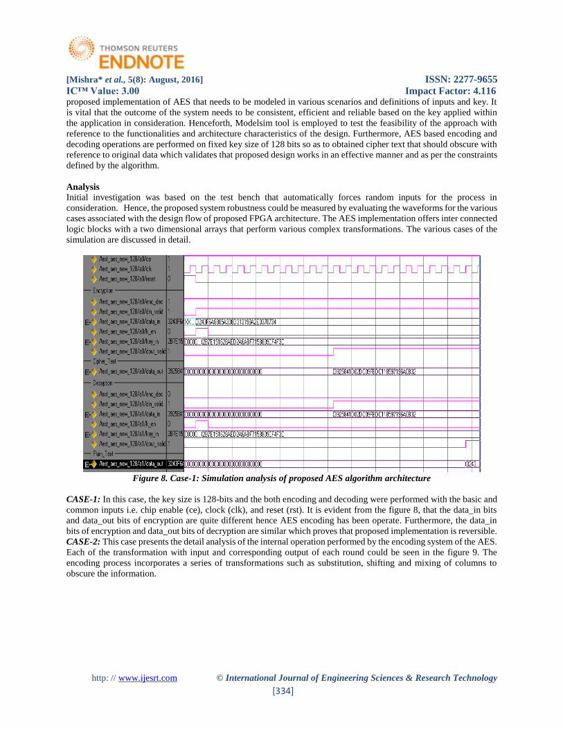
Figure 8. Case-1: Simulation analysis of proposed AES algorithm architecture
CASE-1: In this case, the key size is 128-bits and the both encoding and decoding were performed with the basic and
common inputs i.e. chip enable (ce), clock (clk), and reset (rst). It is evident from the figure 8, that the data_in bits
and data_out bits of encryption are quite different hence AES encoding has been operate. Furthermore, the data_in
bits of encryption and data_out bits of decryption are similar which proves that proposed implementation is reversible.
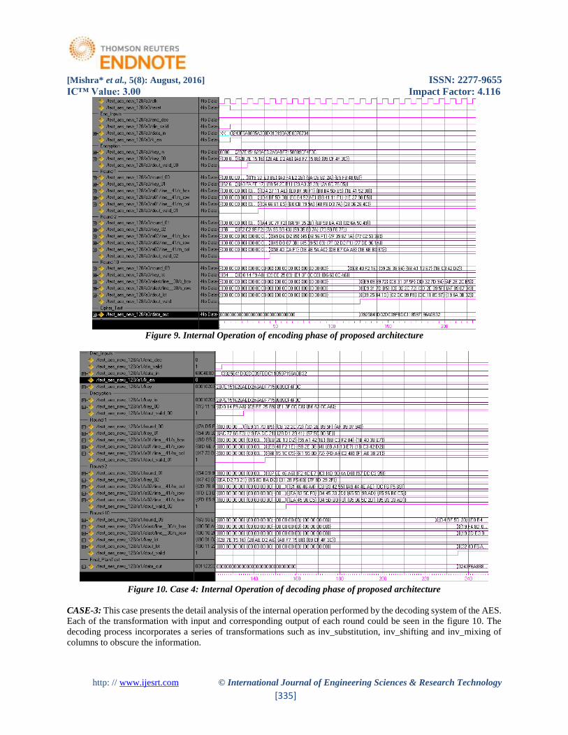
CASE-2: This case presents the detail analysis of the internal operation performed by the encoding system of the AES.
Each of the transformation with input and corresponding output of each round could be seen in the figure 9. The
encoding process incorporates a series of transformations such as substitution, shifting and mixing of columns to
obscure the information.
[Mishra* et al., 5(8): August, 2016] ISSN: 2277-9655
IC™ Value: 3.00 Impact Factor: 4.116
http: // www.ijesrt.com © International Journal of Engineering Sciences & Research Technology
[335]
Figure 9. Internal Operation of encoding phase of proposed architecture
Figure 10. Case 4: Internal Operation of decoding phase of proposed architecture
CASE-3: This case presents the detail analysis of the internal operation performed by the decoding system of the AES.
Each of the transformation with input and corresponding output of each round could be seen in the figure 10. The
decoding process incorporates a series of transformations such as inv_substitution, inv_shifting and inv_mixing of
columns to obscure the information.
[Mishra* et al., 5(8): August, 2016] ISSN: 2277-9655
IC™ Value: 3.00 Impact Factor: 4.116
http: // www.ijesrt.com © International Journal of Engineering Sciences & Research Technology
[336]
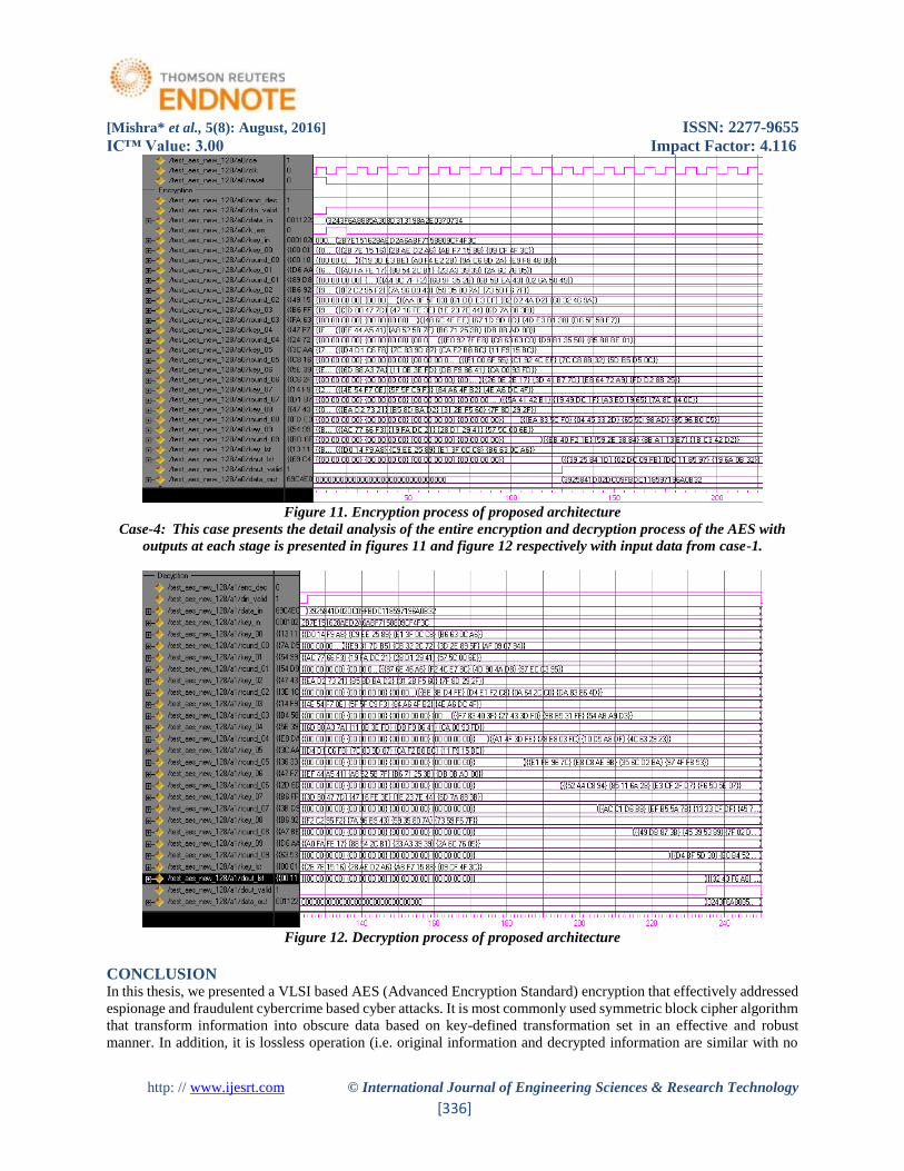
Figure 11. Encryption process of proposed architecture
Case-4: This case presents the detail analysis of the entire encryption and decryption process of the AES with
outputs at each stage is presented in figures 11 and figure 12 respectively with input data from case-1.
Figure 12. Decryption process of proposed architecture
CONCLUSION In this thesis, we presented a VLSI based AES (Advanced Encryption Standard) encryption that effectively addressed
espionage and fraudulent cybercrime based cyber attacks. It is most commonly used symmetric block cipher algorithm
that transform information into obscure data based on key-defined transformation set in an effective and robust
manner. In addition, it is lossless operation (i.e. original information and decrypted information are similar with no
[Mishra* et al., 5(8): August, 2016] ISSN: 2277-9655
IC™ Value: 3.00 Impact Factor: 4.116
http: // www.ijesrt.com © International Journal of Engineering Sciences & Research Technology
[337]
distortion) with size of input and output being the same and could be extended to a wide range of applications. We
limit our focus to128-bit AES encoding and decoding operations over VHDL coded transformation that requires key
for successful completion of the operation
With rise in several methods proposed for implementation of data security it has become more vital for a feasibility
study of any hardware design is essential i.e. to test encryption and decryption process of the proposed 128-bit AES
algorithm. Successful implementation and feasibility analysis of the AES encoding and decoding algorithm are carried
out using ModelSim. In addition, the simulations results prove that the proposed implement offers promising results
in speed and delay in comparison with other schematics. The analysis of the each of the transformation was also
performed based coding on FPGA using Xilinx ISE tool.
REFERENCES [1] Wikipedia: Digital India.
[2] D. Schneier, Applied Cryptography, John Wiley & Son, Inc., New York, NY, 1996.
[3] B. Furht, D. Socek, and A.M. Eskicioglu, “Fundamentals of Multimedia Encryption Techniques,” Chapter
in Multimedia Security Handbook, pp. 94 – 144, CRC Press, 2005
[4] Zhang, X., & Parhi, K. K. (2004). High-speed VLSI architectures for the AES algorithm. IEEE Transactions
on Very Large Scale Integration (VLSI) Systems, 12(9), 957-967.
[5] Gnanambika, M., Adilakshmi, S., & Noorbasha, D. F. (2012). AES-128 Bit Algorithm Using Fully Pipelined
Architecture for Secret Communication.International Journal of Engineering Research and
Applications, 3(2), 166-169
[6] Kalaiselvi, K., & Mangalam, H. (2015). Power efficient and high performance VLSI architecture for AES
algorithm. Journal of Electrical Systems and Information Technology, 2(2), 178-183.
[7] Das, S. S., & Resmi, R. (2014, December). An efficient VLSI implementation of AES encryption using ROM
submodules and exclusion of shiftrows. InComputational Systems and Communications (ICCSC), 2014 First
International Conference on (pp. 248-251). IEEE.
[8] Dattathreya, K. A., & Kashwan, K. R. (2015). VLSI Implementation of 400 MHz 128-Bit Low Power
Montgomery Multiplier for AES Algorithm. Journal of Next Generation Information Technology, 6(1), 10.
[9] Meera, R., & Kalaiselvi, K. (2016). Design and Implementation of Low Power and High Performance AES
Algorithm using FPGA. Wireless Communication, 8(6), 257-259.
[10] Vaidehi, M., & Rabi, B. J. (2015). Enhanced MixColumn Design for AES Encryption. Indian Journal of
Science and Technology, 8(35).
[11] Zhang, Q., Cao, J., Yu, D., Cao, X., Zhang, X., Ye, Y., & Chen, B. (2015, June). A low-energy high-
throughput asynchronous AES for secure smart cards. In Electron Devices and Solid-State Circuits (EDSSC),
2015 IEEE International Conference on (pp. 487-490). IEEE.
[12] Kshirsagar, R. V., & Vyawahare, M. V. (2012, November). FPGA implementation of high speed VLSI
architectures for AES algorithm. In 2012 Fifth International Conference on Emerging Trends in Engineering
and Technology (pp. 239-242). IEEE.
[13] Sklavos, N., & Koufopavlou, O. (2002). Architectures and VLSI implementations of the AES-proposal
Rijndael. IEEE Transactions on Computers, 51(12), 1454-1459.
[14] Kumar, S., Sharma, V. K., & Mahapatra, K. K. (2013, March). Low latency VLSI architecture of S-box for
AES encryption. In Circuits, Power and Computing Technologies (ICCPCT), 2013 International Conference
on (pp. 694-698). IEEE
[15] Bajaj, R. D., Gokhale, U. M., & VLSI, M. T. (2016). Design and Simulation of AES Algorithm for
Cryptography. International Journal of Engineering Science, 6340.
[16] Shan, W., Zhang, X., Fu, X., & Cao, P. (2014). VLSI design of a reconfigurable S-box based on memory
sharing method. IEICE Electronics Express, 11(1), 20130872-20130872.
[17] Panigrahi, S., Sharma, V. K., Das, C., & Mahapatra, K. K. (2013, March). Efficient VLSI architecture of
medium throughput AES encryption. In 2013 International Conference on Circuits, Power and Computing
Technologies (ICCPCT).
[18] Mohanty, J. P. (2014). VLSI implementation for security paradigm of AES including DPA attacks (Doctoral
dissertation, National Institute of Technology Rourkela)