Embed Size (px)
Citation preview
Mem. S.A.It. Vol. 88, 186c© SAIt 2017 Memorie della
Design and implementation of projects withXilinx Zynq FPGA: a practical case
R. Travaglini1, I. D’Antone1, S. Meneghini1, L. Rignanese1,2, and M. Zuffa1
1 Istituto Nazionale di Fisica Nucleare – Sezione di Bologna, Viale C. Berti Pichat 6/2, 40127Bologna, Italy, e-mail: [email protected]
2 Universita di Bologna, Dipartimento di Fisica e Astronomia, viale C. Berti Pichat 6/2, 40127Bologna, Italy
Abstract. The main advantage when using FPGAs with embedded processors is the availabil-ity of additional several high-performance resources in the same physical device. Moreover,the FPGA programmability allows for connect custom peripherals. Xilinx have designed aprogrammable device named Zynq-7000 (simply called Zynq in the following), which inte-grates programmable logic (identical to the other Xilinx “serie 7” devices) with a System onChip (SOC) based on two embedded ARM R©processors. Since both parts are deeply connected,the designers benefit from performance of hardware SOC and flexibility of programmabilityas well. In this paper a design developed by the Electronic Design Department at the BolognaDivision of INFN will be presented as a practical case of project based on Zynq device. It is de-veloped by using a commercial board called ZedBoard hosting a FMC mezzanine with a 12-bit500 MS/s ADC. The Zynq FPGA on the ZedBoard receives digital outputs from the ADC andsend them to the acquisition PC, after proper formatting, through a Gigabit Ethernet link. Themajor focus of the paper will be about the methodology to develop a Zynq-based design withthe Xilinx Vivado software, enlightening how to configure the SOC and connect it with theprogrammable logic. Firmware design techniques will be presented: in particular both VHDLand IP core based strategies will be discussed. Further, the procedure to develop software forthe embedded processor will be presented. Finally, some debugging tools, like the embeddedLogic Analyzer, will be shown. Advantages and disadvantages with respect to adopting FPGAwithout embedded processors will be discussed.
Key words. System on Chip - Firmware - Embedded Software - Acquisition System
1. Introduction
The project described in this paper consists ina printed circuit board (PCB) realizing one ac-quisition channel running at 1 GS/s. It is builtusing only commercial devices. This projecthas been developed by the Electronic DesignDepartment at the Bologna Division of theItalian National Institute for Nuclear Physics
(INFN). This task is a feasibility study to copewith future requests from the experiments andfollows a previous experience when a 500MS/s board was built. Such a fast acquisi-tion rate allows for better performances both inpulse shape discrimination and pile-up rejec-tion,especially when using detectors with fastresponse (for instance Silicon PhotoMultiplierand fast Scintillators with rising times of the
Travaglini: Xilinx Zynq, a practical case 187
order of 10 ns). In the following, after ashort presentation of the Electronic DesignDepartment and its experience on designingwith FPGA, the project is briefly introduced.
1.1. The Electronic Design Departmentat the Bologna Division of INFN:FPGA-related activity andexperience
The Electronic Department has to provide sup-port to all the electronics activity performed inthe INFN Bologna Division. Its tasks are thedesign, the development and the installationof electronic devices for the front-end, triggerand acquisition systems of particle physics ex-periment. It is composed by 14 members withseveral distinct professional qualifications andskills. Concerning the FPGA, the ElectronicDepartment has a twentyfold experience on us-ing programmable devices of the major firms(Altera, Microsemi, Xilinx). It deals with everyFPGA-related aspect : PCB design, firmwaredevelopment and design of software for em-bedded microprocessors. Several software ap-plications are used to design, simulate andverify the boards: for instance Orcad fromCadence and Pads, Expedition and Hyperlynkfrom Mentor. The firmware is designed by us-ing several programming languages: mainlyVHDL but also C, C++ and Handel-C as well.Test and control software is mainly developedwith C and C++.
1.2. R&D design: a 1GS/s interleavedADC
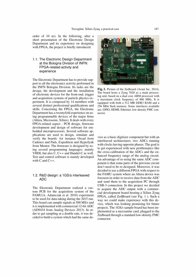
The Electronic Department realized a cus-tom PCB for the acquisition system of theFAMU(A. Adamczak et al. 2016) experimentto be used for data-taking during the 2015 run.This board can sample signals at 500 MS/s andit is implemented with commercial 12-bit ADC(AD9434 from Analog Devices 2013). In or-der to get sampling at a double rate, it was de-cided to build a system which had the same de-
Fig. 1. Picture of the Zedboard (Avnet Inc. 2014).The board hosts a Zynq 7020 as a main process-ing unit, based on a dual core ARM processor witha maximum clock frequency of 866 MHz. It isequipped with both a 512 MB DDR3 RAM and a256 Mbit flash memory. Some interfaces availableare: GPIO, HDMI, Ethernet, low-density FMC con-nector.
vice as a basic digitizer component but with aninterleaved architectures: two ADCs runningwith clocks having opposite phases. The goal isto get experienced with new problematics likethe cross-calibration of the ADCs and the en-hanced frequency range of the analog circuit.An advantage of re-using the same ADC com-ponent is that some parts of the previous circuitdon’t need to be re-designed. Moreover, it wasdecided to use a different FPGA with respect tothe FAMU system where an Altera device wasforeseen in order to receive data from the ADCand send them to the acquisition PC throughUSB-3 connection. In this project we decidedto acquire the ADC output with a commer-cial development board hosting a Xilinx ZynqFPGA, called ZedBoard (see Fig. 1 ). Such away we could make experience with this de-vice, which was looking promising for futureprojects. The 1GS/s sample board has been im-plemented as a mezzanine card, plugged to theZedboard through a standard low-density FMCconnector.
188 Travaglini: Xilinx Zynq, a practical case
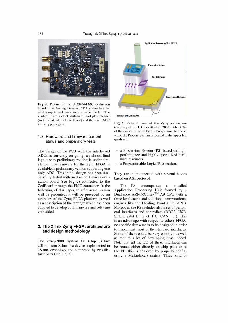
Fig. 2. Picture of the AD9434-FMC evaluationboard from Analog Devices. SDA connectors foranalog inputs and clock are visible on the left. Thevisible IC are a clock distributor and jitter cleaner(in the center-left of the board) and the main ADCin the upper region.
1.3. Hardware and firmware currentstatus and preparatory tests
The design of the PCB with the interleavedADCs is currently on going: an almost-finallayout with preliminary routing is under sim-ulation. The firmware for the Zynq FPGA isavailable in preliminary version supporting oneonly ADC. This initial design has been suc-cessfully tested with an Analog Devices eval-uation board (see Fig 2) connected to theZedBoard through the FMC connector. In thefollowing of this paper, this firmware versionwill be presented; it will be preceded by anoverview of the Zynq FPGA platform as wellas a description of the strategy which has beenadopted to develop both firmware and softwareembedded.
2. The Xilinx Zynq FPGA: architectureand design methodology
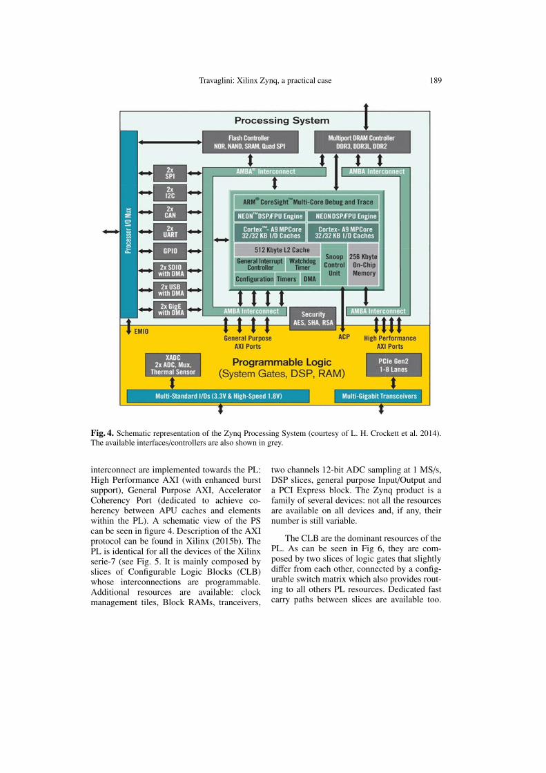
The Zynq-7000 System On Chip (Xilinx2015a) from Xilinx is a device implemented in28 nm technology and composed by two dis-tinct parts (see Fig. 3):
Fig. 3. Pictorial view of the Zynq architecture(courtesy of L. H. Crockett et al. 2014). About 3/4of the device is in use by the Programmable Logic,while the Process System is located in the upper leftquadrant.
– a Processing System (PS) based on high-performance and highly specialized hard-ware resources;
– a Programmable Logic (PL) section.
They are interconnected with several bussesbased on AXI protocol.
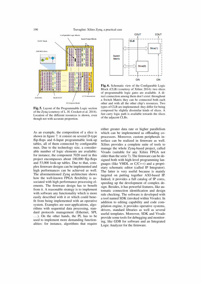
The PS encompasses a so-calledApplication Processing Unit formed by aDual-core ARM R©CortexTM-A9 CPU with athree level cache and additional computationalengines like the Floating Point Unit (APU).Moreover, the PS includes also a set of periph-eral interfaces and controllers (DDR3, USB,SPI, Gigabit Ethernet, I2C, CAN, . . . ). Thisis an advantage with respect to others FPGA:no specific firmware is to be designed in orderto implement most of the standard interfaces.Some of them could be very complex as wellas require a lot of developing time indeed.Note that all the I/O of these interfaces canbe routed either directly on chip pads or tothe PL; this is achieved by properly config-uring a Multiplexers matrix. Three kind of
Travaglini: Xilinx Zynq, a practical case 189
Fig. 4. Schematic representation of the Zynq Processing System (courtesy of L. H. Crockett et al. 2014).The available interfaces/controllers are also shown in grey.
interconnect are implemented towards the PL:High Performance AXI (with enhanced burstsupport), General Purpose AXI, AcceleratorCoherency Port (dedicated to achieve co-herency between APU caches and elementswithin the PL). A schematic view of the PScan be seen in figure 4. Description of the AXIprotocol can be found in Xilinx (2015b). ThePL is identical for all the devices of the Xilinxserie-7 (see Fig. 5. It is mainly composed byslices of Configurable Logic Blocks (CLB)whose interconnections are programmable.Additional resources are available: clockmanagement tiles, Block RAMs, tranceivers,
two channels 12-bit ADC sampling at 1 MS/s,DSP slices, general purpose Input/Output anda PCI Express block. The Zynq product is afamily of several devices: not all the resourcesare available on all devices and, if any, theirnumber is still variable.
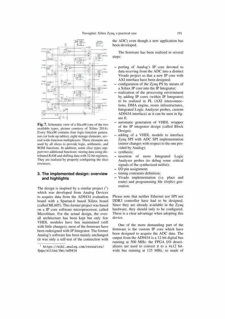
The CLB are the dominant resources of thePL. As can be seen in Fig 6, they are com-posed by two slices of logic gates that slightlydiffer from each other, connected by a config-urable switch matrix which also provides rout-ing to all others PL resources. Dedicated fastcarry paths between slices are available too.
190 Travaglini: Xilinx Zynq, a practical case
Fig. 5. Layout of the Programmable Logic sectionof the Zynq (courtesy of L. H. Crockett et al. 2014).Location of the different resources is shown, eventhough not with accurate proportion.
As an example, the composition of a slice isshown in figure 7: it consist on several D-typeflip-flops and 6-Input programmable look-uptables, all of them connected by configurablemux. Due to the technology size, a consider-able number of logic elements are available:for instance, the component 7020 used in thisproject encompasses about 100,000 flip-flopsand 53,000 look-up tables. Due to that, com-plex firmware designs can be implemented andhigh performances can be achieved as well.The aforementioned Zynq architecture showshow the well-known FPGA flexibility is as-sociated with high performance processing el-ements. The firmware design has to benefitfrom it. A reasonable strategy is to implementwith software any functionality which is moreeasily described with it or which could bene-fit from being implemented with an operativesystem. Examples are user-applications, algo-rithms with sequential data processing, stan-dard protocols management (Ethernet, SPI,. . . ). On the other hands, the PL has to beused to implement more demanding function-alities: for instance, algorithms that require
Fig. 6. Schematic view of the Configurable LogicBlock (CLB) (courtesy of Xilinx 2014): two slicesof programmable logic gates are available. A di-rect connection among them don’t exist: throughouta Switch Matrix they can be connected both eachother and with all the other chip’s resources. Twotypes of CLB are implemented: they differ for beingcomposed by slightly dissimilar kinds of slices. Afast carry logic path is available towards the slicesof the adjacent CLBs.
either greater data rate or higher parallelismwhich can be implemented as offloading co-processors. Moreover, custom peripherals in-terface can be realized in firmware as well.Xilinx provides a complete suite of tools tomanage the whole Zynq-based project, calledVivado (suitable for any Xilinx FPGA notolder than the serie 7). The firmware can be de-signed both with high-level programming lan-guages (like VHDL or C/C++) and a propri-etary schematic editor (called IP Integrator).The latter is very useful because is mainlytargeted on putting together AXI-based IP.Indeed, it provides a full catalog of IP cores,speeding up the development of complex de-sign. Besides, it has powerful features, like au-tomatic connection identification and designrule checking. The software is developed witha tool named SDK (invoked within Vivado). Inaddition to editing capability and code com-pilation engine, it provides operative systems,drivers, standard libraries as well as severaluseful templates. Moreover, SDK and Vivadoprovide some tools for debugging and monitor-ing, like GDB for software and an IntegratedLogic Analyzer for the firmware.
Travaglini: Xilinx Zynq, a practical case 191
Fig. 7. Schematic view of a SliceM (one of the twoavailable types, picture courtesy of Xilinx 2014).Every SliceM contains four logic-function genera-tors (or look-up tables), eight storage elements, sev-eral wide-function multiplexers. These elements areused by all slices to provide logic, arithmetic, andROM functions. In addition, some slice types sup-port two additional functions: storing data using dis-tributed RAM and shifting data with 32-bit registers.They are realized by properly configuring the sliceresources.
3. The implemented design: overviewand highlights
The design is inspired by a similar project (1)which was developed from Analog Devicesto acquire data from the AD9434 evaluationboard with a Spartan-6 based Xilinx board(called ML605). This former project was basedon a IP core software microprocessor, calledMicroblaze. For the actual design, the over-all architecture has been kept but only fewVHDL modules have ben maintained (stillwith little changes); most of the firmware havebeen redesigned with IP Integrator. The formerAnalog’s software has been mainly unchanged(it was only a self-test of the connection with
1 https://wiki.analog.com/resources/fpga/xilinx/fmc/ad9434
the ADC) even though a new application hasbeen developed.
The firmware has been realized in severalsteps:
– porting of Analog’s IP core devoted todata receving from the ADC into a distinctVivado project so that a new IP core withAXI interface have been designed;
– configuration of the Zynq PS by means ofa Xilinx IP core into the IP Integrator;
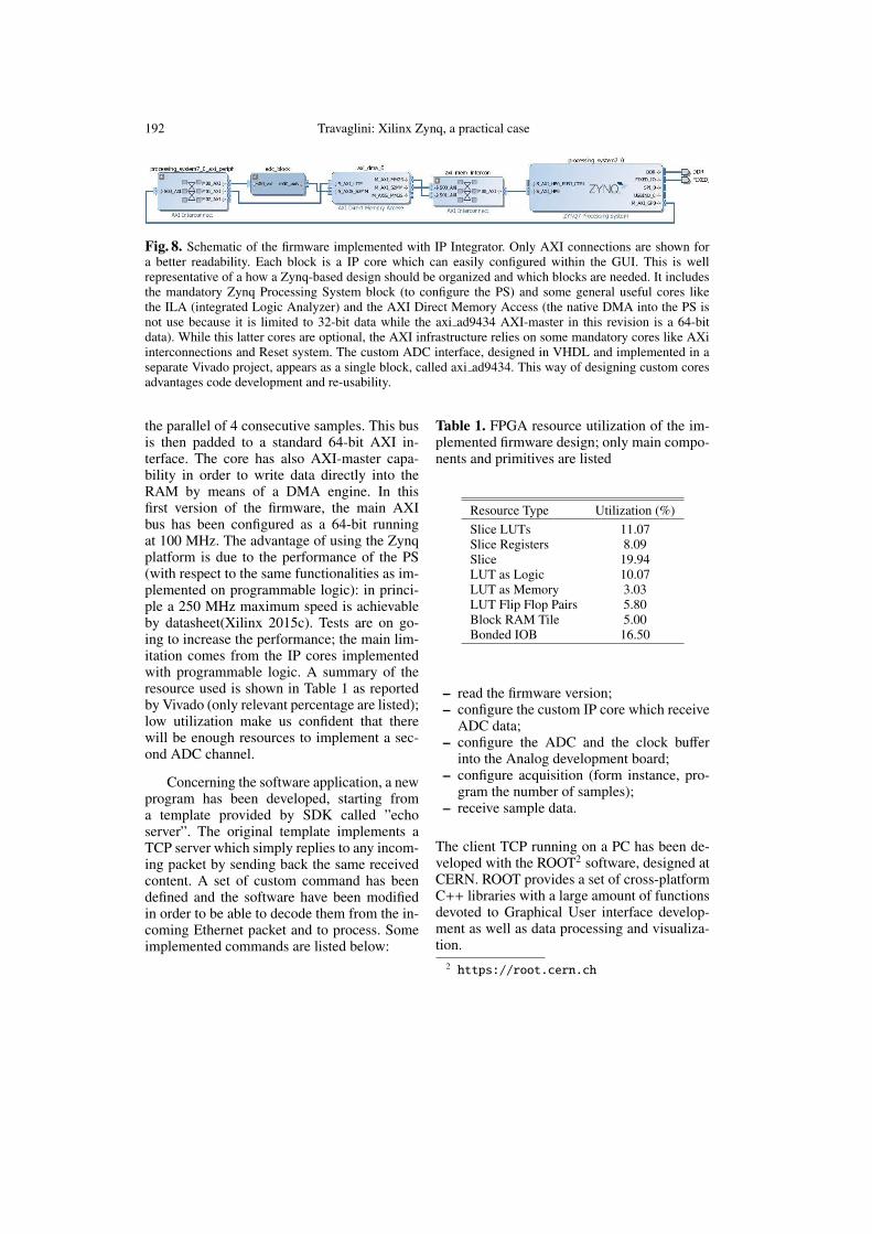
– realization of the processing environmentby adding IP cores (within IP Integrator)to be realized in PL (AXI interconnec-tions, DMA engine, resets infrastructures,Integrated Logic Analyzer probes, customAD9434 interface) as it can be seen in fig-ure 8;
– automatic generation of VHDL wrapperof the IP integrator design (called BlockDesign);
– adding of a VHDL module to interfaceZynq SPI with ADC SPI implementation(minor changes with respect to the one pro-vided by Analog);
– synthesis;– insertion of more Integrated Logic
Analyzer probes (to debug some criticalsignals of the synthesized netlist);
– I/O pin assignment;– timing contraints definition;– Vivado implementation (i.e. place and
route) and programming file (bitfile) gen-eration.
Please note that neither Ethernet nor SPI norDDR3 controller have had to be designed.Since they are already available in the Zynqhardware, they should only to be configured.These is a clear advantage when adopting thisdevice.
One of the more demanding part of thefirmware is the custom IP core which havebeen designed to acquire the ADC data. Theoutput from the AD9434 is a 12-bit digital busrunning at 500 MHz: the FPGA I/O deseri-alizers are used to convert it to a 4x12 bit-wide bus running at 125 MHz, so made of
192 Travaglini: Xilinx Zynq, a practical case
Fig. 8. Schematic of the firmware implemented with IP Integrator. Only AXI connections are shown fora better readability. Each block is a IP core which can easily configured within the GUI. This is wellrepresentative of a how a Zynq-based design should be organized and which blocks are needed. It includesthe mandatory Zynq Processing System block (to configure the PS) and some general useful cores likethe ILA (integrated Logic Analyzer) and the AXI Direct Memory Access (the native DMA into the PS isnot use because it is limited to 32-bit data while the axi ad9434 AXI-master in this revision is a 64-bitdata). While this latter cores are optional, the AXI infrastructure relies on some mandatory cores like AXiinterconnections and Reset system. The custom ADC interface, designed in VHDL and implemented in aseparate Vivado project, appears as a single block, called axi ad9434. This way of designing custom coresadvantages code development and re-usability.
the parallel of 4 consecutive samples. This busis then padded to a standard 64-bit AXI in-terface. The core has also AXI-master capa-bility in order to write data directly into theRAM by means of a DMA engine. In thisfirst version of the firmware, the main AXIbus has been configured as a 64-bit runningat 100 MHz. The advantage of using the Zynqplatform is due to the performance of the PS(with respect to the same functionalities as im-plemented on programmable logic): in princi-ple a 250 MHz maximum speed is achievableby datasheet(Xilinx 2015c). Tests are on go-ing to increase the performance; the main lim-itation comes from the IP cores implementedwith programmable logic. A summary of theresource used is shown in Table 1 as reportedby Vivado (only relevant percentage are listed);low utilization make us confident that therewill be enough resources to implement a sec-ond ADC channel.
Concerning the software application, a newprogram has been developed, starting froma template provided by SDK called ”echoserver”. The original template implements aTCP server which simply replies to any incom-ing packet by sending back the same receivedcontent. A set of custom command has beendefined and the software have been modifiedin order to be able to decode them from the in-coming Ethernet packet and to process. Someimplemented commands are listed below:
Table 1. FPGA resource utilization of the im-plemented firmware design; only main compo-nents and primitives are listed
Resource Type Utilization (%)Slice LUTs 11.07Slice Registers 8.09Slice 19.94LUT as Logic 10.07LUT as Memory 3.03LUT Flip Flop Pairs 5.80Block RAM Tile 5.00Bonded IOB 16.50
– read the firmware version;– configure the custom IP core which receive
ADC data;– configure the ADC and the clock buffer
into the Analog development board;– configure acquisition (form instance, pro-
gram the number of samples);– receive sample data.
The client TCP running on a PC has been de-veloped with the ROOT2 software, designed atCERN. ROOT provides a set of cross-platformC++ libraries with a large amount of functionsdevoted to Graphical User interface develop-ment as well as data processing and visualiza-tion.
2 https://root.cern.ch
Travaglini: Xilinx Zynq, a practical case 193
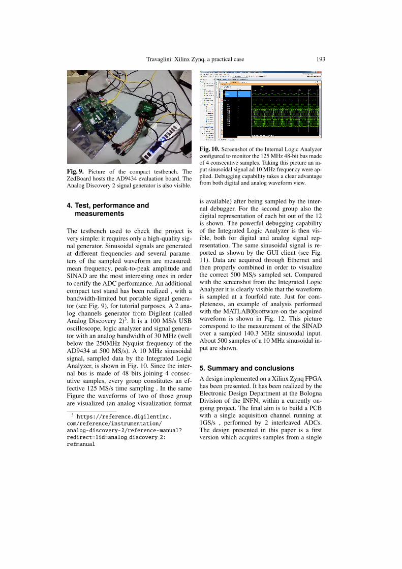
Fig. 9. Picture of the compact testbench. TheZedBoard hosts the AD9434 evaluation board. TheAnalog Discovery 2 signal generator is also visible.
4. Test, performance andmeasurements
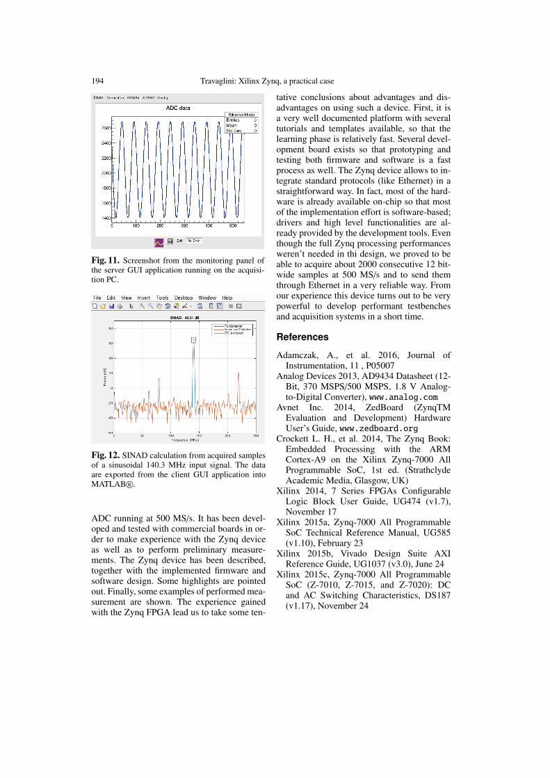
The testbench used to check the project isvery simple: it requires only a high-quality sig-nal generator. Sinusoidal signals are generatedat different frequencies and several parame-ters of the sampled waveform are measured:mean frequency, peak-to-peak amplitude andSINAD are the most interesting ones in orderto certify the ADC performance. An additionalcompact test stand has been realized , with abandwidth-limited but portable signal genera-tor (see Fig. 9), for tutorial purposes. A 2 ana-log channels generator from Digilent (calledAnalog Discovery 2)3. It is a 100 MS/s USBoscilloscope, logic analyzer and signal genera-tor with an analog bandwidth of 30 MHz (wellbelow the 250MHz Nyquist frequency of theAD9434 at 500 MS/s). A 10 MHz sinusoidalsignal, sampled data by the Integrated LogicAnalyzer, is shown in Fig. 10. Since the inter-nal bus is made of 48 bits joining 4 consec-utive samples, every group constitutes an ef-fective 125 MS/s time sampling . In the sameFigure the waveforms of two of those groupare visualized (an analog visualization format
3 https://reference.digilentinc.com/reference/instrumentation/analog-discovery-2/reference-manual?redirect=1id=analog discovery 2:refmanual
Fig. 10. Screenshot of the Internal Logic Analyzerconfigured to monitor the 125 MHz 48-bit bus madeof 4 consecutive samples. Taking this picture an in-put sinusoidal signal ad 10 MHz frequency were ap-plied. Debugging capability takes a clear advantagefrom both digital and analog waveform view.
is available) after being sampled by the inter-nal debugger. For the second group also thedigital representation of each bit out of the 12is shown. The powerful debugging capabilityof the Integrated Logic Analyzer is then vis-ible, both for digital and analog signal rep-resentation. The same sinusoidal signal is re-ported as shown by the GUI client (see Fig.11). Data are acquired through Ethernet andthen properly combined in order to visualizethe correct 500 MS/s sampled set. Comparedwith the screenshot from the Integrated LogicAnalyzer it is clearly visible that the waveformis sampled at a fourfold rate. Just for com-pleteness, an example of analysis performedwith the MATLAB R©software on the acquiredwaveform is shown in Fig. 12. This picturecorrespond to the measurement of the SINADover a sampled 140.3 MHz sinusoidal input.About 500 samples of a 10 MHz sinusoidal in-put are shown.
5. Summary and conclusionsA design implemented on a Xilinx Zynq FPGAhas been presented. It has been realized by theElectronic Design Department at the BolognaDivision of the INFN, within a currently on-going project. The final aim is to build a PCBwith a single acquisition channel running at1GS/s , performed by 2 interleaved ADCs.The design presented in this paper is a firstversion which acquires samples from a single
194 Travaglini: Xilinx Zynq, a practical case
Fig. 11. Screenshot from the monitoring panel ofthe server GUI application running on the acquisi-tion PC.
Fig. 12. SINAD calculation from acquired samplesof a sinusoidal 140.3 MHz input signal. The dataare exported from the client GUI application intoMATLAB R©.
ADC running at 500 MS/s. It has been devel-oped and tested with commercial boards in or-der to make experience with the Zynq deviceas well as to perform preliminary measure-ments. The Zynq device has been described,together with the implemented firmware andsoftware design. Some highlights are pointedout. Finally, some examples of performed mea-surement are shown. The experience gainedwith the Zynq FPGA lead us to take some ten-
tative conclusions about advantages and dis-advantages on using such a device. First, it isa very well documented platform with severaltutorials and templates available, so that thelearning phase is relatively fast. Several devel-opment board exists so that prototyping andtesting both firmware and software is a fastprocess as well. The Zynq device allows to in-tegrate standard protocols (like Ethernet) in astraightforward way. In fact, most of the hard-ware is already available on-chip so that mostof the implementation effort is software-based;drivers and high level functionalities are al-ready provided by the development tools. Eventhough the full Zynq processing performancesweren’t needed in thi design, we proved to beable to acquire about 2000 consecutive 12 bit-wide samples at 500 MS/s and to send themthrough Ethernet in a very reliable way. Fromour experience this device turns out to be verypowerful to develop performant testbenchesand acquisition systems in a short time.
References
Adamczak, A., et al. 2016, Journal ofInstrumentation, 11 , P05007
Analog Devices 2013, AD9434 Datasheet (12-Bit, 370 MSPS/500 MSPS, 1.8 V Analog-to-Digital Converter), www.analog.com
Avnet Inc. 2014, ZedBoard (ZynqTMEvaluation and Development) HardwareUser’s Guide, www.zedboard.org
Crockett L. H., et al. 2014, The Zynq Book:Embedded Processing with the ARMCortex-A9 on the Xilinx Zynq-7000 AllProgrammable SoC, 1st ed. (StrathclydeAcademic Media, Glasgow, UK)
Xilinx 2014, 7 Series FPGAs ConfigurableLogic Block User Guide, UG474 (v1.7),November 17
Xilinx 2015a, Zynq-7000 All ProgrammableSoC Technical Reference Manual, UG585(v1.10), February 23
Xilinx 2015b, Vivado Design Suite AXIReference Guide, UG1037 (v3.0), June 24
Xilinx 2015c, Zynq-7000 All ProgrammableSoC (Z-7010, Z-7015, and Z-7020): DCand AC Switching Characteristics, DS187(v1.17), November 24