Embed Size (px)
Citation preview
International Journal of Engineering and Technology Volume 2 No. 1, January, 2012
ISSN: 2049-3444 © 2011 – IJET Publications UK. All rights reserved. 9
Design and Minimization of Reversible Circuits for a Data Acquisition
and Storage System
1Lafifa Jamal,
2Farah Sharmin,
3Md. Abdul Mottalib,
4Hafiz Md. Hasan Babu
1,2,4Department. of Computer Science & Engineering, University of Dhaka, Dhaka-1000, Bangladesh
3Department of Computer Science and Information Technology
Islamic University of Technology, Gazipur-1704, Dhaka, Bangladesh
ABSTRACT
Reducing power dissipation is the ultimate objective in the world of VLSI circuit design. Conventional logic dissipates more
power by losing bits of information whereas reversibility recovers bit loss from the unique input-output mapping. Thus
reversible logic has become immensely popular research area and its applications have spread in various technologies. In this
paper we have proposed the compact design of reversible circuits for a data acquisition and storage system. The design
comprises with a compact reversible analog-to- digital converter and a reversible address register. In the way of designing this
data acquisition and storage system we have proposed a reversible J-K flip-flop with asynchronous inputs, a reversible D flip-
flop and a reversible three state buffer register. All the reversible designs individually have less number of gates, garbage
outputs and quantum cost compared with the existing ones and have outperformed those described in the literature. Moreover
we have proposed some lower bounds for designing these reversible components of the compact data acquisition and storage
system.
Key words: Reversible Logic, Garbage Output, Flip-Flop, Quantum Cost
1. INTRODUCTION
Reversible logic has spread its popularity in numerous
technologies such as low power CMOS design, optical
information processing, DNA computing, bioinformatics,
quantum computing[1],thermodynamics and
nanotechnology over the last couple of years[2, 3, 4]. In
the early 1960s R. Landauer demonstrated that losing bits
of information causes loss of energy [5]. It is proved that
the loss of each bit of information loses at least KT × ln2
joules of energy where K is the Boltzmann’s constant and
T is the temperature at which the system is operating [5].
Information is lost when an input cannot be recovered
from its output or vice-versa. Reversible logic has the
feature to generate one to one correspondence between its
input and output [6,7,8]. As a result no information is lost
in reversible logic and zero power dissipation would be
achieved only if the network consists of reversible gates
[9]. Synthesis of reversible logic is more complicated than
irreversible one as it imposes many design constraints [6].
A reversible circuit therefore should have the following
attributes [7]:
Since garbage outputs are not used as primary
outputs so any realization technique should
keep garbage as minimum as possible.
Each reversible gate has a particular quantum
cost so any realization technique should keep
the number of reversible gates as minimum as
possible.
Input lines that are either 0 or 1 known as
constant inputs should be as minimum as
possible.
A reversible data acquisition and storage system consists
of a reversible analog-to digital converter which will
convert analog signal into digital form, a reversible
Random Access Memory (RAM) which is a two
dimensional array of memory cells and a reversible
synchronous counter which will point to the consecutive
locations of memory. With the help of theorems and
comparisons the efficiency of reversible logic synthesis of
data acquisition and storage system has also been proved
in this paper.
The paper consists of the following sections: Section 2
describes about the reversible gate, some basic definition
and quantum realization of some reversible circuits.
Section 3 introduces the logic synthesis of reversible data
acquisition and storage system and comparison with other
existing researches. Finally the paper is concluded with the
section 4.
International Journal of Engineering and Technology (IJET) – Volume 2 No. 1, January, 2012
ISSN: 2049-3444 © 2011 – IJET Publications UK. All rights reserved. 10
2. BACKGROUND
In this section we have presented some definitions and
basic idea on reversible logic for our future reference.
Quantum realization of some popular reversible circuits
has also been illustrated in this section.
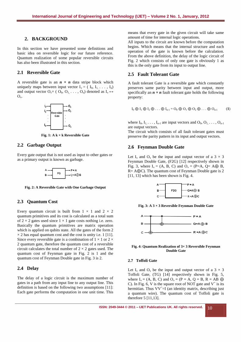
2.1 Reversible Gate
A reversible gate is an n × n data stripe block which
uniquely maps between input vector Iv = ( I0, I1, . . . , In)
and output vector Ov= ( O0, O1, . . . , On) denoted as Iv ↔
Ov.
Fig. 1: A k × k Reversible Gate
2.2 Garbage Output
Every gate output that is not used as input to other gates or
as a primary output is known as garbage.
Fig. 2: A Reversible Gate with One Garbage Output
2.3 Quantum Cost
Every quantum circuit is built from 1 × 1 and 2 × 2
quantum primitives and its cost is calculated as a total sum
of 2 × 2 gates used since 1 × 1 gate costs nothing i.e. zero.
Basically the quantum primitives are matrix operation
which is applied on qubits state. All the gates of the form 2
× 2 has equal quantum cost and the cost is unity i.e. 1 [11].
Since every reversible gate is a combination of 1 × 1 or 2 ×
2 quantum gate, therefore the quantum cost of a reversible
circuit calculates the total number of 2 × 2 gates used. The
quantum cost of Feynman gate in Fig. 2 is 1 and the
quantum cost of Feynman Double gate in Fig. 3 is 2.
2.4 Delay
The delay of a logic circuit is the maximum number of
gates in a path from any input line to any output line. This
definition is based on the following two assumptions [11]:
Each gate performs the computation in one unit time. This
means that every gate in the given circuit will take same
amount of time for internal logic operations.
All inputs to the circuit are known before the computation
begins. Which means that the internal structure and each
operation of the gate is known before the calculation.
From the above definition, the delay of the logic circuit of
Fig. 2 which consists of only one gate is obviously 1 as
this is the only gate from its input to output line.
2.5 Fault Tolerant Gate
A fault tolerant Gate is a reversible gate which constantly
preserves same parity between input and output, more
specifically an n × n fault tolerant gate holds the following
property:
I0 ⊕ I1 ⊕ I2 ⊕ . . . ⊕ In-1 = O0 ⊕ O1 ⊕ O2 ⊕ . . . ⊕ On-1
(1)
where I0, I1, . . . , In-1 are input vectors and O0, O1, . . . , On-1
are output vectors.
The circuit which consists of all fault tolerant gates must
preserve the parity pattern in its input and output vectors.
2.6 Feynman Double Gate
Let Iv and Ov be the input and output vector of a 3 × 3
Feynman Double Gate, (F2G) [12] respectively shown in
Fig. 3, where Iv = (A, B, C) and Ov = (P=A, Q= A⊕ B,
R= A⊕C). The quantum cost of Feynman Double gate is 2
[11, 13] which has been shown is Fig. 4.
Fig. 3: A 3 × 3 Reversible Feynman Double Gate
Fig. 4: Quantum Realization of 3× 3 Reversible Feynman
Double Gate
2.7 Toffoli Gate
Let Iv and Ov be the input and output vector of a 3 × 3
Toffoli Gate, (TG) [14] respectively shown in Fig. 5,
where Iv = (A, B, C) and Ov = (P = A, Q = B, R = AB ⊕
C). In Fig. 6, V is the square root of NOT gate and V+ is its
hermitian. Thus VV+=I (an identity matrix, describing just
a quantum wire). The quantum cost of Toffoli gate is
therefore 5 [11,13].
International Journal of Engineering and Technology (IJET) – Volume 2 No. 1, January, 2012
ISSN: 2049-3444 © 2011 – IJET Publications UK. All rights reserved. 11
Fig. 5: A 3 × 3 Reversible Toffoli Gate
Fig. 6: Quantum Realization of 3 × 3 Reversible Toffoli Gate
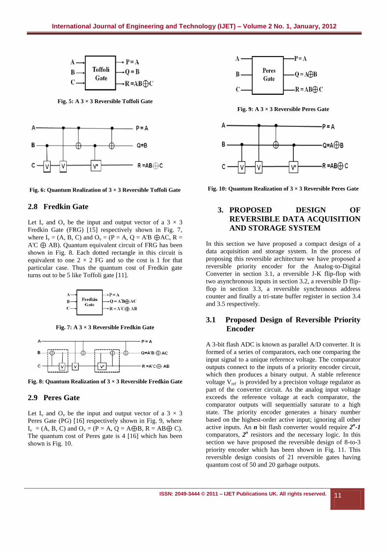
2.8 Fredkin Gate
Let Iv and Ov be the input and output vector of a 3 × 3
Fredkin Gate (FRG) [15] respectively shown in Fig. 7,
where Iv = (A, B, C) and Ov = (P = A, Q = A'B ⊕AC, R =
A'C ⊕ AB). Quantum equivalent circuit of FRG has been
shown in Fig. 8. Each dotted rectangle in this circuit is
equivalent to one 2 × 2 FG and so the cost is 1 for that
particular case. Thus the quantum cost of Fredkin gate
turns out to be 5 like Toffoli gate [11].
Fig. 7: A 3 × 3 Reversible Fredkin Gate
Fig. 8: Quantum Realization of 3 × 3 Reversible Fredkin Gate
2.9 Peres Gate
Let Iv and Ov be the input and output vector of a 3 × 3
Peres Gate (PG) [16] respectively shown in Fig. 9, where
Iv = (A, B, C) and Ov = (P = A, Q = A⊕B, R = AB⊕ C).
The quantum cost of Peres gate is 4 [16] which has been
shown is Fig. 10.
Fig. 9: A 3 × 3 Reversible Peres Gate
Fig. 10: Quantum Realization of 3 × 3 Reversible Peres Gate
3. PROPOSED DESIGN OF
REVERSIBLE DATA ACQUISITION
AND STORAGE SYSTEM
In this section we have proposed a compact design of a
data acquisition and storage system. In the process of
proposing this reversible architecture we have proposed a
reversible priority encoder for the Analog-to-Digital
Converter in section 3.1, a reversible J-K flip-flop with
two asynchronous inputs in section 3.2, a reversible D flip-
flop in section 3.3, a reversible synchronous address
counter and finally a tri-state buffer register in section 3.4
and 3.5 respectively.
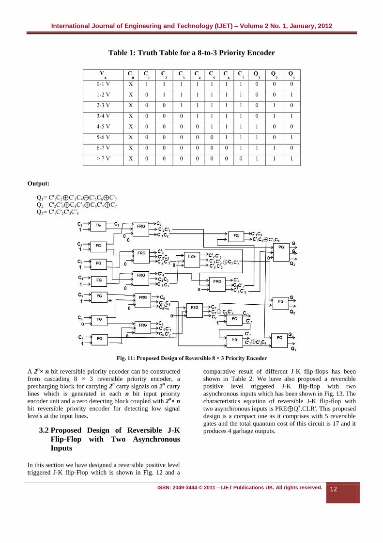
3.1 Proposed Design of Reversible Priority
Encoder
A 3-bit flash ADC is known as parallel A/D converter. It is
formed of a series of comparators, each one comparing the
input signal to a unique reference voltage. The comparator
outputs connect to the inputs of a priority encoder circuit,
which then produces a binary output. A stable reference
voltage Vref is provided by a precision voltage regulator as
part of the converter circuit. As the analog input voltage
exceeds the reference voltage at each comparator, the
comparator outputs will sequentially saturate to a high
state. The priority encoder generates a binary number
based on the highest-order active input; ignoring all other
active inputs. An n bit flash converter would require 2n-1
comparators, 2n resistors and the necessary logic. In this
section we have proposed the reversible design of 8-to-3
priority encoder which has been shown in Fig. 11. This
reversible design consists of 21 reversible gates having
quantum cost of 50 and 20 garbage outputs.
International Journal of Engineering and Technology (IJET) – Volume 2 No. 1, January, 2012
ISSN: 2049-3444 © 2011 – IJET Publications UK. All rights reserved. 12
Table 1: Truth Table for a 8-to-3 Priority Encoder
VA C
0 C
1 C
2 C
3 C
4 C
5 C
6 C
7 Q
3 Q
2 Q
1
0-1 V X 1 1 1 1 1 1 1 0 0 0
1-2 V X 0 1 1 1 1 1 1 0 0 1
2-3 V X 0 0 1 1 1 1 1 0 1 0
3-4 V X 0 0 0 1 1 1 1 0 1 1
4-5 V X 0 0 0 0 1 1 1 1 0 0
5-6 V X 0 0 0 0 0 1 1 1 0 1
6-7 V X 0 0 0 0 0 0 1 1 1 0
> 7 V X 0 0 0 0 0 0 0 1 1 1
Output:
Q1= C'1C2⊕C'3C4⊕C'5C6⊕C'7
Q2= C'2C'3⊕C3C'4⊕C6C'7⊕C7 Q3= C'1C'2C'3C'4
Fig. 11: Proposed Design of Reversible 8 × 3 Priority Encoder
A 2n× n bit reversible priority encoder can be constructed
from cascading 8 × 3 reversible priority encoder, a
precharging block for carrying 2n
carry signals on 2n carry
lines which is generated in each n bit input priority
encoder unit and a zero detecting block coupled with 2n× n
bit reversible priority encoder for detecting low signal
levels at the input lines.
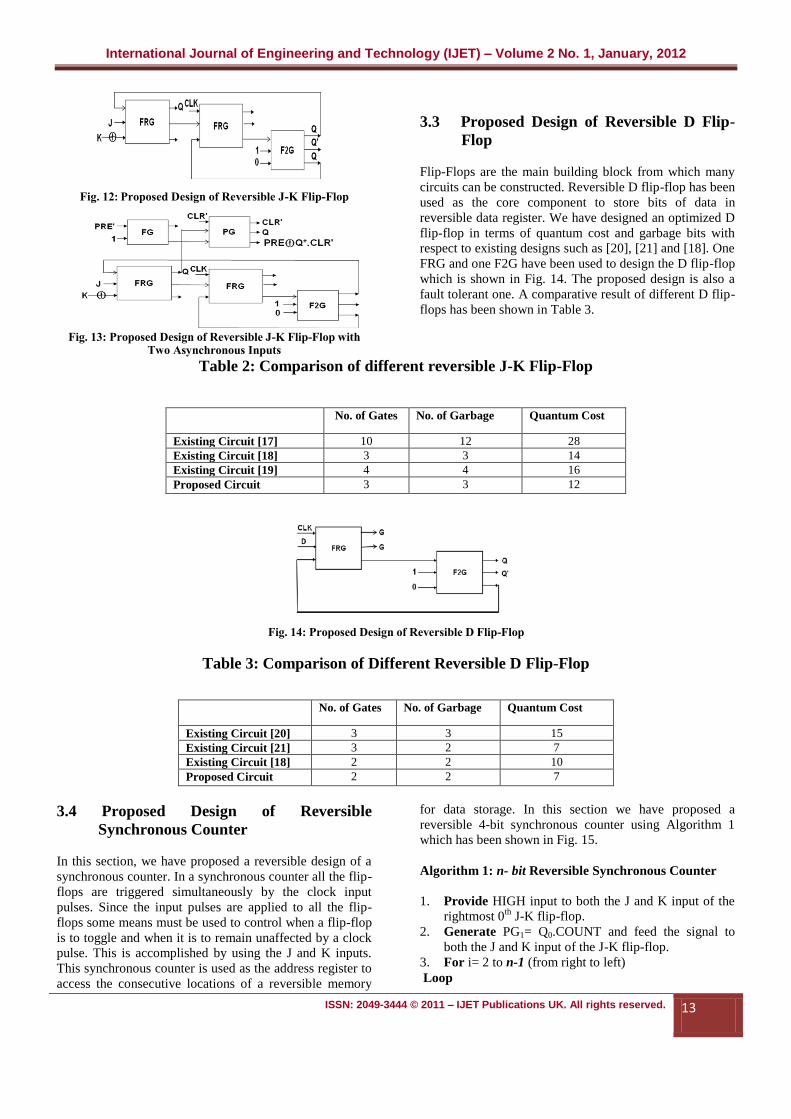
3.2 Proposed Design of Reversible J-K
Flip-Flop with Two Asynchronous
Inputs
In this section we have designed a reversible positive level
triggered J-K flip-Flop which is shown in Fig. 12 and a
comparative result of different J-K flip-flops has been
shown in Table 2. We have also proposed a reversible
positive level triggered J-K flip-flop with two
asynchronous inputs which has been shown in Fig. 13. The
characteristics equation of reversible J-K flip-flop with
two asynchronous inputs is PRE⊕Q+.CLR'. This proposed
design is a compact one as it comprises with 5 reversible
gates and the total quantum cost of this circuit is 17 and it
produces 4 garbage outputs.
International Journal of Engineering and Technology (IJET) – Volume 2 No. 1, January, 2012
ISSN: 2049-3444 © 2011 – IJET Publications UK. All rights reserved. 13
Fig. 12: Proposed Design of Reversible J-K Flip-Flop
Fig. 13: Proposed Design of Reversible J-K Flip-Flop with Two Asynchronous Inputs
3.3 Proposed Design of Reversible D Flip-
Flop
Flip-Flops are the main building block from which many
circuits can be constructed. Reversible D flip-flop has been
used as the core component to store bits of data in
reversible data register. We have designed an optimized D
flip-flop in terms of quantum cost and garbage bits with
respect to existing designs such as [20], [21] and [18]. One
FRG and one F2G have been used to design the D flip-flop
which is shown in Fig. 14. The proposed design is also a
fault tolerant one. A comparative result of different D flip-
flops has been shown in Table 3.
Table 2: Comparison of different reversible J-K Flip-Flop
Fig. 14: Proposed Design of Reversible D Flip-Flop
Table 3: Comparison of Different Reversible D Flip-Flop
No. of Gates No. of Garbage Quantum Cost
Existing Circuit [20] 3 3 15
Existing Circuit [21] 3 2 7
Existing Circuit [18] 2 2 10
Proposed Circuit 2 2 7
3.4 Proposed Design of Reversible
Synchronous Counter
In this section, we have proposed a reversible design of a
synchronous counter. In a synchronous counter all the flip-
flops are triggered simultaneously by the clock input
pulses. Since the input pulses are applied to all the flip-
flops some means must be used to control when a flip-flop
is to toggle and when it is to remain unaffected by a clock
pulse. This is accomplished by using the J and K inputs.
This synchronous counter is used as the address register to
access the consecutive locations of a reversible memory
for data storage. In this section we have proposed a
reversible 4-bit synchronous counter using Algorithm 1
which has been shown in Fig. 15.
Algorithm 1: n- bit Reversible Synchronous Counter
1. Provide HIGH input to both the J and K input of the
rightmost 0th
J-K flip-flop.
2. Generate PG1= Q0.COUNT and feed the signal to
both the J and K input of the J-K flip-flop.
3. For i= 2 to n-1 (from right to left)
Loop
No. of Gates No. of Garbage Quantum Cost
Existing Circuit [17] 10 12 28
Existing Circuit [18] 3 3 14
Existing Circuit [19] 4 4 16
Proposed Circuit 3 3 12
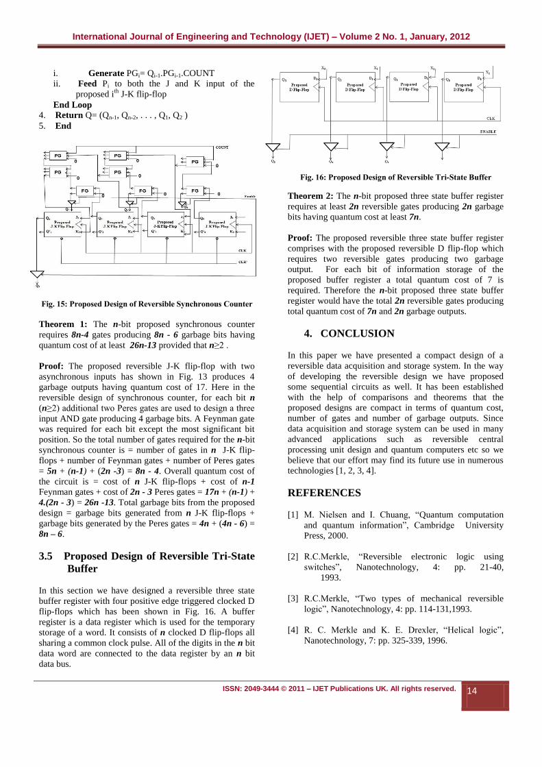
International Journal of Engineering and Technology (IJET) – Volume 2 No. 1, January, 2012
ISSN: 2049-3444 © 2011 – IJET Publications UK. All rights reserved. 14
i. Generate PGi= Qi-1.PGi-1.COUNT
ii. Feed Pi to both the J and K input of the
proposed ith
J-K flip-flop
End Loop 4. Return Q= (Qn-1, Qn-2, . . . , Q1, Q2 )
5. End
Fig. 15: Proposed Design of Reversible Synchronous Counter
Theorem 1: The n-bit proposed synchronous counter
requires 8n-4 gates producing 8n - 6 garbage bits having
quantum cost of at least 26n-13 provided that n≥2 .
Proof: The proposed reversible J-K flip-flop with two
asynchronous inputs has shown in Fig. 13 produces 4
garbage outputs having quantum cost of 17. Here in the
reversible design of synchronous counter, for each bit n
(n≥2) additional two Peres gates are used to design a three
input AND gate producing 4 garbage bits. A Feynman gate
was required for each bit except the most significant bit
position. So the total number of gates required for the n-bit
synchronous counter is = number of gates in n J-K flip-
flops + number of Feynman gates + number of Peres gates
= 5n + (n-1) + (2n -3) = 8n - 4. Overall quantum cost of
the circuit is = cost of n J-K flip-flops + cost of n-1
Feynman gates + cost of 2n - 3 Peres gates = 17n + (n-1) +
4.(2n - 3) = 26n -13. Total garbage bits from the proposed
design = garbage bits generated from n J-K flip-flops +
garbage bits generated by the Peres gates = 4n + (4n - 6) =
8n – 6.
3.5 Proposed Design of Reversible Tri-State
Buffer
In this section we have designed a reversible three state
buffer register with four positive edge triggered clocked D
flip-flops which has been shown in Fig. 16. A buffer
register is a data register which is used for the temporary
storage of a word. It consists of n clocked D flip-flops all
sharing a common clock pulse. All of the digits in the n bit
data word are connected to the data register by an n bit
data bus.
Fig. 16: Proposed Design of Reversible Tri-State Buffer
Theorem 2: The n-bit proposed three state buffer register
requires at least 2n reversible gates producing 2n garbage
bits having quantum cost at least 7n.
Proof: The proposed reversible three state buffer register
comprises with the proposed reversible D flip-flop which
requires two reversible gates producing two garbage
output. For each bit of information storage of the
proposed buffer register a total quantum cost of 7 is
required. Therefore the n-bit proposed three state buffer
register would have the total 2n reversible gates producing
total quantum cost of 7n and 2n garbage outputs.
4. CONCLUSION
In this paper we have presented a compact design of a
reversible data acquisition and storage system. In the way
of developing the reversible design we have proposed
some sequential circuits as well. It has been established
with the help of comparisons and theorems that the
proposed designs are compact in terms of quantum cost,
number of gates and number of garbage outputs. Since
data acquisition and storage system can be used in many
advanced applications such as reversible central
processing unit design and quantum computers etc so we
believe that our effort may find its future use in numerous
technologies [1, 2, 3, 4].
REFERENCES
[1] M. Nielsen and I. Chuang, “Quantum computation
and quantum information”, Cambridge University
Press, 2000.
[2] R.C.Merkle, “Reversible electronic logic using
switches”, Nanotechnology, 4: pp. 21-40,
1993.
[3] R.C.Merkle, “Two types of mechanical reversible
logic”, Nanotechnology, 4: pp. 114-131,1993.
[4] R. C. Merkle and K. E. Drexler, “Helical logic”,
Nanotechnology, 7: pp. 325-339, 1996.
International Journal of Engineering and Technology (IJET) – Volume 2 No. 1, January, 2012
ISSN: 2049-3444 © 2011 – IJET Publications UK. All rights reserved. 15
[5] R. Landauer, “Irreversibility and heat generation in
the computational process”, IBM Journal of Research
and Development, 5, pp. 183-191, 1961.
[6] Perkowski, M., A.Al-Rabadi, P. Kerntopf, A. Buller,
M. Chrzanowska-Jeske, A. Mishchenko, M. Azad
Khan, A. Coppola, S. Yanushkevich, V. Shmerko and
L. Jozwiak, 2001,“A general decomposition for
reversible logic”, Proc. RM’2001, Starkville, pp: 119-
138.
[7] Perkowski, M. and P. Kerntopf, 2001, “Reversible
Logic”, Invited tutorial, Proc. EURO-MICRO, Sept
2001, Warsaw, Poland.
[8] Thapliyal Himanshu, and M.B. Srinivas, 2005, “Novel
reversible TSG gate and its application for
designing reversible carry look ahead adder and other
adder architectures”, Proceedings of the 10th Asia-
Pacific Computer Systems Architecture Conference
(ACSAC 05). Lecture Notes of Computer Science,
Springer-Verlag, 3740: 775-786.
[9] Bennet, CH., 1973, “Logical reversibility of
computation”, IBM J. Res. Dev.,17: 525-532.
[10] H.M.H. Babu, M.R.Islam, A.R.Chowdhury, S.M.A.
Chowdhury, “Synthesis of full-adder circuit using
reversible logic”,in: 17th International Conference on
VLSI Design, 2004,pp.757-760.
[11] Biswas, A. K., Hasan, M. M., Chowdhury, A. R., and
Babu, M. H. H. 2008, “Efficient approaches for
designing reversible binary coded decimal adders”,
Microelectron. J. 39, 12, 1693- 1703.
[12] Parhami, B. 2006, “Fault tolerant reversible circuits”,
In Proc. of 40th Asimolar Conf. Signals, Systems, and
Computers, 1726-1729.
[13] Perkowski, M. 2003, “A hierarchical approach to
computer-aided design of quantum circuits”, 6th
International Symposium on Representations and
Methodology of Future Computing Technology, 201-
209.
[14] T.Toffoli,“ReversibleComputing”,TechmemoMIT/LC
S/TM151, MITLab for Computer Science,1980.
[15] E.Fredkin,E.Toffoli,“ConservativeLogic”,IntJ.Theor.
Ohys.21(1983)219-253.
[16] W. N. Hung, X. Song, G.Yang, J.Yang, and M.
Perkowski, “Optimal synthesis of multiple output
boolean functions using a set of quantum gates by
symbolic reachability analysis”, IEEE Trans.
Computer-Aided Design, 25(9):1652–1663,
Sept.2006.
[17] H. Thapliyal, M. B. Srinivas, and M. Zwolinski,” A
beginning in the reversible logic synthesis of
sequential circuits”,In Proc. the Military and
Aerospace Programmable Logic Devices Intl.
Conf., Washington, Sept. 2005.
[18] Abu Sadat Md. Sayem, Masashi Ueda, “Optimization
of reversible sequential circuits”, Journal of
Computing, Volume 2, Issue 6, June 2010, ISSN
2151-9617.
[19] Siva Kumar Sastry Hari, Shyam Shroff, Sk. Noor
Mahammad, V. Kamakoti, “Efficient building blocks
for reversible sequential circuit design”, Circuits and
Systems, 2006, MWSCAS '06, 49th IEEE
International Midwest Symposium on August 2006,
ISSN: 1548-3746.
[20] N. Huda, S. Anwar, L. Jamal, H.M.H. Babu, “Design
of Reversible Random Access Memory”, Dhaka
University Journal of Applied Science & Engineering:
Vol. 2(1) 31-38, July 2011.
[21] A. K. Biswas, “Efficient approaches for designing n-
bit processor” , unpublished.


![Journal of Engineering and Technology …iet-journals.org/archive/2012/feb_vol_2_no_2/...2 emission per tone in comparison with OPC [1,2,4]. With increasing production volumes, geopolymer](https://img.pdfslide.net/doc/110x75/5b1d4fdf7f8b9a64508b4f01/journal-of-engineering-and-technology-iet-emission-per-tone-in-comparison-with.jpg)