Embed Size (px)
Citation preview
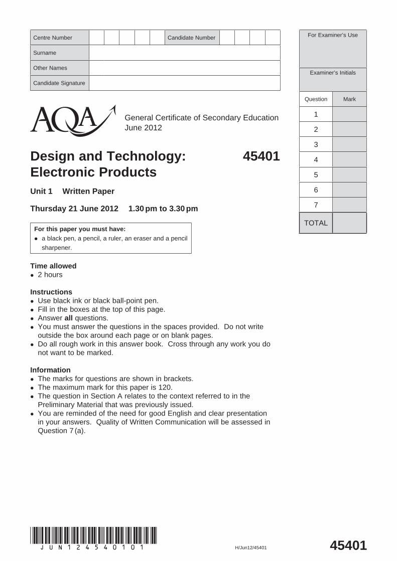
45401H/Jun12/45401(JUN124540101)
General Certificate of Secondary EducationJune 2012
Design and Technology: 45401Electronic ProductsUnit 1 Written Paper
Thursday 21 June 2012 1.30 pm to 3.30 pm
For this paper you must have: a black pen, a pencil, a ruler, an eraser and a pencil
sharpener.
Time allowed 2 hours
Instructions Use black ink or black ball-point pen. Fill in the boxes at the top of this page. Answer all questions. You must answer the questions in the spaces provided. Do not write
outside the box around each page or on blank pages. Do all rough work in this answer book. Cross through any work you do
not want to be marked.
Information The marks for questions are shown in brackets. The maximum mark for this paper is 120. The question in Section A relates to the context referred to in the
Preliminary Material that was previously issued. You are reminded of the need for good English and clear presentation
in your answers. Quality of Written Communication will be assessed in Question 7 (a).
Centre Number Candidate Number
Surname
Other Names
Candidate Signature
For Examiner’s Use
Examiner’s Initials
Question Mark
1
2
3
4
5
6
7
TOTAL

2 Do not write outside the
box
(02)H/Jun12/45401
You may need to use one or more of the following formulae when answering questions which include calculations.
Potential Difference Potential Difference = Current x Resistance (V = I x R)
Series Resistors Rtotal = R1 + R2 + R3 etc
Potential Divider
V out = R2
x Vs R1 + R2
where V out = signal value Vs = supply voltage R1 and R2 are resistance values
Vs
0V
R1
R2
V out
Time Constant Time Constant ≏ Resistance x Capacitance (T ≏ R x C)
Astable Frequency for 555 f = 1.44
(R1 + 2R2) x C
Mark Space Ratio = Time high
Time low
Time High = 0.693 x (R1 + R2) x C
Time Low = 0.693 x R2 x C
Inverting Op. Amps Gain = - Rf Where Rf = feedback resistor value
Rin Where Rin = input resistor value

3 Do not write outside the
box
(03)H/Jun12/45401
Turn over
You may need to use the following information when answering some of the questions.
The figures shown below and their decade multiples or submultiples are the series of preferred values in accordance with BS:2488.
E12 Resistor series 10, 12, 15, 18, 22, 27, 33, 39, 47, 56, 68, 82
E24 Resistor series 10, 11, 12, 13, 15, 16, 18, 20, 22, 24, 27, 30, 33, 36, 39, 43, 47, 51, 56, 62, 68, 75, 82, 91
Capacitor series 10, 22, 47
Resistor Colour Code
Colour Band 1 Band 2 Band 3(No. of 0s)
Band 4(Tolerance)
Black 0 0 None
Brown 1 1 0
Red 2 2 00
Orange 3 3 000
Yellow 4 4 0000
Green 5 5 00000
Blue 6 6 000000
Violet 7 7 –
Grey 8 8 –
White 9 9 –
Gold = 5%
Silver = 10%
Turn over for the first question
4 Do not write outside the
box
(04)H/Jun12/45401
Section A
Answer all questions in the spaces provided.
You are advised to spend about 35 minutes on this question.
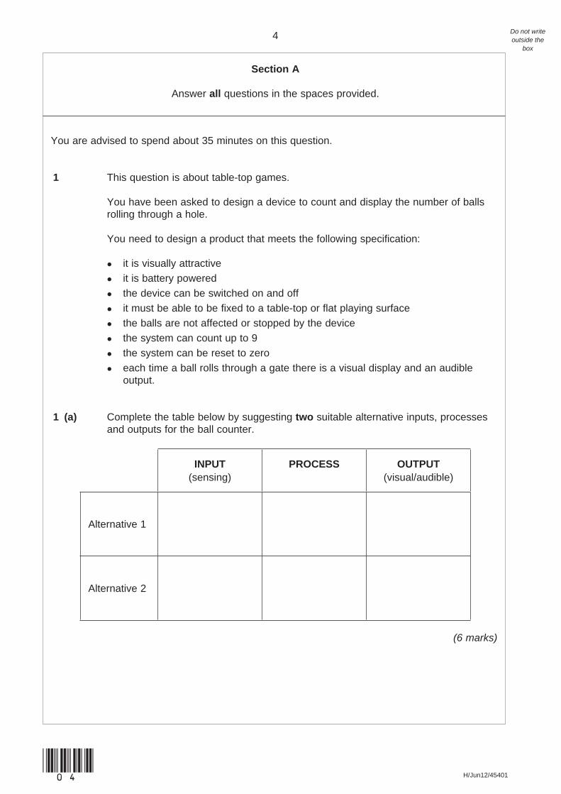
1 This question is about table-top games.
You have been asked to design a device to count and display the number of balls rolling through a hole.
You need to design a product that meets the following specification:
it is visually attractive it is battery powered the device can be switched on and off it must be able to be fixed to a table-top or flat playing surface the balls are not affected or stopped by the device the system can count up to 9 the system can be reset to zero each time a ball rolls through a gate there is a visual display and an audible
output.
1 (a) Complete the table below by suggesting two suitable alternative inputs, processes and outputs for the ball counter.
INPUT(sensing)
PROCESS OUTPUT(visual/audible)
Alternative 1
Alternative 2
(6 marks)

5 Do not write outside the
box
(05)H/Jun12/45401
Turn over
1 (b) Using notes and sketches, produce an initial idea for the design of the product casing only.
Your design must meet the following specification points:
it is visually attractive it is battery powered the device can be switched on and off it must be able to be fixed to a table-top or flat playing surface the balls are not affected or stopped by the device.
(6 marks)Question 1 continues on the next page
6 Do not write outside the
box
(06)H/Jun12/45401
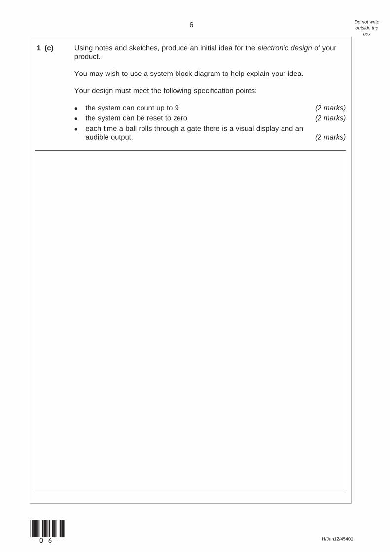
1 (c) Using notes and sketches, produce an initial idea for the electronic design of your product.
You may wish to use a system block diagram to help explain your idea.
Your design must meet the following specification points:
the system can count up to 9 (2 marks) the system can be reset to zero (2 marks) each time a ball rolls through a gate there is a visual display and an
audible output. (2 marks)

7 Do not write outside the
box
(07)H/Jun12/45401
Turn over
1 (d) In the box below use notes and sketches to produce a fully detailed design of your product that shows clearly how the specification points on page 4 have been met.
Marks will be awarded for:
constructional details showing how the product is made (6 marks) operational details showing how the circuit works (6 marks) communication of the design (quality of graphic presentation). (3 marks)
____33
8 Do not write outside the
box
(08)H/Jun12/45401
Section B
Answer all questions in the spaces provided.
You are advised to spend about 10 minutes on this question.
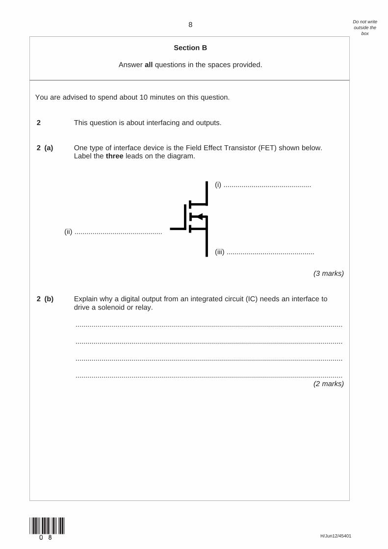
2 This question is about interfacing and outputs.
2 (a) One type of interface device is the Field Effect Transistor (FET) shown below. Label the three leads on the diagram.
(iii) ............................................
(ii) ............................................
(i) ............................................
(3 marks)
2 (b) Explain why a digital output from an integrated circuit (IC) needs an interface to drive a solenoid or relay.
......................................................................................................................................
......................................................................................................................................
......................................................................................................................................
......................................................................................................................................(2 marks)
9 Do not write outside the
box
(09)H/Jun12/45401
Turn over
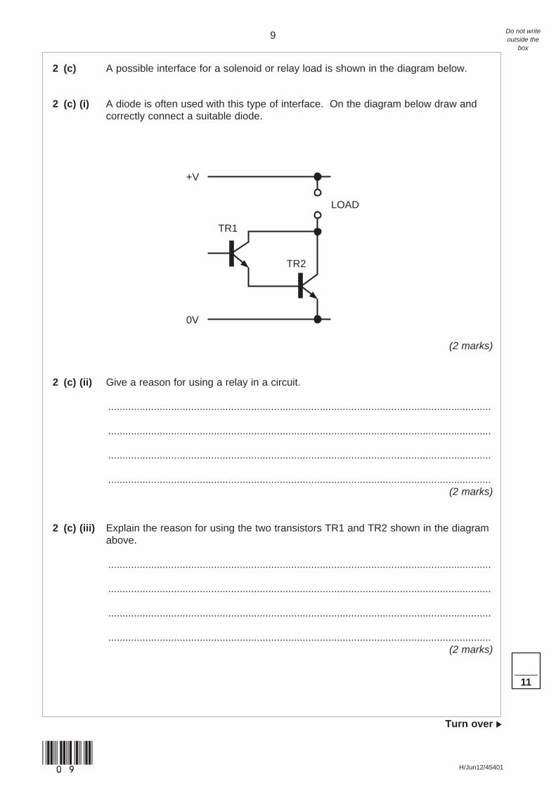
2 (c) A possible interface for a solenoid or relay load is shown in the diagram below.
2 (c) (i) A diode is often used with this type of interface. On the diagram below draw and correctly connect a suitable diode.
TR2
TR1
+V
LOAD
0V
(2 marks)
2 (c) (ii) Give a reason for using a relay in a circuit.
......................................................................................................................................
......................................................................................................................................
......................................................................................................................................
......................................................................................................................................(2 marks)
2 (c) (iii) Explain the reason for using the two transistors TR1 and TR2 shown in the diagram above.
......................................................................................................................................
......................................................................................................................................
......................................................................................................................................
......................................................................................................................................(2 marks)
____11

10 Do not write outside the
box
H/Jun12/45401(10)
You are advised to spend about 15 minutes on this question.
3 This question is about Printed Circuit Board (PCB) design and manufacture.
Prototype circuits might be produced by breadboarding or using a Computer-Aided Design (CAD) package.
3 (a) (i) Explain why a breadboard is used when designing circuits.
......................................................................................................................................
......................................................................................................................................
......................................................................................................................................
......................................................................................................................................(2 marks)
3 (a) (ii) Explain why CAD is used as an alternative to breadboarding.
......................................................................................................................................
......................................................................................................................................
......................................................................................................................................
......................................................................................................................................(2 marks)
3 (b) Explain why surface mounting is replacing through-hole mounting of components.
......................................................................................................................................
......................................................................................................................................
......................................................................................................................................
......................................................................................................................................(2 marks)
3 (c) Describe how surface mount components might be placed and attached to a PCB.
Placed ..........................................................................................................................
......................................................................................................................................
Attached .......................................................................................................................
......................................................................................................................................(2 marks)

11 Do not write outside the
box
H/Jun12/45401
Turn over
(11)
3 (d) Give two reasons why the use of surface mounted components might be difficult when prototyping.
Reason 1 ......................................................................................................................
......................................................................................................................................
Reason 2 ......................................................................................................................
......................................................................................................................................(2 marks)
3 (e) Complete the table below to show six stages in the design and production of either a photo etched or a machined PCB.
State method ................................................................................................................
Stage Description
1
2
3
4
5
6
(6 marks)____
16
12 Do not write outside the
box
H/Jun12/45401(12)
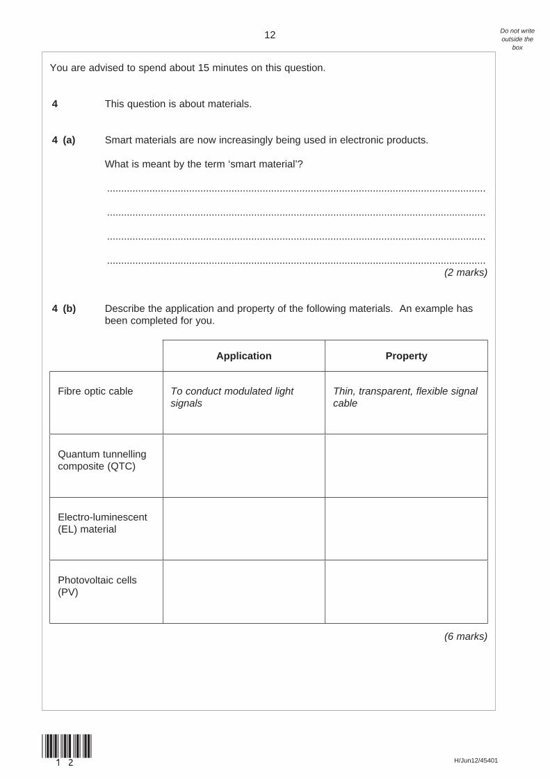
You are advised to spend about 15 minutes on this question.
4 This question is about materials.
4 (a) Smart materials are now increasingly being used in electronic products.
What is meant by the term ‘smart material’?
......................................................................................................................................
......................................................................................................................................
......................................................................................................................................
......................................................................................................................................(2 marks)
4 (b) Describe the application and property of the following materials. An example has been completed for you.
Application Property
Fibre optic cable To conduct modulated light signals
Thin, transparent, flexible signal cable
Quantum tunnelling composite (QTC)
Electro-luminescent (EL) material
Photovoltaic cells(PV)
(6 marks)

13 Do not write outside the
box
H/Jun12/45401
Turn over
(13)
4 (c) New developments make many products obsolete quickly.
Mobile phones are a good example.
4 (c) (i) What is meant by planned obsolescence?
......................................................................................................................................
......................................................................................................................................
......................................................................................................................................
......................................................................................................................................(2 marks)
4 (c) (ii) Describe what can be done by a user of an electronic product to reduce the impact of obsolescence.
......................................................................................................................................
......................................................................................................................................
......................................................................................................................................
......................................................................................................................................(2 marks)
____12
Turn over for the next question
14 Do not write outside the
box
H/Jun12/45401(14)
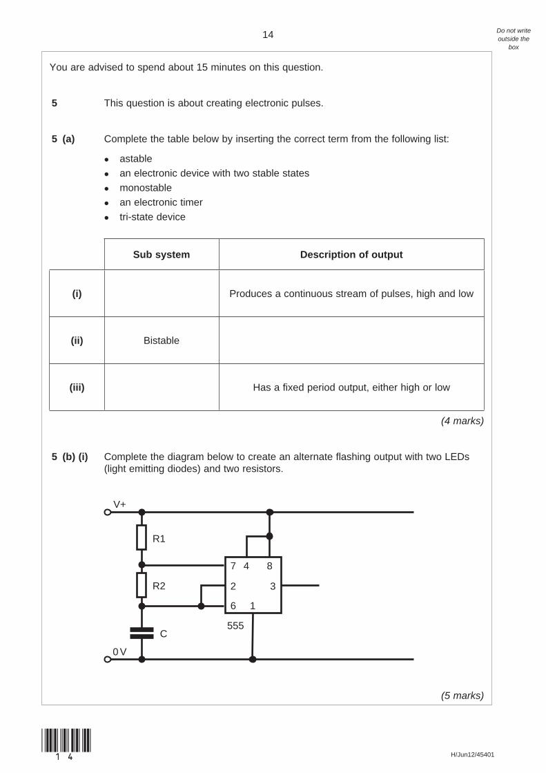
You are advised to spend about 15 minutes on this question.
5 This question is about creating electronic pulses.
5 (a) Complete the table below by inserting the correct term from the following list:
astable an electronic device with two stable states monostable an electronic timer tri-state device
Sub system Description of output
(i) Produces a continuous stream of pulses, high and low
(ii) Bistable
(iii) Has a fixed period output, either high or low
(4 marks)
5 (b) (i) Complete the diagram below to create an alternate flashing output with two LEDs (light emitting diodes) and two resistors.
0 V
R1
R2
C
V+
555
1
2 3
6
7 4 8
(5 marks)

15 Do not write outside the
box
H/Jun12/45401
Turn over
(15)
5 (b) (ii) In the graph space below, draw a typical output signal at pin 3 shown on the circuit diagram in Question 5 (b) (i).
Label the mark, the space and the period or cycle.
Time (seconds)
Voltage
(4 marks)
5 (b) (iii) Using the correct formula from the information on page 2, calculate the value of the Time Low for the pulse stream if the capacitor value used is 10 uF and the resistor value 100 K.
State formula used .......................................................................................................
......................................................................................................................................(1 mark)
Show calculation and units used .................................................................................
......................................................................................................................................
......................................................................................................................................
......................................................................................................................................(2 marks)
Calculated Time Low ...................................................................................................(1 mark)
____17

16
H/Jun12/45401
Blank page
DO NOT WRITE ON THIS PAGEANSWER IN THE SPACES PROVIDED
(16)
17 Do not write outside the
box
H/Jun12/45401
Turn over
(17)
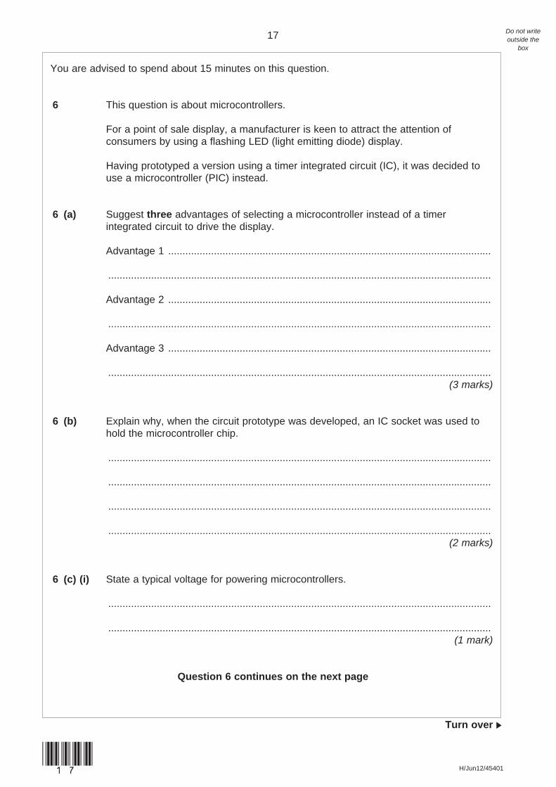
You are advised to spend about 15 minutes on this question.
6 This question is about microcontrollers.
For a point of sale display, a manufacturer is keen to attract the attention of consumers by using a flashing LED (light emitting diode) display.
Having prototyped a version using a timer integrated circuit (IC), it was decided to use a microcontroller (PIC) instead.
6 (a) Suggest three advantages of selecting a microcontroller instead of a timer integrated circuit to drive the display.
Advantage 1 .................................................................................................................
......................................................................................................................................
Advantage 2 .................................................................................................................
......................................................................................................................................
Advantage 3 .................................................................................................................
......................................................................................................................................(3 marks)
6 (b) Explain why, when the circuit prototype was developed, an IC socket was used to hold the microcontroller chip.
......................................................................................................................................
......................................................................................................................................
......................................................................................................................................
......................................................................................................................................(2 marks)
6 (c) (i) State a typical voltage for powering microcontrollers.
......................................................................................................................................
......................................................................................................................................(1 mark)
Question 6 continues on the next page
18 Do not write outside the
box
H/Jun12/45401(18)
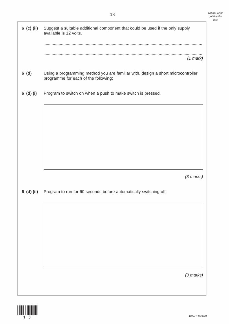
6 (c) (ii) Suggest a suitable additional component that could be used if the only supply available is 12 volts.
......................................................................................................................................
......................................................................................................................................(1 mark)
6 (d) Using a programming method you are familiar with, design a short microcontroller programme for each of the following:
6 (d) (i) Program to switch on when a push to make switch is pressed.
(3 marks)
6 (d) (ii) Program to run for 60 seconds before automatically switching off.
(3 marks)

19 Do not write outside the
box
H/Jun12/45401
Turn over
(19)
6 (d) (iii) Program to drive two sets of LEDs on and then off at 1 second intervals.
(4 marks)
____17
Turn over for the next question
20 Do not write outside the
box
H/Jun12/45401(20)
You are advised to spend about 15 minutes on this question.
7 This question is about testing circuits.
You will be marked on your quality of written communication in this question.
7 (a) Describe methods you would use to test a printed circuit board (PCB).
......................................................................................................................................
......................................................................................................................................
......................................................................................................................................
......................................................................................................................................
......................................................................................................................................
......................................................................................................................................
......................................................................................................................................
......................................................................................................................................
......................................................................................................................................
......................................................................................................................................
......................................................................................................................................
......................................................................................................................................
......................................................................................................................................
......................................................................................................................................
......................................................................................................................................
......................................................................................................................................
......................................................................................................................................
......................................................................................................................................
......................................................................................................................................
......................................................................................................................................(8 marks)
21 Do not write outside the
box
H/Jun12/45401(21)
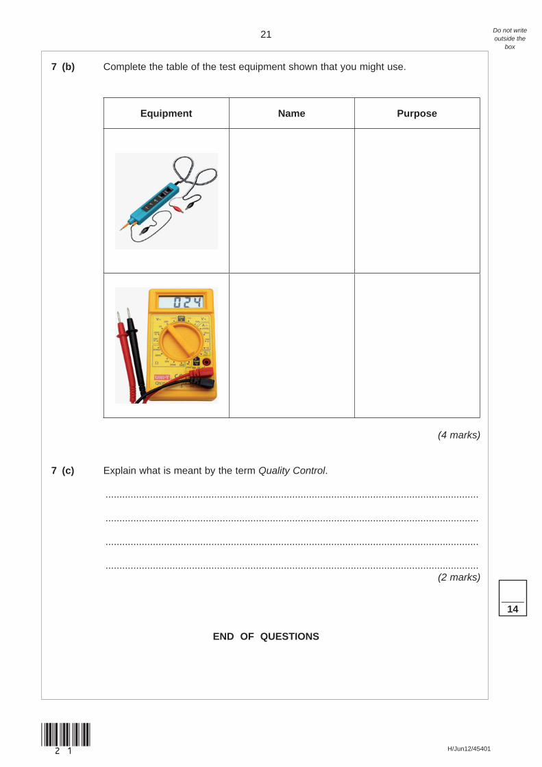
7 (b) Complete the table of the test equipment shown that you might use.
Equipment Name Purpose
(4 marks)
7 (c) Explain what is meant by the term Quality Control.
......................................................................................................................................
......................................................................................................................................
......................................................................................................................................
......................................................................................................................................(2 marks)
____14
END OF QUESTIONS

22
H/Jun12/45401
There are no questions printed on this page
DO NOT WRITE ON THIS PAGEANSWER IN THE SPACES PROVIDED
(22)
23
H/Jun12/45401
There are no questions printed on this page
DO NOT WRITE ON THIS PAGEANSWER IN THE SPACES PROVIDED
(23)

24
H/Jun12/45401
There are no questions printed on this page
DO NOT WRITE ON THIS PAGEANSWER IN THE SPACES PROVIDED
(24)
ACKNOWLEDGEMENT OF COPYRIGHT-HOLDERS AND PUBLISHERS
Permission to reproduce all copyright material has been applied for. In some cases, efforts to contact copyright-holders have been unsuccessful and AQA will be happy to rectify any omissions of acknowledgements in future papers if notified.
Copyright © 2012 AQA and its licensors. All rights reserved.